1. Introduction
The increasing demand for Electric Vehicles (EVs) is driven by their environmental benefits, higher energy efficiency, and quiet operation. One of the emerging functionalities of EVs is Vehicle-to-Grid (V2G) integration, which enables the bi-directional transfer of energy between the EV battery and the power grid. To support this function, a bi-directional charger is essential, consisting of an AC–DC converter and a DC–DC converter that allow power flow during both charging, grid-to-battery, and discharging, battery-to-grid, modes [
1,
2,
3,
4].
Among various DC–DC converter topologies, the Phase-Shifted Full-Bridge (PSFB) converter is widely used in high-power applications due to its ability to achieve Zero-Voltage Switching (ZVS), thereby improving conversion efficiency [
5,
6,
7]. However, PSFB converters suffer from certain drawbacks, especially under light-load conditions, such as high Electromagnetic Interference (EMI), increased voltage stress across rectifier diodes, and diminished efficiency caused by duty cycle loss and high circulating currents [
8,
9,
10].
To address these limitations, soft-switching resonant converters have become an attractive alternative. In particular, the LLC resonant full-bridge converter offers benefits such as full-range ZVS operation for primary switches, reduced EMI, and improved efficiency at high frequencies [
11,
12,
13]. Nonetheless, the LLC converter experiences performance degradation in discharge mode, where the magnetizing inductance forms a parallel path across the full bridge. This effectively transitions the converter into a series resonant configuration, resulting in a significant drop in efficiency when operating off-resonance and making capacitive mode operation likely [
12,
13,
14].
Several variants of the bi-directional CLLLC resonant converter have been proposed to extend soft-switching over both charging and discharging operations by incorporating additional LC circuits on the secondary side [
15,
16,
17,
18,
19,
20,
21,
22,
23]. While this improves ZVS capability, especially in discharge mode, it poses challenges in wide-output-voltage applications such as EV battery charging. Achieving a broad output range in Constant Current (CC) mode often requires a smaller magnetizing inductance, which increases the turn-off current and switching losses. Moreover, the wide variation in switching frequency required to accommodate load fluctuations leads to an increased circulating current and reduced efficiency [
14,
15].
To overcome these challenges, this work presents a novel bi-directional CLLLC resonant converter topology for V2G systems. The converter introduces an auxiliary LC resonant network connected via a third transformer winding, which functions as a frequency-dependent variable inductor. This auxiliary branch effectively enhances the total magnetizing inductance seen by the primary side, enabling soft-switching over a wide operating range.
At the main resonant frequency , the converter operates in Constant Voltage (CV) mode, where the effective magnetizing inductance reaches its maximum value. This reduces conduction and turn-off switching losses for the primary switches. A secondary resonant frequency is also supported, where the effective magnetizing inductance , formed by the parallel combination of the main and auxiliary branches, resonates with the primary and secondary inductors and capacitors. At this frequency, the system operates in CC mode and achieves Zero-Voltage and Zero-Current Switching (ZVZCS) conditions, all without requiring dynamic frequency modulation.
In discharge mode, the increased effective magnetizing inductance ensures ZVS across the entire load range, minimizing switching and circulating current losses. Since the proposed topology retains the operational structure of the conventional CLLLC converter, it benefits from its inherent advantages while significantly improving its performance through soft-switching and fixed-frequency operation. These features make it highly suitable for V2G applications demanding high efficiency, power density, and controllability.
2. Steady-State Analysis
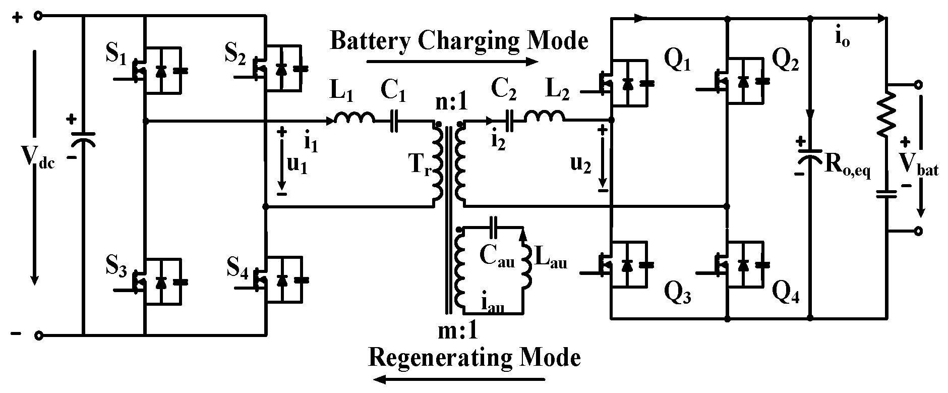
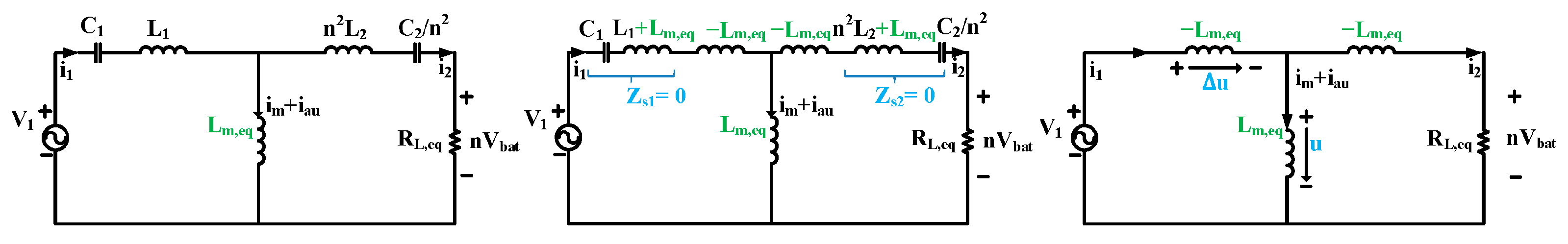
The circuit diagram of the proposed bi-directional resonant converter is illustrated in
Figure 1. Structurally, it resembles a conventional CLLLC topology, with the addition of an auxiliary LC branch connected via a tertiary winding on the transformer. This auxiliary branch introduces a frequency-dependent inductive path that plays a significant role in improving the converter’s soft-switching performance.
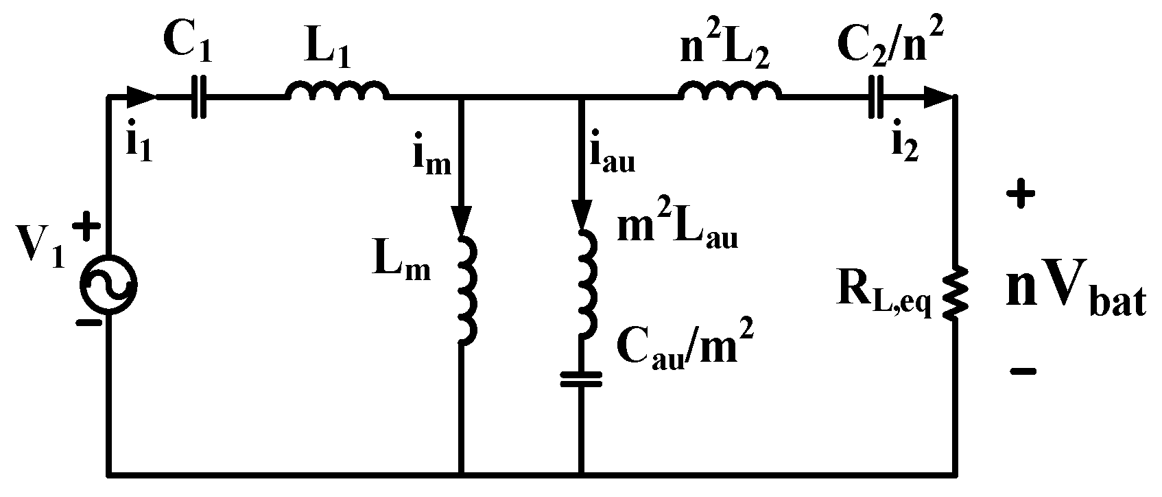
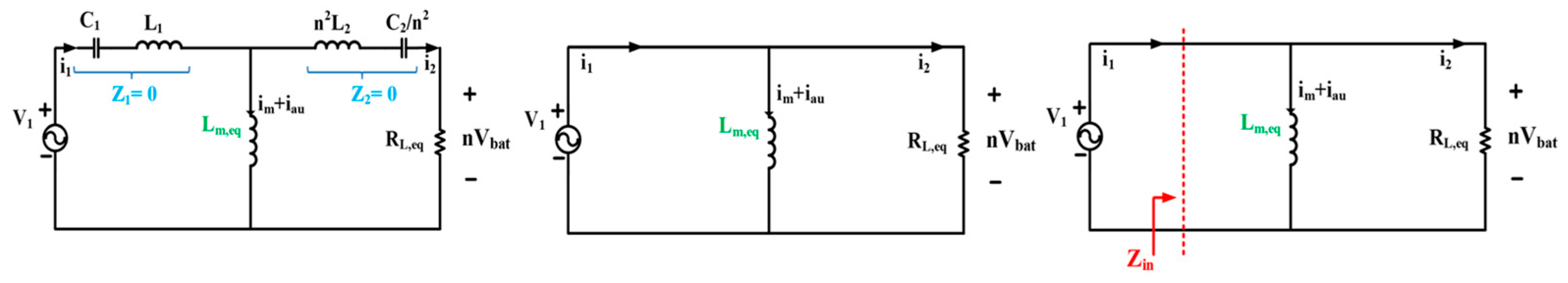
On the primary side, the four switches form a full-bridge inverter that converts the DC input into a high-frequency AC waveform. This waveform is passed through the transformer to the secondary side, where the rectifier switches reconstruct the output DC voltage. The equivalent AC circuit of the converter is shown in
Figure 2.
The transformer provides galvanic isolation with a turns ratio of n:1. The resonant tank consists of primary- and secondary-side leakage inductances and , magnetizing inductance , resonant capacitors and , and the auxiliary components and . Capacitors and also support flux balancing and resonate with and , respectively. The auxiliary LC circuit is linked through a third transformer winding with a turn ratio m:1, acting as a tunable branch that modifies the effective magnetizing impedance depending on the switching frequency.
2.1. Effective Magnetizing Inductance Design
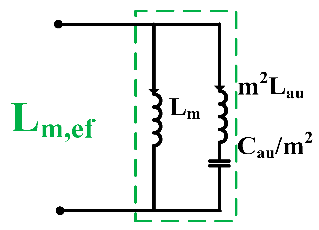
The AC equivalent model of the converter is shown in
Figure 2, from which the effective impedance values can be derived as shown in
Figure 3. The effective magnetizing inductance is expressed in Equation (1):
where
is the switching frequency,
, and
.
In the following analysis,
s =
jω represents the complex frequency variable in the Laplace domain, where
ω = 2
πf is the angular frequency. The values of the inductances can be calculated as follows:
where
, effective magnetizing impedance
, and
are the magnetizing impedance, effective magnetizing impedance, and input impedance, respectively.
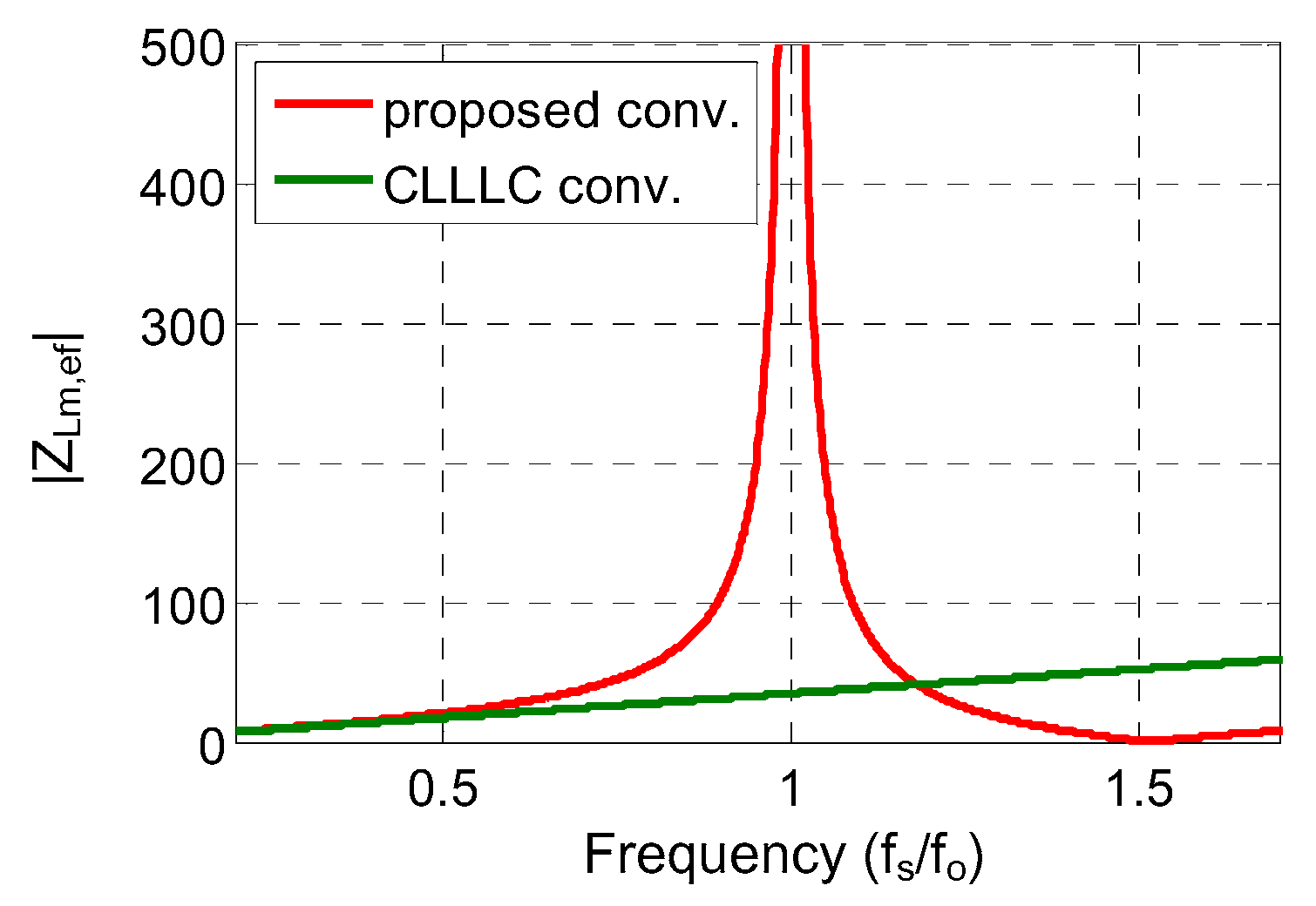
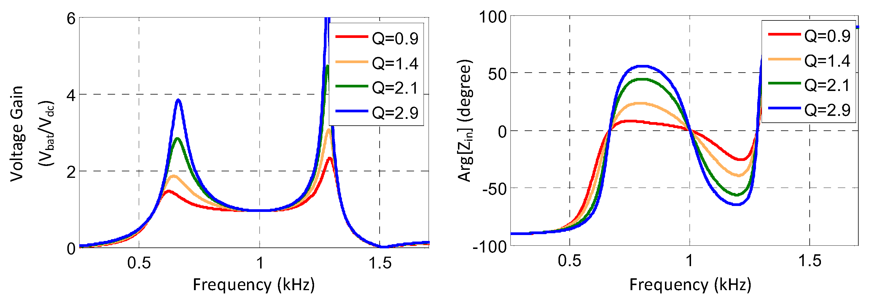
Figure 4 compares the magnetizing impedance of the proposed converter with that of the conventional CLLLC converter. The use of the auxiliary LC circuit clearly boosts the magnetizing impedance, particularly around the designed resonant frequency. When the auxiliary circuit is tuned such that
and
resonate with
at
, the effective impedance approaches an extremely high value, and is theoretically infinite.
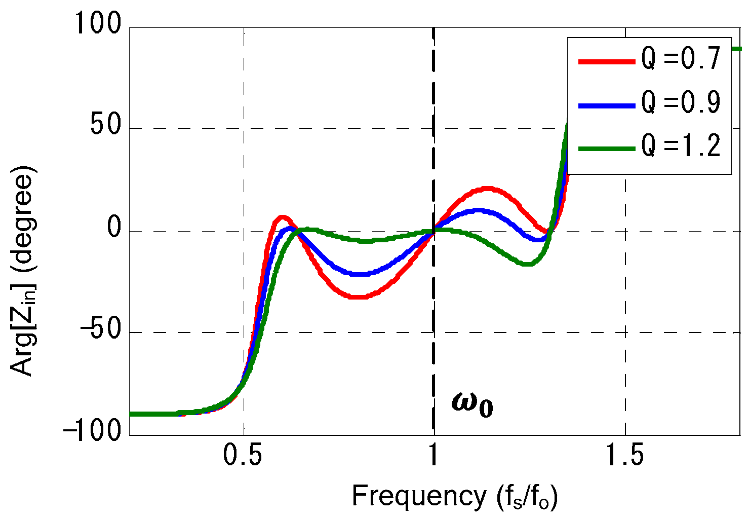
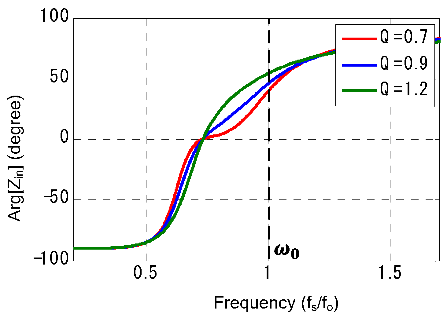
To further understand the advantage of this increased effective inductance,
Figure 5 and
Figure 6 illustrate the phase of the input impedance as a function of frequency. In the proposed converter, the input impedance phase approaches zero at the resonant frequency
, indicating that the input voltage and current are in a phase: this is known as the Zero Phase Angle (ZPA) operation.
By contrast, the input impedance of the conventional CLLLC converter remains inductive over the same frequency range. The inductive nature results in higher switching losses, particularly under varying load conditions.
2.2. Voltage Gain Characteristic
Using the First Harmonic Approximation (FHA), the voltage gain
M of the proposed converter during battery charging is derived as follows:
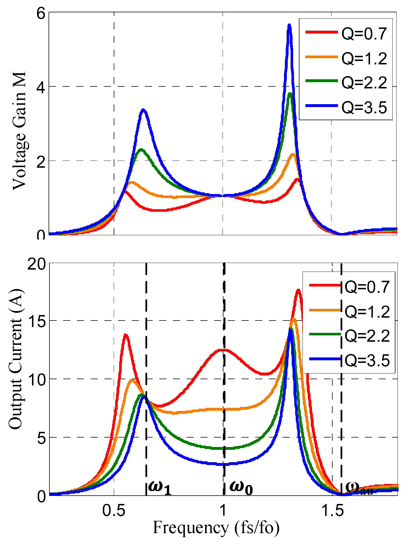
Figure 7 illustrates the relationship between voltage gain and output current as a function of switching frequency. It is observed that at the main resonant frequency
, the voltage gain becomes unity, independent of the load conditions. This makes the resonant frequency a suitable operating point for implementing CV mode charging, where a fixed output voltage is desired.
At this frequency, although the gain remains constant, the current output becomes largely load-dependent. Interestingly, the output current exhibits minimal variation in response to load changes, suggesting that CC mode can also be reliably achieved at this frequency.
Between the two resonant frequencies denoted as and , the gain varies according to load and frequency, making this region suitable for the discharge mode operation. The converter thus flexibly supports both CV and CC modes at fixed frequencies and uses the intermediate range for energy-return applications.
2.3. CC Charge Mode Implementation
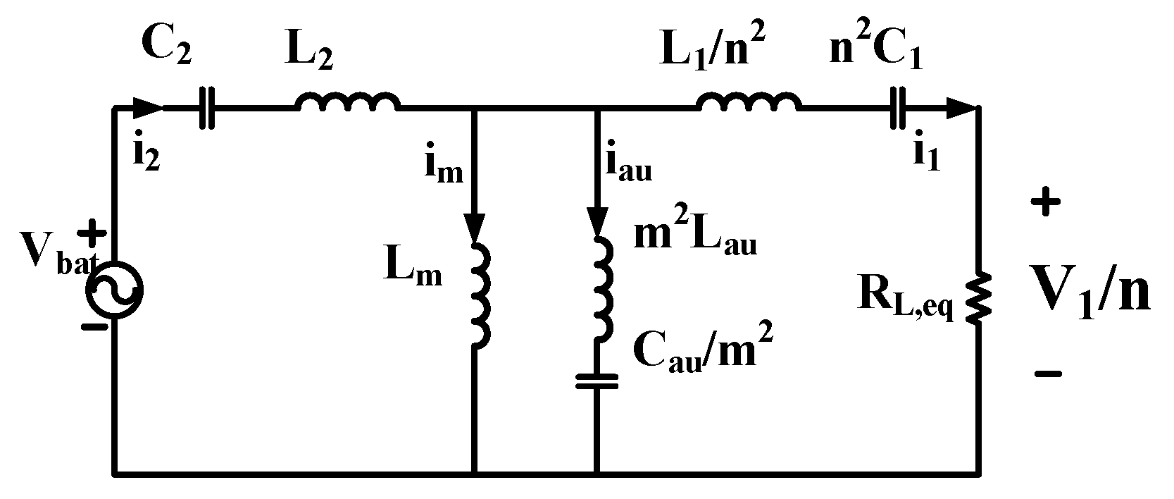
The simplified circuit model of the converter under CC mode operation is presented in
Figure 8. Using Kirchhoff’s laws, the system dynamics at the resonant frequency can be described with the following set of equations:
The simplified equivalent circuit in CC mode as shown in
Figure 8 is analyzed based on Kirchhoff’s theory. Kirchhoff’s equations for the circuit are then derived as
From Equation (11), it can be concluded that the output current remains nearly constant regardless of load variations. The current magnitude depends primarily on the input voltage and the effective magnetizing impedance . Since the resonant capacitors and are tuned to resonate with inductors and at frequency for the overall resonant impedance , becomes negligible, leaving primarily governed by Vin and .
Figure 7 demonstrates that across a range of load resistances
, the average output current remains nearly flat at
, validating its suitability for CC operation.
Additionally, under this condition, the input impedance
is a real number, which satisfies the ZPA condition, as described in the following:
2.4. CV Charge Mode Implementation
The simplified equivalent circuit for the converter operating in CV charge mode is shown in
Figure 9. In this mode, the converter is also operated at the resonant frequency
, and the circuit behavior is analyzed using Kirchhoff’s law.
The system equations governing circuit dynamics are
From Equation (14) and the circuit shown in
Figure 9, it becomes evident that the output voltage
remains relatively constant, irrespective of the load variation. This condition is satisfied when the resonant frequency
causes the impedance of the auxiliary LC branch to become very high, effectively isolating it. In this case, the output voltage aligns with the reflected input voltage across the secondary, making the CV mode operation feasible.
The input impedance of the system under CV mode can be expressed as follows:
Since
is dependent on the load resistance
, the phase angle of the input impedance can be evaluated as follows:
If the effective magnetizing impedance is sufficiently large, the phase angle of becomes close to zero, satisfying the ZPA condition. This ensures that the voltage and current waveforms remain in phase at the primary side, improving the power transfer and minimizing reactive losses.
To guarantee this condition, the auxiliary capacitor should be selected to resonate with and at the resonant frequency. This maximizes the impedance of the auxiliary path and ensures minimal phase deviation in CV mode.
2.5. Discharge Mode Implementation
In discharge mode, the converter operates by transferring energy from the EV battery back to the DC link, enabling V2G functionality. The equivalent circuit during this mode is presented in
Figure 10, and its corresponding voltage gain and impedance characteristics are shown in
Figure 11.
The switching frequency in this mode operates between two key frequencies, and . As with conventional CLLLC topologies, achieving a wide voltage gain and low-frequency variation requires a small magnetizing inductance . In the proposed converter, the auxiliary LC branch allows the use of a low base magnetizing inductance while still maintaining a large effective magnetizing inductance, reducing turn-off losses.
As indicated in
Figure 11, the phase of the input impedance remains inductive throughout the discharge operation. This behavior ensures ZVS is achieved for the secondary-side switches across the entire operating range.
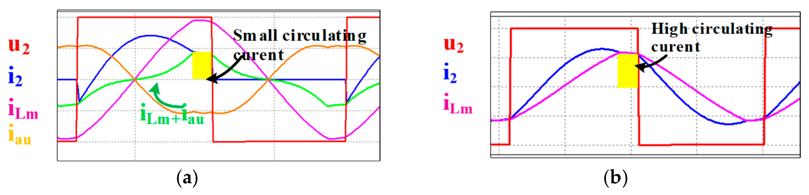
Figure 12 compares the current waveforms of the secondary switches for both the proposed and the conventional CLLLC converter.
In the conventional design, the circulating current equals the peak value of the magnetizing current. Since
must be small to allow gain flexibility, the magnetizing current is relatively high, resulting in large circulating losses (
Figure 12b).
In the proposed topology, the circulating current corresponds to the peak value of the total current i2, which is the sum of the magnetizing current
and the auxiliary current
. Notably,
and
flow in opposite directions, which leads to partial cancellation and reduces the total circulating current (
Figure 12a).
As a result, the proposed converter demonstrates significantly lower circulating losses during discharge mode while still enabling the wide voltage gain and soft-switching operation: benefits that are not easily achieved in conventional CLLLC converters without sacrificing efficiency.
2.6. Control Strategy and Mode Transition Framework
The proposed converter employs a comprehensive control strategy that manages seamless transitions between Constant Current (CC) and Constant Voltage (CV) charging modes through carefully designed threshold-based switching logic. The CC to CV transition is initiated when the battery voltage reaches 58.8 V with a tolerance of ±0.2 V, incorporating a 100 ms delay to prevent oscillation during the switching process. Conversely, the CV to CC transition occurs when the battery current drops to 0.5 A (±0.1 A) using hysteresis control to ensure stable operation. The system continuously monitors battery State-Of-Charge (SOC) with temperature compensation implemented at −2 mV/°C to optimize charging efficiency across varying environmental conditions. Safety protection is integrated through over-current protection limiting the current to 65 A maximum and over-voltage protection capping the voltage at 62 V maximum to prevent damage to both the converter and battery systems.
Real-world implementation considerations include an optimized transient response achieving load-step response settling times below 100 ms through feedforward compensation techniques that anticipate load changes. For Vehicle-To-Grid (V2G) operation, the system incorporates Phase-Locked Loop (PLL) synchronization maintaining ±1° phase accuracy to ensure proper grid integration. Communication with vehicle systems is facilitated through CAN bus integration supporting standard vehicle communication protocols, while fault management employs a three-tier protection system with automatic recovery capability to ensure reliable operation under various fault conditions.
The control system architecture centers on a TMS320F28379D DSP (Digikey, Seoul, South Korea) master controller operating at 150 MHz processing capability, providing sufficient computational power for real-time control operations. The control hierarchy implements a three-level structure with supervisory control operating at 10 Hz for overall system management, mode management functions at 100 Hz for transition control, and power regulation at 10 kHz for precise power control. Mode transition logic utilizes state machine implementation with anti-windup protection during transitions to prevent control system instability and ensure smooth operation during mode changes, maintaining system stability throughout the charging and discharging cycles.
3. Operation Principle
In the proposed bi-directional resonant converter, the mode of operation changes depending on whether the system is charging the battery (Powering Mode) or discharging it (Return Mode). The switches are controlled accordingly to enable a unidirectional power transfer in each mode.
During the charging mode, the primary-side switches (S1–S4) are actively controlled to drive the transformer, while the secondary-side switches (Q1–Q4) operate as synchronous rectifiers. Conversely, during discharging mode, the roles are reversed: the secondary switches are controlled, and the body diodes of the primary-side switches serve as passive rectifiers.
To simplify the analysis, the following assumptions are made:
3.1. Battery Charging Mode
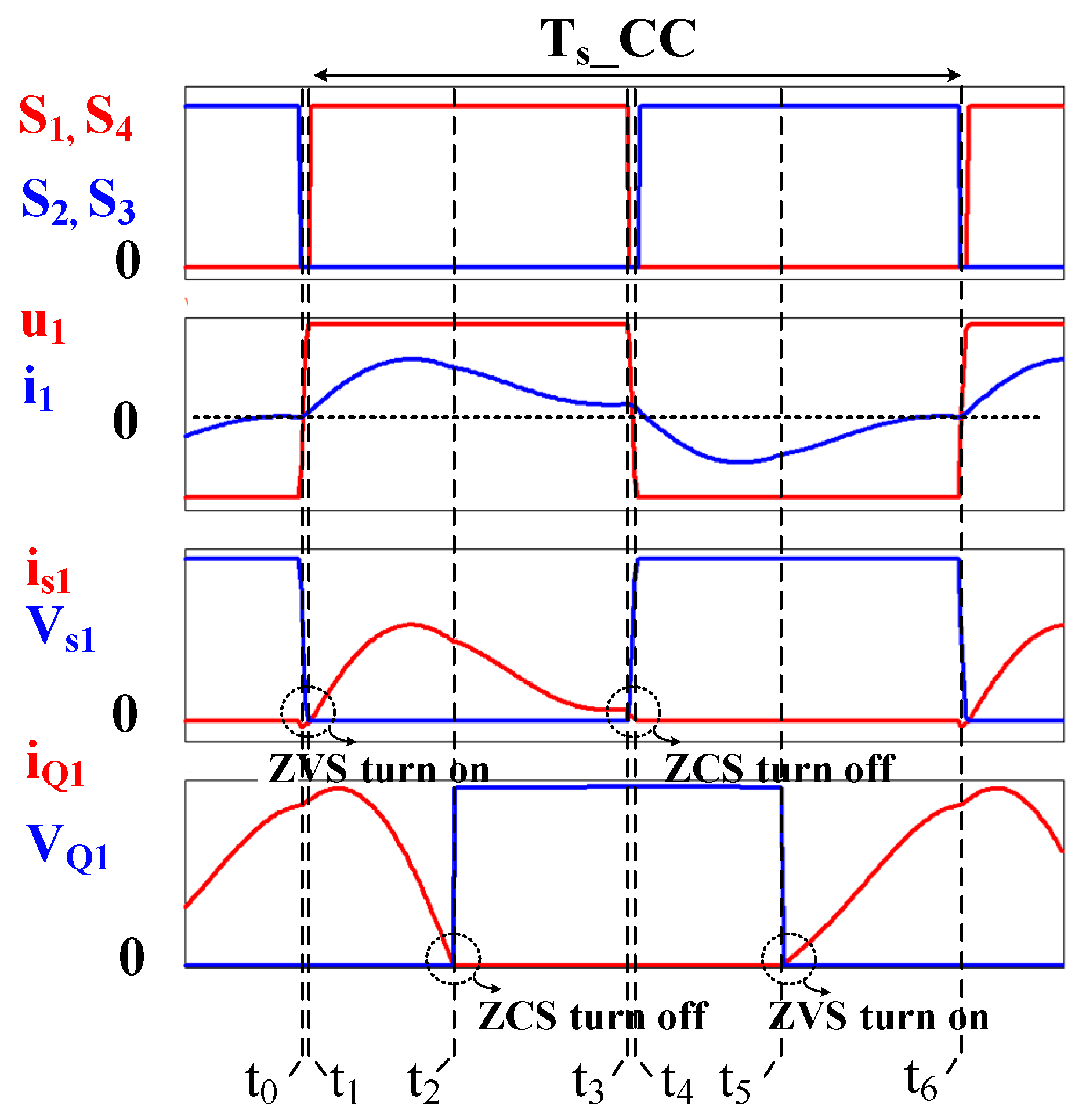
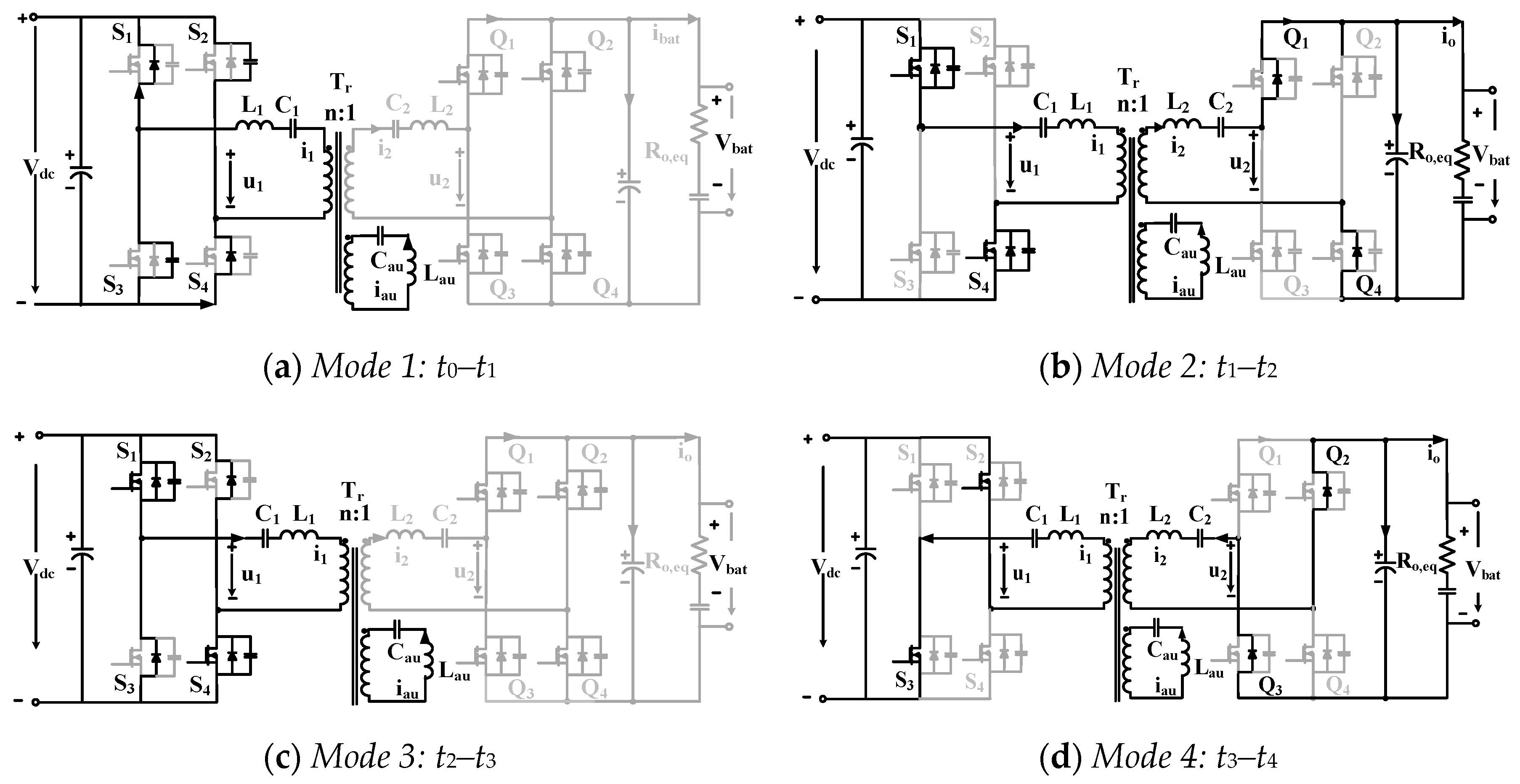
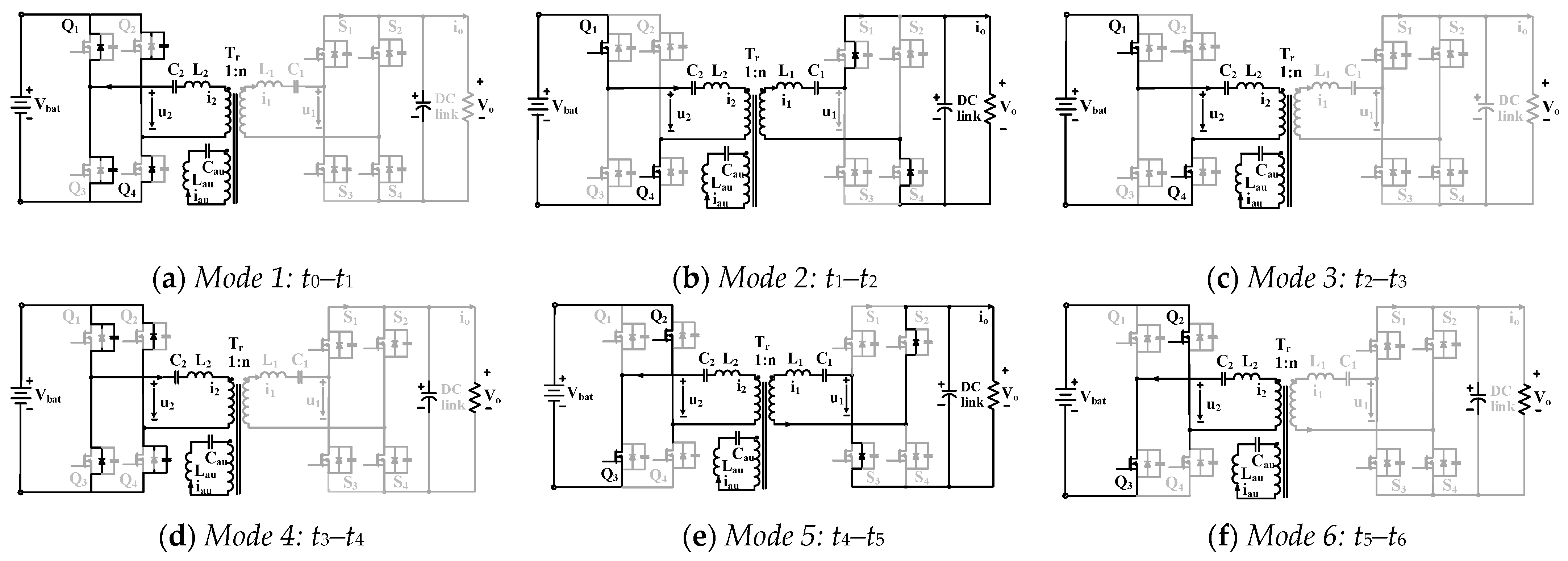
In CC charging mode, the converter completes six distinct operational stages within one switching period.
Figure 13 illustrates the key current and voltage waveforms, while
Figure 14 shows the corresponding circuit diagrams for each mode. In this mode, the converter operates at the resonant frequency
as shown in Equation (16).
Figure 14a: At the beginning of the switching cycle, switches S2 and S3 are turned off under ZCS conditions. No power is transferred to the secondary during this interval. The primary current
discharges the output capacitance of S1 and S4. Once these capacitors are discharged, the body diodes conduct, establishing ZVS for the next switching event.
Figure 14b: S1 and S4 turn on under ZVS. Power begins transferring to the battery through the transformer and synchronous rectifier switches Q1 and Q4. The current
and voltage direction are now positive.
Assuming negligible dead-time, the primary current can be described by:
where
.
Each component used in (12) can be calculated as follows
where
is the voltage across the transformer winding;
is the voltage across
;
is the switching period. In addition, the magnetizing current
and auxiliary current
can be derived as follows
where
At the end of this mode, the primary current meets the total current t , ( + ), which means the end of the resonance operation, which transfers power from the primary side to the secondary side. When the converter operates at , equals to zero.
Figure 14c: As the resonance between
,
, and
concludes, Q1 and Q4 are turned off under ZCS, and Q2 and Q3 are turned on under ZVS. The updated primary current expression becomes:
where
Figure 14d: Switches S1 and S4 turn off under ZCS. Their output capacitances are discharged, followed by conduction through body diodes, preparing S2 and S3 for ZVS operation.
Figure 14e: S2 and S3 are turned on under ZVS. Power is again delivered to the battery, this time via the Q2-Q3 pair, with the current direction reversed from Mode 2.
Figure 14f: Q2 and Q3 are turned off under ZCS, and Q1 and Q4 turn on with ZVS. A new half-cycle power transfer begins, mirroring Mode 3.
The near-ZCS operation demonstrated in experimental results inherently includes parasitic capacitance effects (Coss ≈ 150 pF), with measured turn-off currents remaining below 0.5 A across the operational range. This represents a significant improvement over conventional topologies where parasitic effects typically prevent ZCS achievement under similar conditions.
3.2. Constant Voltage (CV) Charging Mode
In CV mode, the converter continues to operate at the resonant frequency. The main difference lies in the control of output voltage rather than current.
Figure 15 presents the waveform overview, and
Figure 16 depicts the corresponding circuit configurations.
In this mode, the converter operating frequency is below:
Figure 16a: At this point, the primary current is small and consists primarily of the sum of
and
. These discharge the output capacitance of the switches, after which current flows through the body diodes to enable ZVS.
Figure 16b: S1 and S4 turn on with ZVS. Power is transferred to the battery through Q1 and Q4. The direction of the current becomes positive.
Figure 16c: S1 and S4 are turned off with nearly ZCS, and S2 and S3 are prepared for ZVS by discharging their output capacitance.
Figure 16d: S2 and S3 turn on with ZVS, and power is transferred through Q2 and Q3 in the opposite direction.
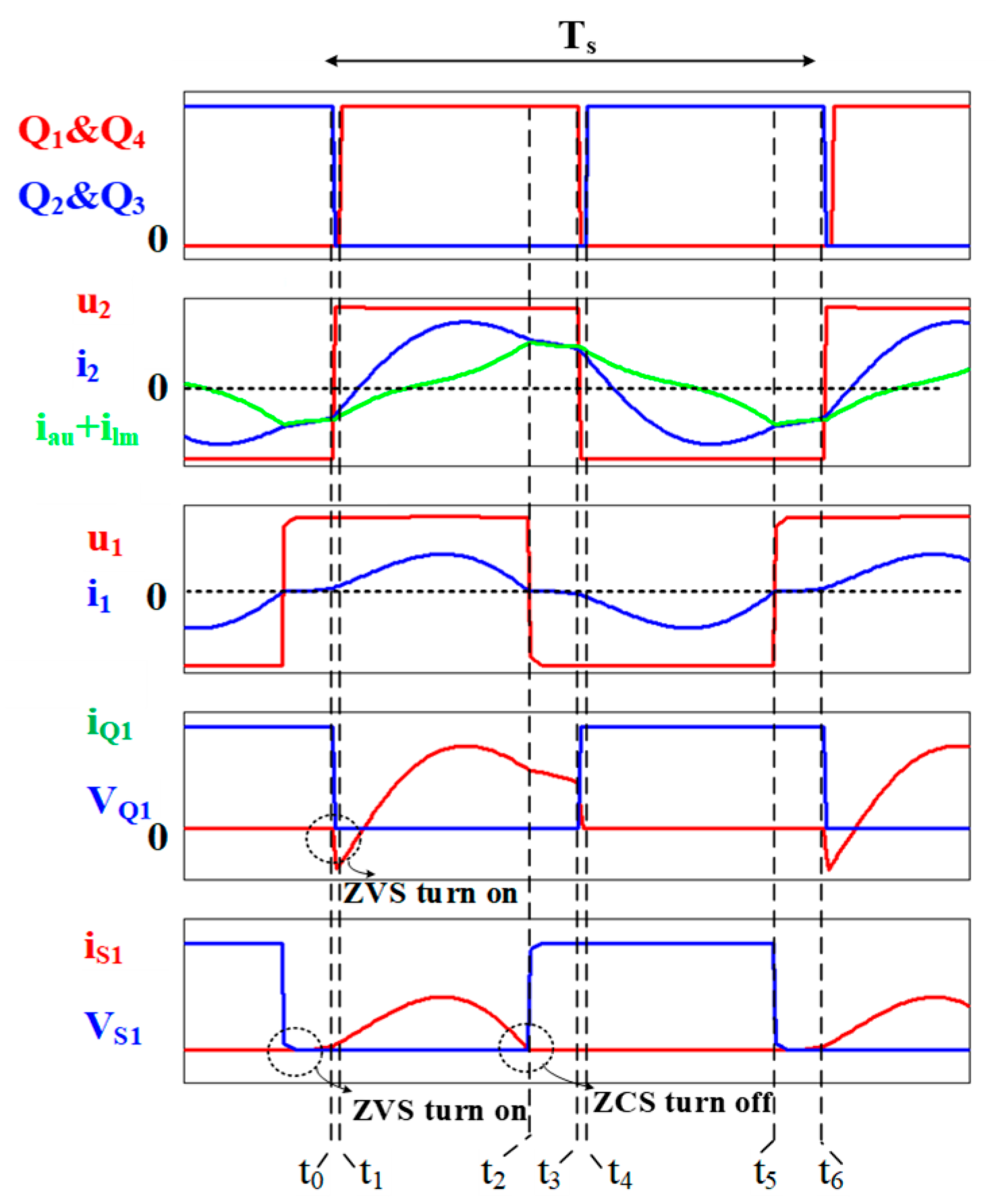
3.3. Discharging Mode
In this mode, the converter operates in reverse, delivering power from the battery back to the DC bus, in return mode. The switching frequency during discharging is modulated between and depending on battery voltage and load conditions.
Figure 17 displays the key waveforms during discharging mode, while
Figure 18 illustrates the six operating stages within one switching cycle.
Figure 18a: At the start of the switching cycle, switches Q2 and Q3 are turned off. The secondary current i2(t) begins charging the output capacitance of Q2 and Q3 and simultaneously discharges those of Q1 and Q4. Once discharged, the current flows through the body diodes of Q1 and Q4, preparing them for ZVS.
Figure 18b: Q1 and Q4 turn on under ZVS. Current i2(t) now flows through the transformer to the primary side. The resonance occurs between
,
, and
, while i2(t) grows and exceeds the sum of the magnetizing and auxiliary currents:
. This mode ends when
equals
, at which point Q1 and Q4 are turned off with ZCS.
Figure 18c: Resonant energy transfer stops. Current i2(t) equals the sum of magnetizing and auxiliary branch currents. Since iS1(t) drops to zero, there is no power transfer to the DC bus.
Figure 18d: This is another dead-time interval. Q1 and Q4 remain off, and i2(t) charges the output capacitances of Q2 and Q3 while discharging those of Q1 and Q4. Once completed, the current flows through Q2 and Q3 body diodes to enable ZVS.
Figure 18e: Q2 and Q3 turn on under ZVS, transferring energy from the secondary side to the primary through the opposite current direction. The waveforms mirror Mode 2 but in reverse polarity.
Figure 18f: The resonance concludes when
. With no further energy transfer, the primary current (t) becomes zero. Q2 and Q3 are then turned off under ZCS, completing the switching cycle.
4. Design Considerations
Based on the previous operational analysis, the proposed converter and traditional CLLLC converter share similar characteristics in their discharging mode across the full voltage range of the EV battery. As a result, the overall design methodology closely aligns with that of the conventional CLLLC converter.
The resonant elements on both the primary and secondary sides , , , and along with the magnetizing inductance , are chosen to meet the voltage gain requirements across the full-load range. Additionally, the auxiliary LC circuit, consisting of and , is introduced specifically to maximize the effective magnetizing inductance , which is critical to ensuring reliable ZVS operation and minimizing switching losses. The resonant frequency is selected such that the converter operates at constant output current during CC charging mode.
4.1. Effective Magnetizing Inductance
A large effective magnetizing inductance significantly reduces the peak turn-off current of the primary switches, thereby lowering the switching loss. To achieve this, the auxiliary inductor
and capacitor
are designed such that the resulting equivalent magnetizing inductance becomes:
The value of the primary current must still be sufficient to discharge the switch output capacitance during dead-time in order to satisfy the ZVS condition. This requirement links the equivalent magnetizing inductance with the maximum switching frequency, dead-time, and output capacitance. Thus, the value of
should fulfill the condition:
where
is the dead-time duration,
Cs is the output capacitance of the switch, and
is the maximum switching frequency.
4.2. Voltage Stress of Auxiliary Capacitor
The auxiliary capacitor
is subject to voltage stress that must be considered in the design. Its peak voltage can be expressed as:
Although the auxiliary branch is designed to resonate with the main magnetizing branch at the same frequency, the value of tends to be smaller than the main resonant capacitors. If selected too small, this can result in excessive voltage across the capacitor. To prevent this, the auxiliary inductor should be chosen such that the total impedance of the auxiliary path remains sufficiently high.
In this work, is selected as approximately half the value of . This balances the reduction of voltage stress on and keeps the core losses in the auxiliary branch at manageable levels, thereby preserving the converter efficiency advantage.
4.3. Soft-Switching Condition in CC Mode
In CC charging mode, the converter is designed to operate at the resonant frequency. To achieve both ZVS and ZCS, the system’s input impedance must have a phase angle of zero at the operating frequency. This ensures that the primary voltage and current are in the phase.
To satisfy this condition, the resonant frequency must be carefully selected such that:
Achieving this ZPA condition not only ensures an efficient energy transfer but also enables robust soft-switching across a wide load range.
4.4. Auxiliary LC Parameter Design and Optimization
The comprehensive sensitivity analysis framework for the auxiliary LC parameters ( and ) begins with a mathematical derivation of sensitivity functions that quantify the relationship between component values and key performance metrics including ZVS range, voltage stress, and overall efficiency, and culminates in resonant frequency tuning where to achieve optimal impedance characteristics. Our analysis demonstrates that auxiliary inductance selection directly impacts the ZVS operational range by 15–20%, while auxiliary capacitance variations influence voltage stress by 10–15%, establishing clear design boundaries for optimal performance. The systematic design methodology starts from fundamental ZVS requirements where , followed by voltage stress constraints ensuring , and culminates in resonant frequency tuning where to achieve optimal impedance characteristics. Multi-objective optimization through a Pareto analysis balances competing requirements of 98.13% efficiency targets, voltage stress limitations below 150 V, and power density exceeding 2.5 kW/L.
The component selection optimization employs comprehensive sensitivity studies revealing 5–8% efficiency improvement potential through optimized frequency tuning, validated through a Monte Carlo analysis that accounts for realistic component tolerances (±5% for inductors, ±10% for capacitors). This probabilistic approach ensures robust design performance across manufacturing variations while maintaining the critical trade-offs between effective inductance enhancement, component stress minimization, and power density maximization. The resulting design methodology provides a systematic framework for auxiliary LC parameter selection that achieves superior soft-switching performance without compromising reliability or practical implementation constraints.
The practical implementation of this design methodology results in specific component requirements. The auxiliary LC circuit requires one 25μH inductor and one 1μF capacitor, adding 85 g (7.1% mass penalty) to achieve 2.75 kW/L power density versus 2.28 kW/L for conventional CLLLC designs. This 20.6% power density improvement, combined with 0.93% efficiency gain and 15% soft-switching range extension, demonstrates superior cost-effectiveness at a USD 45 additional component cost. The volume penalty of 8% is offset by reduced heat sink requirements due to lower switching losses, resulting in net system-level benefits.
5. Experimental Results
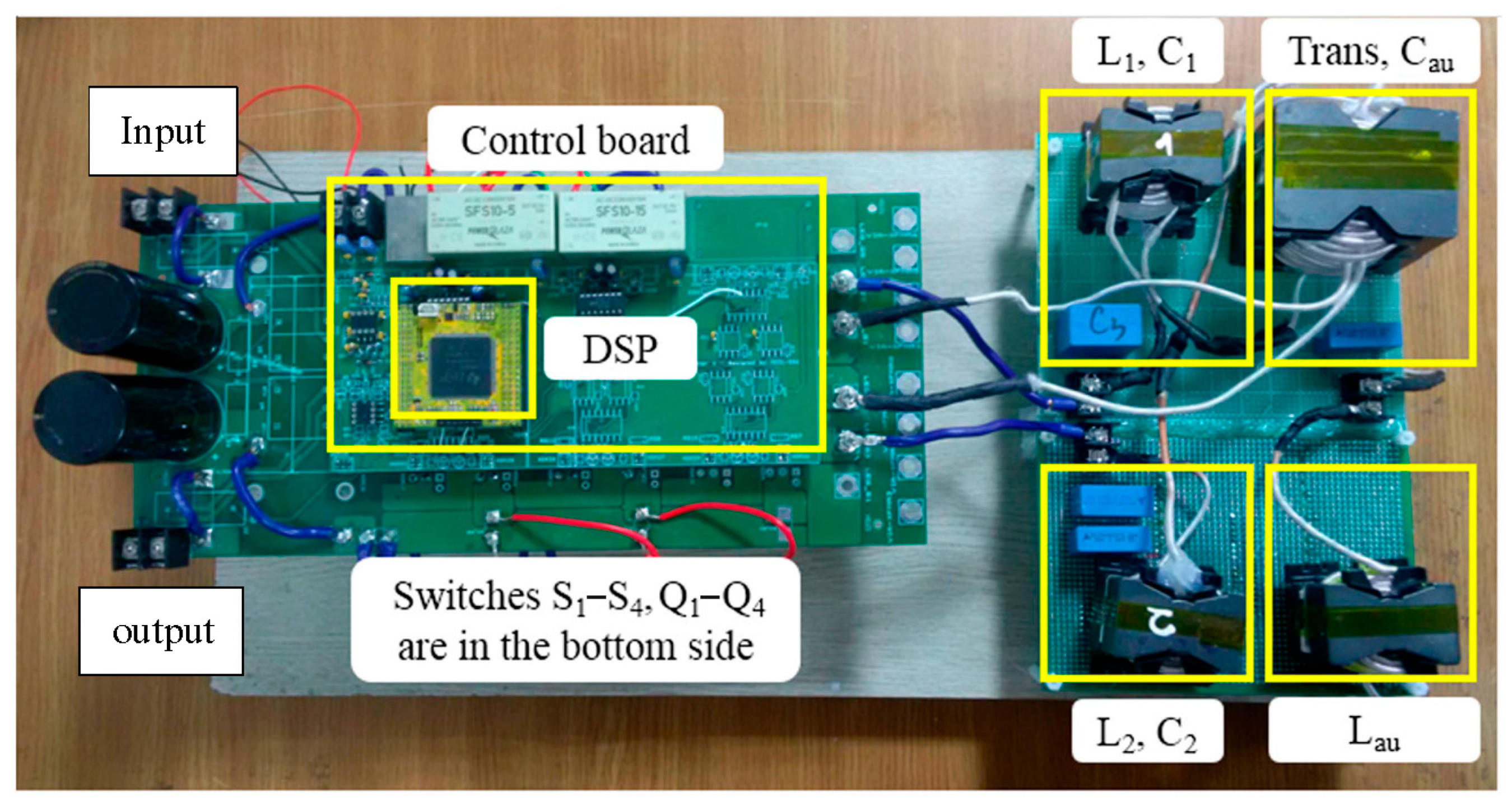
To validate the proposed converter, a 3.3 kW bi-directional resonant prototype was designed and tested under laboratory conditions. The system was tailored for onboard EV charging and V2G operation, supporting both charging (Powering Mode) and discharging (Return Mode). The converter was constructed using a PQ72/54 core transformer with a turn ratio of 16:16.5:16, along with PQ50/50 cores for the resonant inductors. The resonant frequency was set at 59 kHz.
The prototype utilized aluminium-extruded heat sinks with fin configuration to provide natural convection cooling.
Figure 19 shows prototype of the proposed 3.3 kW bi-directional converter with auxiliary LC circuit. The heat sinks were dimensioned to maintain junction temperatures below 100 °C under full load conditions. The thermal resistance from junction to ambient was approximately 2.5 °C/W, enabling efficient heat dissipation from the power MOSFETs and transformer cores without requiring forced air cooling.
The thermal design followed standard power electronics practices with a conservative component selection. The auxiliary inductor (25 μH, ferrite core) operated at a low-flux density ensuring core losses remained below 2 W. The auxiliary capacitor (1 μF, ceramic) experienced minimal ESR losses (<1 W) at 59 kHz operation. Junction temperatures remained within the manufacturer’s specifications through proper heat sink design and natural convection cooling, as evidenced by the stable operation during the extended testing periods.
Table 1 outlines the key specifications of the system, while
Table 2 lists the detailed circuit parameters used in the implementation.
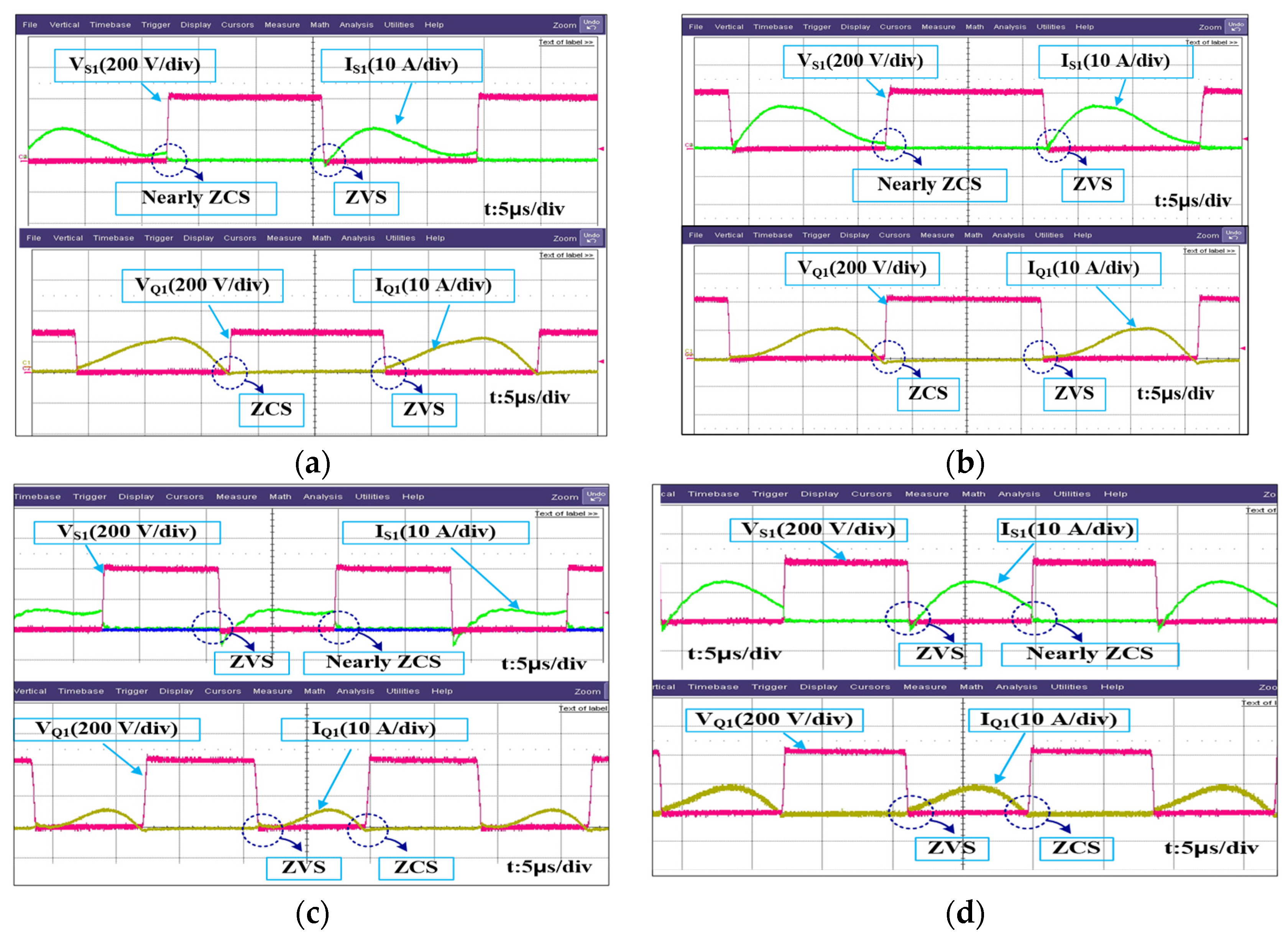
5.1. Converter Operation in the Powering Mode
In this mode, the primary full-bridge inverter switched S1–S4 and drove the transformer, while the secondary side switched Q1–Q4 and operated as a synchronous rectifier. The converter facilitated a two-stage battery-charging profile: CC followed by CV, as depicted in
Figure 20.
During CC mode, a stable output current was delivered to the battery as its terminal voltage increased. Once the battery voltage reached the set point, the CV mode began, and the output current gradually decreased while maintaining a Constant Voltage. This transition ensured safe and efficient charging.
Waveforms shown in
Figure 21 and
Figure 22 verify the performance under both partial and full load. At 57% and 100% load in CC mode, the converter operated precisely at its resonant frequency. All primary switches demonstrated ZVS turn-on and near-ZCS turn-off, while the secondary switches achieved full ZVZCS conditions. In CV mode, the converter continued to operate with minimal switching losses, aided by the enhanced effective magnetizing inductance provided by the auxiliary LC circuit.
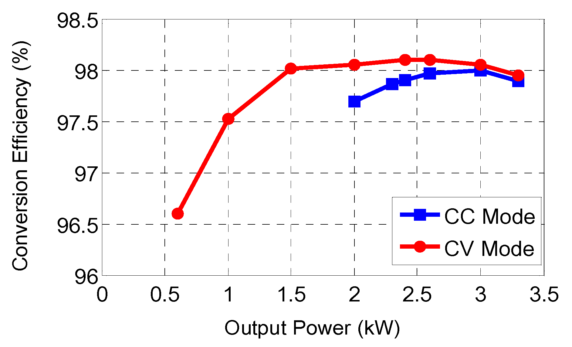
The measured efficiency results, shown in
Figure 23, reveal a peak efficiency of 98.13% at 2.3 kW in charge mode with an input voltage of 400 V. Even under light load conditions, efficiency remained above 96%.
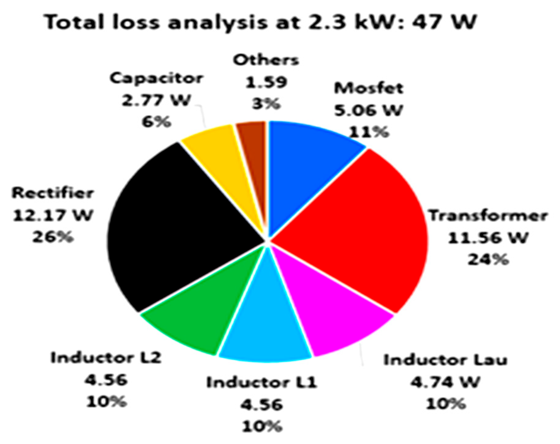
Figure 24 provides a breakdown of power losses, with the majority originating from the rectifier diodes and magnetic components. The auxiliary circuit contributed significantly to reducing primary side losses by lowering circulating currents and enabling soft-switching across the load range.
The CV mode demonstrated higher efficiency compared to the CC mode due to several factors: (1) At a Constant Voltage operation, the converter operated closer to the resonant frequency, reducing reactive power circulation; (2) the effective magnetizing inductance was maximized in CV mode, reducing turn-off switching losses; (3) lower RMS current values in CV mode resulted in reduced conduction losses in both primary and secondary circuits. The efficiency improvement ranged from 0.3% to 0.8% across the load spectrum, with the maximum benefit observed at partial loads where the soft-switching margins were most pronounced.
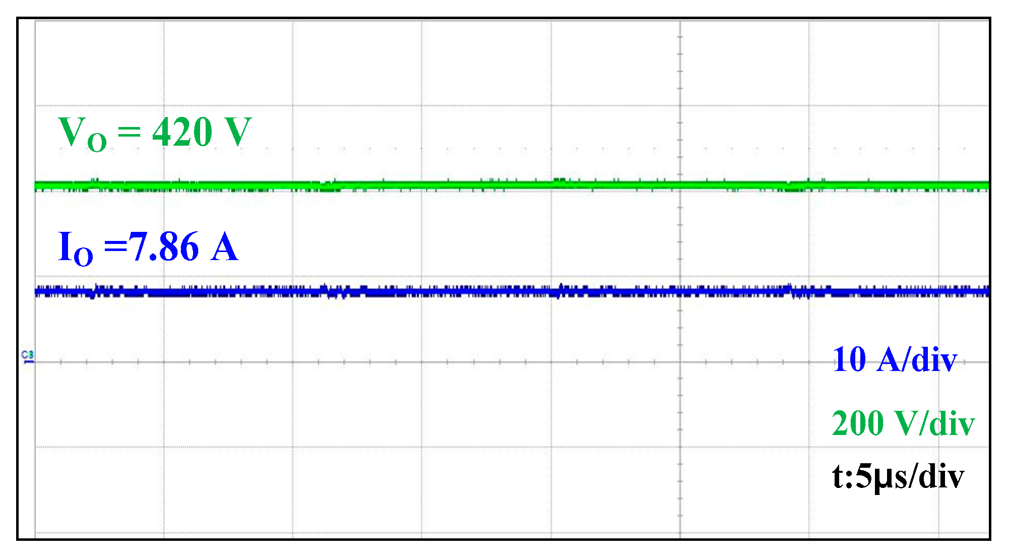
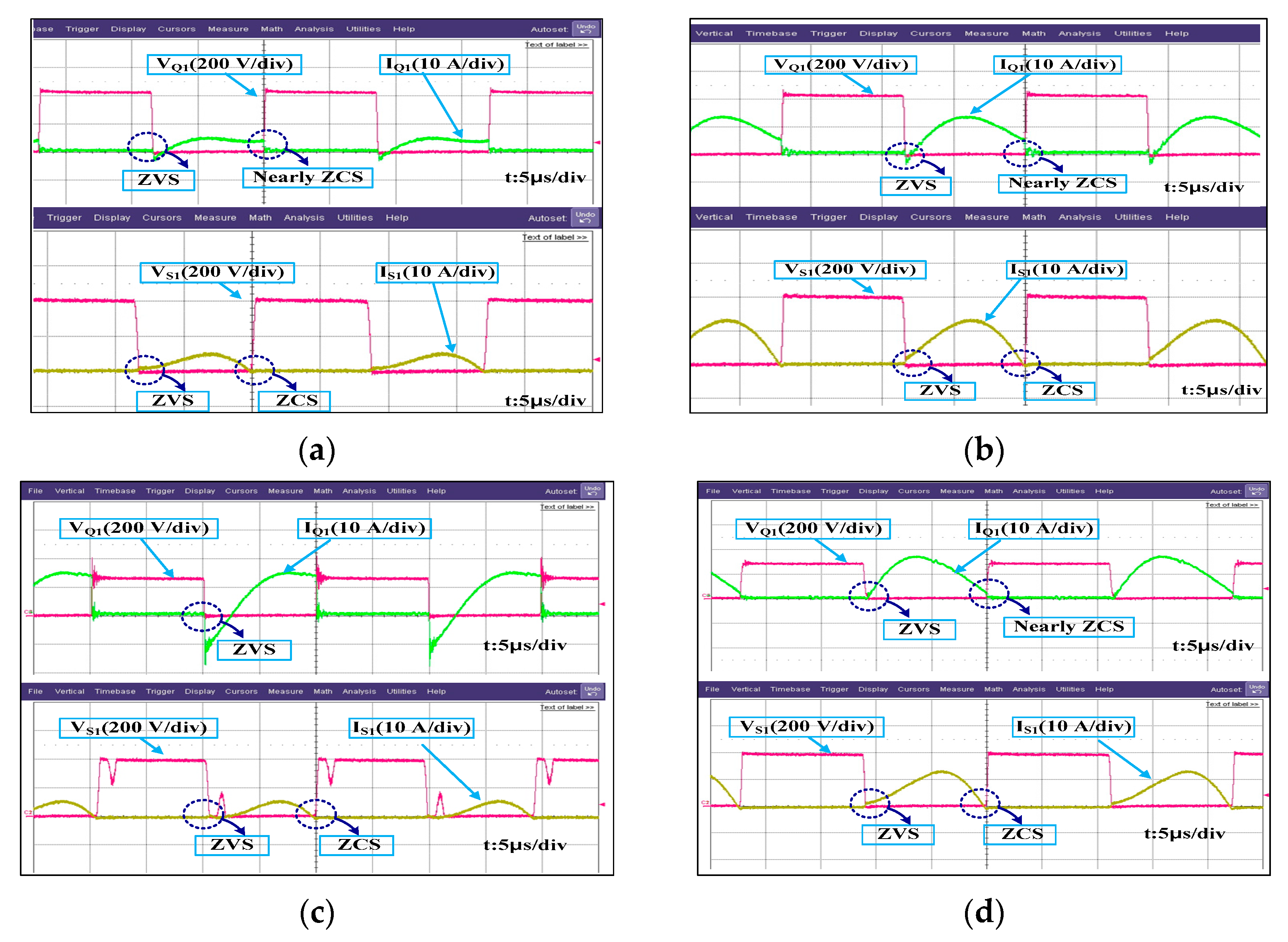
5.2. Converter Operation in the Discharge Mode
In the Return Mode, the converter transferred energy from the battery back to the DC bus. In this configuration, the secondary switches (Q1–Q4) operated as controlled switches, while the body diodes of the primary switches (S1–S4) functioned as rectifiers. Comprehensive experimental validation was performed to verify the converter’s bi-directional capability and efficiency in this critical V2G mode.
Waveforms in
Figure 25 illustrate converter behavior at different load levels and input voltages (
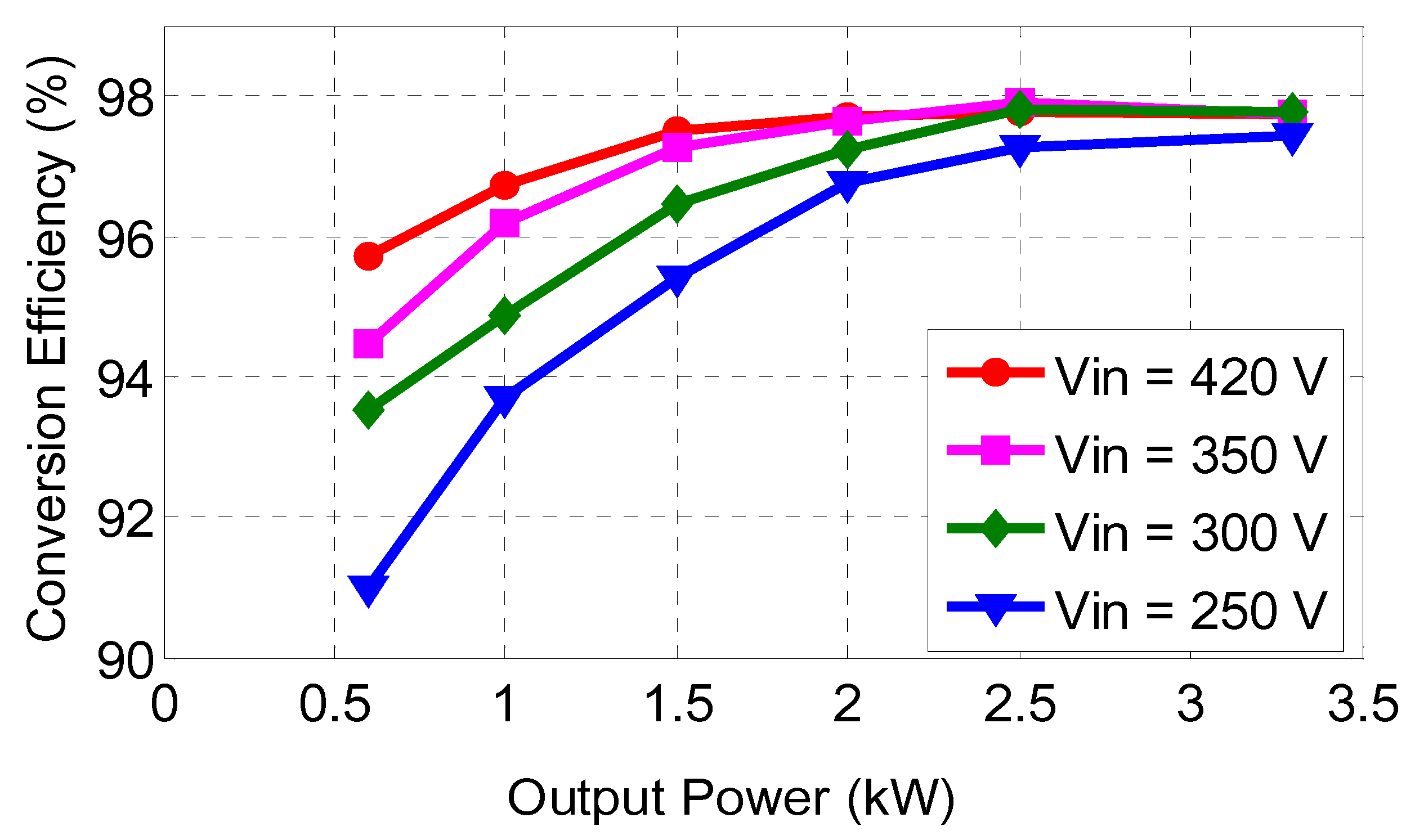
= 250 V and 420 V). At higher voltages and full loads, the converter achieved both ZVS and near-ZCS conditions. Under lighter loads and lower battery voltages, ZVS was maintained, while ZCS may not have been fully achieved due to the reduced energy available for resonant transitions. However, thanks to the high effective magnetizing inductance, even these conditions resulted in lower turn-off currents than conventional CLLLC converters.
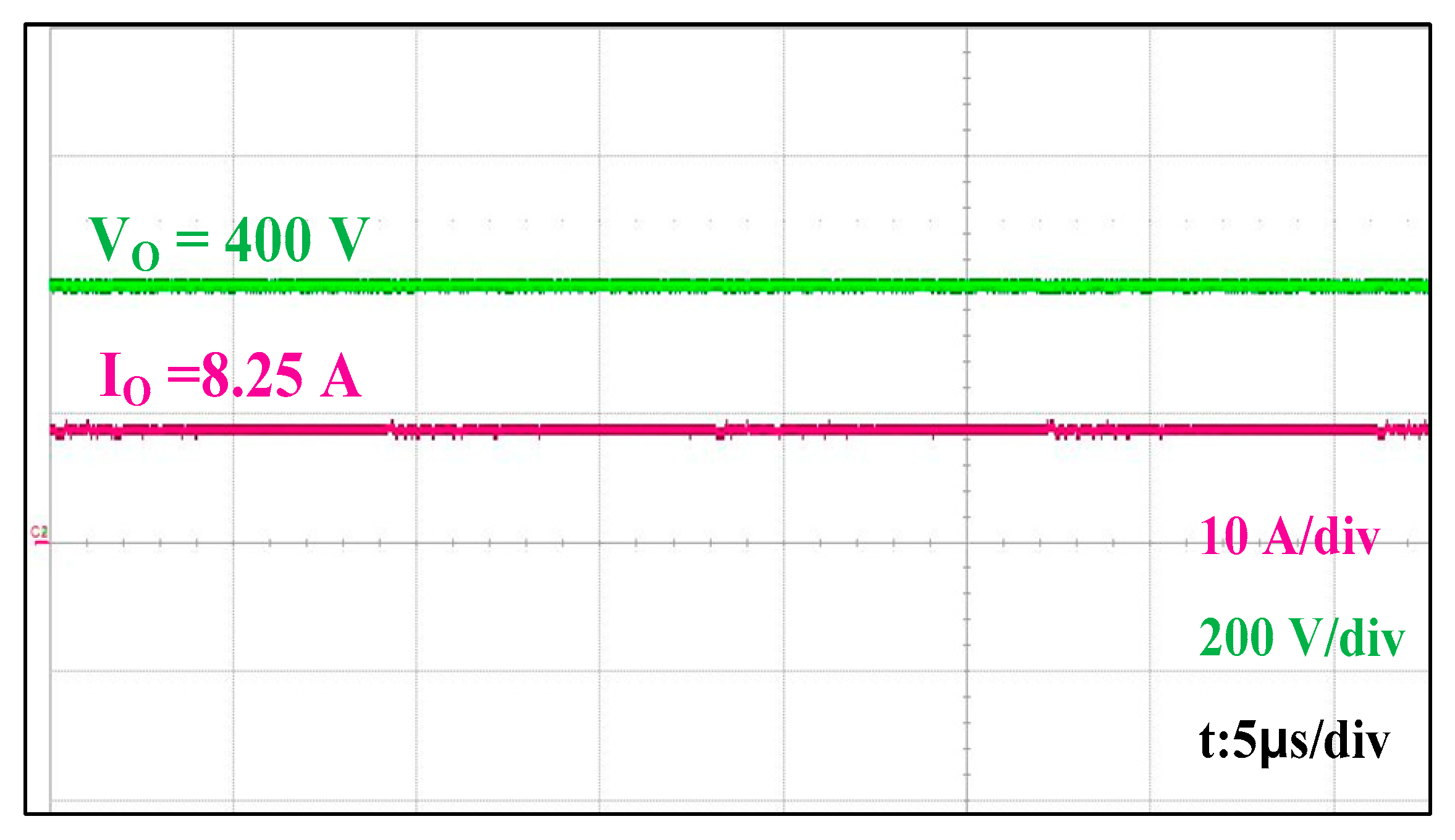
The output voltage and current waveforms shown in
Figure 26 confirm a steady operation at a full load. Efficiency data in
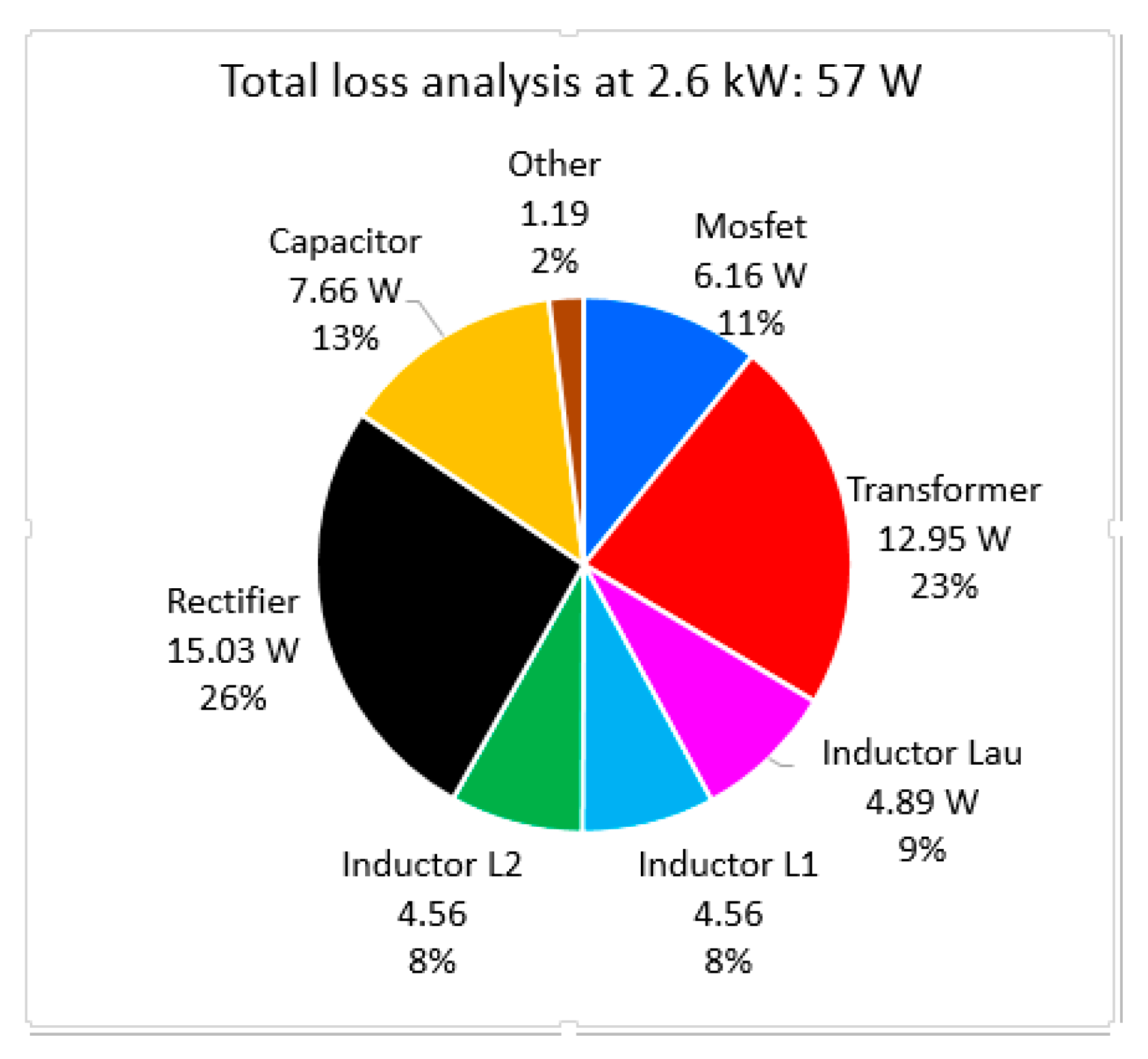
Figure 27 indicates a peak of 97.9% at 2.4 kW, with only a slight drop observed at lower voltages due to increased circulating losses. These results demonstrate the converter’s excellent performance in both energy delivery directions, validating its suitability for V2G applications. The loss breakdown in
Figure 28 shows that the converter maintained balanced efficiency by minimizing switching losses across both sides of the circuit, confirming the design advantages of the auxiliary LC configuration for bi-directional operation including both charging and discharging modes.
5.3. Performance Benchmarking
The experimental comparison demonstrated clear advantages of the proposed topology over conventional DAB with TPS modulation. The 0.33% efficiency improvement (98.13% vs. 97.8%) translated to 11 W reduced losses at full load, achieved through enhanced soft-switching across 85% of the load range versus 70% for DAB topology.
Frequency stability represented a critical advantage for V2G applications, with the proposed converter maintaining ±5% variation compared to ±25% for DAB with TPS. This narrow frequency band simplified the EMI filter design and enabled predictable grid synchronization behavior through the auxiliary LC circuit’s optimal impedance characteristics.
The 31% switching loss reduction (12.5 W vs. 18.2 W) directly correlated with extended ZVS range and improved soft-switching conditions, while the dynamic response achieved <50 ms settling times versus 75 ms for DAB with TPS. This superior transient performance stemmed from simplified single-parameter control versus three-parameter TPS optimization, reducing computational overhead and enabling a faster control loop response.
A control complexity comparison revealed significant practical advantages: while DAB with TPS required sophisticated algorithms managing three independent phase-shift parameters, the proposed converter achieved superior performance through straightforward auxiliary LC parameter tuning, substantially reducing implementation complexity for real-time control systems.
A comparative performance analysis of proposed CLLLC vs. DAB with triple-phase-shift is shown in
Table 3 below.
6. Conclusions
This paper has proposed a high-efficiency bi-directional CLLLC resonant converter incorporating an auxiliary LC circuit through a tertiary transformer winding, specifically tailored for Vehicle-To-Grid (V2G) systems. The key advantage of the proposed topology lies in its ability to achieve soft-switching—ZVS at turn-on and near-ZCS at turn-off—across a wide range of operating conditions, without requiring significant variations in switching frequency.
By leveraging the auxiliary LC network, the converter dynamically enhances the effective magnetizing inductance, which enables efficient operation in both Constant Voltage (CV) and Constant Current (CC) modes at distinct fixed frequencies. This innovation not only minimizes switching and conduction losses but also suppresses circulating currents that typically degrade performance in conventional CLLLC converters.
A 3.3 kW experimental prototype was developed to validate the proposed approach. The measured results confirm high performance in both charge and discharge modes, with peak efficiencies reaching 98.13% and 98%, respectively. The proposed auxiliary LC approach successfully addresses the key limitations of conventional CLLLC converters in bi-directional applications, delivering measurable improvements despite the additional component requirements and design complexity. The experimental validation confirms that the quantified benefits including enhanced efficiency, extended soft-switching range, and improved power density substantially justify the implementation trade-offs for high-performance V2G applications. These outcomes highlight the suitability of the proposed converter for modern EV onboard charging systems, where high efficiency, power density, and bi-directional operation are essential.


