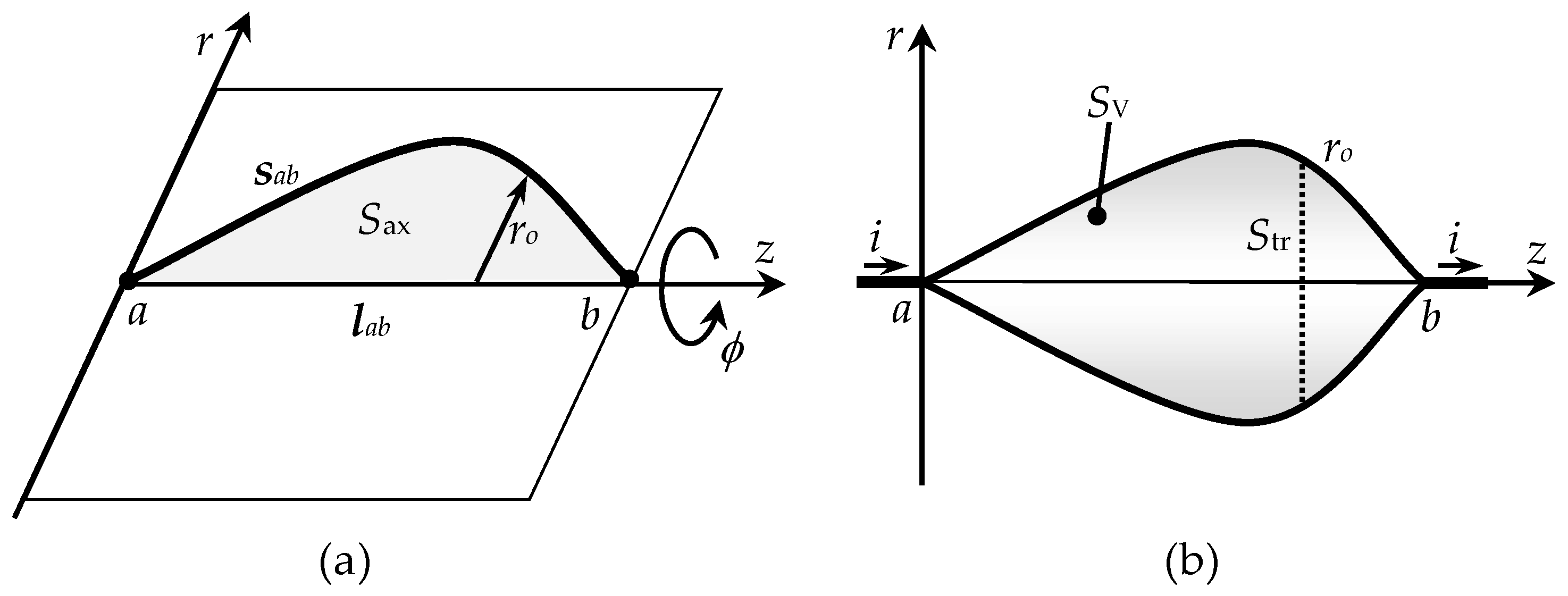
However, as we shall see, the results are rather different for high-frequency regimes.
There is also another difference worth noting. In the case of the cylindrical wire, the boundary surface SV is fully conductive and establishes a well-defined flux tube for the current (conduction current). That is not exactly true in the case of the parallel plate capacitor, where fringing field effects take place around the plates, notably at the edges near the boundary r = ro; in other words, the displacement current flowing between the plates is not entirely contained in a well-defined cylindrical flux tube.
Electrostatic fringing field effects in parallel plate capacitors are responsible for the undesirable nonuniformity of the E-field between the plates, with nonuniformity being determined by two main factors: on the one hand, the dielectric core permittivity relative to the external medium permittivity and, on the other hand, the residual electric charge Qe on the edges and external faces of the capacitor plates.
Higher relative permittivity values lead to a strong confinement of the E-field inside the dielectric core and an increase in the electric charge Q on the internal faces of the capacitor plates and, therefore, imply a reduction of the Qe/Q ratio.
Ordinarily, these effects are assumed to be negligible. We will adopt the same assumption, which is applicable when the dielectric wafer is very thin, h << ro, as needed to obtain high values of the capacitance CDC in (34).
4.1. Base Lossless Case (PD-PC)
As a first step, we consider that losses are absent. The dielectric medium is a perfect electric insulator with real ε and σ = 0, and the capacitor plates are perfect electric conductors with .
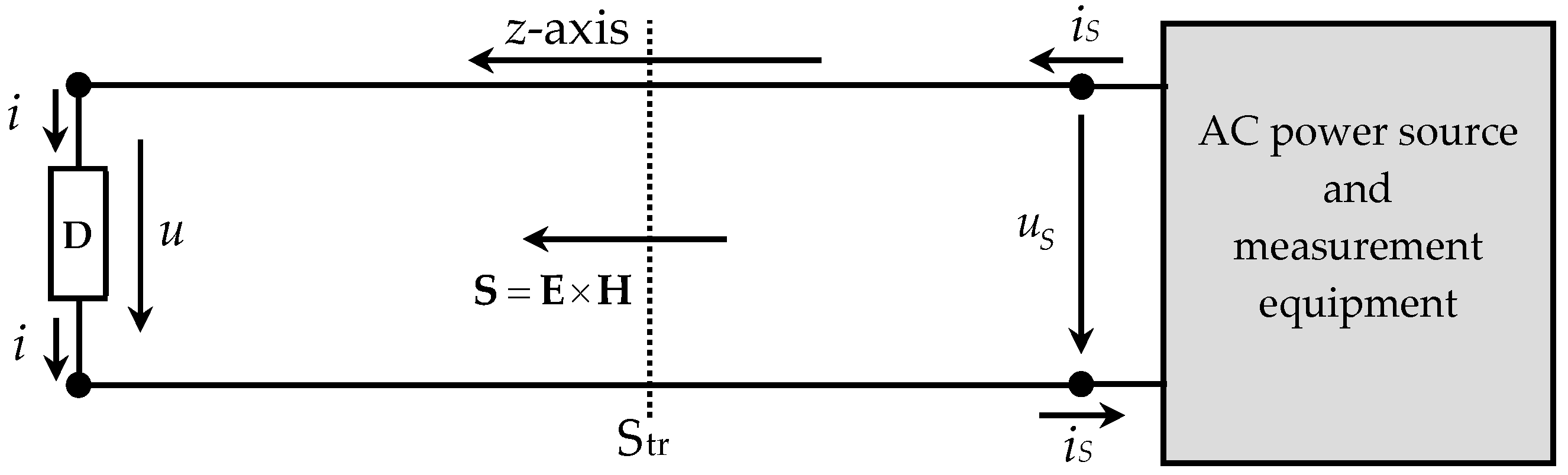
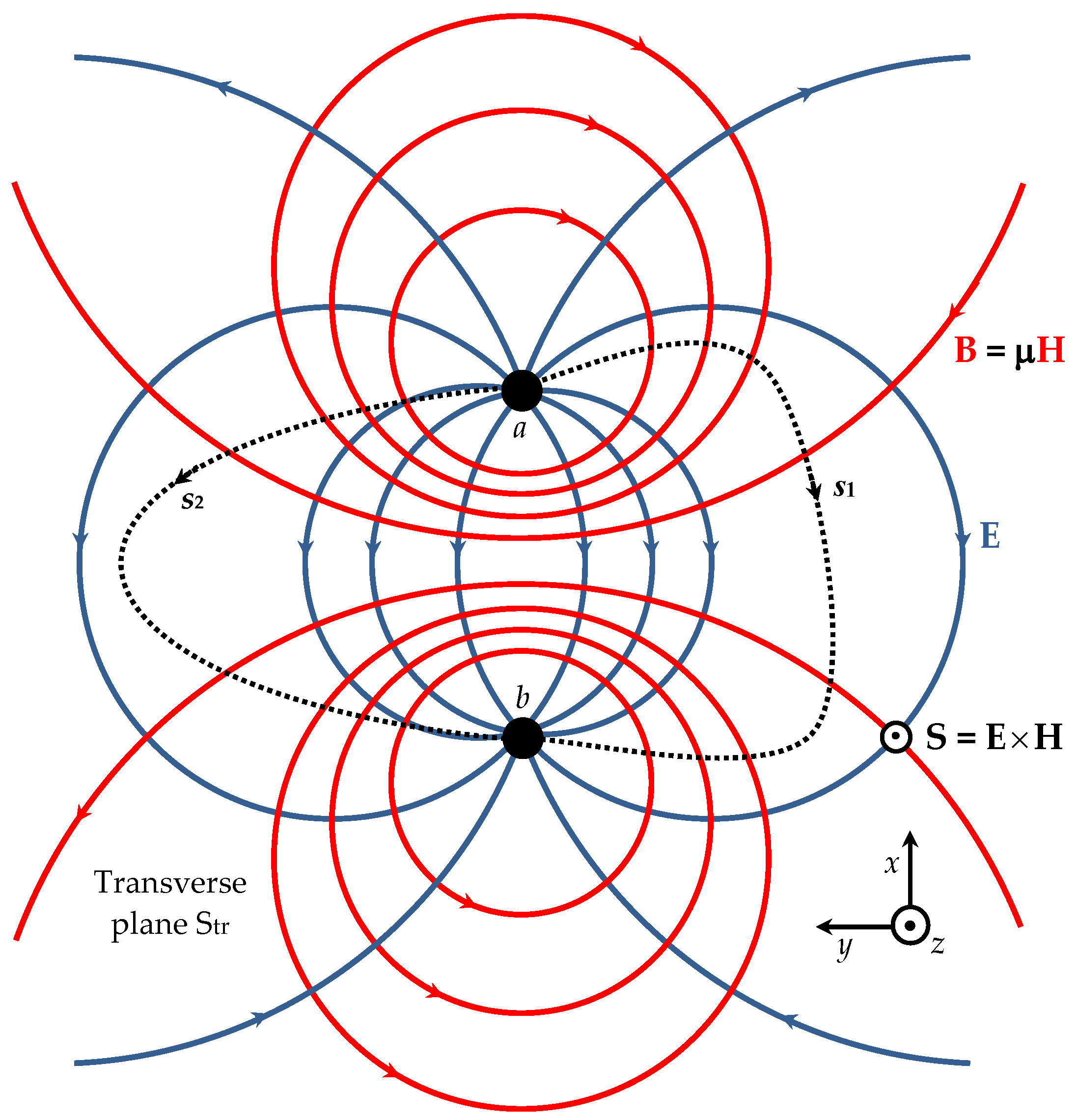
The device voltage is calculated by integrating the E-field along the peripheral path
aa1a2b2b1b, which is indicated by a broken line in
Figure 6.
By plugging
from (35) into (36), and dividing the latter by the current, we obtain the device impedance, as follows:
where
v denotes the speed of light in the dielectric medium of permittivity
ε. Note in (37) that the term
tends toward 2 when
, which confirms the low-frequency result in (34), valid when
.
The result in (37) can be confirmed using the energy-based definition in (22) that involves the inward flux of the complex Poynting vector through the device’s boundary surface S
V. In fact, we have:
where the E-field and the Poynting vector are zero in the circular PEC plates.
For the lossless case, the complex power
is purely imaginary (reactive power), and from the complex Poynting theorem we must have:
The time-averaged magnetic energy stored in the dielectric volume is computed using
in (35), yielding the following result:
Likewise, the time-averaged electric energy stored in the dielectric volume is computed using
in (35), yielding the following result:
The interested reader may check
Appendix A for details on integrals involving the squared Bessel functions
such as those appearing in (40) and (41).
Finally, by subtracting the two energies, and employing (39), we find:
which confirms (37). We believe that the utilization of the energy formalism in (38)–(42) for evaluating the device impedance is a novel contribution, the advantage being that the concept of voltage is not involved.
We may confirm that, in the limit case ρ << 1, the general results for the time-averaged magnetic and electric energies in (40) and (41), yield the familiar low frequency results and . Let us check.
For
ρ << 1, by using the first two terms of the series expansions of the Bessel functions, the following approximations apply:
By substituting (43) into (40) and (41) and considering
we see that
The equations in (35) express the electric and magnetic fields in terms of the device current; however, if convenient, they can be rewritten in terms of the device voltage. All we have to do is replace
with
and use
from (37). This yields the following field equations:
The frequency behavior of
in (37) is determined by the zeros
of the
J0 and
J1 Bessel functions, which are as follows [
12,
16]:
from where an ordered sequence of critical frequencies
fk can be identified, the first of which is denoted by
fc, that is:
where
v0 is the free-space speed of light, and
is the relative permittivity of the dielectric core of the capacitor. While the zeros of
J0 (odd
k) identify short-circuit conditions
the zeros of
J1 (even
k) identify open-circuit conditions
; hence, we have:
The critical frequencies above, which are determined by the geometrical parameter ro, are resonance frequencies for which no energy can flow into the device; in fact, for the time-averaged values of the electric and magnetic energies stored in the dielectric core of the device are exactly balanced, , and the complex power is zero.
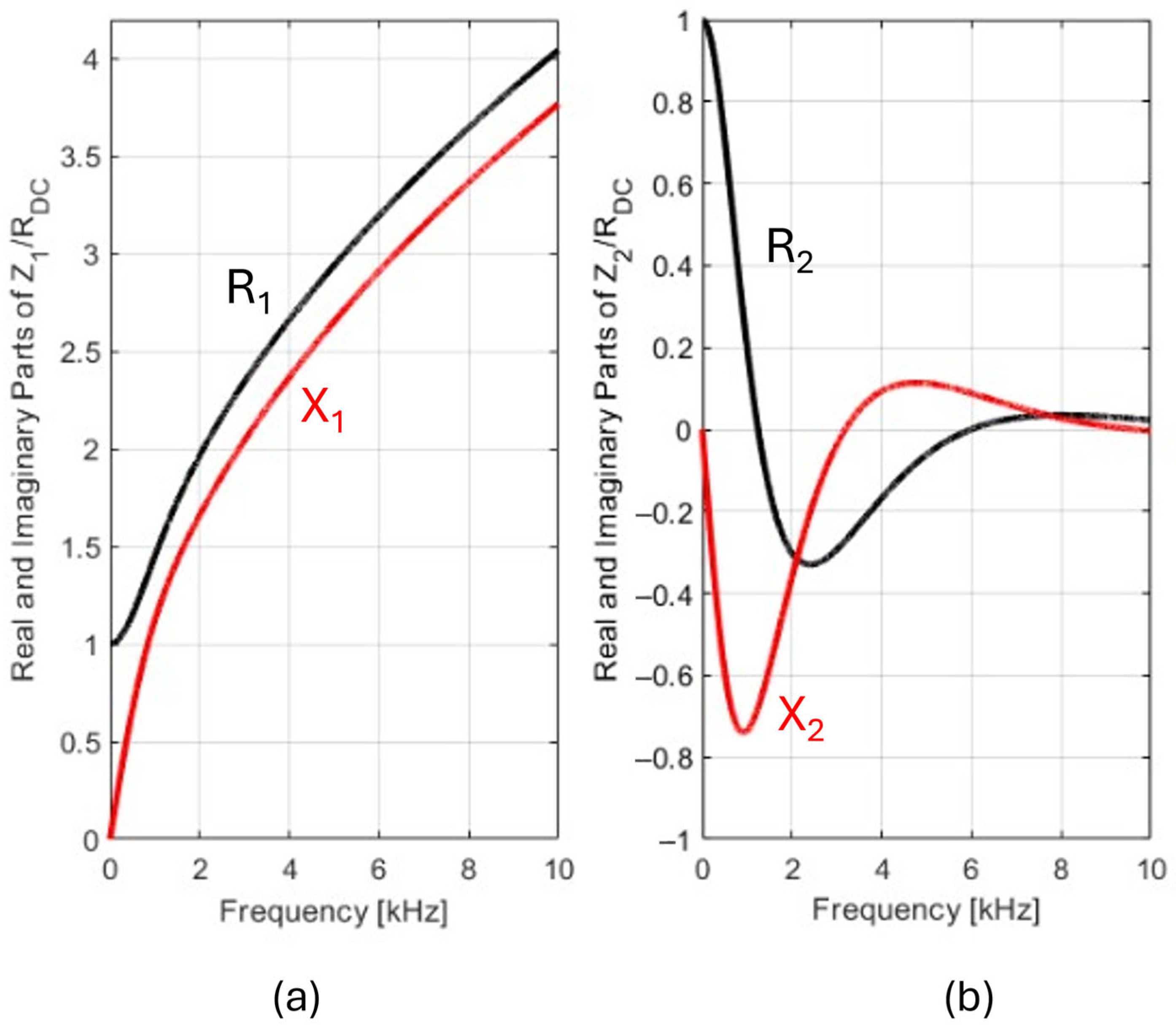
According to low-frequency analysis, it would be expected from (34) that the behavior of the device would always be capacitive, with its impedance decreasing monotonically to zero as the frequency increases to infinity, . Now, we realize that this is not true. The device impedance is capacitive in the range of 0 < f < fc, zero at f = fc, becomes inductive in the range of fc < f < f2, increases to infinity at f = f2fc, returns to capacitive behavior in the range of f2 < f < f3, and so on, repeatedly.
The modulus and angle of impedance,
, in (37), for the lossless case (reference base case), are plotted against the frequency in
Figure 7, considering the frequency window of 0–15 GHz and employing the following data:
As expected, it can be seen that the first critical frequencies are f1 = 7.257 GHz, where = 0, and f2 = 11.56 GHz, where The impedance angle jumps between two constant values, −90° and +90°.
If we had chosen to graph the device’s admittance, the singularity would appear at f1, and the zero would appear at f2.
4.2. Lossy Dielectric and Lossless Plates (ID-PC)
The inclusion of dielectric losses in impedance calculations is formally very simple; we only have to replace the (real) permittivity with a complex permittivity, adding to the first a new imaginary part
Let us go back to the original concept of complex conductivity
which was introduced in
Section 3, and write:
where
υ represents the so-called loss factor or loss angle.
Then, by using the complex
in (37), we obtain the following result:
We emphasize that the argument of the Bessel functions is now complex (fourth quadrant). The zeros and infinite values mentioned in the analysis of the lossless case no longer appear. Resonance phenomena still occur at frequencies close to those in (47), but the flow of energy into the device is not zero: .
Although the insertion of
into
is technically simple, the specification of the complex function
is not trivial. It depends on the physical–chemical composition of the medium responsible for the diverse polarization mechanisms (dipolar, ionic, atomic, and electronic) at play, each of which has its own signature and its own critical frequency. The real and imaginary parts of the analytic function
are interdependent and, owing to causality, have to obey the Kramers–Kronig relationships [
17].
Often, to make the analysis easier, the parameters
and
are assumed to be constant. Here, however, we will adopt a frequency-dependent model which, in any case, is the simplest of all, the Debye model [
17]:
where
denotes the relaxation frequency of the dielectric medium.
In this research, the following data are used:
and
fr = 400 GHz. Close to the device’s critical frequencies
f1 and
f2 the loss angle of the dielectric is about 15 mrad. Graphical results for the modulus and angle of the device’s impedance in (51) are shown in
Figure 8 (solid lines labelled 1).
Although an echo of the infinite impedance spike in
Figure 7 can still be observed in
Figure 8 (peak about 14 Ω for
f close to
f2), it is clear that the presence of dielectric losses can effectively smooth out the resonance singularities predicted for the lossless case.
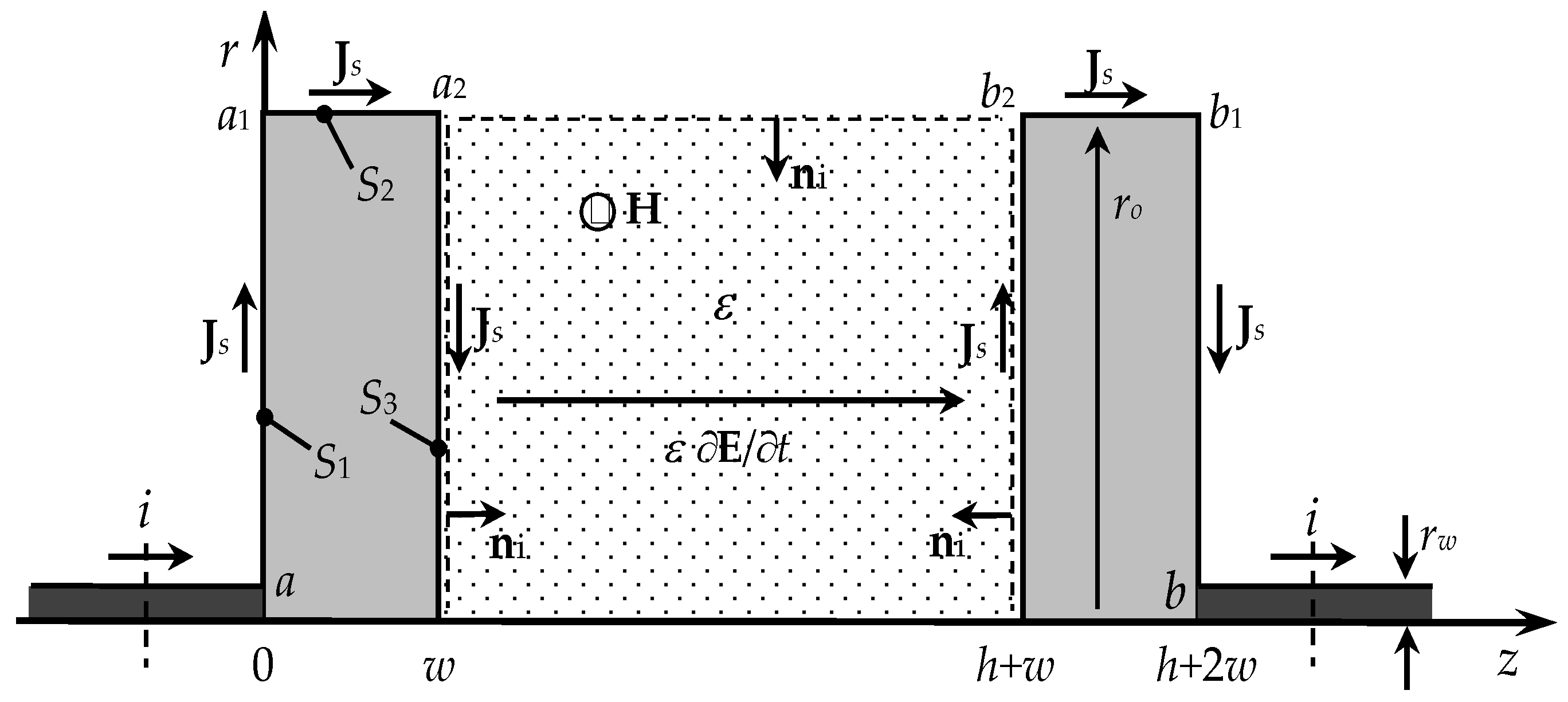
4.3. Lossless Dielectric and Lossy Plates (PD-IC)
The electric and magnetic fields are zero inside the capacitor’s PEC plates. Outside, just near the plates’ boundary surface, the tangential E-field remains zero. However, that is not true of the tangential magnetic field, which, according to
will not be zero if a current sheet
JS flows in an interface perpendicular to
H. The subtraction of the tangential
H fields on both sides of the current sheet must equate the intensity of the latter [
1,
8], that is:
.
Let
JS denote the linear current density (A/m) of the sheets of current flowing in the various parts of the plates. Due to symmetry, it will suffice to analyze one of the two plates, the left one in
Figure 9, for 0 <
z <
w, whose closed boundary is
Consider a generic circle of radius
r (0 <
r <
ro) in the circular interface
S1, at
z = 0, where a radial sheet of current exists
Also, keep assuming that fringing field effects are negligible small (no electric charge on
S1). Then, the EM field tangential to
S1 is given as follows:
Consider the cylindrical interface
S2 of radius
ro and thickness
w where an axial sheet of current exists
Then, the EM field tangential to
S2 is given as follows:
Finally, consider a circle of generic radius
r (0 <
r <
ro) in the circular interface
S3, at
z =
w, where a radial sheet of current exists
Also, remember that
S3 contains a radial distribution of electric charge characterized by a surface density
εE(
r), where
E is the axial electric field in (35). Then, the EM field tangential to
S3 is given as follows:
where
Regarding the result in (55) for
S3, which was obtained with the help of (35), we emphasize that the sheet of conduction current is radial inward at the periphery, with a density of
but zero at the center. The reason that this happens is the gradual conversion of the plate conduction current sheet into axial displacement currents.
However, the conversion is not necessarily monotonic. Recalling that in (46) is the first zero of the Bessel function J1, it can be assured that if , then the current in S3 will, in fact, be inward radial, because the ratio , in (55), is positive for every possible value of r. Now, consider the case then for , the ratio is positive again; however, on the contrary, for smaller values of r, such that , the ratio turns negative, and the current will become outward radial.
The results for
in (53)–(55) for the PEC case are key for the calculation of the electric field in the plates when losses are taken into account, i.e., when the plate conductivity
σp is finite. The field penetration depth
δ, and the surface resistance
Rs of the conductive plates are defined as usual in skin effect analysis, through:
Although the plates are not PEC, we may still assume that the plate conductivity is high enough to guarantee that the new situation can be treated as a perturbation of the original PEC problem. In other words, we consider the following approximations:
- -
The plates are thick, undergoing a strong skin effect, δ << w;
- -
The H-field tangential to the boundaries S1, S2 and S3 is equal to the non-zero H-field in (53)–(55);
- -
The zero E-field in (53)–(55) can be recalculated from the corresponding H-field in
Sk using the following relationship, from skin effect theory [
1]:
Therefore, along the various segments identified in
Figure 9, we can write:
Next, we proceed with the evaluation of the device impedance, taking into account the perturbation caused by the skin effect on the lossy plates. We integrate the E-field along the peripheral path
aa1a2b2b1b (
Figure 9) and divide the result by
. This yields:
The skin effect impedance perturbations
above are easily determined from
and
, in (58), as follows:
The term in (59) is the voltage between the inner faces of the plates, between the peripheral points a2 and b2. Its calculation is more elaborate because we do not know the E-field between those points for the non-PEC case.
Consider the application of the complex Poynting theorem to the lossless dielectric wafer (dotted region in
Figure 9) sandwiched between the lossy plates. Energy flows radially into the dielectric across the cylindrical surface of radius
ro and length
h (where
is defined); flows in the axial direction toward the plates across the circular tops of radius
ro at
z =
w and
z =
h +
w; and is also stored in the dielectric volume in the form of electric and magnetic energy. Hence, we must have:
With regard to the right-hand side of (61), the term is the same as in (40); however, strictly speaking, the term is not the same as in (41).
The stored electric energy in (41), for the PEC plate case, was evaluated solely using the axial electric field: . However, when lossy plates are considered, a radial E-field component parallel to the plates must be added. The total E-field inside the dielectric medium is elliptically polarized, and consequently, its rms value will be such that . Nonetheless, for good conducting plates, the term is several orders of magnitude smaller than ; therefore, according to (39), we may say that the right-hand side of (61) is practically coincident with .
Therefore, we can rewrite (61) as follows:
or
The integral involving
in (63) is not new; we encountered it in (40). By using this integral in (63), we obtain:
For the limit case ρ << 1, the term inside the large parentheses tends toward 1/4, and we find the low-frequency approximation .
The contributions
in (60), together with
in (64), fully characterize the frequency-dependent impedance corrections due to the presence of strong skin effect in the imperfect plates of the device. Adding them, we find:
where the influence of the frequency is conveyed in
and
.
Finally, from (59), the device impedance, with lossless dielectric but lossy plates, is computed as follows:
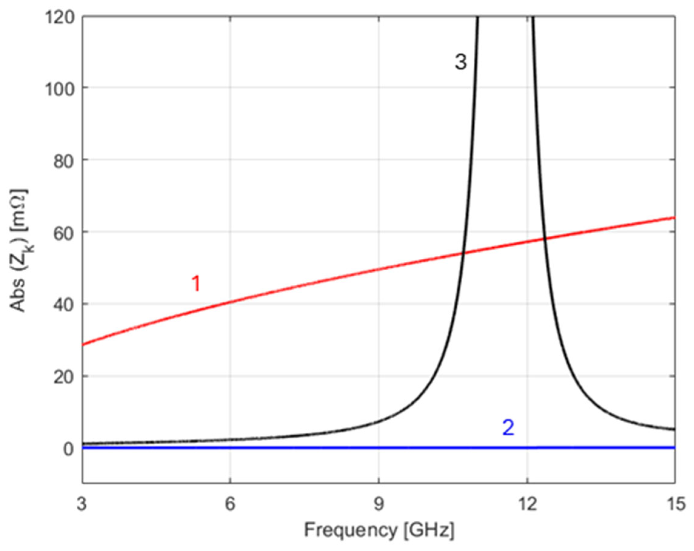
The abovementioned results for the impedance corrections, due to skin effect phenomena in the capacitor’s imperfect plates (supporting surface currents), are graphically represented in
Figure 10.
For illustration purposes, we assume that both plates, made of aluminum, are 25 μm thick (w = h/20), and with regard to the radius of the lead wires, we used rw = w/5 = 5 μm. The frequency window of the analysis is 3–15 GHz, including the resonance frequencies f1 and f2. It should be emphasized that for this range of frequencies, the field penetration depth (δ in (56)) is of the order of 1 μm, and therefore, the plates with 25 μm of thickness can be considered thick plates.
The graphical plots in
Figure 10 show that the impedance contribution
Z2 (curve 2), proportional to
w/
ro, associated with the plate axial surface currents at
r =
ro, is negligible for
as in [
8]. In fact, for 15 GHz, we found that |Z
2|= 46 μΩ.
The contribution Z1 (curve 1), proportional to ln(ro/rw), associated with the radial surface currents at the outer face of the plate (z = 0), is critically dependent on the radius of the lead wire bonded to the plate. It is the dominant contribution for frequencies below the resonance frequency f2.
The contribution
Z3 (curve 3), associated with the radial surface currents at the inner face of the plate at
z =
w, is extraordinarily large for frequencies close to
f2 and theoretically infinite if the dielectric were lossless—an aspect disregarded in [
8].
4.4. Lossy Dielectric and Lossy Plates (ID-IC)
The results in the previous section, which concern the contribution of the imperfect plates to the device impedance, were obtained by considering that the dielectric core of the device was a perfect dielectric (PD). Now, we remove this assumption, considering that the permittivity is complex, as in (52), and consequently, that
κ and
ρ become complex numbers. Now, we aim to find
as follows:
where
is obtained from (51).
We need not worry about alterations to the impedance contributions , in (60), because they do not depend on the dielectric medium; only does.
We may reuse (63) to calculate
, but with some caution. Replacing
κ with
(and
ρ with
is essential but will not suffice; we also need to replace the squared real Bessel functions with the absolute value of the squared complex Bessel functions, as follows:
The calculation of the integral on the right-hand side of (68) is addressed in
Appendix A and leads to the following simple result:
The result in (69) can be particularized for the case of
ρ << 1 (via series expansions) and for the case of
ρ >> 1 (via asymptotic expansions), yielding:
Using (69), the plate contribution in (67) to the device impedance becomes
Finally, by simultaneously considering the dielectric and plate imperfections, the device impedance is obtained from:
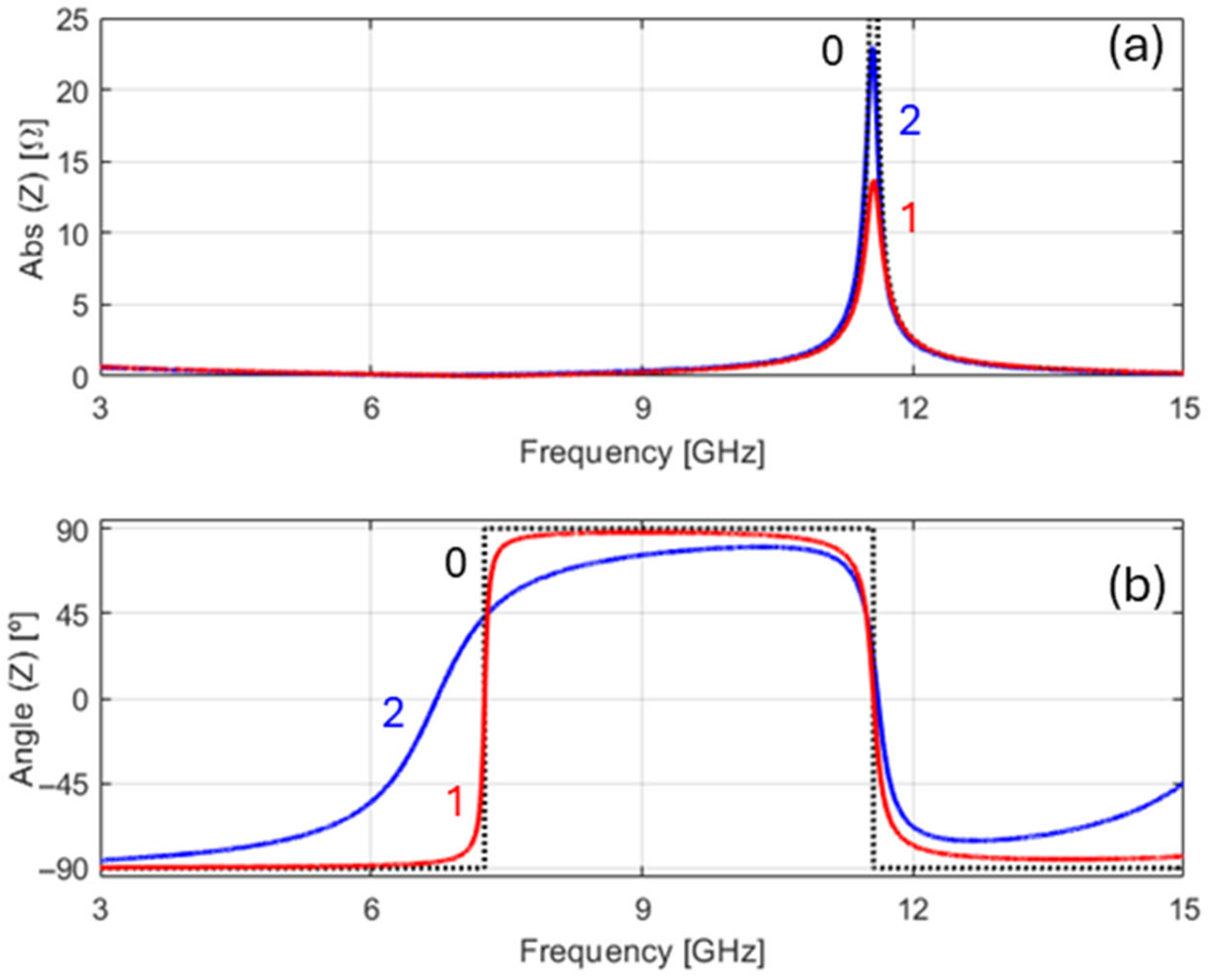
Graphical results for the modulus and angle of the device’s impedance in (72) against the frequency, for the full lossy case, are shown in
Figure 11 (curves 2 in blue).
For comparison purposes, we also repeated the impedance plots for the other addressed cases, the ID/PC case (curves 1), and the PD/PC case (curves 0) in
Figure 11. The results in
Figure 11 show that the impedance peak at
f =
f2 has almost doubled from 14 Ω to about 23 Ω, owing to conductor imperfection. The most important mechanism responsible for this increase is the presence of radial currents on the inner faces of the capacitor plates.
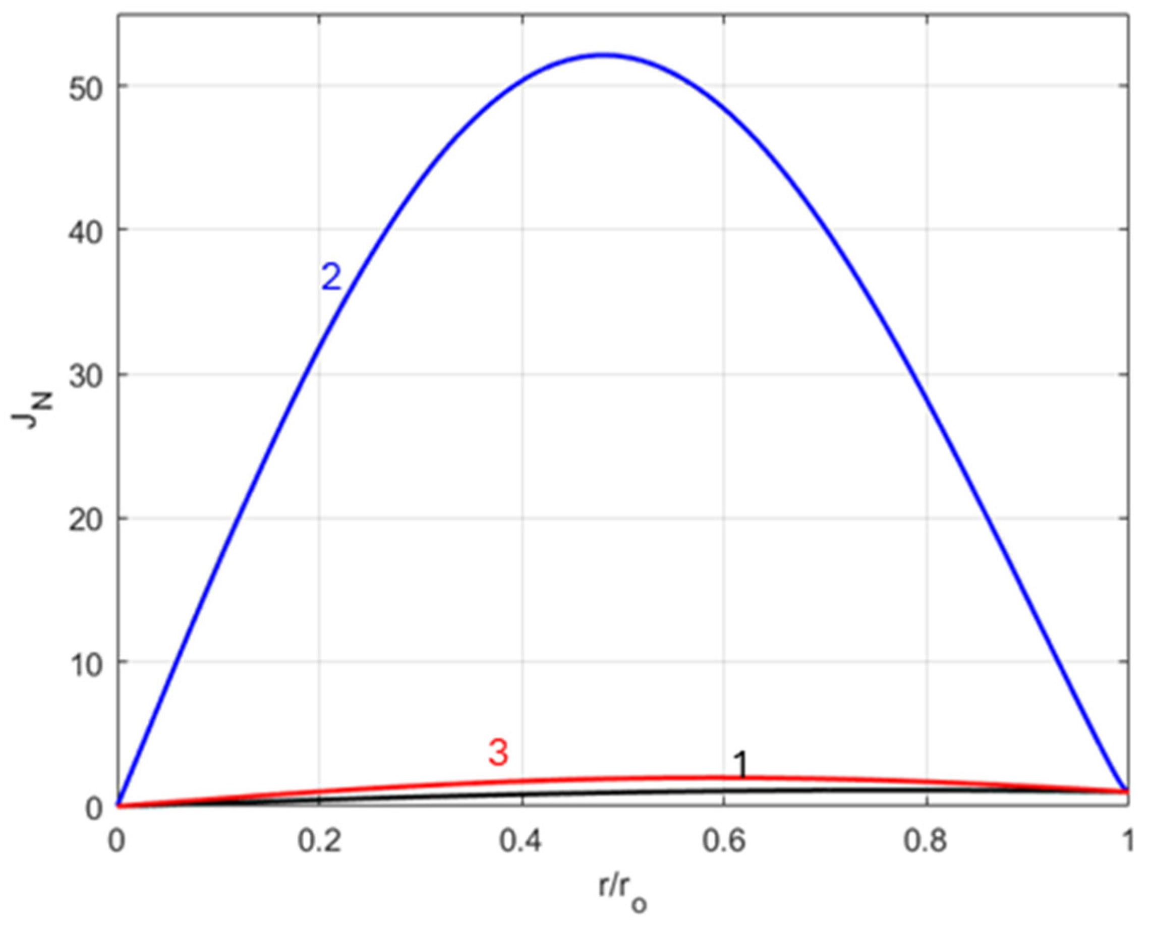
The density of the radial surface currents
JS(
r) on the inner faces of the plates (surface S
3 in
Figure 9) was evaluated in (55) for the lossless dielectric case. The result in (55) can be easily generalized for the lossy case by substituting the real wavenumber
, with its complex version
, where the complex permittivity has already been defined in (52); then, for the ID/IC case, the radial surface current is given by:
and its rms value is defined as follows:
where the real function
JN(
r) represents the normalized surface current density, which is equal to 0 when
r = 0 and equal to 1 when
r =
ro.
We computed and plotted the function
JN against
r/
ro for three different frequencies: the resonance frequencies
f1 and
f2, and one in the middle
f3 = (
f1 +
f2)/2. The results presented in
Figure 12 clearly show that the surface current at
f =
f2 (blue curve) crowds near the circumference of radius
r =
ro/2, and that its intensity largely exceeds those of the other currents. If dielectric losses were much lower than those considered in the simulation (loss angle
mrad), then the maximum of
JN would increase to well over 50.
Table 2 provides a set of computed numerical values for the device’s complex impedance (inductive behavior) for the frequencies
f1,
f2, and (
f1 +
f2)/2, which are considered in the graph plots in
Figure 12.


