Article

Enhanced Charge Transport in Inverted Perovskite Solar Cells via Electrodeposited La-Modified NiOx Layers

by
Lina Aristizábal-Duarte
1,
Martín González-Hernández
1,
Sergio E. Reyes
2,
J. A. Ramírez-Rincón
3,
Pablo Ortiz
2 and
María T. Cortés
1,*
1
Department of Chemistry, Universidad de los Andes, Bogotá 111711, Colombia
2
Department of Chemical Engineering, Universidad de los Andes, Bogotá 111711, Colombia
3
Grupo de Investigación en Ciencias y Educación, Facultad de Ingeniería, Universidad de América, Bogotá 111211, Colombia
*
Author to whom correspondence should be addressed.
Energies 2025, 18(14), 3590; https://doi.org/10.3390/en18143590
Submission received: 20 May 2025 / Revised: 25 June 2025 / Accepted: 3 July 2025 / Published: 8 July 2025
(This article belongs to the Section A2: Solar Energy and Photovoltaic Systems)

Abstract

This work explored an electrochemical approach for synthesizing lanthanum-modified nickel oxide (NiOx:La) as a hole transport layer (HTL) in inverted perovskite solar cells (IPSCs). By varying the La3+ concentration, the chemical, charge transport, structural, and morphological properties of the NiOx:La film and the HTL/PVK interface were evaluated to enhance photovoltaic performance. X-ray photoelectron spectroscopy (XPS) confirmed La3+ incorporation, a higher Ni3+/Ni3+ ratio, and a valence band shift, improving p-type conductivity. Electrochemical impedance spectroscopy and Mott–Schottky analyses indicated that NiOx:La 0.5% exhibited the lowest resistance and the highest carrier density, correlating with higher recombination resistance. The NiOx:La 0.5% based cell achieved a PCE of 20.08%. XRD and SEM confirmed no significant changes in PVK structure, while photoluminescence extinction demonstrated improved charge extraction. After 50 days, this cell retained 80% of its initial PCE, whereas a pristine NiOx device retained 75%. Hyperspectral imaging revealed lower optical absorption loss and better homogeneity. These results highlight NiOx:La as a promising HTL for efficient and stable IPSCs.

1. Introduction

Among the solar energy technologies currently under development, perovskite solar cells (PSCs) have gained prominence over the past decade due to their moderate production costs, increasing efficiencies, and compatibility with flexible substrates. Advances in fabrication processes and material properties have steadily improved power conversion efficiency (PCE), from 3.8%, first reported by Miyasaka et al. in 2009 [1], to a recent 26.1% in 2024 [2].
Despite these advances, PSCs still face critical challenges that require further laboratory-scale research. The main obstacles include long-term stability, the toxicity of lead-based perovskites, and scalability for commercial production [3,4]. Among the various materials in a PSC, the hole transport layer (HTL) plays a crucial role in charge extraction, transport, and interfacial stability, directly influencing the device’s performance parameters [5].
Optimal HTL performance strongly depends on the alignment of energy levels, conductivity, and film quality. Proper alignment of energy levels at the interface with the perovskite (PVK) promotes efficient charge extraction and separation. High conductivity in the HTL minimizes recombination and facilitates charge transport, improving the cell’s fill factor [6]. Additionally, the surface quality of the HTL enhances interfacial contact with the PVK and prevents charge drift.
The position of the HTL varies depending on the configuration of the PSC. In n-i-p structured cells, light first passes through the electron transport layer (ETL) before reaching the PVK. In contrast, in inverted p-i-n cells, the HTL is deposited before the PVK, reversing the layer sequence compared to the conventional structure. In particular, inverted perovskite solar cells (IPSCs) are of great interest due to their higher processability and simpler assembly, which is especially advantageous for flexible substrate devices [4,7].
Two-dimensional (2D) materials have recently complemented conventional transport layers in PSCs. Graphene-based ETL composites can push simulated efficiencies beyond 26% and improve moisture tolerance [8], while MXene Ti3C2Tx interlayers tune the work function and lift single-junction PCEs above 22% [9]. Although effective, these 2D modifiers often require vacuum or acid-etch processing. Because of these processing drawbacks, researchers continue to seek scalable alternatives, most notably solution-processable semiconducting oxides. These compounds possess the desirable characteristics of hole-transporting materials while also offering significant advantages, such as good chemical and thermal stability, low hygroscopicity, and low cost, making them a promising alternative to organic HTLs like spiro-OMeTAD, PEDOT:PSS, and P3HT [10]. Among them, nickel oxide (NiOx) stands out for its high charge carrier mobility, fast charge injection, and relatively wide bandgap (Eg > 3.5 eV). NiOx is particularly used in inverted photovoltaic devices due to its requirement for high annealing temperatures (around 300 °C) [11].
Although NiOx exhibits acceptable charge transport and stability properties, these characteristics can be further enhanced through various strategies, such as solvent engineering to improve ohmic contact, layer structuring methods to promote nanostructuring, post-treatments to reduce defects, and material doping. In particular, metal oxide doping has proven to be an effective approach for enhancing hole transport properties by increasing conductivity, improving charge extraction, enabling surface passivation, and optimizing work function alignment. Studies have shown that doping NiOx with metals such as K+, Ag+, Cu2+, Co2+, and In3+ can enhance both the efficiency and stability of PSCs [12]. A particularly interesting approach involves doping NiOx with rare earth elements, which can further refine its charge transport and interfacial properties. In this context, Chen et al. studied the doping of NiOx with rare earth elements such as Ce, Nd, Eu, Tb, and Yb using a solution-based method, observing improvements in surface passivation and band alignment at the NiOx heterojunctions. The best results were obtained with 3% Eu, which increased the PCE from 12.20% to 15.06%, attributed to more efficient charge extraction and reduced interfacial recombination. They reported a 30% increase in PVK grain size compared to undoped NiOx, an improvement attributed to reduced defect density, while the initial cell efficiency retained 97% of its value after 10 days [13]. Similarly, Hu et al. doped NiOx with 5% yttrium via a sol-gel route and achieved 16.3% efficiency, attributing the improvement to higher hole mobility and reduced recombination [14]. Teo S et al. first explored La-modified NiOx prepared from LaCl3 via a solution route and showed that 3% La raised IPSC efficiency to 15.46% by enlarging perovskite grains, improving film quality, and enhancing charge transport/extraction. The devices retained 95% of their initial efficiency after 50 days [15]. Most recently, Chappidi et al. prepared La:NiOx by spray pyrolysis, achieving 22.4% and attributing the gain to suppressed interfacial defect density [16]. These studies generally rely on high La loadings (≥3%) and organic solvents or high-temperature pyrolysis.
Here, we demonstrate for the first time aqueous electro-deposition of ultra-low-content La-modified NiOx (0.5 mol%) as an HTL for inverted PSCs. The method affords precise control over film thickness and uniformity while avoiding toxic organic solvents by using an aqueous electrolyte [17]. Introducing only 0.5% La3+ in the electrosynthesis solution produced NiOx:La films that markedly improved device performance: charge carrier density increased, HTL resistance decreased, and charge extraction from the PVK was enhanced, as confirmed by EIS, IS, PL, and Mott–Schottky analyses. These changes delivered a maximum PCE of 20.06%, among the top values obtained with La loading of less than 1% in IPSCs. XPS confirmed La incorporation, and SEM showed that the optimal La concentration in NiOx does not significantly alter the PVK grain size.
The champion cell retained 80% of its initial efficiency after 50 days, and hyperspectral imaging, applied here for the first time, revealed improved optical homogeneity at the PVK/HTL interface under the optimal La concentration. Together, these results establish a route to high-performance La-modified NiOx HTLs and provide new insights into how rare-earth additives govern interfacial optoelectronic behavior.

2. Materials and Methods

2.1. Electrochemical Synthesis of La-Modified NiOx Layers

NiOx electrodeposition was carried out in a three-electrode electrochemical cell using an ITO-coated glass substrate (submerged area: 1 cm3) as the working electrode, a platinum wire as the counter electrode, and Ag/AgCl (3 M NaCl) as the reference electrode. Prior to deposition, the ITO substrates were carefully cleaned by gentle scrubbing with a soft brush using ultrapure water and neutral soap. Subsequently, the substrates were immersed in a soap solution and sonicated for 15 min. Afterwards, they were thoroughly rinsed with deionized water and subjected to two additional ultrasonic cleaning cycles in fresh deionized water, each lasting 15 min. Finally, the substrates were dried with compressed air and placed in an oven at 90 °C for 20 min.
The synthesis solution was prepared using 0.01 M NiCl2 (99.9985%, Merck, Darmstadt, Germany) in 50 mM NaNO3 at pH ≈ 5, along with LaCl3·7H2O (98%, Merck, Darmstadt, Germany). The mass of LaCl3·7H2O was adjusted to obtain La:Ni mole fraction solutions of 0.5%, 1%, and 2%, which were used for the electrodeposition of La-modified NiOx layers (NiOx:La 0.5%, NiOx:La 1%, and NiOx:La 2%). Because XPS shows that La does not occupy substitutional or interstitial lattice sites (see Section 3.1), we refer to these films as La-modified NiOx. Additionally, a lanthanum-free solution was also prepared for the deposition unmodified NiOx. The electrodeposition (ECD) was performed via galvanostatic chronopotentiometry using a potentiostat (Autolab PGSTAT302N, Metrohm Autolab B.V., Utrecht, The Netherlands). A sequence of ten current pulses was applied from 0 V to ~−0.9 V, each consisting of an on-time (ton) of 25 s and a relaxation time (toff) of 2 s at open circuit. The current was adjusted to deliver a total charge of 0.5 mC cm3 per pulse. After deposition, the films were rinsed with deionized water, dried in air, and annealed at 300 °C for 1.5 h on a ceramic plate to obtain NiOx and La-modified NiOx layers.

2.2. Inverted Perovskite Solar Cell Fabrication

The solar cells were fabricated inside a glovebox with a constant flow of N2 and a relative humidity of 26%. The perovskite solution (PVK) (CH3NH3PbI3) was prepared using 1.2 mmol of methylammonium iodide (MAI) and 1.2 mmol of lead iodide in 1 mL of a DMF: DMSO mixture (10:1 v/v). For the [6.6] phenyl-C61-butyric acid methyl ester (PCBM) layer, a 20 mg/mL solution was prepared in 1 mL of chlorobenzene. Finally, a 0.5 mg/mL solution of bathocuproine (BCP) in a methanol:toluene (100:1 v/v) solution was prepared.
For the coatings of the IPSC heterojunctions, 30 μL of the PVK solution was deposited onto the NiOx/ITO substrate by spin-coating at 1000 rpm for 10 s, followed by 5000 rpm for 15 s. After 18 s, 350 μL of chlorobenzene was quickly added. Subsequently, the PCBM layer was applied by spin-coating 30 μL of the solution at 5000 rpm for 30 s, followed by annealing at 100 °C for 30 min. Finally, 40 μL of BCP was spin-coated at 4000 rpm for 40 s. To form the metallic contacts, thermal evaporation of Ag was performed at a deposition rate of 0.1 Å s−1 until and about a thickness of 130 nm was achieved. In this way, ITO/NiOx/PVK/PCBM/Ag solar cells were fabricated.

2.3. Characterization Methods

2.3.1. Electrochemical Characterization of La-Modified NiOx

The charge transport properties of the HTLs were evaluated by electrochemical impedance spectroscopy (EIS) in a 5 mM Fe (CN)63−/4− solution in 0.1 M KCl at a potential of 0.4 V DC versus Ag/AgCl. The frequency was varied from 100 kHz to 0.1 Hz with an AC perturbation amplitude of 10 mV. Mott–Schottky data were obtained by applying a 10 mV AC perturbation at 1000 Hz, with each DC potential point held for 10 s before measurement.
Characterization by cyclic voltammetry (CV) was performed to determine the HOMO level over a potential range of 0 to 1.0 V in 0.1 M KCl, using 0.5 mM K3Fe(CN)6 as the reference system and a potential window from −0.2 to 1.0 V. A three-electrode system was employed, consisting of Ag/AgCl as the reference electrode (RE), platinum as the counter electrode (CE), and ITO/NiOx as the working electrode (WE), with a scan rate of 100 mV s−1.

2.3.2. Physicochemical Characterization of La-Modified NiOx

The optical properties of the HTL were characterized by UV–vis absorption spectra with a Thermo Scientific Genesys 10S spectrophotometer (Thermo Scientific, Waltham, MA, USA). Photoluminescence (PL) measurements were conducted on a Cary Eclipse fluorescence spectrophotometer (Agilent Technologies, Santa Clara, CA, USA) with an excitation wavelength of 405 nm. X-ray diffraction (XRD) patterns were obtained using a Rigaku Ultima III instrument (Rigaku Corporation, Tokyo, Japan) with CuKα radiation (λ = 0.15406 nm) over a 2θ range of 10° to 70° and with a step size of 0.02° and a beam exposure of 3 s per step. Scanning electron microscopy (SEM) was used to evaluate the PVK morphology and the cross section of the entire solar cell with a Tescan Lyra 3 microscope. SEM/EDS analysis of thicker NiOx:La films (~120 nm) was performed to assess La incorporation, using an accelerating voltage of 8.0 kV and 60,000× magnification.
The optical absorption loss of the PVK layer was monitored with a SPECIM IQ hyperspectral camera (204 bands, 400–1000 nm; ≈256 000 spectra per image) (SPECS, Berlin, Germany) and processed in ENVI 5.3. Unencapsulated ITO/HTL/PVK samples were stored in the dark at room temperature (20 ± 2 °C) and ambient air (no control of O2, H2O, or humidity) for 50 days; hyperspectral images were acquired every 10 days. Darkness was the only rigorously maintained condition, allowing us to isolate intrinsic changes in the perovskite/HTL stack.
XPS measurements of the HTL were conducted using the XPS/ISS/UPS surface characterization platform A. Centeno, built by SPECS (Germany). The platform featured a 2-CMOS 150 energy analyzer. Experiments were performed with a monochromatic Al Kα X-ray source (FOCUS 500) operated at 100 W. The pass energy of the hemispherical analyzer was set to 100 eV for survey spectra and 20 eV for high-resolution spectra. Surface charge compensation was controlled using a Flood Gun (FG 15/40-PS FG 500, SPECS GmbH, Berlin, Germany), operated at 20 μA and −0.8 eV. The analyzed regions included C1s, O1s, Ni2p, La3d, Cl2p, Sn3d, In3d, Cl2p, and the valence band (VB). At the end of each analysis, the C1s region was remeasured to monitor surface charging evolution during the experiment.

2.3.3. Photovoltaic Characterization of Inverted Perovskite Solar Cells (IPSC)

J-V curves of the IPSCs were measured under simulated AM 1.5G sunlight (100 mW cm−2) using an Abet Technologies model 10,500 simulator (Abet Technologies, Inc., Milford, CT, USA). A potential sweep was applied from −0.1 to 1.1 V at 50 mV s−1 using an Autolab AUT84194 potentiostat (Autolab PGSTAT302N, Metrohm Autolab B.V., Utrecht, The Netherlands). The light intensity was calibrated using a Hamamatsu S1133 photodiode (Hamamatsu Photonics K.K., Hamamatsu, Japan), and the illuminated area of the cells was restricted to 0.065 cm2 using a black mask. Parameters such as power conversion efficiency (PCE), short-circuit current density (Jsc), open-circuit voltage (Voc), fill factor (FF), series resistance (Rs), and shunt resistance (Rsh) were determined from J-V curves. Steady-state PCE measurements were conducted at 0.75 V during 3000 s, while impedance spectroscopy (IS) was performed under inert atmosphere conditions (N2) at 0.1 V across a frequency range of 0.1 Hz to 1 MHz under illumination from the solar simulator. The stability of the solar cells was evaluated from day 0 to day 50 by measuring J-V curves under standard AM 1.5 G illumination (100 mW cm3). Unencapsulated devices were stored at room temperature (20 ± 2 °C) in the dark under a nitrogen atmosphere; each sample was sealed in a Ziploc bag with silica-gel desiccant to minimize exposure to moisture and oxygen.

3. Results and Discussions

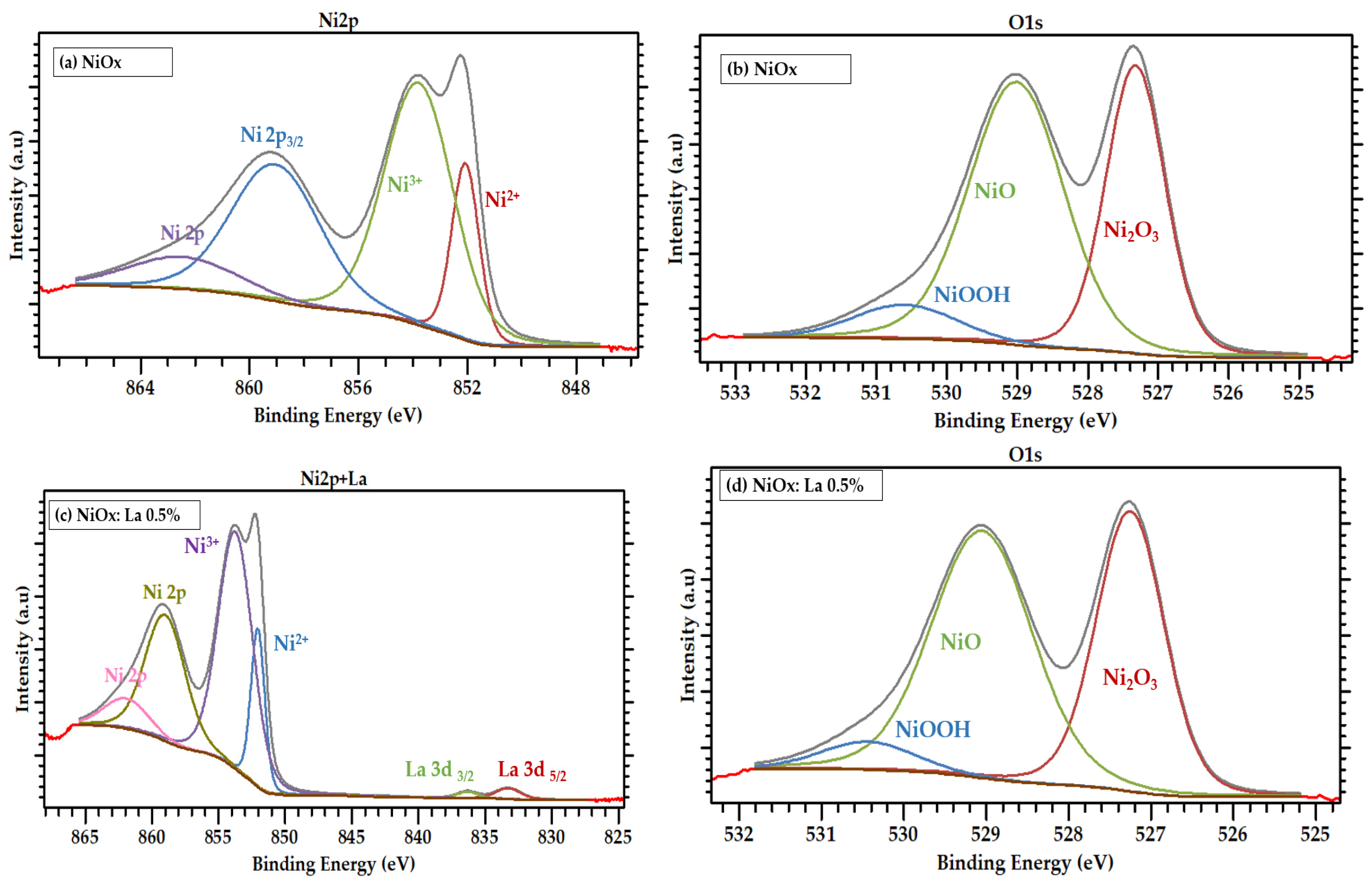
3.1. Electrochemical Synthesis and Chemical Characterization of La-Modified NiOx

During the electrochemical deposition (ECD) of nickel hydroxide (Ni(OH)2) on an ITO substrate, the application of a cathodic pulsed current leads to the reduction of nitrate ions (NO3) to nitrite (NO2), simultaneously releasing hydroxyl ions (OH) (Equation (1)), which react with Ni2+ ions present at the interface to form Ni(OH)2 (Equation (2)). A homogeneous layer precipitates on the substrate when the concentration of OH approaches the solubility product of Ni(OH)2, resulting in the formation of its polymorphic structure [18]. Once the ECD process is completed, the coated substrate undergoes thermal treatment at 300 °C, during which Ni(OH)2 decomposes to NiO while releasing water vapor [17] (Equation (3)). Further oxidation of Ni2+ to Ni3+ in an oxygen-rich environment results in the formation of NiOx, a process that generates nickel vacancies due to the induced charge imbalance, which is crucial for enhancing the semiconducting properties of the material [18,19] (Equation (4)). Figure S1 shows the NiOx films electrodeposited on ITO substrates.
N O 3 + H 2 O + 2 e N O 2 + 2 O H
N i 2 + + 2 O H N i ( O H ) 2
N i ( O H ) 2 N i O + H 2 O
2 N i 2 + + 1 2 O 2 O 2 + V N i + 2 N i 3 +
To assess the presence of mixed valence states of nickel and evaluate the effectiveness of the ECD method for lanthanum incorporation, X-ray photoelectron spectroscopy (XPS) was performed on NiOx and NiOx:La 0.5% layers. Figure S2 shows the obtained XPS spectra over an energy range of 0 to 1200 eV, where characteristic signals for Ni 2p3/2, O 1s, La 3d5/2, and La 3d3/2 were detected with binding energies of approximately ~855, ~527, ~833, and ~836 eV, respectively. Due to the thin nature of the HTL layer (~30 nm), signals from the ITO substrate, specifically for In 3p3/2 and In 3d5/2, were also observable. The spectra were deconvoluted at different binding energies to confirm the presence of each element and determine their oxidation states. Figure 1 provides high-resolution XPS spectra for NiOx and NiOx:La 0.5%.
The XPS results revealed three main binding energy ranges: 850–865 eV for the Ni 2p3/2 Ni 2p1/2 peaks, 526–532 eV for the O 1s peak, and 830–840 eV for the La 3d3/2 and La 3d5/2 peaks. Figure 1a,c show the Ni 2p3/2 peaks for NiOx and NiOx:La 0.5%. For NiOx, the main peaks appear at 852 eV (Ni2+) and 853.6 eV (Ni3+), while for NiOx:La 0.5%, they appear at 852.1 eV (Ni2+) and 853.7 eV (Ni3+) [15,20,21]. In each case, the gray curve corresponds to the non-deconvoluted total spectra (Figure 1). The doublet associated with the mixed oxidation states of nickel (Ni3+/Ni2+) is commonly attributed to nickel vacancies or the formation of holes within the NiOx lattice [22]. The inclusion of La3+ led to an increase in the Ni3+/Ni2+ ratio from 1.69 in NiOx to 2.81 in NiOx:La 0.5%, indicating enhanced p-type conductivity due to modification [23,24].
Figure 1c displays signals corresponding to the 3d3/2 and 3d5/2 states of La3+, observed at binding energies of 836.4 eV and 833.1 eV, respectively, confirming its incorporation in NiOx [25]. Deconvolution of the O 1s peak (Figure 1b,d) revealed characteristic contributions from NiO, Ni2O3, and NiOOH, with binding energies at 529.0 eV, 527.2 eV, and 530.4 eV, respectively [26]. According to the elemental composition data (Table S1), the presence of La was confirmed, alongside Ni and Cl species derived from the precursor solutions. Additionally, signals corresponding to In and Sn, characteristic of the ITO substrate, were also detected.
Table S2 presents the binding energy (BE) values and full width at half maximum (FWHM) for both oxides. NiOx:La 0.5% exhibits some broader peaks, indicating structural disorder caused by a more heterogeneous chemical environment upon La3+ incorporation, which in turn alters the electronic structure and expands the binding energy (BE) range [17,25,26].
Regarding the nature of La incorporation in NiOx, the invariance of the Ni 2p3/2 and O 1s binding energies rules out substitutional La3+/Ni2+ exchange, because even trace substitution is known to perturb the Madelung potential of neighboring Ni and O ions and produce ≥ 0.2 eV shifts or peak broadening [27]. At the same time, the absence of new shoulders or satellite intensity in Ni 2p and O 1s argues against interstitial incorporation, which for a large cation such as La3+ (115 pm vs. 72 pm for octahedral Ni3+) would be expected to distort the lattice detectably. Instead, the increase in the Ni3+/Ni2+ ratio is consistent with charge compensation via nickel vacancies generated alongside an amorphous, La-rich phase that is intermixed within the oxide film. Surface-sensitive measurements corroborate this picture. If La segregated strongly at the NiOx surface, changes in surface polarity should alter the wetting of the PVK precursor ink; yet, contact angle experiments give virtually identical values for pristine NiOx and La- NiOx (≈30°) (Figure S3), implying that the La does not accumulate at the outermost surface in amounts large enough to modify its chemistry or roughness. Collectively, the XPS and wettability data therefore suggest that La is dispersed throughout the film as a separated, amorphous La-containing phase finely intermixed with NiOx, rather than entering the lattice substitutionally or decorating the surface as a continuous layer. This finding aligns with the work of Teo et al. [15], who propose that La3+ may be incorporated in an amorphous phase and contrasts with systems doped with cations of similar ionic radius to Ni3+ (e.g., Li+ or Mg3+), where substitutional incorporation on Ni sites is the most plausible mechanism [28].
Figures S4 and S5 illustrate the XPS data of the valence band (VB) region and the vicinity of the Fermi level (Ef). Distinct features include the O 2p orbitals contribution (signal A at ~16 eV) and Ni 3p–O 2p hybridized states (signals B at ~1.3 eV and C at 0 eV); peak C may also be attributed to La 5d–O 2p states. Additionally, the NiOx:La 0.5% sample exhibits more intense and better-defined features, suggesting the formation of new electronic states at the Fermi level [29,30]. The shift of Ef relative to the valence band maximum (VBM) was 1.35 eV for NiOx and 1.30 eV for NiOx:La 0.5%, a reduction that has been associated with increased hole concentration and, consequently, enhanced conductivity of the HTL [29,31].

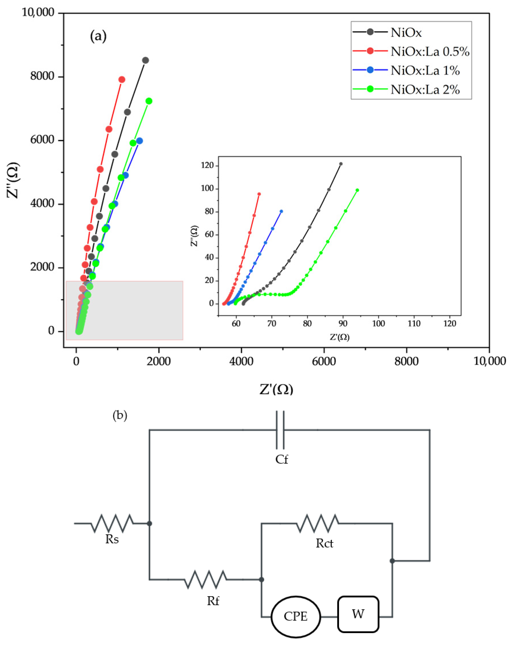
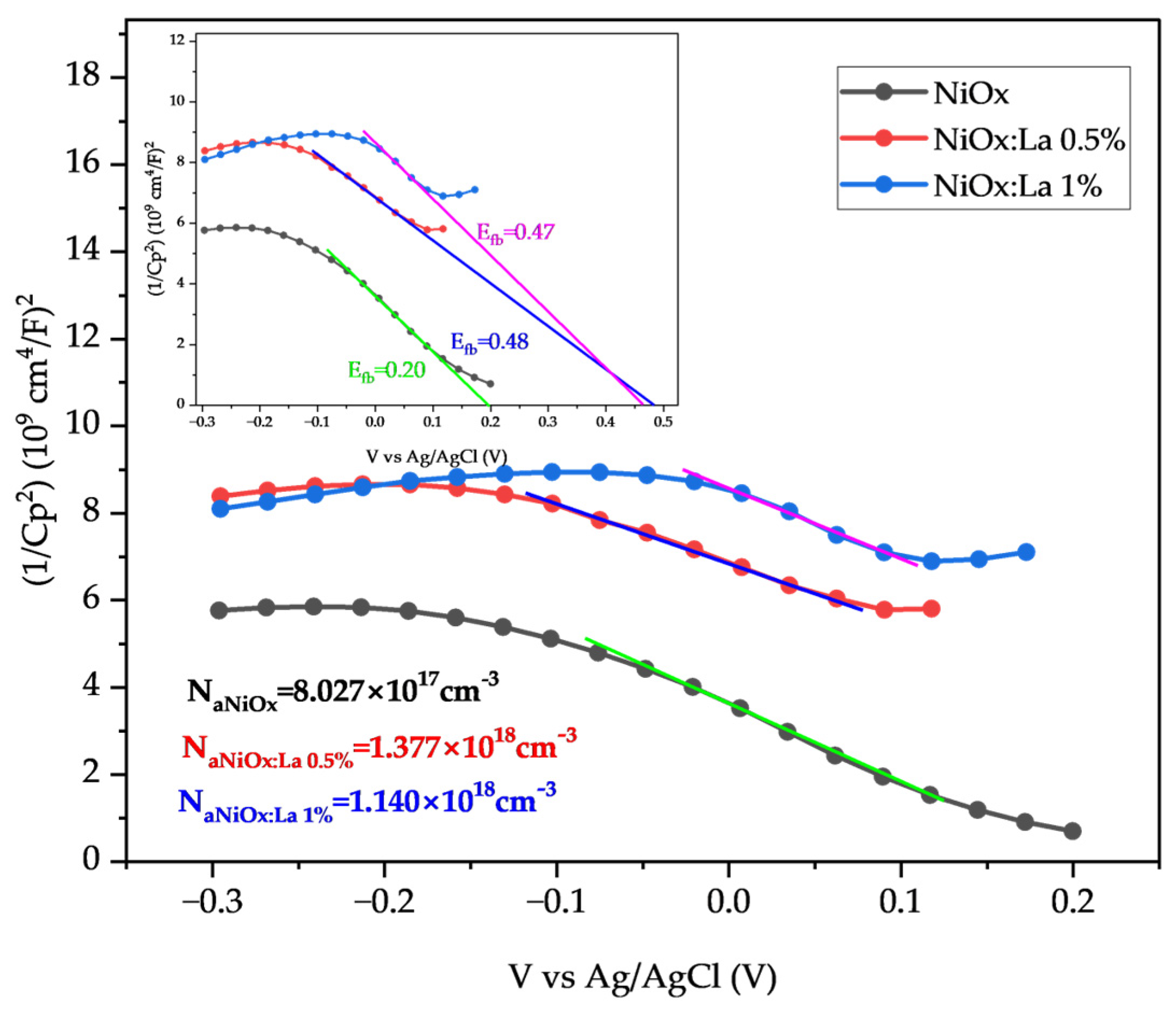
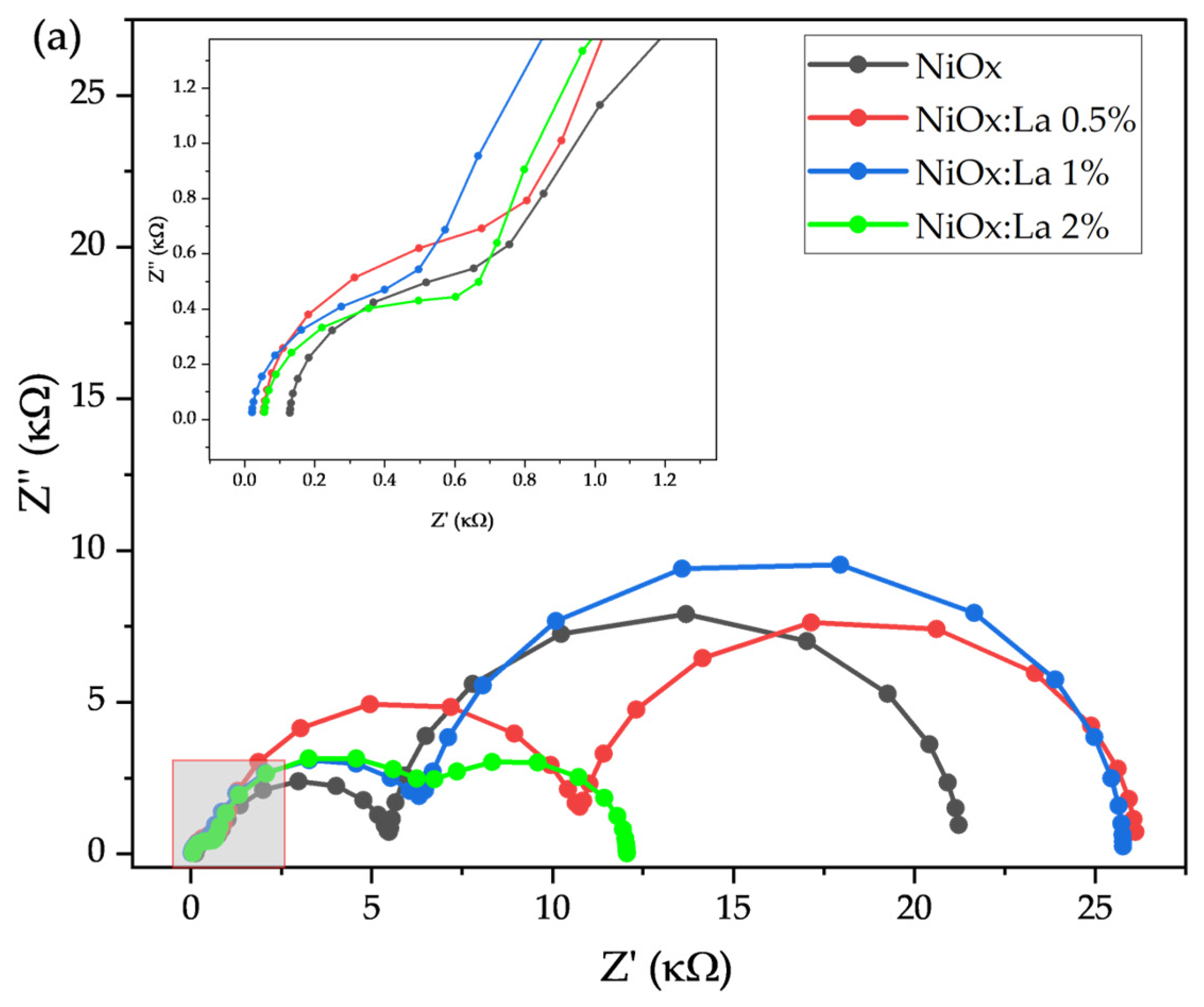
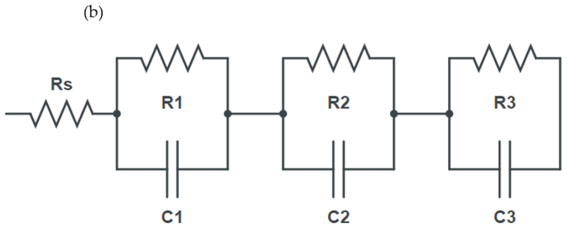
3.2. Electrochemical Characterization of La-Modified NiOx (HTL)

Electrochemical impedance spectroscopy (EIS) measurements were conducted to evaluate the charge transport properties of NiOx HTL’s. Figure 2a presents the Nyquist plots and corresponding equivalent circuit for NiOx, NiOx:La 0.5%, NiOx:La 1%, NiOx:La 2% layers on ITO. The layer resistance (Rf) values varied as follows: NiOx (11.9 Ω), NiOx:La 0.5% (1.14 Ω), NiOx:La 1% (2.66 Ω), and NiOx:La 2% (16.0 Ω). NiOx:La 0.5% exhibited the lowest Rf value, indicating the highest conductivity among the layers. The conductivity improvement is concentration-dependent, as increasing the La3+ content beyond 0.5% leads to a rise in resistance. This trend suggests that La3+ concentrations exceeding 0.5% in solution introduce structural distortions and defects in the oxide, which act as scattering centers for charge carriers [14]. Similar findings have been reported in previous studies, indicating that an optimal concentration exists, beyond which the benefits of modification are lost, and the material becomes more resistive [32,33,34,35].
The equivalent circuit (Figure 2b) consists of a series of resistance (Rs) associated with the electrolyte, an ohmic resistance (Rf) of the electrolyte through the layer; this is essentially the bulk resistance of the NiOx layer itself. Cf is the layer capacitance [36]. Rf is in series with the parallel arrangement consisting of a charge transfer resistance (Rct) which represents the kinetic barrier to the electron-transfer reaction, alongside the Warburg diffusion element (W) and a constant phase element (CPE), both of which limit charge transport due to mass diffusion constraints [14,37,38].
From EIS measurements, a Mott–Schottky plot was generated to evaluate the electronic properties of the semiconductor, specifically to determine the conduction type (n- or p-type), charge carrier density (Na), and flat-band potential (Efb) in NiOx layers. Figure 3 presents the plots of C−2 vs. V, where C represents the capacitance and V is the applied DC potential, for NiOx, NiOx:La 0.5%, and NiOx:La 1%. The negative slope of the linear region confirms the p-type character of the semiconducting oxide, classifying it as a hole transport layer (HTL). The charge carrier density (Na) was determined from the slope, while the flat-band potential (Efb) was obtained from the x-axis intercept, following Equation S1.
The obtained Na values were 8.03 × 1017 cm−3 (NiOx), 1.38 × 1018 cm−3 (NiOx:La 0.5%) and 1.14 × 1018 cm−3 (NiOx:La 1%) (Table S3). These results align with the film resistance (Rf) values discussed previously and suggest that NiOx:La 0.5% represents the La optimal level. Beyond this concentration, carrier density does not increase, likely leading to the formation of structural defects that act as carrier traps. It is possible that in NiOx:La 0.5%, La3+ stabilizes the Ni3+/Ni2+ ratio, increasing the concentration of oxygen vacancies in the oxide [39]. Similar work on Co-modified NiOx has likewise reported Na values on the order of 1018 cm−3 and identified an optimal dopant level [40]. Beyond that optimum, an excessive carrier concentration can distort band alignment at the heterojunction, shrink the space-charge region in the absorber, and ultimately lower key performance metrics such as short-circuit current density (Jsc) and power conversion efficiency (PCE) [41,42,43].
The flat-band potential (Efb) of a semiconductor defines the potential at which there is no depletion layer, meaning there is no net band bending at the interface. It serves as an indicator of the position of the Fermi level relative to the reference electrode and is closely linked to the valence band edge, influencing charge extraction and energy level alignment in the device. A positive shift in Efb indicates a downward shift in the Fermi level, meaning the material has a higher hole concentration (more p-type character). The values obtained from the linear region of the Mott–Schottky plot were 0.20 V (NiOx), 0.48 V (NiOx:La 0.5%), and 0.47 V (NiOx:La 1%) vs. Ag/AgCl. NiOx:La 0.5% shows a significant positive shift in Efb indicating enhanced p-type behavior and improved hole transport properties. The value for NiOx:La 1% suggests that further concentration does not significantly alter the electronic structure.

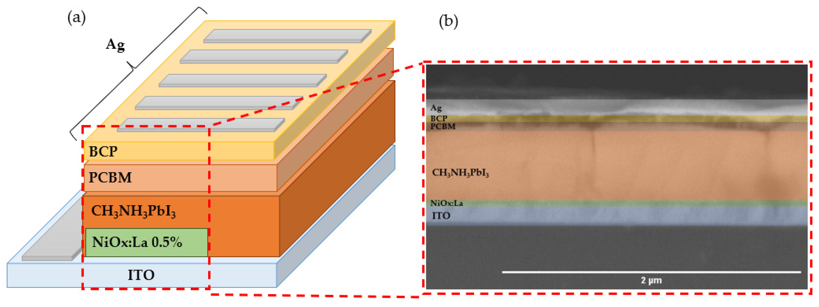
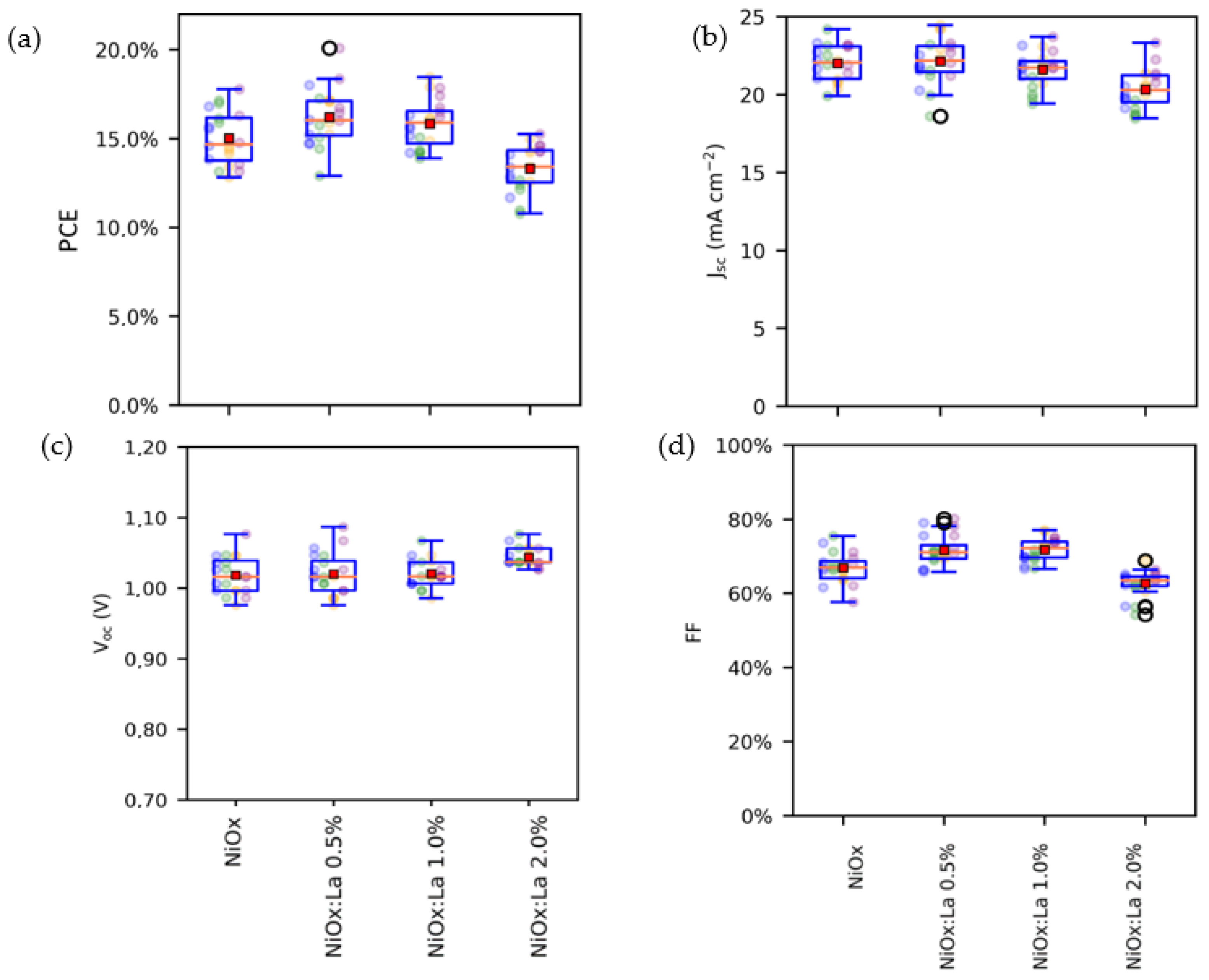
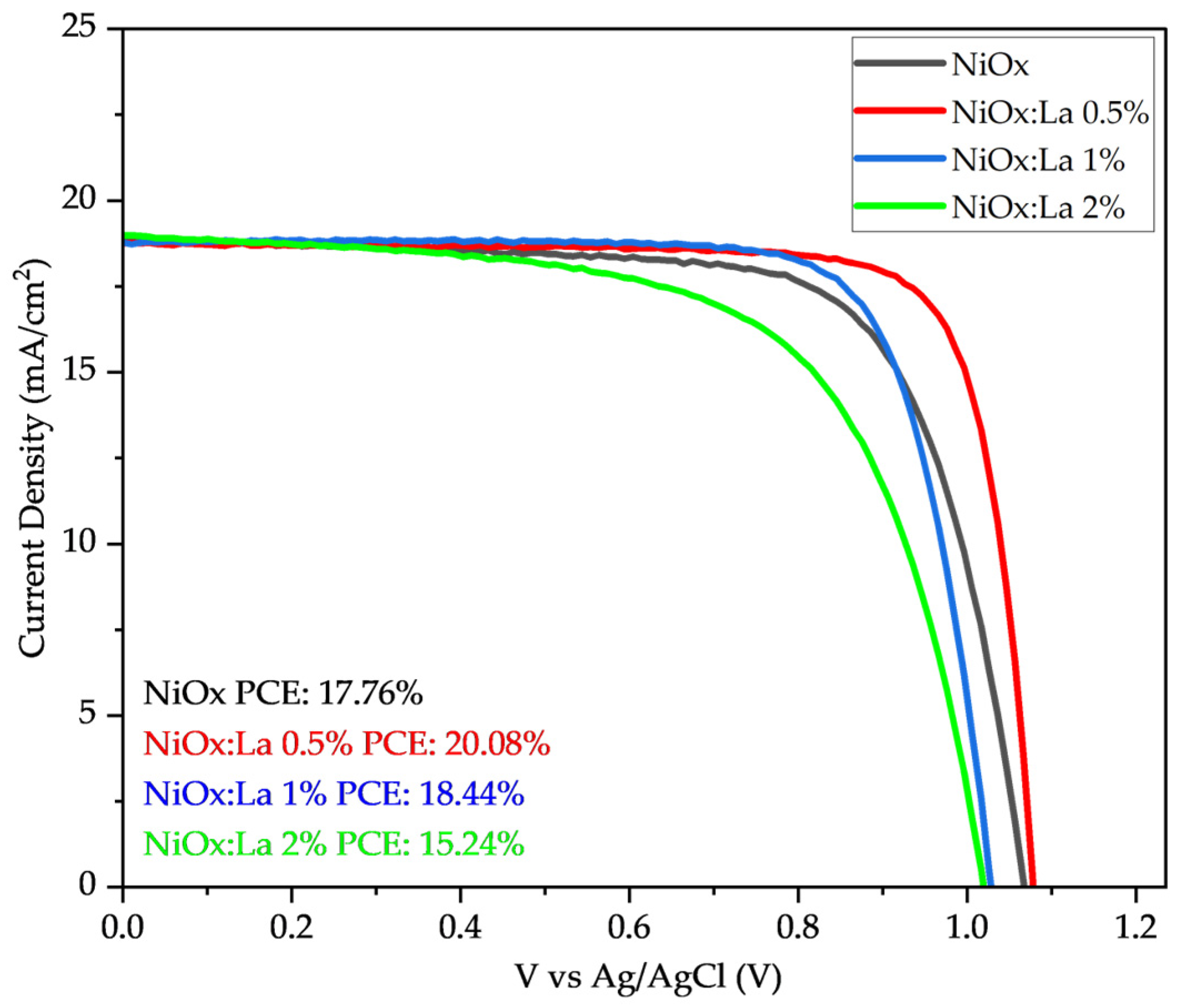
3.3. Photovoltaic Performance of Inverted Perovskite Solar Cells (IPSC)

Inverted perovskite solar cells (IPSCs) with the ITO/NiOx:La/PVK/PCBM/BCP/Ag configuration were fabricated to evaluate the effect of La3+ incorporation in the NiOx layer on the photovoltaic parameters (Figure 4). Prior to these measurements, the cells were characterized in cross section by SEM, confirming the inverted architecture and estimating the thickness of the deposited layers (Figure S6).
The photovoltaic performance was evaluated using J-V curves under simulated AM 1.5G sunlight (100 mW cm−2), with a potential sweep from −0.1 to 1.1 V at 50 mV/s (Figure S7). Table S4 presents the average values and standard deviations of the photovoltaic parameters for the 20 tested devices, and Figure 5 shows the box plots for each photovoltaic parameter in the four cell types. A statistical analysis revealed significant increases in fill factor (FF) with NiOx:La 0.5% compared to pristine NiOx (p < 0.05), contributing to the increased PCE. Specifically, FF improved from 66.90% ± 4.19 (NiOx) to 71.71% ± 4.08 (NiOx:La 0.5%) (Table S4). In contrast, there were no statistically significant variations in PCE between pristine NiOx and NiOx:La 1%. The short-circuit current density (Jsc) and PCE values in the NiOx:La 2% device were statistically lower than those in the NiOx cell.
From Figure 5 and Table S4, it can be observed that the dispersion in photovoltaic parameters was similar across the four HTL types, with approximately 10% for PCE, 5% for Jsc, 6% for FF, and 2% for Voc. These values represent moderate dispersion, which is acceptable for emerging materials and lab-scale cells [44]. The low dispersion in Voc suggests a consistent HTL-PVK interface, indicating good band alignment and PVK stability. In contrast, the moderate dispersion in FF points to some process variability, which could be related to contact resistance or PVK crystallization differences.
The photovoltaic characterization of the cells showed that Jsc and open-circuit voltage (Voc) remained essentially constant across variations (Table S4). This behavior suggests that there are no significant changes in the optical absorption of the PVK layer—as supported by UV–vis and PL measurements—nor were there changes in the bulk or interfacial recombination processes. Consequently, no significant changes in band alignment between the PVK and the HTLs are expected. In contrast, a notable increase in the FF was observed for the NiOx:La 0.5% cell, along with a more squared J-V curve shape, indicating improved HTL/PVK interfacial contact. This improvement is expected to correlate with a lower series resistance (Rs) and a higher shunt resistance (Rsh), as shown in the results below.
Figure 6 presents the J-V curves of the champion devices for each variation. The NiOx:La 0.5% cell achieved the highest PCE at 20.08%, followed by NiOx:La 1% (18.44%), NiOx (17.76%), and NiOx:La 2% (15.24%). The NiOx:La 0.5% cell outperformed the NiOx cell, exhibiting a higher Voc (1.086V) and FF (80.12%) (Table 1).
Series resistance (Rs) and shunt resistance (Rsh) (Figure S8, Table S5) follow the same trend as fill factor (FF) and overall device efficiency. A higher Rs reduces FF by introducing an ohmic voltage drop as current increases, thereby lowering output power. NiOx:La 0.5% exhibits the lowest Rs, indicating superior charge transport and smaller resistive losses, which translate into more efficient current flow [43,44].
Statistical analysis confirmed that Rs for NiOx:La 0.5% is significantly lower than that of pristine NiOx (p = 0.0020). Likewise, a high Rsh reflects minimal current leakage and enhanced operational stability; NiOx:La 0.5% showed the highest Rsh, with a significant difference versus NiOx (p = 0.024). Together, these results demonstrate that optimal La3+ modification of NiOx suppresses charge recombination, reduces leakage, and ultimately boosts photovoltaic efficiency [45,46].
In addition, the performance of the solar cells was evaluated over 3000 s using maximum power point tracking (MPPT) under illumination conditions, with encapsulation in a nitrogen atmosphere at a constant potential of 0.75 V. This approach allowed for monitoring the stability of PCE and Jsc over this period [47].
Figure 7 shows that all four types of solar cells maintained a steady power output, demonstrating stability. This result highlights the effectiveness of the electrodeposition technique and other IPSC production protocols [20]. In all cells, there were slight decreases in Jsc during MPP tracking: 3.49% (NiOx), 1.68% (NiOx:La 1%), 0.93% (NiOx:La 2%), and 0.25% (NiOx:La 0.5%) after 3000 s. As for the PCE values recorded during tracking, they were 15.99%, 15.04%, 14.97% and 17.20%, for the same layers, respectively. This demonstrates a positive effect of La3+ modification, which improves operational stability.
The IPSCs were also characterized using impedance spectroscopy at 0.1 V over a frequency range of 0.1 Hz to 1 MHz under illumination (1 sun). Figure 8a shows the resulting Nyquist plot for each variation, along with the equivalent circuit used to model the data. Determining this equivalent circuit is challenging due to the multilayer nature of the device and the different time scales at which the processes occur, in addition to the effect of ion migration [36]. However, it is common to describe the interfaces present in IPSCs using an equivalent circuit consisting of a series resistance (Rs) connected in series with three parallel RC elements. These correspond to low frequencies (R3, C3), intermediate frequencies (R2, C2), and high frequencies (R1, C1).
Figure 8b illustrates this equivalent circuit, and Table S6 summarizes the fitted values for each circuit element. The resistance R1 characterizes interfacial charge transport, where a lower value is desirable as it corresponds to lower impedance to charge flow. The NiOx:La 0.5% cell exhibited a noticeably larger R1 value, suggesting poorer interfacial conduction in the high-frequency region, possibly due to a less uniform contact between the layers [47].
On the other hand, R2 is associated with intermediate frequencies and represents bulk or interfacial recombination resistance [48,49]. A higher R2 value indicates that charge carriers are less prone to recombination, thereby enhancing cell performance. The fit shows that R2 in the NiOx:La 0.5% cell is significantly higher than in the other cells, increasing by 227% compared to NiOx cell. This suggests that recombination is less likely to occur in the NiOx:La 0.5% cell, contributing to its superior performance.
C1 did not show significant variations across the four cell types, indicating that charge storage in the fast response region remains unchanged with different HTLs. However, NiOx and NiOx:La 0.5% exhibited higher C3 values, which are associated with longer time-scale processes such as ionic migration.
Therefore, according to the IS characterization, the improved photovoltaic performance of the NiOx:La 0.5%-based cell is primarily attributed to its higher recombination resistance, which is consistent with the increased charge carrier density observed in the MS measurements. Despite this advantage, the layer also exhibited higher interfacial charge extraction resistance, which may result from energy level misalignment or interfacial states increasing R1. These results highlight the need for further strategies to improve interfacial contact, such as passivating molecules or interlayers to reduce R1.

3.4. Physical, Morphological, and Optoelectronic Characterization of PVK/HTL

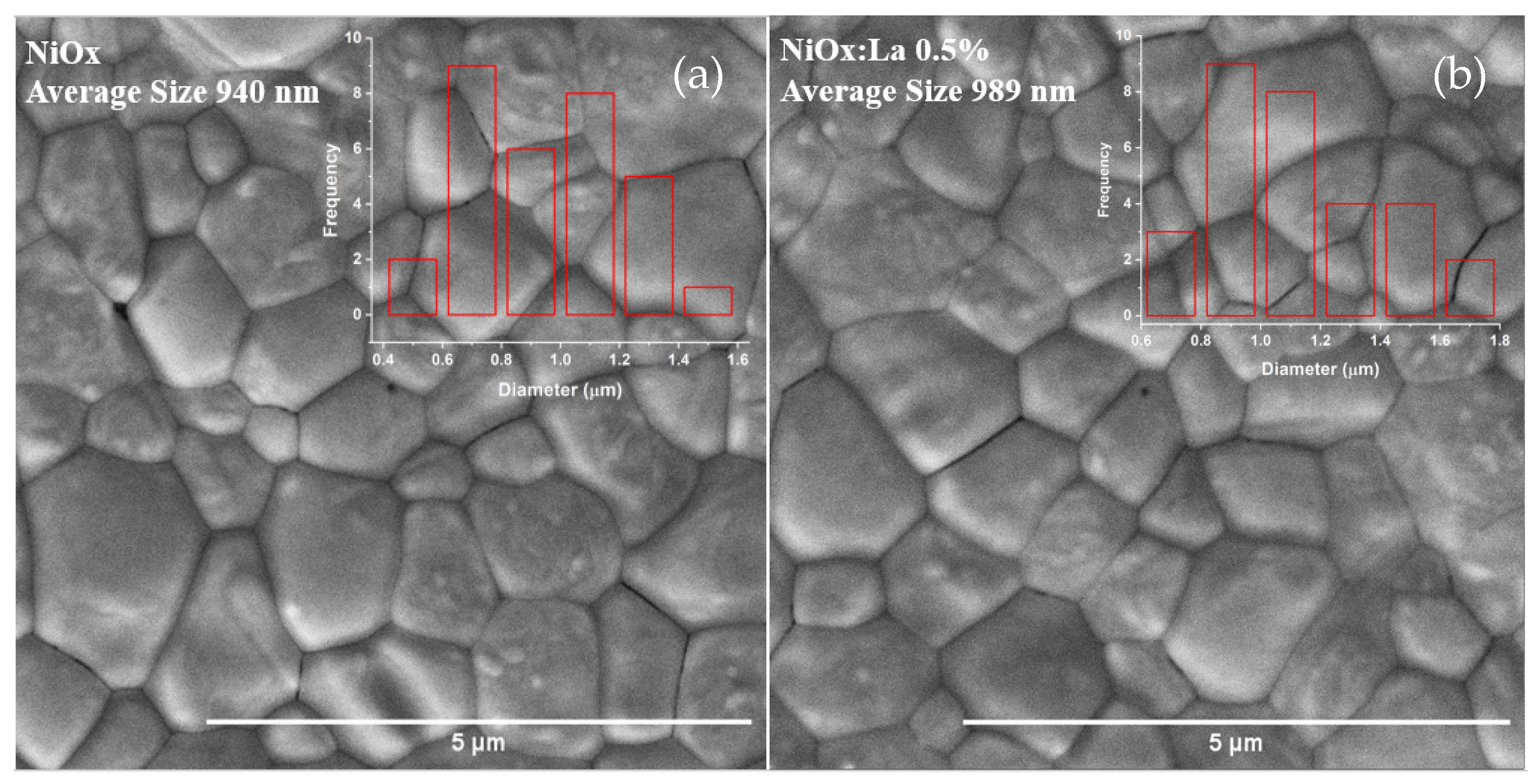
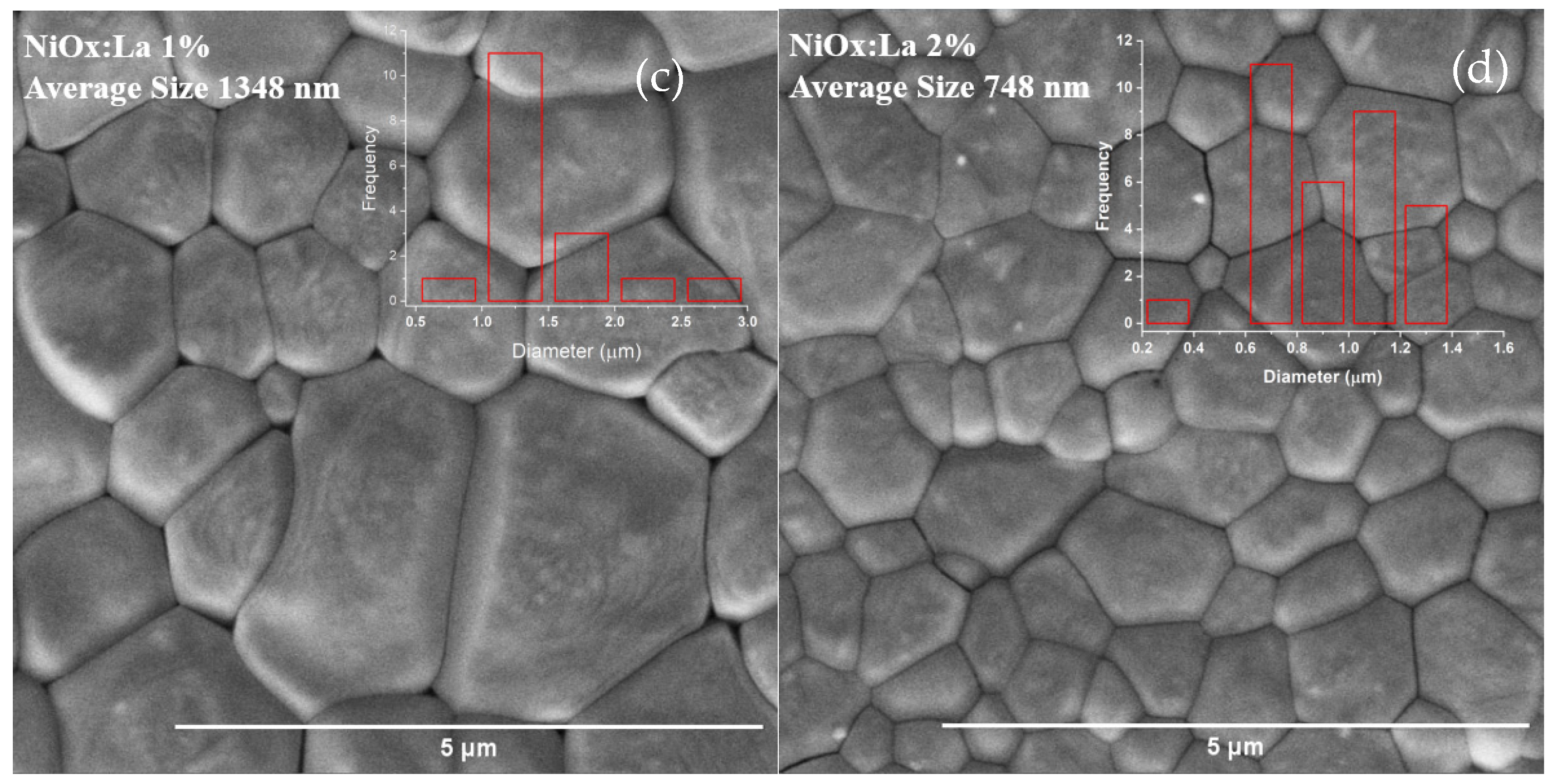
3.4.1. SEM Characterization

The morphology of the PVK layers deposited on each HTL variation was analyzed by SEM to evaluate the influence of La3+ incorporation in NiOx. In inverted devices, interfacial processes such as nucleation and grain growth dictate the final grain size and thereby impact charge transport and recombination. Large PVK grains are typically associated with reduced grain boundary density and minimized recombination losses [19]. Yet several studies report that, beyond a certain threshold, further grain-size enlargement yields no benefit and can even introduce defects when the grains approach the film thickness. Thus, the precise role of grain size remains debated because it cannot be isolated easily from other intertwined factors in the device [50].
Figure 9 presents the top-view SEM images of the PVK layer deposited on each HTL variation, along with their corresponding average grain size and histograms. The average grain sizes, from largest to smallest, were 1348 nm (NiOx:La 1%), 989 nm (NiOx:La 0.5%), 940 nm (NiOx), and 748 nm (NiOx:La 2%). In all cases, the grain size range was approximately 1200 nm, except for NiOx:La 1%, where it extended up to 2500 nm. The grain size distribution was moderately dispersed in NiOx and NiOx:La 0.5%, broadest in NiOx:La 1%, and narrowest in NiOx:La 2%. Notably, the NiOx:La 1% layer exhibited the highest fraction of grains in the upper size range (>1500 nm). All PVK layers exhibited high surface coverage; however, those deposited on NiOx and NiOx:La 0.5% appeared more continuous. In contrast, those on NiOx:La 1% presented voids, likely caused by the presence of abnormally large grains. Although NiOx:La 2% seemed to offer the most uniform PVK coverage, it also resulted in the highest density of grain boundaries. When comparing NiOx and NiOx:La 0.5%, a similar microstructure was observed, characterized by moderate grain size dispersion and comparable average grain sizes. The PVK layer deposited on NiOx:La 1% exhibited the largest grains; however, its broad grain size distribution may favor the formation of pinholes and hinder charge transfer, as reported by Gedamu et al. and Zheng et al. These authors demonstrated that the density and size of pinholes in the PVK, not just the average grain diameter, are dominant factors controlling shunt resistance, and consequently, fill factor and PCE. Therefore, it is likely that a wide grain size distribution leaves micrometer-scale voids that act as recombination pathways and impede charge transport, counteracting the advantages typically associated with larger grains [51,52].
Overall, the microstructural analysis indicates that PVK grain size alone does not account for the superior performance observed in the NiOx:La 0.5%-based cells. This enhanced performance is likely related to 0.5% La being an optimal concentration for achieving improved HTL conductivity (Rf: 1.14 Ω (NiOx:La 0.5%); 2.66 (NiOx:La 1%)), thereby promoting better interfacial contact with the PVK layer. Consistent with this, the NiOx:La 0.5% devices showed the highest shunt resistance (Rsh = 923 Ω cm3) and the lowest series resistance (Rs = 3.88 Ω cm3) among all HTL variations, confirming reduced leakage and improved charge extraction. Although incorporating a higher La concentration (1% La) results in larger PVK grains, the lower conductivity can facilitate interfacial recombination, offsetting gains expected from larger grains. These results suggest that once a sufficient grain size is achieved, HTL conductivity becomes the more critical factor influencing device efficiency. A similar trend was reported by Masi et al., who found that the highest efficiency in IPSCs was achieved using NiO doped with 0.75% Co, even though the largest PVK grain size was obtained at a higher doping level (5% Co) [53]. This interpretation is consistent with the photovoltaic parameters exhibited by the cells. Although the arithmetic means of Voc and FF are slightly higher for NiOx:La 1% than those of NiOx:La 0.5% (1.020 ± 0.029 V, 71.74 ± 3.14; n = 20), the statistical analysis shows the differences are not significant (p > 0.2). Therefore, it can be stated that both modifications show similar performance, with differences attributable to experimental error, despite the large difference in PVK grain size.
SEM-EDS analysis was performed on a thick NiOx:La (30%) film, 120 nm in thickness, using an 8 kV accelerating voltage. That is, the film was synthesized from a 30% La3+ solution. This thicker sample was required because the layer of interest (NiOx:La 0.5%, ≈ 30 nm) is too thin for plan-view EDS to generate a measurable La signal. A clear La signal was observed in the 30% film, whereas no La peak appeared in the pristine NiOx control, confirming that the signal originated from the modified layer rather than from the ITO substrate (Figures S9 and S10). A pronounced indium signal was also present because, at 8 kV, the electron interaction volume penetrates well past the 120 nm layer and In has a high fluorescence yield. Although plan-view SEM-EDS lacks nanometer-scale depth resolution, the ability to detect La despite substrate indicated that La was distributed throughout the film bulk rather than confined to the surface. While these findings cannot be extrapolated directly to the NiOx: La 0.5%, 30 nm layer, the thick-film measurement was valuable for demonstrating unequivocally that the electrochemical deposition procedure can incorporate La into NiOx.

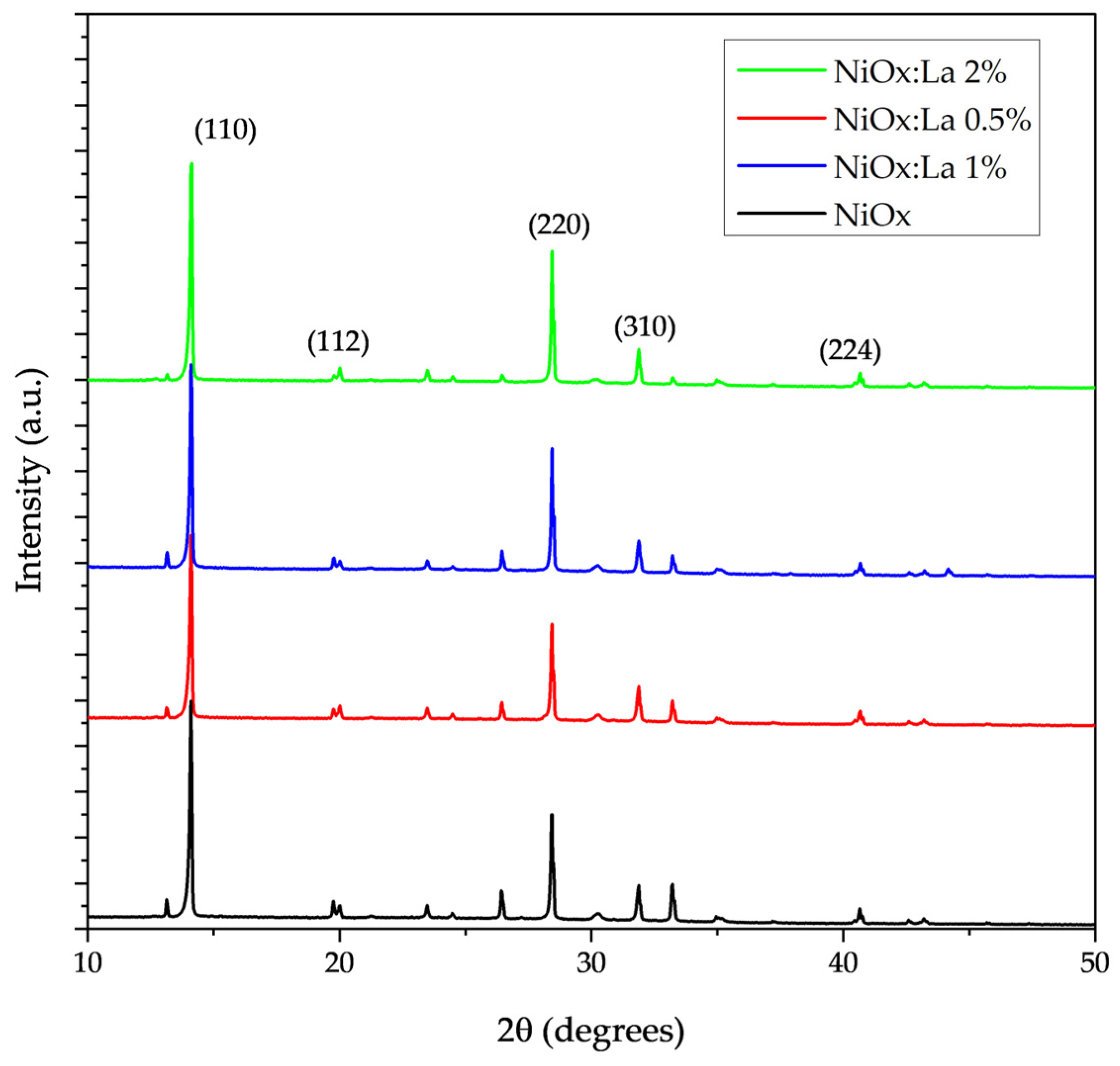
3.4.2. XRD Characterization

X-ray diffraction (XRD) was used to evaluate the crystal structure of PVK (MAPbI3) layers deposited on NiOx-based HTL variations. From the XRD patterns, the main diffraction peaks of MAPbI3 were observed at 2θ positions of 14.1° (110), 20.0° (112), 28.5° (220), 31.8° (310), and 40.6° (224) (Figure 10). No peak shifts were detected in any variation compared to the pristine material, indicating that the PVK crystal structure remained unchanged. This result also suggests that La3+ incorporation in NiOx does not introduce noticeable lattice strain in PVK and that phase purity is maintained. No diffraction peaks associated with La were observed in any of the variations, indicating no evidence of a separate crystalline phase formed by the La.
The Scherrer equation was used to determine the crystallite size based on the (110) peak, yielding values of 63.6 nm (NiOx), 64.8 nm (NiOx:La 0.5%), 68.2 nm (NiOx:La 1%), and 64.0 nm (NiOx:La 2%) (Figure S11). These results showed that the PVK crystallite size changes only marginally upon La modification, indicating that the perovskite’s basic crystalline unit remains essentially unchanged and that La3+ has little effect on nucleation or crystal growth [54,55]. In contrast, SEM revealed a ≈ 5% increase in grain size for the NiOx:La 0.5%/PVK film relative to NiOx/PVK, implying that La chiefly promotes grain coalescence rather than crystallite enlargement. Apart from this modest grain coarsening, La addition did not markedly alter the PVK layer’s crystallinity, grain-size distribution, or phase purity [56,57,58].
The lattice parameters of the PVK layers grown on the various HTLs are summarized in Table S7. The a and b parameters were essentially unchanged for all HTLs, whereas the c increased by ~1.8%, particularly for NiOx:La 2% relative to pristine NiOx. Thus, low La3+ concentrations did not measurably affect the PVK lattice, but at 2% La3+ a structural response appeared, likely arising from higher interfacial stress or partial La diffusion into the PVK, both of which could drive lattice expansion.

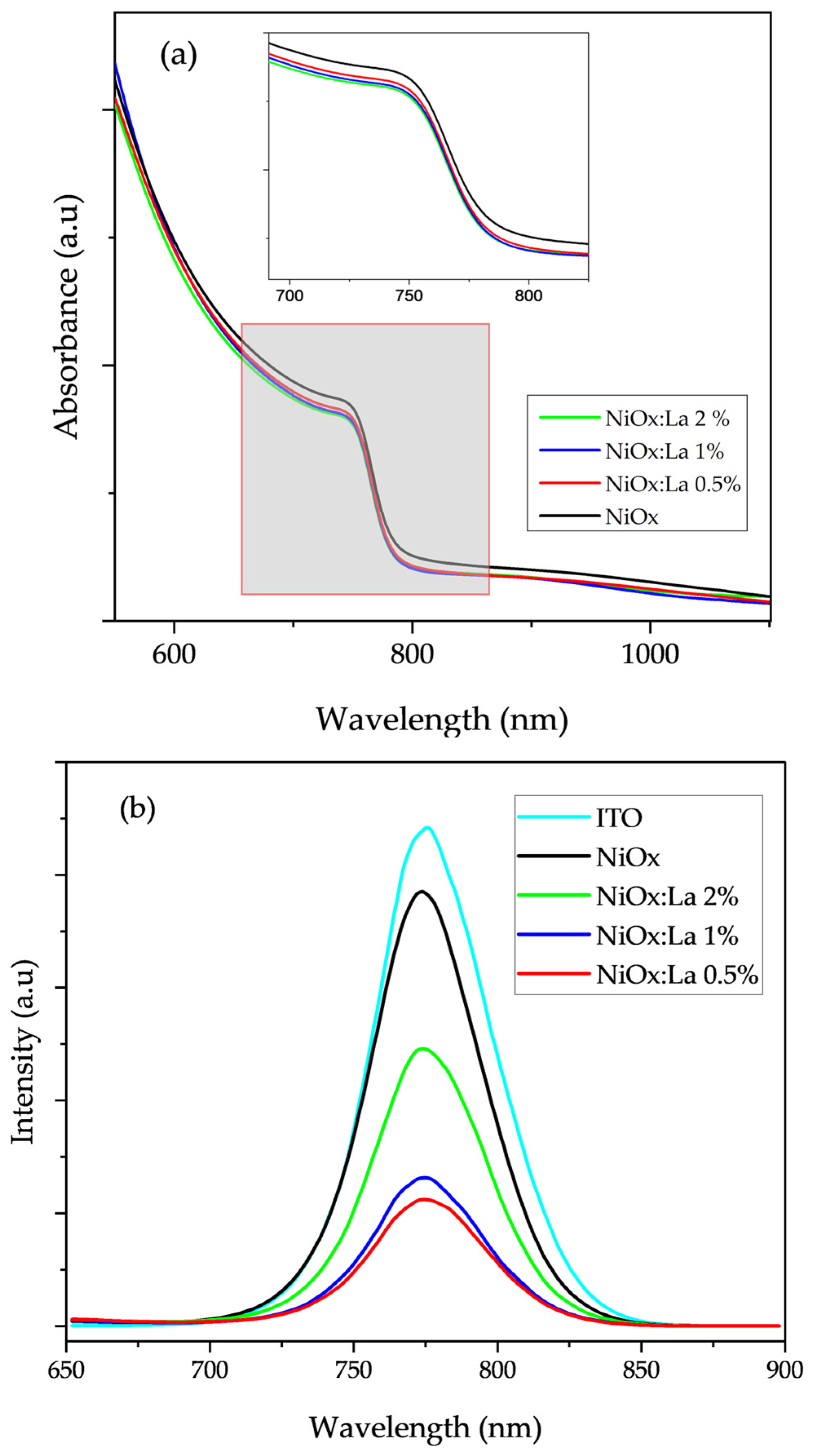
3.4.3. Optical Characterization

To assess whether La-modified NiOx altered the optical properties of the perovskite (PVK), we recorded absorbance spectra from 600 to 1100 nm for PVK layers grown on pristine NiOx and on NiOx:La. The UV–vis curves were indistinguishable (Figure 11a), and Tauc analysis yielded the same band-gap energy of 1.60 eV for PVK on both films (NiOx and NiOx:La 0.5%) (Figure S12) [17,59]. These results show that introducing 0.5% La in NiOx does not affect the PVK fundamental optical properties, consistent with its unchanged composition, phase, and band structure.
The photoluminescence (PL) spectra of PVK deposited on the various NiOx-based HTLs revealed how efficiently holes were extracted at the HTL/PVK interface: stronger PL quenching denotes better charge extraction. As seen in Figure 11b, La modification improved this process, with NiOx:La 0.5% showing the greatest quenching, followed closely by NiOx:La 1%. The PL peaks coincided with the PVK optical band-gap, and no peak shifts were observed, confirming that the absorber’s defect density and composition remained unchanged. The quenching hierarchy indicates that NiOx:La 0.5% most effectively removes photogenerated holes, suppressing electron–hole recombination. This result points to superior defect passivation in NiOx:La 0.5% and is consistent with EIS data that show lower interfacial resistance for this film. Accordingly, devices incorporating NiOx:La 0.5% delivered the highest FF and PCE among the variations tested [60].
NiOx and NiOx:La 0.5% HTLs were examined by cyclic voltammetry in a K3[Fe(CN)6] electrolyte to estimate their valence-band (HOMO) energies. Both films showed onset potentials that corresponded to −5.16 to −5.20 eV, matching reported values for pristine NiOx [35]; any La-induced shift therefore lies below the resolution of this technique. Figure S13 compiles these data into an energy-level diagram for the cell, combining literature values with the HOMO position determined here for NiOx:La 0.5% [61].

3.5. Stability

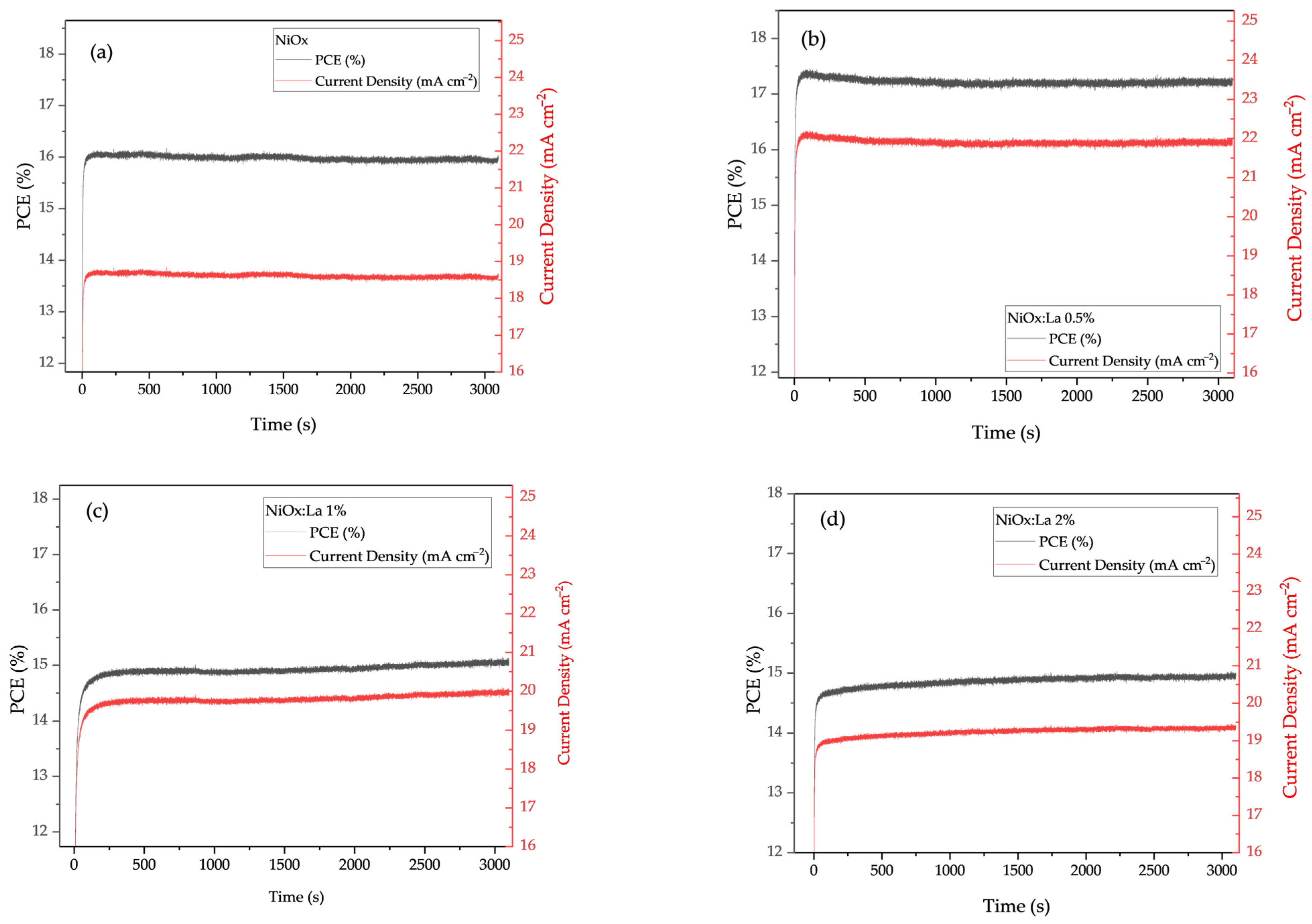
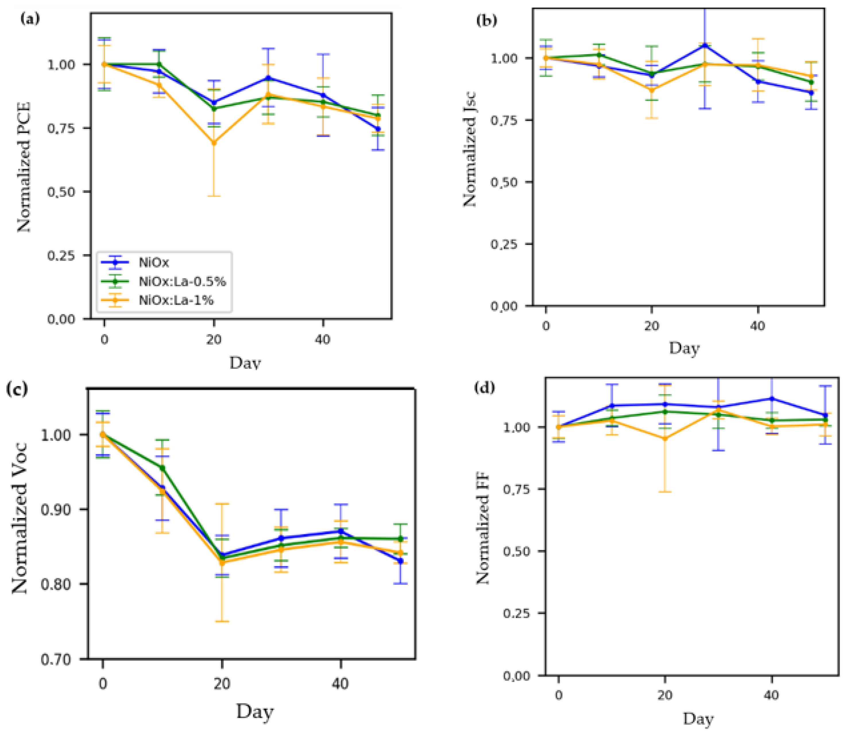
3.5.1. Stability of Cell Photovoltaic Parameters

The stability of 20 solar cells (ITO/NiOx/PVK/PCBM/Ag) was evaluated over 50 days. All devices were unencapsulated and stored in the dark under an atmosphere of nitrogen at room temperature (20 ± 2) and monitored every seven days. By removing illumination, bias, moisture, and encapsulant chemistry, the method singles out intrinsic instabilities (ion migration, defect growth, and interface reactions) that also operate, though more slowly, in fully packaged modules. Hence, improvements observed here translate directly to real world operational lifetimes once standard encapsulation and outdoor stresses are added [44].
Figure 12 illustrates the evolution of the normalized PV parameters with their respective error bars. All three variants followed a similar three-stage trend. The largest efficiency loss occurred between days 10 and 20, most notably for NiOx:La 1%. From day 20 to day 30 the PCE partially recovered in every variation, after which a gradual decline resumed until day 50, the drop being least severe for the NiOx:La cells. After 50 days the mean PCEs differed significantly: 13.08% for NiOx:La 0.5%, 12.85% for NiOx:La 1%, and 10.99% for pristine NiOx, corresponding to retention values of 80%, 79%, and 75%, respectively (Tables S8 and S9). The initial degradation phase is commonly attributed to ion migration in the perovskite and defect formation at the interfaces; the mid-term recovery is often ascribed to self-healing or lattice relaxation that restores charge transport [62]. The final slow decay is consistent with defect accumulation and perovskite decomposition [63].
Voc exhibited the largest degradation of any photovoltaic parameter, falling by ≈ 15% in all variants during the 50-day test (Tables S10 and S11). Such losses in inverted PSCs are generally linked to enhanced non-radiative recombination arising from defect generation, ion migration, and perovskite degradation [64].
The largest percentage decrease in Jsc was observed in NiOx (13.93%), whereas NiOx:La 0.5% and NiOx:La 1% showed smaller, statistically indistinguishable drops (−9.7% and −7.3%, respectively) (Tables S12 and S13). By contrast, the fill factor (FF) remained largely unchanged across all three cell variations at the end of 50 days.
Thus, the noticeable drop in Voc across all variations suggests that charge recombination became significant during the monitoring period, reducing the device’s built-in potential. Even so, the NiOx:La 0.5% cell retained better stability, implying that the optimal La modification partly suppresses defect formation and recombination, thereby sustaining a higher PCE.

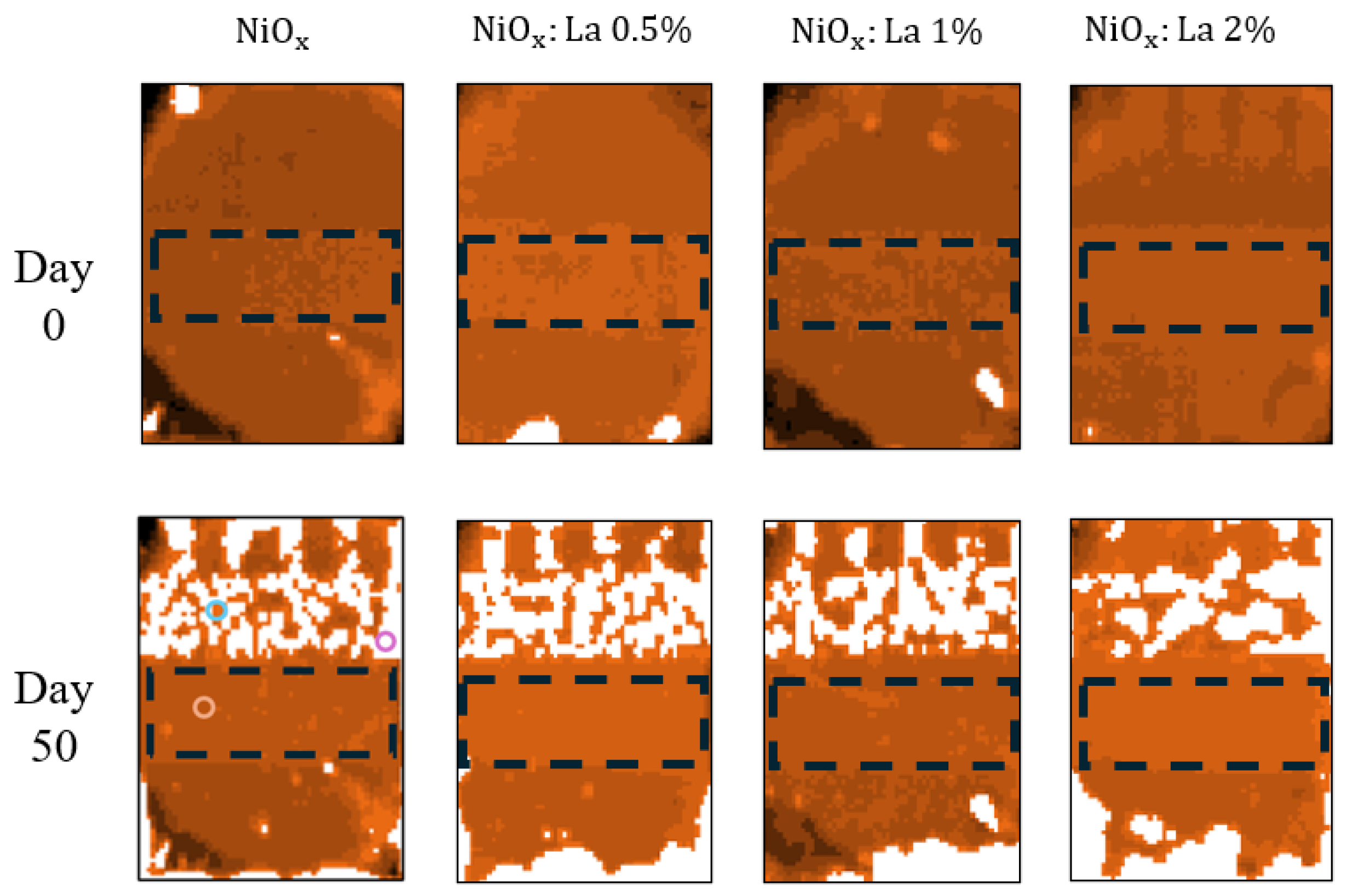
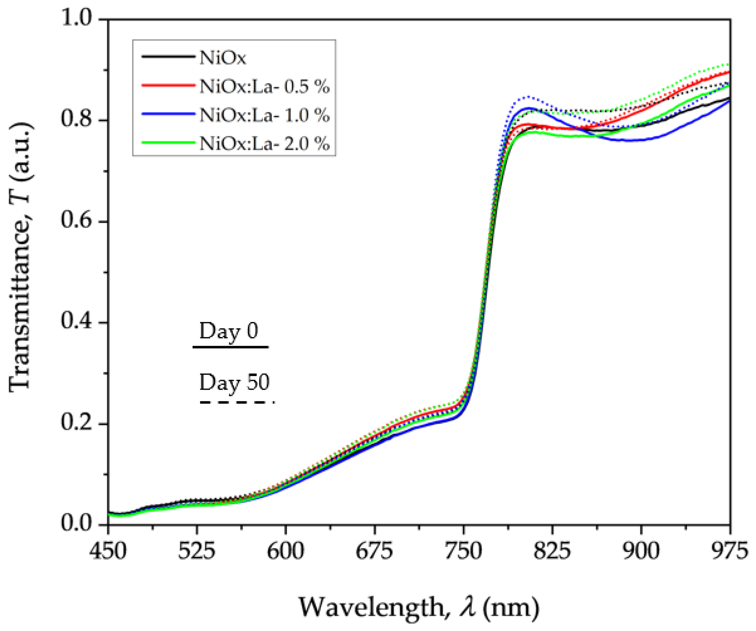
3.5.2. Stability of PVK in ITO/HTL/PVK

PVK layers deposited on the four types of HTLs were characterized using a hyperspectral camera SPECIM IQ that generated images of 256,000 pixels across 204 bands in the UV–vis–NIR range (397–1000 nm). This information has been used to monitor the changes in the optical absorption of the PVK layer for each case. Transmittance spectra were obtained over a region of interest (ROI) that covered the active zone of samples, marked from day 0 to day 50 (Figure 13 and Figure 14).
The integrated absorbance of the PVK layer declined by 2.03% (NiOx:La 0.5%), 3.67% (NiOx), 4.02% (NiOx:La 1%), and 4.55% (NiOx:La 2%) over 50 days (Table S14). Expressed relative to the NiOx, the loss for NiOx:La 0.5% was 81% smaller, implying that this HTL most effectively mitigated light-absorption degradation, typically caused by moisture ingress, defect generation, and interfacial reactions in IPSCs [65]. The superior optical retention agreed with the PV stability data, where the NiOx:La 0.5% cell showed the smallest declines in Jsc, FF, and PCE. The false-color images at 720 nm (Figure 13) confirm this behavior: of the ~1200 analyzed pixels (dashed area), all La-modified layers started with comparable PVK optical homogeneity (~97.5%), slightly higher than for pristine NiOx (96.3%), and none of the HTLs exhibited a significant change after 50 days (Table S15). Finally, Tauc plots for PVK/NiOx and PVK/NiOx:La 0.5% measured on days 0 and 50 show identical band gap values within the experimental error (Figure S14), indicating that the PVK composition and crystal structure remained stable throughout the test.
Returning to devices’ stability, despite a ~15% drop in Voc over 50 days, the NiOx:La 0.5% device retained 81% of its initial PCE, whereas pristine NiOx device kept only 75% (Figure 12). The cell stability test was conducted in the dark, at open circuit, under dry N2. These conditions strongly attenuate, though do not completely eliminate, the photo- and field-assisted halide reactions that drive Ag+ diffusion from the metal electrode into the PVK. Consequently, the efficiency loss is most plausibly attributed to intrinsic processes such as defect accumulation and slow ion redistribution, with any Ag-related degradation expected to be far less severe than under illuminated or biased [66]. Direct confirmation will require future cross-sectional analyses, e.g., SEM/EDX or TOF-SIMS depth profiling, of aged versus fresh devices to map the Ag distribution across the electrode/transport layer interface. This view is supported by the Voc trend and by hyperspectral-absorbance maps, which show that the smaller optical absorption loss in the NiOx:La 0.5%/PVK stack coincides with better preservation of Jsc and overall PCE. La modification therefore confers a measurable stability advantage, although further gains will require encapsulation and interfacial engineering to suppress both intrinsic and Ag-migration pathways over the long term.

4. Conclusions

This work demonstrates that La-modified NiOx prepared by electrochemical deposition is an effective hole-transport layer for inverted perovskite solar cells (IPSCs). The optimal composition, NiOx:La 0.5%, delivered a champion PCE of 20.08%, a sizeable improvement over pristine NiOx arising from enhanced charge transport, lower recombination losses, and more efficient extraction, as confirmed by EIS, Mott–Schottky, and steady-state PL measurements. X-ray photoelectron spectroscopy (XPS) showed that La was successfully incorporated into the NiOx lattice, an increase in the Ni3+/Ni3+ ratio, and also that a valence band shift was present. This suggests the formation of oxygen vacancies and increased hole concentration, which may contribute to the increase in p-type conductivity, and hence, the improvement of photovoltaic performance. SEM showed only a ~5% grain-size enlargement for the PVK on NiOx:La 0.5%, indicating that the efficiency gain stemmed mainly from improved electronic properties of the HTL rather than major changes in PVK morphology. Stability tests on non-encapsulated cells stored in the dark under an inert atmosphere showed that the NiOx:La 0.5% device retained 80% of its initial efficiency after 50 days, compared with 75% for pristine NiOx cell; hyperspectral imaging likewise indicated a superior 98% preservation of the PVK’s optical absorption. Overall, electrodeposited La-modified NiOx emerges as a reproducible, easily obtained HTL that pairs high efficiency with promising operational stability and merits further optimization through interface engineering.

Supplementary Materials

The following supporting information can be downloaded at https://www.mdpi.com/article/10.3390/en18143590/s1. Figure S1. ITO glass substrates coated with (a) NiOx and (b) NiOx:La. Figure S2. XPS wide-scan spectra between 0 to 1200 eV: (a) NiOx (b) NiOx:La 0.5% on ITO substrates. Figure S3. Water contact angle on (a) pristine NiOx (b) NiOx:La 0.5% (c) NiOx:La 1% (d) NiOx:La 2%. Figure S4. (a) Valence Band (VB) spectra by XPS of NiOx and (b) its elucidation by the region near Ef. Figure S5. (a) Valence Band (VB) XPS spectra of NiOx:La 0.5% (b) and its elucidation from the region near Ef. Figure S6. Cross-sectional view of SEM images of the IPSC (ITO/NiOx:La/PVK/PCBM/Ag) (a) Pristine NiOx (b) NiOx:La 0.5% (c) NiOx:La 1% (d) NiOx:La 2%. Figure S7. J-V curves of IPSCs with NiOx or NiOx:La as HTL Measurements taken for freshly fabricated cells. AM 1.5G sunlight (100 mW cm−2), with a potential sweep from −0.1 to 1.1 V at 50 mV/s. N = 20. Figure S8. Box plots of the IPSCs with HTL variations (a) Serie Resistance (Rs) (b) Shunt Resistance (Rsh). Figure S9. Elemental mapping by SEM-EDS of the NiOx film showing the spatial distribution of (a) O Kα1, (b) Ni Lα1,2, and (c) In Mζ (d) EDS mapping sum spectrum of a NiOx. Figure S10. Elemental mapping by SEM-EDS of the NiOx:La (30%) film showing the spatial distribution of (a) O Kα1, (b) Ni Lα1,2, (c) La Mα and (d) In Mζ (e) EDS mapping sum spectrum of a NiOx:La. Figure S11. XRD patterns of PVK layers on NiOx based HTLs, crystalite size of (a) NiOx (b) NiOx:La 0.5% (c) NiOx:La 1% (d) NiOx:La 2%. Figure S12. Tauc plot modification (a) NiOx/PVK (b) NiOx:La 0.5%/PVK. Figure S13. Cyclic voltammetry used to estimate the HOMO level of HTLs: (a) NiOx, (b) NiOx:La 0.5%, (c) NiOx:La 1%, (d) NiOx:La 2% and (e) a schematic of energy levels in the IPSC layers. Figure S14. Tauc Plots for PVK on NiOx and NiOx:La 0.5% for Day 0 and 50. Table S1. Elemental quantification of NiOx and NiOx:La 0.5% films. Table S2. XPS binding energy and peak fitting parameters for NiOx and NiOx:La 0.5%. Table S3. Summary of the carrier density values and slopes from the Mott-Schottky plots. Table S4. P-test to compare the photovoltaic parameters of solar cells based on NiOx:La. Each test compares the parameter for pristine NiOx with the La variation. (a) PCE, (b) Jsc, (c) Voc and (d) FF. N = 20. Table S5. Summary of Series Resistance (Rs) and Shunt Resistance (Rsh) for each HTL modification of IPSC on Day 0. Table S6. Summary of equivalent circuit elements for the IPSCs with different HTLs. Table S7. Lattice parameters of PVK layer deposited on each type of HTL. Table S8. Statistical p-value and Comparison of PCE between Pristine NiOx and NiOx:La 0.5%. Table S9. Statistical p-value and Comparison of PCE between Pristine NiOx and NiOx:La 1%. Table S10. Statistical p-value and Comparison of Voc between Pristine NiOx and NiOx:La 0.5%. Table S11. Statistical p-value and Comparison of Voc between Pristine NiOx and NiOx:La 1%. Table S12. Statistical p-value and Comparison of Jsc between Pristine NiOx and NiOx:La 1%. Table S13. Statistical p-value and Comparison of Jsc between Pristine NiOx and NiOx:La 1%. Table S14. Summary of alfa: ln(1/T) of ITO/HTL/PVK modifications. Table S15. Percentage of homogeneity according to the standard deviation of 1200 pixels of ITO/HTL/PVK. Equation (S1). Mott-Schottky equation.

Author Contributions

The manuscript was written through contributions from all authors. Below, the contribution of each author is detailed: L.A.-D.: writing—original draft, writing—review and editing, data curation, investigation, methodology, formal analysis. M.G.-H.: conceptualization, investigation. S.E.R.: writing—review and editing, conceptualization, investigation. J.A.R.-R.: writing—review and editing, conceptualization, investigation. P.O.: writing—review and editing, writing—original draft, investigation, funding acquisition. M.T.C.: writing—review and editing, writing—original draft, supervision, project administration, methodology, investigation, funding acquisition, formal analysis, conceptualization. All authors have read and agreed to the published version of the manuscript.

Funding

This project was funded by the Universidad de los Andes (Project INV-2025-213-3345), and Universidad de América (IHU-014).

Data Availability Statement

Data is contained within the article and the Supplementary Material. Any additional data will be available upon request.

Acknowledgments

The authors thank the Department of Chemistry and the Department of Chemical Engineering for their support. M.T.C. and L.A.-D. thank the Faculty of Science (Project INV-2025-213-3345). The authors thank the Universidad de América Foundation for funding through grant IHU-014. The authors acknowledge the instruments and scientific and technical assistance of the MicroCore Microscopy Core at the Universidad de Los Andes (vice-presidency for research and creation).

Conflicts of Interest

The authors declare no conflicts of interest.

References

  1. Kojima, A.; Teshima, K.; Shirai, Y.; Miyasaka, T. Organometal halide perovskites as visible-light sensitizers for photovoltaic cells. J. Am. Chem. Soc. 2009, 131, 6050–6051. [Google Scholar] [CrossRef] [PubMed]
  2. Yang, C.; Hu, W.; Liu, J.; Han, C.; Gao, Q.; Mei, A.; Zhou, Y.; Guo, F.; Han, H. Achievements, challenges, and future prospects for industrialization of perovskite solar cells. Light Sci. Appl. 2024, 13, 227. [Google Scholar] [CrossRef] [PubMed]
  3. Suresh Kumar, N.; Chandra Babu Naidu, K. A review on perovskite solar cells (PSCs), materials and applications. J. Mater. 2021, 7, 940–956. [Google Scholar] [CrossRef]
  4. Vivo, P.; Salunke, J.K.; Priimagi, A. Hole-transporting materials for printable perovskite solar cells. Materials 2017, 10, 1087. [Google Scholar] [CrossRef]
  5. Cai, X.; Hu, T.; Hou, H.; Zhu, P.; Liu, R.; Peng, J.; Luo, W.; Yu, H. A review for nickel oxide hole transport layer and its application in halide perovskite solar cells. Mater. Today Sustain. 2023, 23, 100438. [Google Scholar] [CrossRef]
  6. Zhang, H.; Shi, Y.; Yan, F.; Wang, L.; Wang, K.; Xing, Y.; Dong, Q.; Ma, T. A dual functional additive for the HTM layer in perovskite solar cells. Chem. Commun. 2014, 50, 5020–5022. [Google Scholar] [CrossRef]
  7. Song, Z.; Watthage, S.C.; Phillips, A.B.; Heben, M.J. Pathways toward high-performance perovskite solar cells: Review of recent advances in organo-metal halide perovskites for photovoltaic applications. J. Photonics Energy 2016, 6, 022001. [Google Scholar] [CrossRef]
  8. Saha, N.; Brunetti, G.; Armenise, M.N.; Di Carlo, A.; Ciminelli, C. Modeling Highly Efficient Homojunction Perovskite Solar Cells With Graphene-TiO2 Nanocomposite as the Electron Transport Layer. IEEE J. Photovoltaics 2023, 13, 705–710. [Google Scholar] [CrossRef]
  9. Agresti, A.; Pazniak, A.; Pescetelli, S.; Di Vito, A.; Rossi, D.; Pecchia, A.; Auf der Maur, M.; Liedl, A.; Larciprete, R.; Kuznetsov, D.V.; et al. Titanium-carbide MXenes for work function and interface engineering in perovskite solar cells. Nat. Mater. 2019, 18, 1228–1234. [Google Scholar] [CrossRef]
  10. Pitchaiya, S.; Natarajan, M.; Santhanam, A.; Asokan, V.; Yuvapragasam, A.; Madurai Ramakrishnan, V.; Palanisamy, S.E.; Sundaram, S.; Velauthapillai, D. A review on the classification of organic/inorganic/carbonaceous hole transporting materials for perovskite solar cell application. Arab. J. Chem. 2020, 13, 2526–2557. [Google Scholar] [CrossRef]
  11. Kaya, I.C.; Akin, S.; Sonmezoglu, S. Future Perspectives of Perovskite Solar Cells: Metal Oxide-Based Inorganic Hole-Transporting Materials; Elsevier: Amsterdam, The Netherlands, 2020; ISBN 9780128206287. [Google Scholar]
  12. Park, H.; Chaurasiya, R.; Jeong, B.H.; Sakthivel, P.; Park, H.J. Nickel Oxide for Perovskite Photovoltaic Cells. Adv. Photonics Res. 2021, 2, 2000178. [Google Scholar] [CrossRef]
  13. Chen, X.; Xu, L.; Chen, C.; Wu, Y.; Bi, W.; Song, Z.; Zhuang, X.; Yang, S.; Zhu, S.; Song, H. Rare earth ions doped NiOx hole transport layer for efficient and stable inverted perovskite solar cells. J. Power Sources 2019, 444, 227267. [Google Scholar] [CrossRef]
  14. Hu, Z.; Chen, D.; Yang, P.; Yang, L.; Qin, L.; Huang, Y.; Zhao, X. Sol-gel-processed yttrium-doped NiO as hole transport layer in inverted perovskite solar cells for enhanced performance. Appl. Surf. Sci. 2018, 441, 258–264. [Google Scholar] [CrossRef]
  15. Teo, S.; Guo, Z.; Xu, Z.; Zhang, C.; Kamata, Y.; Hayase, S.; Ma, T. The Role of Lanthanum in a Nickel Oxide-Based Inverted Perovskite Solar Cell for Efficiency and Stability Improvement. ChemSusChem 2019, 12, 518–526. [Google Scholar] [CrossRef] [PubMed]
  16. Chappidi, V.R.; Nayak, S.K.; Kayesh, M.E.; Karim, M.A.; He, Y.; Islam, A.; Raavi, S.S.K. Elucidating the improved properties of defect engineered lanthanum-doped nickel oxide as hole-transport layer in triple-cation perovskite solar cells. Sol. Energy 2024, 281, 112888. [Google Scholar] [CrossRef]
  17. Park, I.J.; Kang, G.; Park, M.A.; Kim, J.S.; Seo, W.; Kim, D.H.; Zhu, K.; Park, T.; Kim, J.Y. Highly efficient and uniform 1 cm2 perovskite solar cells with an electrochemically deposited NiOx hole-extraction layer. Energy Mater. 2017, 10, 2660–2667. [Google Scholar] [CrossRef]
  18. Bogachuk, D.; Baretzky, C.; Eckert, J.; Yang, B.; Suo, J.; Dangudubiyyam, U.K.; Loukeris, G.; Mohammadzadeh, H.; Kluska, S.; Kohlstädt, M.; et al. Rethinking Electrochemical Deposition of Nickel Oxide for Photovoltaic Applications. Sol. RRL 2024, 8, 2300750. [Google Scholar] [CrossRef]
  19. Shojaie, A.F.; Loghmani, M.H. La3+ and Zr4+ co-doped anatase nano TiO2 by sol-microwave method. Chem. Eng. J. 2010, 157, 263–269. [Google Scholar] [CrossRef]
  20. González-Hernández, M.; Reyes, S.E.; Erazo, E.A.; Ortiz, P.; Cortés, M.T. Enhanced inverted perovskite solar cells via indium doped nickel oxide as hole transport layer. Sol. Energy 2024, 276, 112657. [Google Scholar] [CrossRef]
  21. Imran, M.; Coskun, H.; Khan, N.A.; Ouyang, J. Role of annealing temperature of nickel oxide (NiOx) as hole transport layer in work function alignment with perovskite. Appl. Phys. A 2021, 127, 117. [Google Scholar] [CrossRef]
  22. Blume, A.R.; Calvet, W.; Ghafari, A.; Mayer, T.; Knop-Gericke, A.; Schlögl, R. Structural and chemical properties of NiOx thin films: The role of oxygen vacancies in NiOOH formation in a H2O atmosphere. Phys. Chem. Chem. Phys. 2023, 25, 25552–25565. [Google Scholar] [CrossRef]
  23. Sharma, R.; Yadav, K. Effect of lattice defects on the structural and optical properties of Ni1XAgXO (where X = 0.0, 0.01, 0.03, 0.05, 0.10 and 0.15) nanoparticles. Appl. Phys. A 2018, 124, 88. [Google Scholar] [CrossRef]
  24. Geng, X.; Lahem, D.; Zhang, C.; Li, C.J.; Olivier, M.G.; Debliquy, M. Visible light enhanced black NiO sensors for ppb-level NO2 detection at room temperature. Ceram. Int. 2019, 45, 4253–4261. [Google Scholar] [CrossRef]
  25. Wu, Y.; Chang, C.; Chiu, F.; Yang, S. Efficient and stable perovskite solar cells using manganese-doped nickel oxide as the hole transport layer. RSC Adv. 2022, 12, 22984–22995. [Google Scholar] [CrossRef]
  26. Fingerle, M.; Tengeler, S.; Calvet, W.; Jaegermann, W.; Mayer, T. Sputtered Nickel Oxide Thin Films on n-Si(100)/SiO2 Surfaces for Photo-Electrochemical Oxygen Evolution Reaction (OER): Impact of Deposition Temperature on OER Performance and on Composition before and after OER. J. Electrochem. Soc. 2020, 167, 136514. [Google Scholar] [CrossRef]
  27. Cole, R.J.; Macdonald, B.F.; Weightman, P. Relative core level shifts in XPS: A theoretical study. J. Electron Spectrosc. Relat. Phenom. 2002, 125, 147–152. [Google Scholar] [CrossRef]
  28. Akalin, S.A.; Erol, M.; Uzunbayir, B.; Oguzlar, S.; Yildirim, S.; Gokdemir Choi, F.P.; Gunes, S.; Yilmazer Menda, U.D.; Mendes, M.J. Physically-Deposited Hole Transporters in Perovskite PV: NiOx Improved with Li/Mg Doping. Adv. Mater. Technol. 2024, 9, 2301760. [Google Scholar] [CrossRef]
  29. Grządziel, L.; Krzywiecki, M.; Szwajca, A.; Sarfraz, A.; Genchev, G.; Erbe, A. Detection of intra-band gap defects states in spin-coated sol-gel SnOx nanolayers by photoelectron spectroscopies. J. Phys. D Appl. Phys. 2018, 51, 315301. [Google Scholar] [CrossRef]
  30. Batzill, M.; Diebold, U. The surface and materials science of tin oxide. Prog. Surf. Sci. 2005, 79, 47–154. [Google Scholar] [CrossRef]
  31. Abfalterer, A.; Shamsi, J.; Kubicki, D.J.; Savory, C.N.; Xiao, J.; Divitini, G.; Li, W.; Macpherson, S.; Gałkowski, K.; Macmanus-Driscoll, J.L.; et al. Colloidal Synthesis and Optical Properties of Perovskite-Inspired Cesium Zirconium Halide Nanocrystals. ACS Mater. Lett. 2020, 2, 1644–1652. [Google Scholar] [CrossRef]
  32. Sahoo, L.; Behera, S.A.; Achary, P.G.R.; Parida, S.K. Impedance spectroscopy and optical properties of lanthanum-modified Bi2FeMnO6 for NTC thermistor applications. Mater. Adv. 2025, 6, 1455–1467. [Google Scholar] [CrossRef]
  33. Malavekar, D.B.; Magdum, V.V.; Khot, S.D.; Kim, J.H.; Lokhande, C.D. Doping of rare earth elements: Towards enhancing the electrochemical performance of pseudocapacitive materials. J. Alloys Compd. 2023, 960, 170601. [Google Scholar] [CrossRef]
  34. Han, D.; Jing, X.; Wang, J.; Yang, P.; Song, D.; Liu, J. Porous lanthanum doped NiO microspheres for supercapacitor application. J. Electroanal. Chem. 2012, 682, 37–44. [Google Scholar] [CrossRef]
  35. Iskandar, F.; Abdillah, O.B.; Stavila, E.; Aimon, A.H. The influence of copper addition on the electrical conductivity and charge transfer resistance of reduced graphene oxide (rGO). N. J. Chem. 2018, 42, 16362–16371. [Google Scholar] [CrossRef]
  36. Soltani-Ahmadi, M.; Muhler, H. Impedance Spectroscopy. In Electrochemical Impedance Spectroscopy; Wiley-Interscience: Hoboken, NJ, USA, 2020; ISBN 9780470041406. [Google Scholar]
  37. Randviir, E.P.; Banks, C.E. Electrochemical Impedance Spectroscopy—An Overview of bioanalytical applications. Anal. Methods 2013, 5, 1098–1115. [Google Scholar] [CrossRef]
  38. Digdaya, I.A.; Rodriguez, P.P.; Ma, M.; Adhyaksa, G.W.P.; Garnett, E.C.; Smets, A.H.M.; Smith, W.A. Engineering the kinetics and interfacial energetics of Ni/Ni-Mo catalyzed amorphous silicon carbide photocathodes in alkaline media. J. Mater. Chem. A 2016, 4, 6842–6852. [Google Scholar] [CrossRef]
  39. Saki, Z.; Sveinbjörnsson, K.; Boschloo, G.; Taghavinia, N. The Effect of Lithium Doping in Solution-Processed Nickel Oxide Films for Perovskite Solar Cells. ChemPhysChem 2019, 20, 3322–3327. [Google Scholar] [CrossRef] [PubMed]
  40. Natu, G.; Hasin, P.; Huang, Z.; Ji, Z.; He, M.; Wu, Y. Valence band-edge engineering of nickel oxide nanoparticles via cobalt doping for application in p-type dye-sensitized solar cells. ACS Appl. Mater. Interfaces 2012, 4, 5922–5929. [Google Scholar] [CrossRef]
  41. Bagade, S.S.; Barik, S.B.; Malik, M.M.; Patel, P.K. Impact of band alignment at interfaces in perovskite-based solar cell devices. Mater. Today Proc. 2023, in press. [Google Scholar] [CrossRef]
  42. Crovetto, A.; Hansen, O. What is the band alignment of Cu2ZnSn(S,Se)4 solar cells? Sol. Energy Mater. Sol. Cells 2017, 169, 177–194. [Google Scholar] [CrossRef]
  43. Latrous, A.R.; Mahamdi, R.; Touafek, N.; Pasquinelli, M. Conduction Band Offset Effect on the Cu2ZnSnS4 Solar Cells Performance. Ann. Chim.-Sci. Mater. 2021, 45, 431–437. [Google Scholar] [CrossRef]
  44. Khenkin, M.V.; Katz, E.A.; Abate, A.; Bardizza, G.; Berry, J.J.; Brabec, C.; Brunetti, F.; Bulović, V.; Burlingame, Q.; Di Carlo, A.; et al. Consensus statement for stability assessment and reporting for perovskite photovoltaics based on ISOS procedures. Nat. Energy 2020, 5, 35–49. [Google Scholar] [CrossRef]
  45. Contreras-Bernal, L.; Ramos-Terrón, S.; Riquelme, A.; Boix, P.P.; Idígoras, J.; Mora-Seró, I.; Anta, J.A. Impedance analysis of perovskite solar cells: A case study. J. Mater. Chem. A 2019, 7, 12191–12200. [Google Scholar] [CrossRef]
  46. Hörantner, M.T.; Nayak, P.K.; Mukhopadhyay, S.; Wojciechowski, K.; Beck, C.; McMeekin, D.; Kamino, B.; Eperon, G.E.; Snaith, H.J. Shunt-Blocking Layers for Semitransparent Perovskite Solar Cells. Adv. Mater. Interfaces 2016, 3, 1500837. [Google Scholar] [CrossRef]
  47. Von Hauff, E.; Klotz, D. Impedance spectroscopy for perovskite solar cells: Characterisation, analysis, and diagnosis. J. Mater. Chem. C 2022, 10, 742–761. [Google Scholar] [CrossRef]
  48. Ghahremanirad, E.; Almora, O.; Suresh, S.; Drew, A.A.; Chowdhury, T.H.; Uhl, A.R. Beyond Protocols: Understanding the Electrical Behavior of Perovskite Solar Cells by Impedance Spectroscopy. Adv. Energy Mater. 2023, 13, 2204370. [Google Scholar] [CrossRef]
  49. Ahmad, Z.; Mishra, A.; Abdulrahim, S.M.; Touati, F. Electrical equivalent circuit (EEC) based impedance spectroscopy analysis of HTM free perovskite solar cells. J. Electroanal. Chem. 2020, 871, 114294. [Google Scholar] [CrossRef]
  50. Muscarella, L.A.; Hutter, E.M.; Sanchez, S.; Dieleman, C.D.; Savenije, T.J.; Hagfeldt, A.; Saliba, M.; Ehrler, B. Crystal Orientation and Grain Size: Do They Determine Optoelectronic Properties of MAPbI3 Perovskite? J. Phys. Chem. Lett. 2019, 10, 6010–6018. [Google Scholar] [CrossRef]
  51. Gedamu, D.; Asuo, I.M.; Benetti, D.; Basti, M.; Ka, I.; Cloutier, S.G.; Rosei, F.; Nechache, R. Solvent-Antisolvent Ambient Processed Large Grain Size Perovskite Thin Films for High-Performance Solar Cells. Sci. Rep. 2018, 8, 12885. [Google Scholar] [CrossRef]
  52. Zheng, X.; Deng, Y.; Chen, B.; Wei, H.; Xiao, X.; Fang, Y.; Lin, Y.; Yu, Z.; Liu, Y.; Wang, Q.; et al. Dual Functions of Crystallization Control and Defect Passivation Enabled by Sulfonic Zwitterions for Stable and Efficient Perovskite Solar Cells. Adv. Mater. 2018, 30, 1803428. [Google Scholar] [CrossRef]
  53. Marand, Z.R.; Kermanpur, A.; Karimzadeh, F.; Barea, E.M.; Hassanabadi, E.; Anaraki, E.H.; Julián-López, B.; Masi, S.; Mora-Seró, I. Structural and electrical investigation of cobalt-doped NiOx/perovskite interface for efficient inverted solar cells. Nanomaterials 2020, 10, 872. [Google Scholar] [CrossRef] [PubMed]
  54. Chen, W.; Wu, Y.; Tu, B.; Liu, F.; Djurišić, A.B.; He, Z. Inverted planar organic-inorganic hybrid perovskite solar cells with NiOx hole-transport layers as light-in window. Appl. Surf. Sci. 2018, 451, 325–332. [Google Scholar] [CrossRef]
  55. Hou, D.; Zhang, J.; Gan, X.; Yuan, H.; Yu, L.; Lu, C.; Sun, H.; Hu, Z.; Zhu, Y. Pb and Li co-doped NiOx for efficient inverted planar perovskite solar cells. J. Colloid Interface Sci. 2020, 559, 29–38. [Google Scholar] [CrossRef]
  56. Du, T.; Macdonald, T.J.; Yang, R.X.; Li, M.; Jiang, Z.; Mohan, L.; Xu, W.; Su, Z.; Gao, X.; Whiteley, R.; et al. Additive-Free Low-Temperature Crystallization of Stable-FAPbI3 Perovskite. Adv. Mater. 2022, 34, 2107850. [Google Scholar] [CrossRef]
  57. Chen, W.; Liu, F.Z.; Feng, X.Y.; Djurišić, A.B.; Chan, W.K.; He, Z.B. Cesium Doped NiOx as an Efficient Hole Extraction Layer for Inverted Planar Perovskite Solar Cells. Adv. Energy Mater. 2017, 7, 1700722. [Google Scholar] [CrossRef]
  58. Da Silva, E.L.; Skelton, J.M.; Parker, S.C.; Walsh, A. Phase stability and transformations in the halide perovskite CsSnI3. Phys. Rev. B 2015, 91, 144107. [Google Scholar] [CrossRef]
  59. Hu, Z.; Lin, Z.; Su, J.; Zhang, J.; Chang, J.; Hao, Y. A Review on Energy Band-Gap Engineering for Perovskite Photovoltaics. Sol. RRL 2019, 3, 1900304. [Google Scholar] [CrossRef]
  60. Shalan, A.E.; Oshikiri, T.; Narra, S.; Elshanawany, M.M.; Ueno, K.; Wu, H.P.; Nakamura, K.; Shi, X.; Diau, E.W.G.; Misawa, H. Cobalt Oxide (CoOx) as an Efficient Hole-Extracting Layer for High-Performance Inverted Planar Perovskite Solar Cells. ACS Appl. Mater. Interfaces 2016, 8, 33592–33600. [Google Scholar] [CrossRef]
  61. Reyes, S.E.; González-Hernández, M.; Cortés, M.T.; Ortiz, P. Effect of NH4F surface treatment of electrodeposited NiOx on the properties and reproducibility of inverted perovskite solar cells. Surf. Interfaces 2025, 56, 105654. [Google Scholar] [CrossRef]
  62. Roose, B. Ion migration drives self-passivation in perovskite solar cells and is enhanced by light soaking. RSC Adv. 2021, 11, 12095–12101. [Google Scholar] [CrossRef]
  63. Lee, S.W.; Kim, S.; Bae, S.; Cho, K.; Chung, T.; Mundt, L.E.; Lee, S.; Park, S.; Park, H.; Schubert, M.C.; et al. UV Degradation and Recovery of Perovskite Solar Cells. Sci. Rep. 2016, 6, 38150. [Google Scholar] [CrossRef] [PubMed]
  64. Zhang, D.; Li, D.; Hu, Y.; Mei, A.; Han, H. Degradation pathways in perovskite solar cells and how to meet international standards. Commun. Mater. 2022, 3, 58. [Google Scholar] [CrossRef]
  65. Stoddard, R.J.; Dunlap-Shohl, W.A.; Qiao, H.; Meng, Y.; Kau, W.F.; Hillhouse, H.W. Forecasting the Decay of Hybrid Perovskite Performance Using Optical Transmittance or Reflected Dark-Field Imaging. ACS Energy Lett. 2020, 5, 946–954. [Google Scholar] [CrossRef]
  66. Besleaga, C.; Abramiuc, L.E.; Stancu, V.; Tomulescu, A.G.; Sima, M.; Trinca, L.; Plugaru, N.; Pintilie, L.; Nemnes, G.A.; Iliescu, M.; et al. Iodine Migration and Degradation of Perovskite Solar Cells Enhanced by Metallic Electrodes. J. Phys. Chem. Lett. 2016, 7, 5168–5175. [Google Scholar] [CrossRef] [PubMed]
Figure 1. XPS high-resolution spectra for (a,b) pristine NiOx and (c,d) NiOx:La 0.5%. The spectra were deconvoluted for (a) Ni 2p3/2, (c) Ni 2p3/2, and La 3d 3/2, La 3d 5/2; (b,d) O 1 s.
Energies 18 03590 g001
Figure 2. (a) Nyquist plots of NiOx, NiOx:La 0.5%, NiOx:La 1%, NiOx:La 2% layers on ITO obtained by EIS in 5 mM Fe2+/3+(CN)6 and 0.1 M KCl from 0.1 Hz to 100 kHz at 0.4 V. (b) Equivalent circuit to fit the data from (a).
Energies 18 03590 g002
Figure 3. Mott–Schottky plots of NiOx, NiOx:La 0.5%, NiOx:La 1% layers on ITO obtained by EIS in 5 mM Fe2+/3+(CN)6 and 0.1 M KCl. Na: Charge carrier density. Efb: flat band potential.
Energies 18 03590 g003
Figure 4. (a) Device architecture and (b) SEM cross-sectional image of the inverted Perovskite solar cell (IPSC) (ITO/HTL/CH3NH3PbI3/PCBM/BCP/Ag).
Energies 18 03590 g004
Figure 5. Box plots of the IPSCs with HTL based NiOx, NiOx:La 0.5%, NiOx:La 1%, and NiOx:La 2%, (a) PCE, (b) Jsc, (c) Voc, and (d) FF. The orange line corresponds to the median value and the red square to the mean value for each variation (20 devices per variation). Colored dots represent individual cell measurements.
Energies 18 03590 g005
Figure 6. J-V curves of the champion IPSCs with each HTL modification.
Energies 18 03590 g006
Figure 7. Maximum power point tracking (MPPT) of the champion devices for (a) NiOx, (b) NiOx:La 0.5%, (c) NiOx:La 1%, and (d) NiOx:La 2%.
Energies 18 03590 g007
Figure 8. (a) Nyquist diagram of IPSC for HTL modifications NiOx, NiOx:La 0.5%, NiOx:La 1%, NiOx:La 2%. (b) Equivalent circuit.
Energies 18 03590 g008aEnergies 18 03590 g008b
Figure 9. SEM top-view images and average grain size histograms of PVK layers deposited on NiOx based HTLs. (a) NiOx, (b) NiOx:La 0.5%, (c) NiOx:La 1%, (d) NiOx:La 2%.
Energies 18 03590 g009aEnergies 18 03590 g009b
Figure 10. XRD patterns of PVK layers on NiOx based HTLs.
Energies 18 03590 g010
Figure 11. (a) UV–vis absorption spectrum and (b) PL curves for PVK layers on ITO and on NiOx-based HTLs.
Energies 18 03590 g011
Figure 12. Fifty-day stability of photovoltaic parameters in IPSCs with NiOx-based HTLs. (n = 20) (a) PCE, (b) Jsc, (c) Voc, (d) FF.
Energies 18 03590 g012
Figure 13. False-color hyperspectral images (generated at 720 nm) of PVK in the configuration ITO/HTL/PVK. Different HTLs based on NiOx were evaluated at day 0 and day 50. The dotted box indicates the region of interest for spectrum acquisition.
Energies 18 03590 g013
Figure 14. Average transmittance spectra of PVK on different NiOx-based HTLs, measured on day 0 and day 50 over a region of interest of 1200 pixels in the active zone of the samples.
Energies 18 03590 g014
Table 1. Photovoltaic parameters of champion IPSC devices with NiOx, NiOx:La 0.5%, NiOx:La 1%, and NiOx:La 2% (day 0). Power conversion efficiency (PCE), open-circuit voltage (Voc), short-circuit current density (Jsc), and fill factor (FF).
HTLPCE (%)Voc (V)Jsc (mA cm−2)FF (%)
NiOx17.761.07623.1871.14
NiOx:La 0.5%20.081.08623.0680.12
NiOx:La 1%18.441.03623.0877.06
NiOx:La 2%15.241.02623.3363.65
Disclaimer/Publisher’s Note: The statements, opinions and data contained in all publications are solely those of the individual author(s) and contributor(s) and not of MDPI and/or the editor(s). MDPI and/or the editor(s) disclaim responsibility for any injury to people or property resulting from any ideas, methods, instructions or products referred to in the content.

