1. Introduction
DC-DC converters are an important part of switch-mode power supplies [
1,
2,
3]. They are used in both low- and high-power supply systems. The structures of DC-DC converters are described in many papers [
1,
4]. They include both isolated and non-isolated DC-DC converters. Each of these converters contains such components as transistors, diodes, inductors and capacitors. The number of these components and the values of their parameters may be different, but each of them is a source of power losses in the converter under consideration [
5,
6,
7].
A very important parameter of switch-mode power supplies is their energy efficiency [
8]. As demonstrated in the results from the papers [
9,
10,
11], the value of this parameter depends on the input voltage, load current, frequency and duty cycle of the control signal. In the components of DC-DC converters, there are conduction and switching losses [
12,
13].
The first of these types is related to the DC characteristics of these components. For transistors and diodes, conduction losses are the result of the voltage drop on the device operating in forward mode. In turn, for capacitors and inductors, they are the effect of the occurrence of parasitic resistances of these components [
14,
15]. Switching losses are related to the turning on and turning off of transistors and diodes or to hysteresis losses in the cores contained in inductors and transformers [
16]. Both groups of losses depend on the construction of the mentioned components and their junction temperature [
11,
17].
The junction temperature of semiconductor devices and passive components is higher than the ambient temperature due to the self-heating phenomenon and mutual thermal coupling between converter components placed on a common base [
18,
19,
20]. Thermal coupling occurs, among others, between diodes and IGBTs placed in the power module [
10,
21] and between the winding and the core of each inductor [
22,
23]. A change in the junction temperature of particular components causes a change in the values of parameters characterizing power losses in these components [
11,
24].
The design stage of a power electronic converter requires computer simulations to control power losses in its components and to manage its thermal performance. Such simulations need appropriate software and models of all the components of the system in a form acceptable in the used software. The commonly used programs for the circuit-level analysis of power electronic systems are SPICE [
25,
26] and PLECS [
27]. However, it is reported in many papers that due to significant differences in electrical and thermal time constants, the simulation duration is not acceptable. In the case of switch-mode power supplies, dedicated methods for increasing the speed of transient analysis simulations [
28,
29,
30] or averaged models are used, which allow the computation of the characteristics of such systems in a steady state using DC analysis [
9,
10,
17] or simplified transient simulations [
31]. Averaged models of selected power electronic converters are described, among others, in [
4,
5,
9,
32,
33]. Typically, in such models, losses in the system components are omitted [
4,
5] or described in a very simple form using linear resistors and omitting switching losses.
Self-heating phenomena and mutual thermal couplings can be included in computer analyses if special electrothermal models are used [
19,
34,
35]. These models are typically based on the classical Cauer or Foster network, with the parameter estimation procedure based on 3D FEM modeling [
36,
37] or transient thermal impedance measurements [
38]. In [
10], an averaged electrothermal model of a half-bridge converter including an IGBT module was formulated. The described model takes into account thermal phenomena occurring both in this module and in passive components.
The aim of the research presented in this paper is to formulate an averaged electrothermal model of a buck DC-DC converter including an IGBT module and to analyze the influence of the operating conditions of this converter on the losses in its components and their junction temperatures. New formulas describing dynamic power losses in semiconductor devices and in the inductor cores are proposed. Additionally, a method of taking into account the influence of power losses in the core and switching losses in semiconductor devices on the energy efficiency of the modeled DC-DC converter is proposed. The elaborated model has the form of subcircuits for SPICE software. The model was verified experimentally, and the obtained results of simulations were compared with the results obtained in PLECS using the model proposed by the producer of the IGBT module. The characteristics of the converter under test in the steady state were determined using the elaborated model and the model designed for PLECS software, illustrating the influence of selected factors on power losses in each component and their junction temperature, as well as the converter’s energy efficiency. It is shown that the use of the proposed averaged model makes it possible to obtain more accurate computation results and a shorter calculation time than those obtained using PLECS software. Through the use of the formulated model, the dependence of power losses in each component was calculated using DC analysis in different operating conditions. Also, the distribution of power losses in the analyzed converter was computed and discussed.
Section 2 describes the tested DC-DC converter. The form of the formulated converter model is described in
Section 3.
Section 4 presents the analysis results. Selected calculation results are compared with the measurement results.
3. Form of the Elaborated Model
The developed model of the buck converter belongs to the group of averaged electrothermal models described, e.g., in [
10,
17]. Such a type of model can be used to rapidly compute the characteristics of the modeled DC-DC converter in the steady state using DC analysis. Electrothermal models take into account both electrical and thermal phenomena. The proposed model has the network form designed for SPICE software. Its circuit representation is shown in
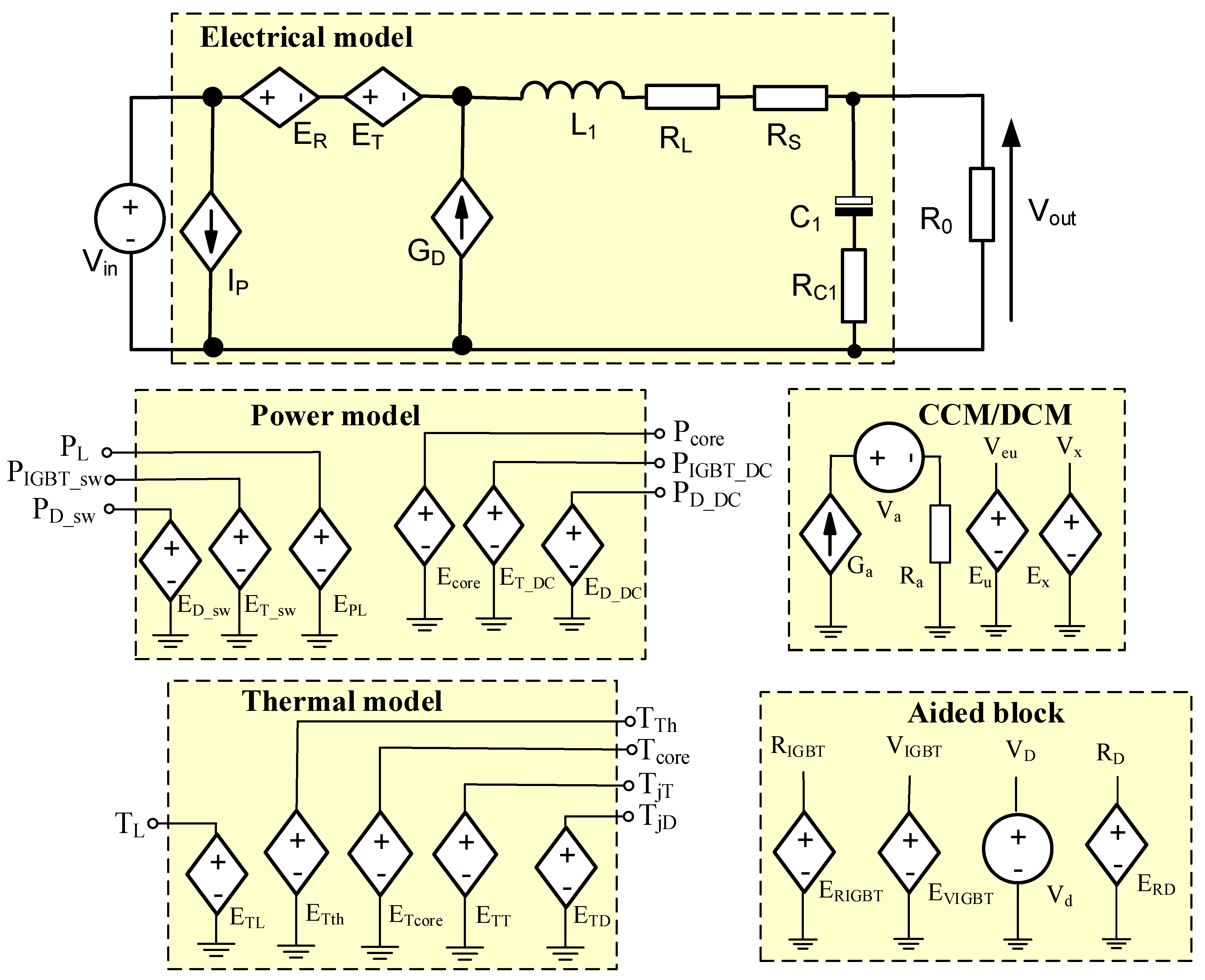
Figure 2.
All the voltages and currents in the considered network correspond to the average values of these quantities in the steady state. The converter under test is supplied from a voltage source Vin, and its load is a resistor R0. There are external components of the modeled converter.
The proposed model consists of three blocks: electrical model, power model and thermal model. In the electrical model, the controlled voltage sources E
T and E
R and the current source G
D represent the main circuit of the averaged diode–transistor switch. The concept for the formulation of this part of the model is described, e.g., in [
10]. This model is used to compute the average values of the diode current (current source G
D) and the IGBT voltage (voltage sources E
T and E
R) in the converter operating both in CCM (Continuous Conduction Mode) and DCM (Discontinuous Conduction Mode). These voltages and currents depend on the junction temperature T
jT of the transistor and temperature T
jD of the diode, respectively. The model uses piece-wise linear DC characteristics of the diode and the transistor. In the description of these characteristics, the linear dependences of the forward voltage and series resistance of these semiconductor devices on their junction temperature are used [
10].
The output voltage and current of the controlled sources used in the main circuit of the averaged diode–transistor switch are described as follows:
The values of parameters describing characteristics of the IGBT (VIGBT and RIGBT) and of the diode (VD and RD) are computed in the Aided block using the controlled voltage sources EViGBT, ERIGBT and ERD and a voltage source Vd. The dependence of the considered parameters on the junction temperature of these devices is considered.
The inductor L
1 and resistor R
L, representing the resistance of its winding, are connected in series. Resistance R
L depends linearly on the winding temperature T
L [
23]. Resistor R
C1 corresponds to the ESR of capacitor C
1.
The block denoted as CCM/DCM is used to detect the mode of operation of the analyzed DC-DC converter. The equivalent duty cycle of the control signal V
eu is computed in this block using a controlled voltage source E
eu. This parameter is used in descriptions of the output voltage of the voltage sources E
T and E
R, as well as of the output current of the current source G
D, according to the formulas given in [
10]. The value of V
eu is not lower than the actual duty cycle of the control signal d [
4,
5,
10]. The other elements occurring in the block CCM/DCM (controlled current source G
a, voltage source V
a, resistor R
a and controlled voltage source E
x) are used to compute voltage V
eu.
In addition to the components corresponding to the actual components of the modeled converter, the electrical model contains additional R
S and I
P components that represent additional loss components in the modeled DC-DC converter. The resistor R
S represents the parasitic resistance of the connections in the converter. The controlled current source I
P models an additional component of the converter input current resulting from switching losses in semiconductor devices and core losses in the inductor. The current of this source is given as follows:
where P
core—the power dissipated in the core; P
D_sw—the switching losses in the diode; and P
IGBT_sw—the switching losses in the transistor. All the mentioned components of power losses are computed in the power model.
The power model is used to compute conduction and switching power losses in the components of the tested DC-DC converter. The controlled voltage sources ED_sw, ET_sw and Ecore are used to compute switching power losses in the diode PD_sw, in the transistor PIGBT_sw and in the core Pcore, respectively. In turn, the controlled voltage sources ED_DC, ET_DC and EPL are used to compute conduction power losses in diode PD_DC, in transistor PIGBT_DC and in inductor PL, respectively.
In the thermal model, the junction temperatures TjD of the diode and TjT of the IGBT, as well as the temperature of the inductor winding TL, the inductor core Tcore, and the case of the IGBT module TTh, are computed using the controlled voltage sources ETD, ETT, ETL, ETcore and ETth, respectively. This model contains only the controlled voltage sources without any RC network, because the presented model is designated for use in DC analysis.
The module case temperature Tth and the junction temperatures of the diode T
jD and IGBT T
jT are calculated using the following formulas:
where T
a denotes the ambient temperature, R
thT is the thermal resistance of the IGBT, R
thD is the thermal resistance of the diode, and R
thm is the mutual thermal resistance between the thermocouple and the IGBT and between the thermocouple and the diode. In turn, P
D_DC and P
IGBT_DC denote the conduction power losses in the diode and the IGBT, whereas P
D_sw and P
IGBT_sw are the switching power losses in these devices.
The form of Equation (7) shows that the module case temperature Tth is higher than Ta only due to the power dissipated in the semiconductor devices included in the IGBT module.
Switching losses are described using the following equations:
where f
0 denotes the frequency value for which the values of parameters P
D_sw0 and P
IGBT_sw0 were determined, and I
Tav is the average value of the IGBT collector current, whereas α, α
fD, α
fT, α
IT and I
Tav0 are the model parameters.
Conduction power losses in semiconductor devices are described using the following formulas:
where I
Dav denotes the average value of the diode current. The values of I
Dav and I
Tav are calculated in the electrical model. The values of voltages V
D and V
IGBT and resistances R
D and R
IGBT are calculated in the Aided block, whereas voltage V
eu is computed in the block CCM/DCM.
The inductor winding temperature TL is the sum of three components: temperature Ta; the product of the thermal resistance of the winding and the power lost in the winding; and the product of the mutual thermal resistance between the core and winding Rthc-w and the power lost in the core Pcore. In turn, the core temperature Tcore is the sum of three components: temperature Ta; the product of the thermal resistance of the core Rthcore and the power Pcore; and the product of Rthc-w and the power lost in the winding PL.
The power P
L is calculated as the product of the square of the average value of the inductor current and the resistance of its winding R
L. In turn, power P
core is described as follows:
where k is a model parameter.
The values of the model parameters describing the electrical properties of the transistor and diode were determined based on the static characteristics of these devices published by the manufacturer or derived from the measurements performed by the user. The values of the VD and RD parameters were obtained from the approximation of the characteristics of the diode operating in forward mode, and the values of the VIGBT and RIGBT parameters from the approximation of the output characteristics of the transistor corresponding to a high value of the control voltage VGE. The inductance of inductor L1 and its series resistance RL were measured using an RLC bridge. The values of resistance RC1 and the capacitance C1 of the capacitor are determined in a similar manner.
The values of the thermal resistances of the transistor R
thT and diode R
thD and the mutual thermal resistance R
thm between these devices were measured using the indirect electrical method described in [
38]. In turn, the thermal resistances of the core R
thcore and the mutual thermal resistance between the core and the inductor winding R
thc-w were measured using the method described in [
22].
The values of the coefficients appearing in the description of individual power loss components in semiconductor devices and in the inductor core were determined based on the approximation of the measured characteristics of the tested DC-DC converter. The PD_sw0 coefficient is determined for a selected value of the converter operating frequency f0 based on the measured value of the diode junction temperature and the ambient temperature at known values of PD_DC power and thermal resistance of this device. The αfD coefficient is calculated based on the measured values of PD_sw power for two values of frequency f.
The value of the coefficient PIGBT_sw0 is determined for a selected frequency value f0 and the average value of the transistor current ITav0 based on the measured value of the transistor junction temperature and the ambient temperature at known values of PIGBT_DC power and thermal resistance of this device. Based on the measured values of PIGBT_sw power for two values of frequency f and two values of transistor current ITav, values of the coefficients α, αTf and αIT are determined. The value of the coefficient k is determined based on the measured value of the inductor core temperature Tcore at a fixed temperature value Ta and fixed values of the frequency f and the duty cycle d of the control signal and the supply voltage of converter Vin.
4. Results
Through the use of the buck converter model presented in the previous section, a series of simulations of the considered converter was performed. The influence of supply voltage, load resistance and parameters of the control signal on the converter characteristics was considered. Then, simulations in identical conditions were performed in PLECS software using the model of the IGBT module proposed by its creator [
40] and the models of the capacitor and the inductor containing their series resistances. The thermal model of the module was extended by the elements responsible for heat transport from the case to the ambient environment. In the case of the inductor, core losses were omitted, because the parameters describing its B(H) dependence are out of the range formally acceptable by PLECS. The magnetic force in saturation cannot be higher than the product of the coercive magnetic force and the number 20. For the used ferromagnetic core, the value of the coercive magnetic force is 50 A/m, whereas the saturation magnetic force amounts to 4 kA/m.
It is worth noting that PLECS makes it possible to model the nonlinearity of the magnetization curve, but it is impossible to take into account the influence of the core losses on the characteristics of the tested switched-mode power converters in a simple manner [
41]. As described in [
42], the possibility of building complex magnetic components in a special magnetic circuit domain based on the permeance–capacitance analogy was not explored in this paper.
The steady-state results of these simulations are shown in the figures below. In each of these figures, the solid lines denote the simulation results obtained using the averaged electrothermal model and DC analysis, and the dashed lines represent the simulation results obtained using PLECS software, whereas the points indicate the measurement results.
Section 4.1 includes characteristics showing the influence of the control signal parameters and load resistance on the converter output voltage, energy efficiency and temperature of selected components of the tested converter.
Section 4.2 presents the calculated dependences of the components of power losses in the converter components on the output current and frequency. In
Section 4.3, the distribution of power losses in the tested converter in selected operating conditions is analyzed.
4.1. Characteristics of the Buck Converter
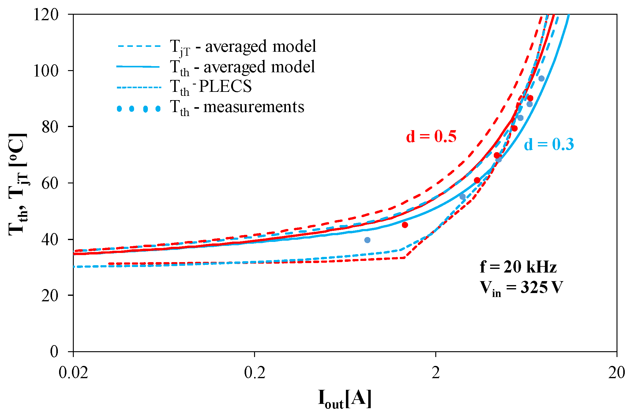
Figure 3,
Figure 4,
Figure 5 and
Figure 6 present the results of the tests carried out at the input voltage V
in = 325 V and the control signal frequency f = 20 kHz. These tests were carried out in a wide range of load current I
out changes at selected values of the control signal duty cycle d.
Figure 3 illustrates the influence of the duty cycle d on the output characteristics of the considered converter.
Figure 3 shows that the proposed model provides a good match between the calculations performed using SPICE and PLECS and the measurement results. The discrepancies between the results of measurement and computations do not exceed 2% for the proposed model and 8% for the PLECS model. An increase in the d coefficient value causes an increase in the output voltage V
out of the tested converter. For the used values of load current I
out, the tested converter operates in both CCM and DCM. The critical current below which the converter operates in DCM is about 1 A and decreases with an increase in the parameter d. For high I
out current values, a drop in the V
out voltage value is visible. This is caused by voltage drops on the converter components.
Figure 4 presents the dependence of the temperature of the IGBT module (solid lines) and the junction temperature of the transistor included in this module (dashed lines) on current I
out.
The junction and case temperatures of the considered IGBT module increase with an increase in the coefficient d. The values of TjT are higher than the values of TTh for all considered converter operating conditions. The values of temperature Tth obtained with the PLECS computations are underestimated by some Celsius degrees for low values of Iout and overestimated for high values of this current. The values of temperature Tth obtained using the averaged model differ from the measurement results by no more than 5 °C. The values of parameter d weakly influence the values of temperature Tth.
Figure 5 shows the inductor core temperature T
core as a function of current I
out. The results of computations performed in PLECS software are not presented in this figure, because the thermal properties of the inductor core were not included in the available model of this device.
The presented curves show that at low values of I
out current, the core temperature does not depend on the value of this current, because the main reason for the increase in the core temperature is a hysteresis loss proportional to the converter input voltage of 325 V. The curves T
core(I
out) obtained for d = 0.3 and d = 0.7 overlap. The influence of the d factor value on T
core temperature is visible in this operating range. For higher values of I
out current, an increase in the T
core temperature value is visible as a function of this current. This is caused by an increase in losses in the inductor winding and mutual thermal couplings between the winding and the inductor core [
22].
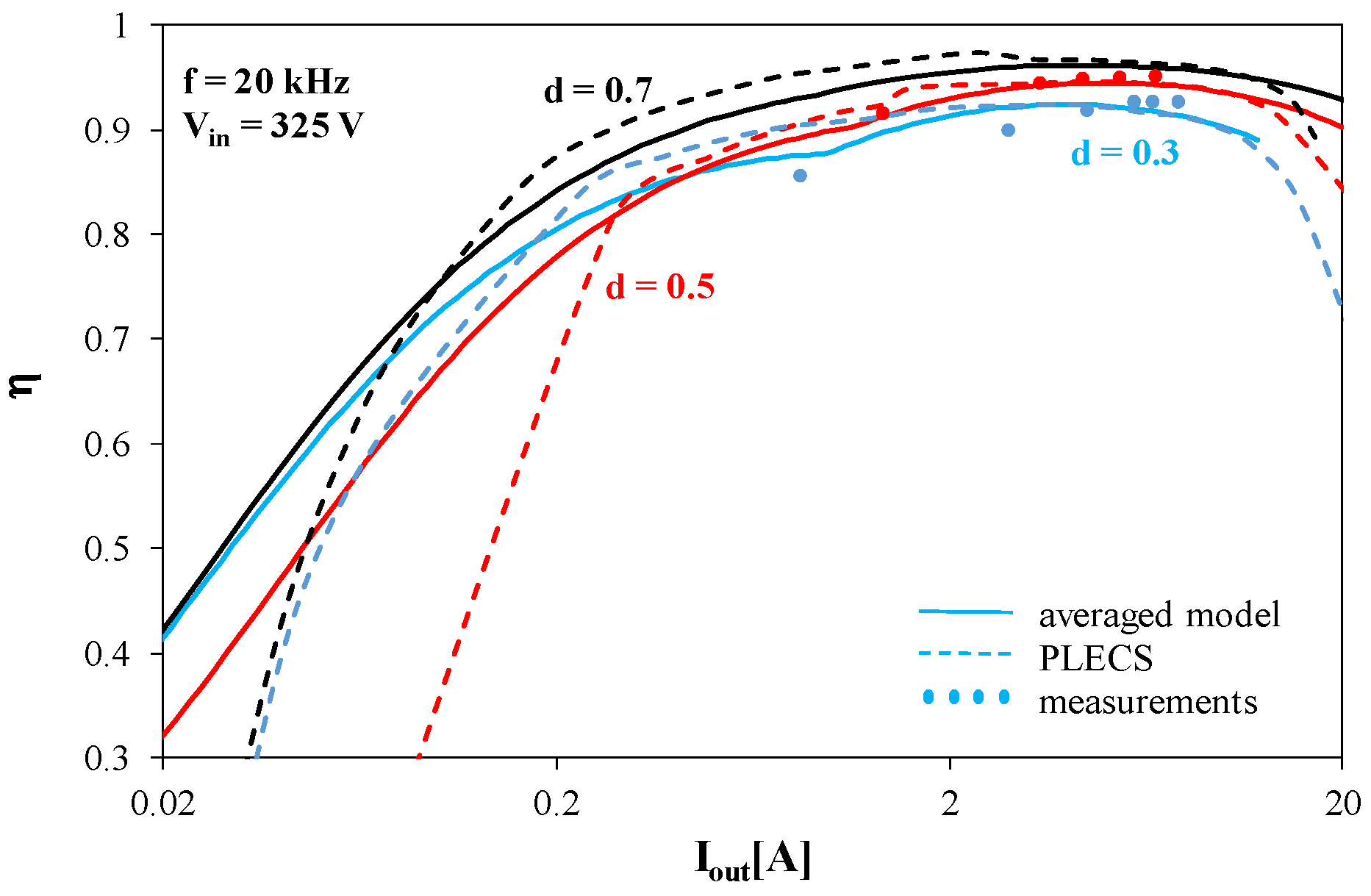
Figure 6 illustrates the influence of current I
out on the energy efficiency η of the converter. For the computations performed using SPICE software and for the measurements, the value of η is calculated as the quotient of the power dissipated in the load and the power taken from the power supply. In contrast, due to the specific operation of PLECS, in which each component of the losses is calculated separately and used only to compute the device junction temperature, the other manner of calculation of η is used. These calculations were performed using the following formula:
where P
inavg denotes the average value of the input power of the tested DC-DC converter, whereas ΣP
loss denotes the sum of average values of the power losses in the converter components. The sum contains conduction and switching losses in the diode and in the transistor, as well as the power losses in the inductor winding and the core. The core losses are calculated using Formula (12).
The dependences η(Iout) obtained using the measurements and computations have maximums at Iout equal to about 6 A. The value of this maximum increases when the coefficient d increases and reaches as much as 96% at d = 0.7. The decrease in energy efficiency in the range of high currents is related to an increase in losses in semiconductor devices. The dependences η(Iout) obtained using PLECS software are consistent with the measurement results only for high values of the output current, whereas in the range of low values of Iout, the calculated values of energy efficiency are underestimated. The obtained results suggest that the model of the tested DC-DC converter implemented in PLECS software describes the power losses in a simplified form. In contrast, the results obtained using the considered averaged model fit well with the measurement results.
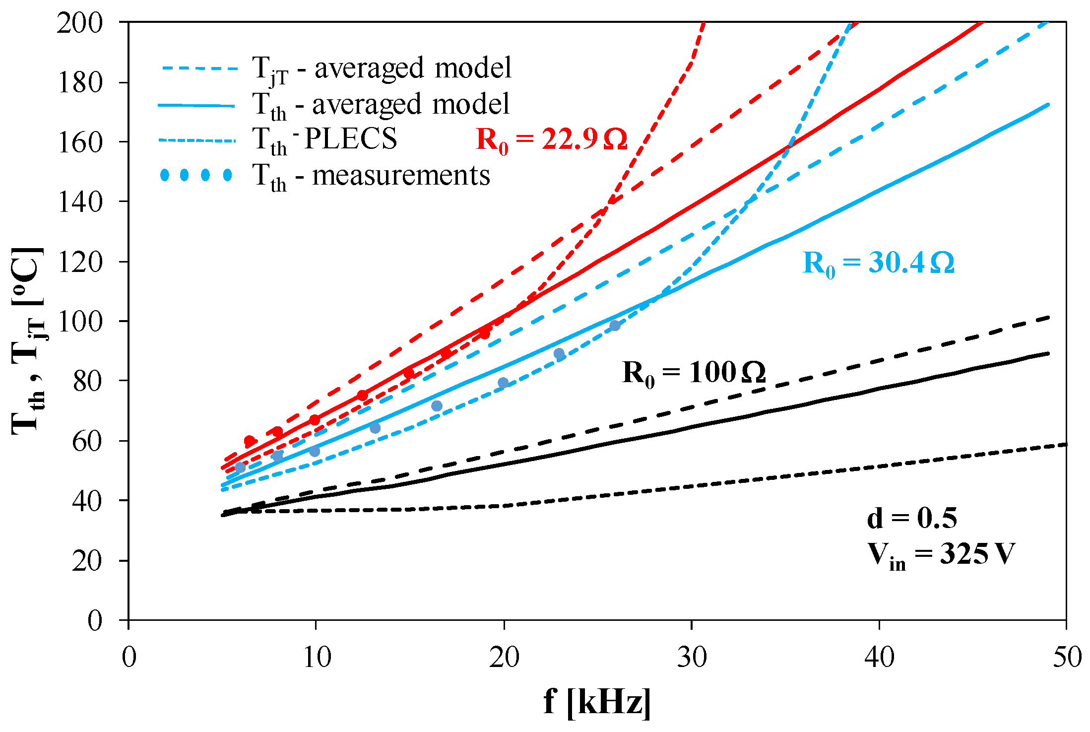
Figure 7,
Figure 8,
Figure 9 and
Figure 10 present the results of the tests carried out at the input voltage V
in = 325 V and the control signal duty cycle d = 0.5. These tests were performed for different values of switching frequency f at selected values of load resistance R
0.
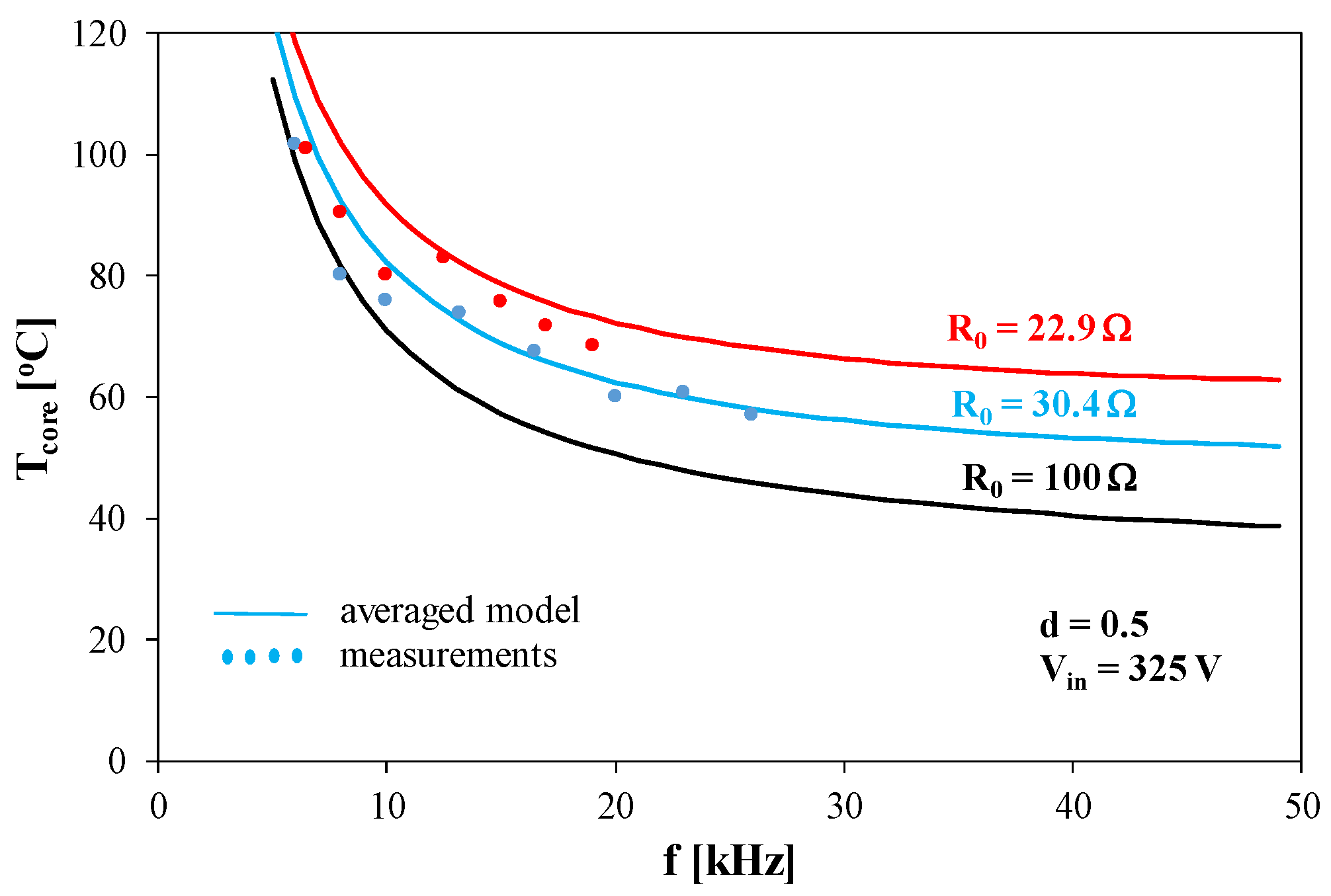
Figure 7 shows the dependence of the IGBT module temperature and the transistor junction temperature on frequency.
As can be seen, both temperatures considered increase as a function of frequency and decrease as a function of load resistance R0. Similarly, the difference between temperatures TjT and TTh increases with increasing switching frequency, even reaching 20 °C. It is worth noting that with an identical value of load resistance, the temperature value of the IGBT module increases by as much as 120 °C when changing the frequency from 5 to 40 kHz. Of course, the increase in Tth due to an increase in frequency decreases with an increase in R0. For high values of frequency, the results of calculations performed using PLECS software are overestimated in comparison with the results obtained using SPICE software, even by 100 °C.
Figure 8 shows the effect of frequency on the inductor core temperature.
With an increase in frequency, the inductor core temperature decreases monotonically. It is worth noting that a change in the load resistance value in the considered range results in only a small change in the Tcore temperature value, visible especially in the higher-frequency range. The presented characteristics cannot be obtained using PLECS software because the properties of the inductor core in this software are omitted.
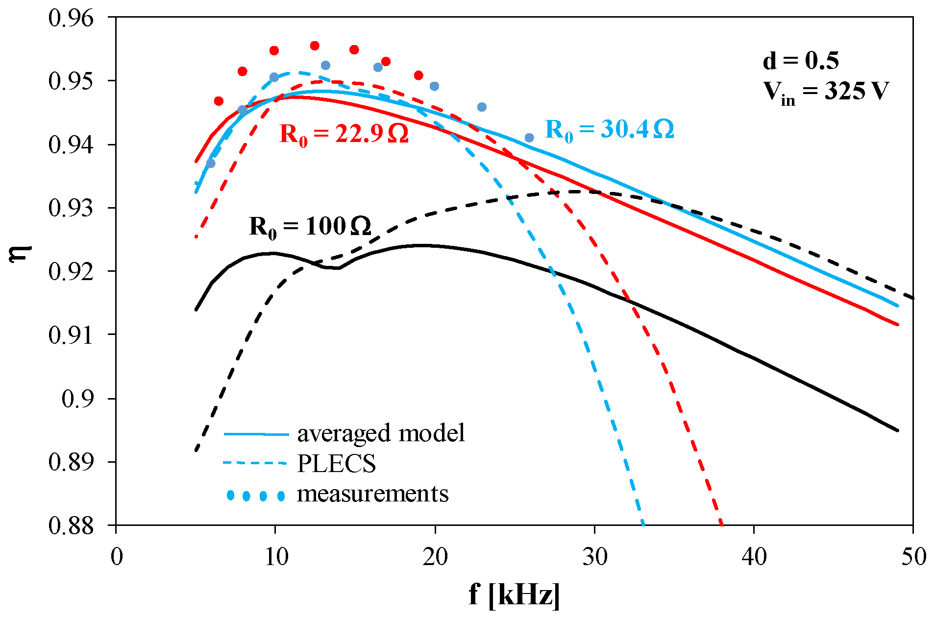
Figure 9 presents the dependence of the energy efficiency of the considered converter on frequency.
The dependences η(f) obtained from the measurements and calculations have a maximum. With an increase in resistance R0, the frequency at which this maximum is observed increases. The value of energy efficiency increases for lower values of resistance R0. The efficiency rapidly decreases in the range of low frequency due to the DCM operation of the tested converter. The considered dependences obtained using PLECS software show a fast decrease in the range of high frequency and low load resistance. The obtained results suggest that the switching losses in semiconductor devices are overestimated.
Analyses were also carried out to illustrate the influence of the input voltage on the temperatures of individual components of the converter under consideration, its energy efficiency and the power lost in these components. The results of these considerations are presented in
Figure 10,
Figure 11 and
Figure 12. The calculations were carried out for selected values of frequency f, with d = 0.5 and R
0 = 25 Ω.
Figure 10 shows the dependence of the IGBT module temperature Tth and temperature T
jT on V
in voltage.
Both temperature TjT and temperature TTh increase as a function of voltage Vin. The changes in the values of these temperatures with an increase in voltage Vin in the considered range are the biggest for the highest of the considered converter switching frequencies. In these conditions, they even exceed 100 °C. The values of temperature Tth obtained using PLECS show much greater changes than the values of this temperature obtained using the proposed averaged model implemented in SPICE. The differences between the results obtained using both the considered models even exceed 100 °C.
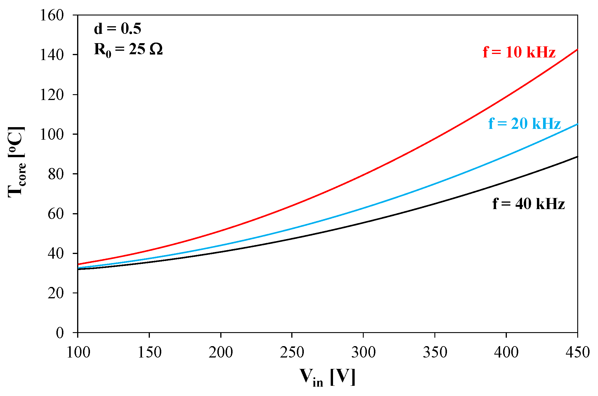
Figure 11 shows the effect of frequency on the dependence of the core temperature on the input voltage.
The obtained Tcore(Vin) dependencies are increasing functions. An increase in frequency results in a decrease in Tcore. For the lowest of the considered frequency values, the change in the core temperature value with changes in Vin voltage in the considered range exceeds as much as 100 °C. This means that in order to limit the core temperature, it is advantageous to set a higher value of the converter operating frequency.
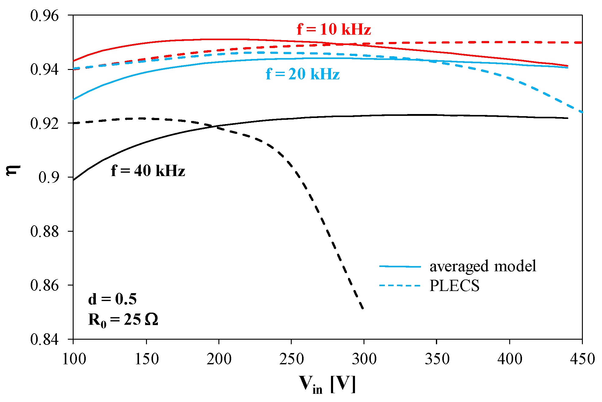
Figure 12 presents the dependence of the energy efficiency of the considered converter on the input voltage for selected values of frequency.
It can be seen in
Figure 12 that for each of the considered switching frequency values, one can find the voltage value V
in for which the dependence η(V
in) takes the highest value. According to the results obtained using SPICE, this optimal voltage value V
in increases with increasing frequency. In contrast, the dependence η(V
in) obtained using PLECS shows the opposite tendency, because this software overestimates the switching losses in semiconductor devices.
The results of the investigations presented in this section show that the proposed averaged electrothermal model of a buck converter makes it possible to obtain good accuracy in modeling characteristics that describe the electrical and thermal properties of this converter. Therefore, this model is used in the subsequent portion of this article to analyze the distribution of power losses between semiconductor and magnetic components of this DC-DC converter.
4.2. Dependence of the Components of Power Losses on Operating Conditions
On the basis of the electrothermal DC analyses of the tested DC-DC converter performed using the averaged electrothermal model of this converter, the components of power losses were computed. The dependences of these power losses on the converter operating conditions are presented in this subsection. All presented results of computations correspond to the steady state.
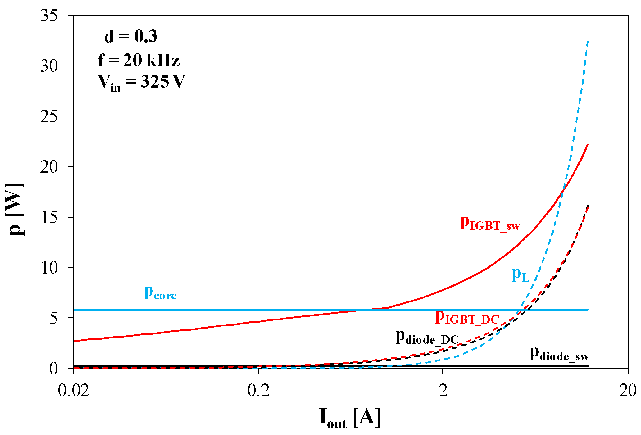
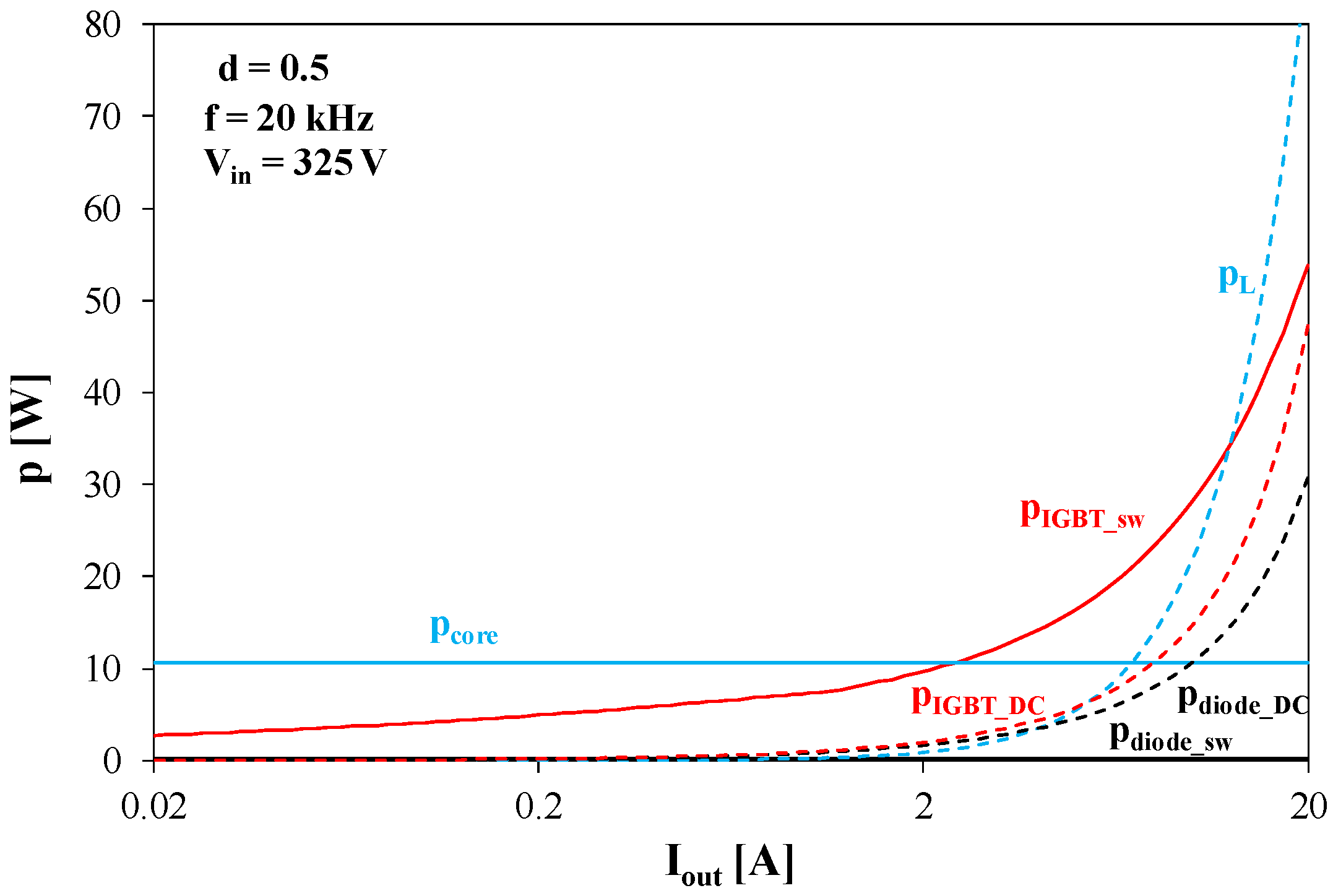
In all the figures in this subsection, the solid lines denote the loss components related to switching, and the dashed lines indicate the loss components related to conduction. The particular loss components are marked with the following symbols: PL—inductor winding losses; Pcore—inductor core losses; PD_DC—diode conduction losses; PIGBT_DC—transistor conduction losses; PD_sw—diode switching losses; and PIGBT_sw—transistor switching losses.
Figure 13 and
Figure 14 present the influence of current I
out on the above-mentioned components of power losses. The results shown in
Figure 13 correspond to d = 0.3, whereas the results presented in
Figure 14 correspond to d = 0.5. The computations were performed for f = 20 kHz.
Through an analysis of the graphs presented in
Figure 13 and
Figure 14, it can be seen that the switching losses, P
D_sw, of the diode are much lower than the other loss components. The losses P
core in the core have a fixed value over the entire range of I
out current changes, and their value is higher for a higher value of the d coefficient. In the range of low I
out current values, the core losses are the dominant component of the losses in the tested converter. The conduction losses P
D_DC of the diode and P
IGBT_DC of the transistor, as well as the losses in the inductor winding P
L, increase with an increase in I
out current. It is worth noting that the conduction losses in the diode and the transistor have similar values. The switching losses P
IGBT_sw in the transistor increase as a function of I
out current and at I
out values exceeding several amps are the dominant component of the losses in the converter. Through a comparison of the results presented in
Figure 13 and
Figure 14, it can be seen that an increase in the value of the duty cycle d causes a significant increase in the value of all the loss components and, in particular, an increase in the share of losses in the inductor winding and conduction losses of semiconductor devices in the total losses in the converter.
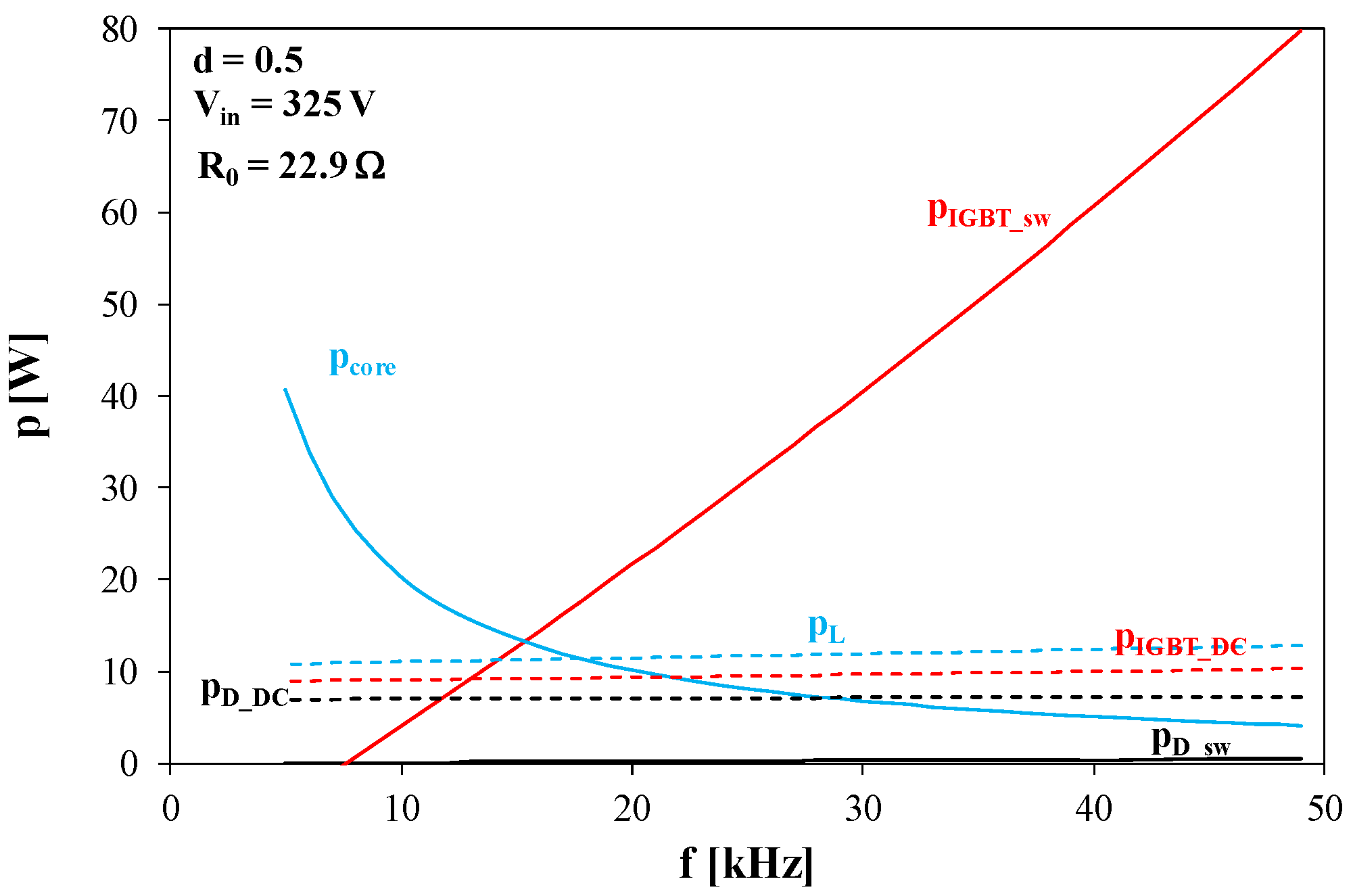
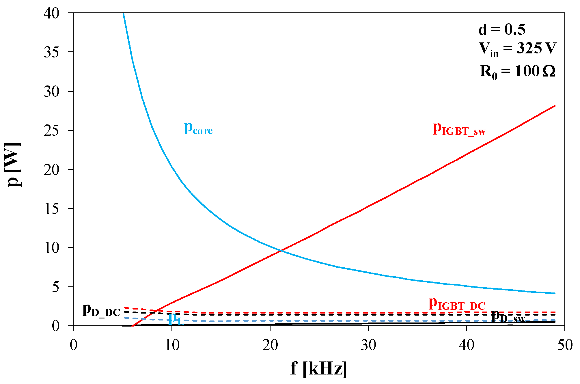
Figure 15 and
Figure 16 present the influence of f on the considered components of power losses. The results presented in
Figure 15 refer to the operation of the converter with load resistance R
0 = 22.9 Ω, whereas the results in
Figure 16 refer to operation at R
0 = 100 Ω.
In both the figures, it can be seen that the dominant components of power losses are Pcore and PIGBT_sw. The power Pcore decreases as a function of f, and its value practically does not depend on the value of R0. In turn, the power PIGBT_sw linearly increases as a function of frequency, and an increase in the value of R0 results in a decrease in the nominal value of PIGBT_sw. The conduction losses of semiconductor devices and the losses in the inductor winding PL practically do not change as a function of frequency, but their values decrease with an increase in resistance R0. Switching losses in the diode are at a negligible level.
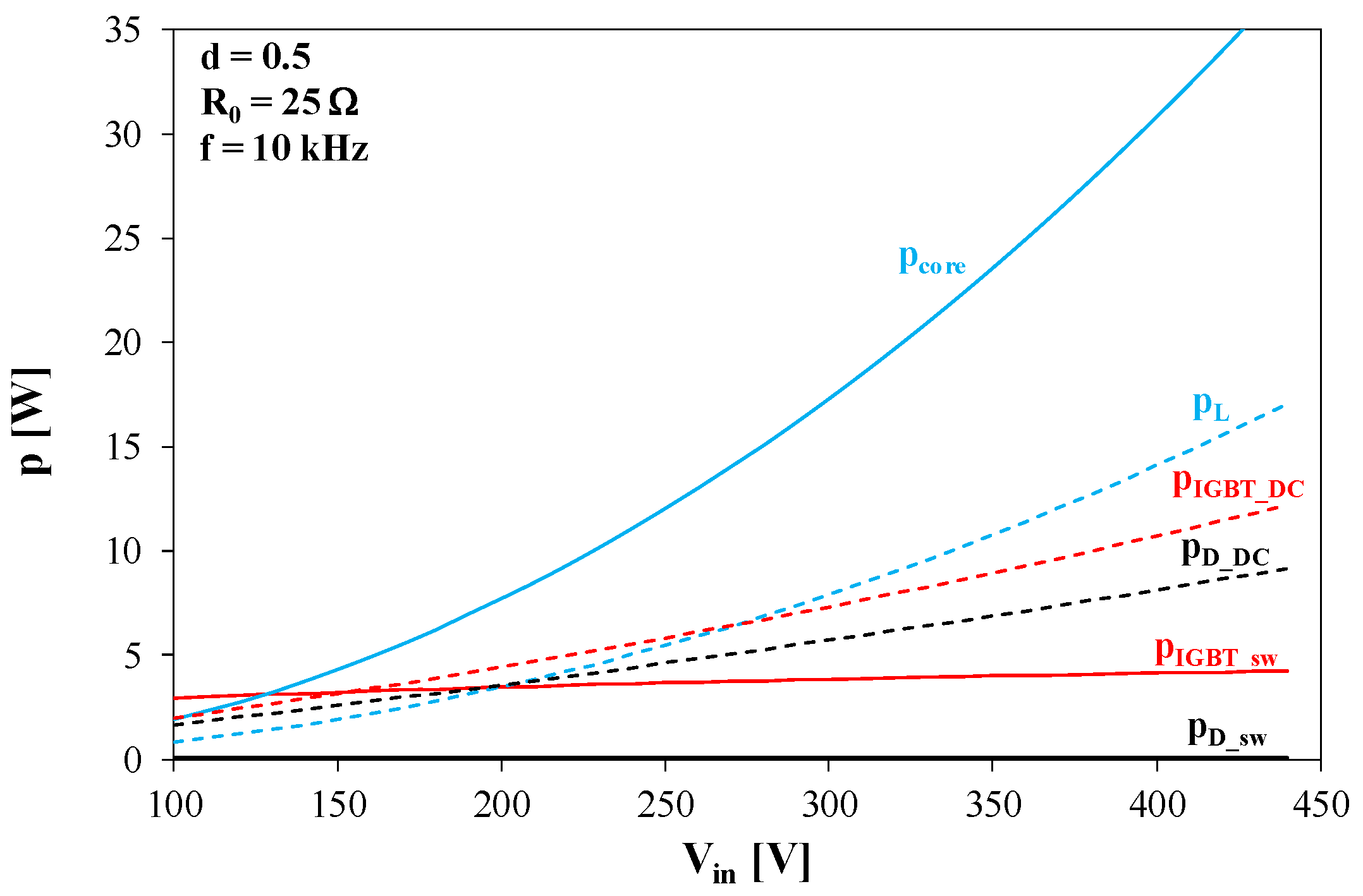
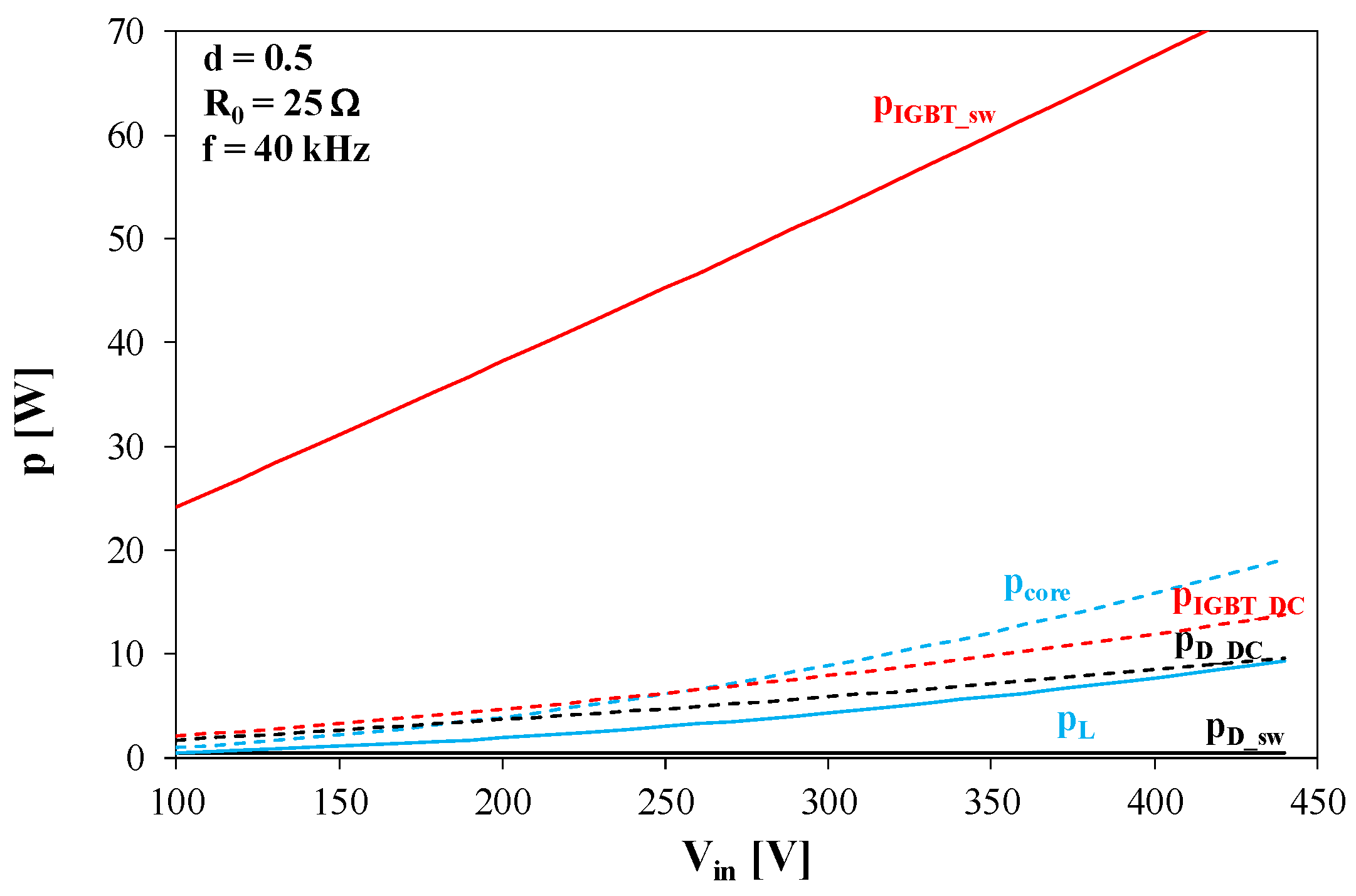
The influence of V
in voltage on the components of power losses is shown in
Figure 17 for frequency f = 10 kHz and in
Figure 18 for frequency f = 40 kHz.
In
Figure 17 and
Figure 18, it is shown that an increase in V
in voltage causes an increase in all the components of power losses. At the lowest of the considered switching frequencies, the dominant component of the power losses is P
core, while for the highest of these frequencies, the dominant component is the switching losses of the transistor. The remaining components of the losses do not change significantly with the changes in frequency. The presented dependences indicate that the supply voltage is a factor that significantly affects the power losses in the individual components of the converter, and this affects its energy efficiency.
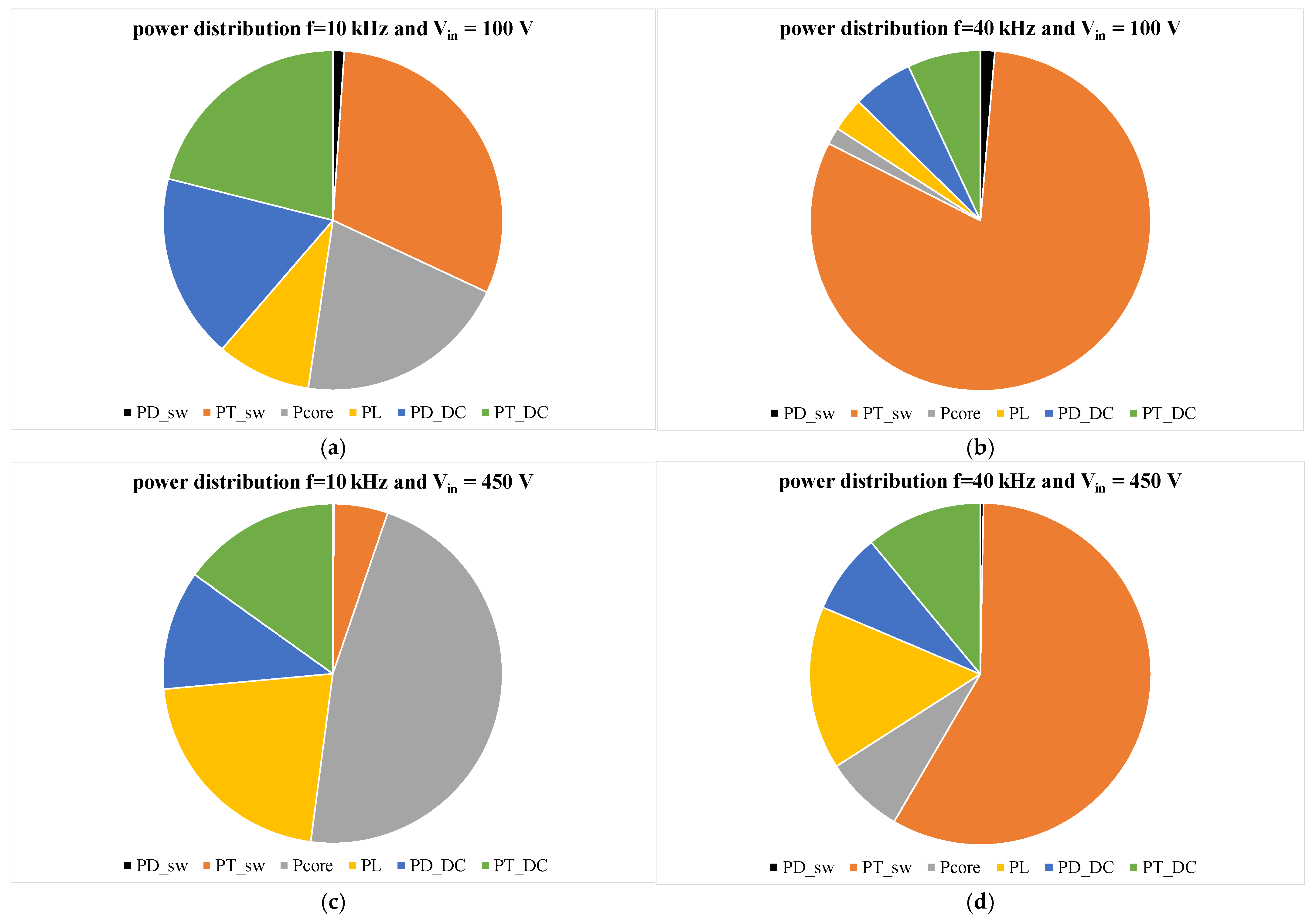
4.3. Power Loss Distribution at Selected Operating Conditions
To illustrate the influence of the operating point on the participation of each component of the power losses in the total power losses in the tested buck converter, the pie diagrams shown below were created.
Figure 19 shows the distribution of power losses in the tested buck converter operating at different values of V
in and f. The presented results were obtained at load resistance R
0 = 15 Ω and d = 0.5.
As can be seen, the distribution of losses in particular converter components changes with a change in the frequency and input voltage. In each of the considered cases, switching losses in the diode are negligible. At a low value of V
in voltage and low frequency (
Figure 19a), the most important losses are the transistor switching losses, but the conduction losses of semiconductor devices and the losses in the inductor core together constitute over 60% of the total losses in the converter. With an increase in f (
Figure 19b), the transistor switching losses constitute over 80% of all the losses in the converter. At a high value of V
in, at low values of f (
Figure 19c), almost half of the losses in the converter are P
core power, while at a high switching frequency (
Figure 19d), less than a half of the losses are P
T_sw power.
Through a comparison of the results presented in
Figure 19, it can be concluded that in the analyzed DC-DC converter operating at high frequency, switching losses in the transistor dominate. At low frequencies, P
core values are of significant importance. An increase in the input voltage value results in an increase in I
out, which translates into an increase in the share of conduction losses in the semiconductor devices and in the inductor.
5. Conclusions
This paper proposes the use of an averaged electrothermal model of a buck converter in calculations of power losses in the components of this converter. The use of this model allows the determination of the characteristics of the DC-DC converter under consideration, taking into account self-heating and mutual thermal couplings between the dies in the IGBT module. It was shown that these characteristics are consistent with the characteristics obtained from the measurements. The characteristics computed using PLECS software, presented for comparison, show that this software makes it possible to properly compute the values of the tested converter output voltage and the temperature of the module; however, the models of the inductors used in this software are too simple. Therefore, the power losses and η of the tested converter should be calculated taking into account the proposed description of the core losses.
The main advantages of the proposed averaged electrothermal model are high accuracy and short computation time. Through the use of this model, the characteristics of the tested converter can be obtained using fast DC analysis. The use of PLECS necessitates transient analysis, which makes it possible to obtain only coordinates of one point in the characteristics after each analysis. This means that the use of the proposed averaged model makes it possible to obtain more accurate results in a shorter time period than PLECS software.
In the previous sections, the results of the research illustrating the influence of selected factors on power losses in individual components of the buck converter were presented. The analyses carried out showed that in different operating conditions of the DC-DC converter under consideration, different loss components determine its energy efficiency. For example, for fixed values of frequency and input voltage and low load current values, the greatest power losses occur in the inductor core, while for high values of this current, the IGBT transistor switching losses and semiconductor device conduction losses dominate, which increase as a function of this current. In turn, for a fixed value of load resistance, losses in the inductor core decrease as a function of frequency, and the transistor switching losses increase as a function of frequency. The remaining loss components practically do not depend on frequency. The value of the converter input voltage is also of significant importance. All the power loss components increase with an increase in this voltage.
It is also worth noting that the presented method of analyzing the properties of the considered class of DC-DC converters allows for a very simple determination of the converter operating conditions (frequency, input voltage, load current) at which there will be no risk of excessive temperature increase in individual components of the converter and at which it will be possible to obtain an acceptable value of energy efficiency. The short time duration of simulations, counted in single milliseconds, is also important. It ensures high calculation efficiency.
The presented results and analysis method may be useful for designers of switched-mode power converters. They can also be a tool with which to analyze the influence of selected factors on the properties of such a system and other DC-DC converters. Through the use of the proposed averaged electrothermal model of a buck converter, it is possible to rapidly select a device, the properties of which significantly limit its energy efficiency.


