Abstract
This paper proposes a flattened power electronic design approach to enhance both power density and thermal management performance. As essential components in electrified energy conversion, evaluations of power converters are strongly based on their power density. Achieving a compact design typically requires a well-optimized printed circuit board (PCB) layout, optimal component design and selection, and an efficient thermal management system. During high-power operation, significant power losses can lead to substantial heat generation. Without effective thermal mitigation, this heat buildup may result in excessive temperature rises or even system failure. To address this challenge, this paper developed a flattened power converter design methodology to increase the effective heat-dissipation area without expanding the total volume consumption. This proposed design improves thermal performance and, in turn, enhances overall power density. A three-phase inverter prototype is developed and tested to demonstrate the effectiveness of the proposed method.
1. Introduction
The increasing global demand for efficient and sustainable energy solutions has accelerated advancements in power electronics, especially within energy conversion applications such as renewable energy systems, electric vehicles, and grid integration. At the core of these applications lie power converters, which are essential for enabling reliable, efficient, and adaptable energy conversion. However, optimizing the design and performance of power converters involves navigating a complex interplay of factors, with power density and thermal management emerging as two of the most critical and challenging performance metrics.
Power density, defined as the ratio of power delivered to the physical volume of the system, plays an important role as a performance indicator in power converter design [,,,]. High power density signifies a converter’s ability to deliver substantial power within a compact physical footprint, which is particularly advantageous in space-constrained applications such as electric vehicles, portable electronics, and compact renewable energy systems. Achieving such high power density presents multiple engineering challenges, including the need for component miniaturization, optimized circuit layout, and robust thermal management. This is often facilitated by the integration of advanced semiconductor technologies, particularly wide-bandgap (WBG) materials such as silicon carbide (SiC) and gallium nitride (GaN), which support higher switching frequencies and lower conduction and switching losses. Furthermore, the adoption of multi-layered printed circuit boards (PCBs), advanced packaging methodologies, and high-frequency magnetic components plays a crucial role in reducing system size and enhancing power density. Nevertheless, the resulting increase in thermal stress underscores the importance of a highly effective thermal management strategy to ensure system reliability and longevity.
Thermal management is a critical consideration in power electronics, as excessive heat generated during operation can significantly degrade the performance, reliability, and lifespan of power converters. The primary sources of heat include conduction losses in power semiconductor devices, switching losses during rapid transitions, and magnetic losses within inductive and transformer components [,,,]. As the trend toward higher power density continues, the challenge of effectively dissipating this heat becomes more pronounced. Conventional thermal management approaches—such as the use of heat sinks, forced air cooling, liquid cooling, and thermal interface materials (TIMs)—are commonly employed to transfer heat away from thermally sensitive components. However, in high-power-density designs, these traditional methods often encounter limitations due to the restricted space for thermal components. Moreover, non-uniform heat distribution can result in localized hotspots, which exacerbate thermal stress and increase the risk of component degradation or failure. Also, in [,,,], research about thermal and multi-physics simulation is included, which shows that an increased footprint always means a better thermal dissipation performance. By redistributing components across a planar geometry, the design facilitates more uniform thermal conduction paths and enhances natural or forced convection across the surface. The flattened layout, therefore, aligns with established thermal principles while providing a practical path toward compact yet thermally efficient power electronics systems.
The trade-off between power density and thermal management poses a significant challenge in power converter design. As power density increases, so does the rate of heat generation per unit volume, which can lead to thermal bottlenecks, reduced system efficiency, and compromised reliability. Effective thermal management is therefore essential to mitigate these adverse effects and to ensure stable operation across a range of load conditions [,,,]. Conversely, advances in thermal management can facilitate higher power densities by enabling more compact system designs without sacrificing performance or longevity. To address this interdependent challenge, innovative design strategies are needed to enhance both power density and thermal dissipation capabilities. One such strategy is the flattened power electronic design approach, which involves reconfiguring the geometry and layout of power converters to improve heat dissipation without increasing the converter’s overall volume [,,,]. This method increases the effective surface area available for heat dissipation and optimizes thermal conduction paths, thereby enabling better thermal regulation during high-power operation. The proposed design is particularly well-suited for grid-connected inverter systems, which serve as interfaces between distributed energy resources and the utility grid, as illustrated in Figure 1 [,,,,,,]. In solar energy applications, for instance, the generated DC power must be converted into AC power using a three-phase inverter before it can be integrated into the utility grid, as depicted in Figure 2.
Recent developments in flat and compact design methodology and multi-chip embedded power modules further reflect the industry-wide push toward flattened geometries for both thermal and volumetric efficiency. In [], a compact design methodology for a lumped-element capacitive-coupled-resonator filter was presented, and footprint size could be reduced by 40%. In [], a compact inductor integration method is presented, in which the partially overlapping magnetic structures result in a significantly reduced layout area, while introducing minimal parasitic coupling and preserving the functional integrity of each inductor.
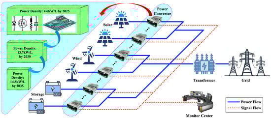
Figure 1.
The diagram of the grid-connected inverters to interface different energy resources with the roadmap of power density requirement [].
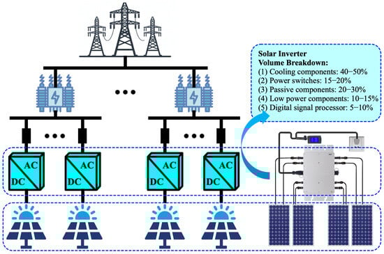
Figure 2.
Structure and volume breakdown of grid-connected solar inverters.
This paper introduces the concept of flattened power electronics as a novel design methodology to optimize thermal management and improve power density. By rethinking the physical layout and choice of electronics, and integrating advanced thermal management solutions, the proposed method aims to enhance heat dissipation while maintaining or reducing the overall footprint of the power converter. A three-phase inverter is used as a case study to demonstrate the effectiveness of this approach, highlighting its potential for widespread application in energy conversion systems. The ultimate goal is to design a high-power-density facilities with high heat dissipation without an additional active cooling system.
2. Flattened Power Converter Design Methodology
The thermal management system is a critical component for addressing heat generation during power converter operation. In conventional designs, thermal management hardware often occupies a substantial portion of the converter’s overall volume. Because a specific amount of power loss must be dissipated into the surrounding environment to maintain acceptable operating temperatures, a sufficient surface area is essential to enable effective cooling. Under a fixed volume constraint, a flattened structural design can provide a significantly larger surface area for heat dissipation compared to a conventional cubic configuration. Figure 3 illustrates a comparison of surface areas between cubic and flattened block designs. Furthermore, the relationship between block dimensions (length, width) and surface area while maintaining a constant volume is presented in Figure 4. The results show that a flattened power converter design can achieve a surface area enlargement of more than 2–3 times compared to a cubic design. Consequently, this approach enhances the heat dissipation capability without incurring additional cost or significantly increasing the spatial footprint of the thermal management system.
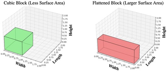
Figure 3.
Comparison of the surface area between the cubic and flattened shape of the block design.
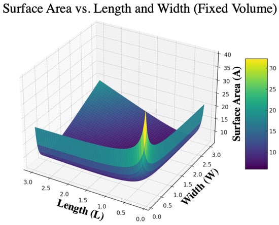
Figure 4.
Relation beteween the block length, width, and the surface area under the same volume.
For the analytical modeling of the thermal performance, especially when based on conduction, and the relation between the heat flow and the temperature difference, can be determined via the following equation:
where is the power of the heat energy flowing from one end to another, is the thermal conductivity of the conductive material, is the area perpendicular to the heat direction, and are the temperatures at the source and end, respectively. Based on the theoretical analysis, Finite Element Method (FEM) analysis is implemented in ANSYS (ANSYS Electronics Desktop 2025 R1) to verify the feasibility of the flattened power converter design. As shown in Figure 5, three-phase power switching chips were placed on the PCB with a flattened layout. Each chip was configured with 10–20 W of the heat source for emulation. It was demonstrated that the temperature rise is lower than 90 °C.
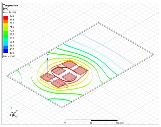
Figure 5.
Thermal performance of the flattened power converter design with temperature distribution.
For the analytical model-based optimal design, several procedures were developed including the following four steps: (a) determine the rated power of the converter, , and the energy conversion efficiency, ; (b) calculate the power loss of =; (c) configure the required upper limit of the conduction component temperature, the ambient temperature, conduction area, and component thermal conductivity; (d) initiate the width of the PCB to be twice that of the power chip area; (e) estimate the needed length of the board by taking the power switching chips as an integrated heat source, neglecting the vertical heat conduction of the PCB, and assuming the heat flow is conducted horizontally based on Equation (1); (f) iterate the different combinations of PCB width and length with the ANSYS for the optimal flattened power converter design, starting from step (e), reducing the length and increasing the width with a fixed value in each iteration.
Parasitic inductances, especially those associated with PCB traces and power loop layout, have a significant impact on the thermal performance of high-frequency power converters. Increased parasitic inductance can cause substantial voltage overshoot during device turn-off and slow down the effective switching speed, leading to higher switching losses and localized heating. These losses directly contribute to the increase in junction temperature and thermal stress in semiconductor devices. To mitigate these effects, the layout of the proposed flattened converter was optimized to minimize loop inductance by closely coupling the high-side and low-side switches, shortening trace lengths, and using wide copper planes. This not only reduces EMI but also improves thermal behavior by limiting energy dissipation in unwanted parasitics. The importance of parasitic inductance in determining junction temperature and system-level thermal reliability is further discussed in [,,].
For most of the controllers and converters, in order to embed the active cooling system, like fans, heat pipes, and water pumps, into the controllers and converters, engineers always prefer to design the converter as a cubic model. Moreover, since most of the other components are a cubic shape, like the motor, gear box, and battery system, this converter and controller design seems to be reasonable, as shown in Figure 3. However, as a result of the cubic design, higher dissipation power will be required to cool the converter. Then, the overall volume of converter will increase and the power density will further decrease. Therefore, the flattened power electronics model and designing methodology is necessary to satisfy the increasing thermal and power density requirements of current power electronics.
As shown in Figure 6, the three-phase inverter is responsible for the energy conversion between the DC solar panel and the AC grid utility. It includes three arms, each composed of two power switches: the upper switch and the lower one. Both of the switches operate complementarily to avoid short-circuit issues. Figure 7 demonstrates the flattened power electronic design structure and layout. The three-phase switching legs are configured in the middle of the PCB. In each phase leg, the upper and lower switches are placed in parallel. The three-phase switching legs are configured as a 2 by 3 matrix. The peripheral components of the PCB are configured with the filtering systems, including the output capacitors and inductors. Also, the digital signal controller is placed on one edge of the PCB to receive the voltage and current sampling information and send the switching signals for the purpose of controlling the turn-on and turn-off of the three-phase inverter power switches.
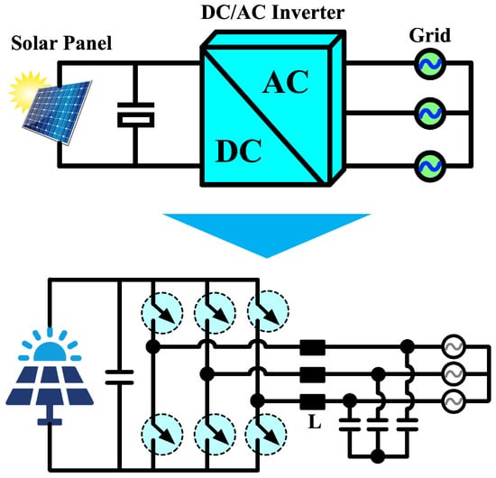
Figure 6.
Topology of a three-phase grid-connected solar inverter.
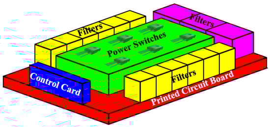
Figure 7.
Structure and layout of the flattened three-phase power converter.
In this way, the power converter system is flattened instead of a cubic block shape. The total area of surface can be enlarged by 3–5 times. Thus, the equivalent area for heat dissipation can be increased by 3–5 times. More heat can be dissipated and cooled down with the proposed flattened power converter design method. The thermal components of the heat sink and cooling fan can be reduced by 2–3 times. Thus, the power density can be increased by two times with a reduced hardware cost for the thermal management system.
3. Components Design and Selection
The design and selection of components play critical roles in the design and performance of power electronic controllers. The appropriate choices and design of devices and components affect not only the electrical and thermal performance of the system but also its reliability, efficiency, and cost-effectiveness. In this section, key criteria for component design and selection are presented, followed by detailed discussions on the chosen components for the proposed controller design.
3.1. Power Switch
The power switch is a critical component that directly impacts the performance, efficiency, and thermal behavior of the converter. In the proposed flattened converter design, careful consideration is given to the selection and layout of the power switches to achieve a high power density and effective heat dissipation. High-performance silicon carbide (SiC) MOSFETs are selected due to their low on-state resistance, high breakdown voltage, and fast switching capabilities. These characteristics not only improve the converter’s efficiency but also reduce switching and conduction losses, leading to lower overall thermal stress. In the flattened layout, the power switches are arranged to minimize parasitic inductance and enhance thermal spreading. The switches are directly mounted onto the PCB with optimized copper planes and thermal vias, which facilitate efficient heat transfer to the heat-dissipation structures. Additionally, parallel switching devices are evaluated to balance the current distribution and further reduce thermal concentration. The careful integration of power switches into the flattened architecture is crucial for maintaining high efficiency while enabling superior thermal management without increasing the system volume.
For example, in the proposed converter design, the LMG3422R050 GaN power stage from Texas Instruments is selected as the main switching device. This device integrates a 600 V, 50 m GaN FET with an optimized silicon-based gate driver and advanced protection features, significantly improving system efficiency, switching speed, and reliability. With a maximum switching frequency of 3.6 MHz and a tunable slew rate ranging from 20 V/ns to 150 V/ns, the LMG3422R050 enables reduced switching losses and effective EMI control. The integration of overcurrent, short-circuit, and overtemperature protection with sub-100 ns response times enhances system robustness. Additionally, the LMG3422R050 offers digital temperature reporting, allowing for real-time thermal monitoring and facilitating more effective thermal management within the flattened layout. Its low-inductance 12 mm × 12 mm VQFN package is particularly well-suited to the flattened PCB structure, ensuring minimal parasitic effects and efficient heat-spreading through direct thermal paths. Figure 8 illustrates the size and parameters of LMG3422R050, provided by the Texas instrument. The thickness is only 1mm, while the surface area is 144 mm2, which shows it follows the flattened converter design methodology.
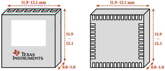
Figure 8.
The parameters of LMG3422R050 from TI’s datasheet.
The power density can be calculated as follows: the device is encapsulated in a low-inductance 12 mm × 12 mm VQFN (very thin Quad Flat No-lead package) package with a thickness of only 1 mm, making it well-suited to maximizing the heat-spreading area while minimizing parasitic effects. The total volume can be calculated as
Based on the device specifications, the maximum continuous RMS current is 32 A under a typical DC bus voltage of 400 V. Therefore, the achievable output power is
The resulting power density is then calculated by
According to the power density calculation, the LMG3422R050 is an ideal power switch with high power density under a flattened converter design methodology.
A counterexample is the MOSFET C3M0032120K from Wolfspeed. Although it is capable of handling high voltages of up to 1200 V and provides low on-resistance characteristics, the device is packaged in a standard TO-247-3 form factor, which significantly limits its power density compared to advanced integrated GaN solutions such as the LMG3422R050. The TO-247-3 package, with its large footprint and greater parasitic inductance, is less suitable for flattened PCB layouts and compact thermal designs. Furthermore, traditional SiC MOSFETs require external gate drivers and additional protection circuits, resulting in increased system complexity and larger overall volume. This highlights the advantages of using highly integrated GaN power stages for achieving superior power density and thermal performance in next-generation converter designs.
3.2. Power Inductor
The selection and design of appropriate inductors is essential to ensure that the converter meets the required performance in terms of output voltage quality, electromagnetic compatibility (EMC), and system stability []. In the proposed converter design, the output AC side inductors are carefully designed based on the targeted switching frequency, load characteristics, and thermal constraints.
In order to further enhance the compactness and thermal performance of the flattened power converter, planar inductors are employed in the filter and energy storage stages []. Unlike traditional wire-wound inductors, planar inductors utilize flat copper traces or multilayer laminations embedded within PCB structures or magnetic cores, resulting in a significantly lower profile and improved heat dissipation. Their inherently low DC resistance (DCR) and high-frequency performance make them particularly well-suited for the high switching speeds enabled by GaN-based devices. By integrating planar inductors into the flattened layout, the overall system thickness can be minimized without sacrificing magnetic performance, while simultaneously improving the thermal conduction paths through the large copper areas. This approach aligns with the flattened design philosophy by enabling higher power density, better manufacturability, and superior thermal management in high-efficiency power electronic systems. The following Figure 9 shows the different types of planar inductor winding and the prototype of the planar inductor.
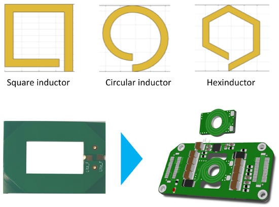
Figure 9.
Different types of planar inductor winding and the prototype of the planar inductor.
In the planar inductor design, the geometry of the winding significantly affects both electromagnetic and thermal performance. The most commonly adopted geometries include square, circular, and hexagonal shapes. Each offers unique advantages in terms of layout efficiency, field distribution, and manufacturability []. Square windings are widely used due to their ease of fabrication using standard PCB processes and their efficient area utilization on rectangular boards. Their layout naturally aligns with that of other power converter components, making them well-suited for compact integration. However, the sharp corners inherent to square geometries introduce localized current crowding and eddy current losses, which can degrade efficiency and lead to thermal hotspots if not properly mitigated with sufficient copper planes and thermal vias. Circular windings, on the other hand, exhibit the most uniform magnetic field distribution and lowest core loss due to the smooth and continuous current path. These structures are ideal for minimizing high-frequency losses and ensuring thermal uniformity. Nevertheless, circular layouts typically result in the underutilization of available PCB area, particularly in corner regions, and may complicate mechanical alignment with square-shaped magnetic cores or the surrounding circuitry. Hexagonal windings offer a geometric compromise between the square and circular forms. They provide improved magnetic symmetry compared to square windings while maintaining better area coverage than circular designs. Hexagonal structures can reduce parasitic effects and distribute heat more evenly, although they require more advanced fabrication techniques and may require custom-shaped cores [].
To address the potential increase in electromagnetic interference (EMI) resulting from the compact planar layout and high-frequency GaN switching, future versions of the converter design will incorporate planar EMI filters. Unlike traditional bulky filters, planar EMI filters can be integrated directly into the PCB stack-up or fabricated using laminated magnetic structures, enabling effective common-mode and differential-mode noise suppression without compromising the flattened form factor. These filters are particularly advantageous for surface-mounted power converters as they minimize parasitic effects, reduce loop area, and improve high-frequency attenuation. In [], a planar EMI filter was designed and tested to alleviate the EMI noise between the power switches and load 50%.
In addition to the electromagnetic analysis from the magnetic components perspective and the thermal analysis from the power management perspective, a mechanical analysis is also crucial for the power converter design. A thicker power board provides enhanced resistance to bending, vibration, and shock, making it ideal for demanding environments. Conversely, thinner boards offer flexibility but may be more susceptible to damage under physical stress. The optimal PCB thickness selection and number of layers are critical considerations during the design process, balancing the mechanical requirements of the application with other factors, such as electrical performance, thermal management, and manufacturing constraints. Typically, a 1.6 mm thickness for the PCB provides enough mechanical strength and a four-layer copper configuration is sufficient to provide both ground, EMI shielding, and up to 40 A current capacity to support 20 kW power delivery (with 2 oz copper).
Based on the above analysis, Table 1 presents a comparison between a planar inductor design and traditional design.

Table 1.
Comparison between planar design and traditional cube design.
3.3. Power Capacitor
The capacitor is another critical filtering component to mitigate the large voltage and current ripples on both the AC and DC sides. Typical types of capacitors that are commonly used for power electronic systems include ceramic capacitors, film capacitors, and electrolytic capacitors, as shown in Figure 10. Among the three types of capacitors used for power electronics applications, the ceramic capacitor is the smallest, with the lowest capacitance value. The electrolytic capacitor is the largest, with the highest capacitance value, and the film capacitor is in the middle, between the ceramic and electrolytic capacitors, in terms of volume and capacitance. The flattened power converter design requires the lowest height of the capacitors when being placed on the power board. The ceramic capacitor is the ideal option, with the lowest volume and a lower height than the other two types of capacitors. A three-dimensional comparison between a film capacitor and ceramic capacitor is shown in Figure 10. It can be seen that the height of the ceramic capacitor is four times lower than that of the film capacitor under a similar voltage and similar current ratings.
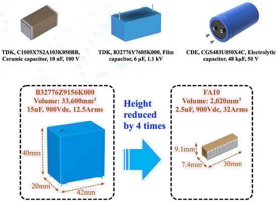
Figure 10.
Different types of capacitor and the flattened-design-oriented capacitor selection with a ceramic capacitor.
3.4. Digital Signal Processor
The digital control unit plays a crucial role in coordinating the operation of the flattened power converter by executing real-time control algorithms, protection strategies, and communication tasks. In this design, a dedicated digital controller is selected to achieve high-speed data processing, precise PWM generation, and reliable fault-handling. The controller features multiple high-resolution ADCs for the accurate sensing of voltages, currents, and temperatures, enabling closed-loop feedback control with minimal latency. To align with the flattened architecture, the control card is designed with a compact multilayer PCB layout, minimizing the vertical height while optimizing signal integrity and thermal dissipation. Key components, such as the micro-controller or DSP, gate drive signal isolators, and communication interfaces, are strategically placed to reduce loop inductance and electromagnetic interference (EMI). Additionally, the control card includes integrated protection functions, such as overcurrent detection, undervoltage lockout (UVLO), and thermal monitoring, which ensure safe operation at the GaN power stage. Through careful design and integration, the control card enables precise and efficient control of the power stage while maintaining the overall low-profile form factor of the flattened system. Under flattened designing methodology, the micro-controllers from the C2000 series of the Texas Instrument are ideal; they are also commonly used in industry, such as the TMS28379D and TMS28377D.
3.5. Other Promising Techniques
In addition to geometric optimization, substrate selection also plays a critical role in enhancing thermal performance in flattened converter designs. One widely adopted solution in state-of-the-art power converters is the use of Insulated Metal Substrates (IMS). IMS consist of a thin layer of dielectric bonded between a copper circuit layer and a thermally conductive metal base, typically aluminum. This structure offers significantly lower thermal resistance compared to standard FR4 or multilayer PCBs, enabling efficient heat conduction away from surface-mounted power devices []. For flattened power converters, where vertical height is constrained and passive cooling is emphasized, IMS enables more effective thermal spreading across the converter’s surface area, reducing local thermal gradients and minimizing the need for bulky heat sinks. Furthermore, IMS substrates are particularly compatible with wide-band gap devices such as GaN and SiC, which benefit from tight thermal control due to their high switching frequencies and power densities. By integrating IMS into the proposed layout, future iterations of the converter can further reduce junction temperatures and enhance long-term reliability without increasing volume [].
4. Experimental Demonstration
In high-power-density layouts, the thermal influence between adjacent components—known as mutual thermal coupling—can significantly impact local temperature increases. In our converter design, this was qualitatively addressed by maintaining adequate spacing between major heat sources (e.g., GaN switches and filter inductors), using thick copper planes to enhance lateral heat spreading, and avoiding thermal “bottlenecks” in high-current zones [].
For the reduction in thermal coupling among the power switches, the following methods can be implemented: (1) derive the optimal space among the power switches using ANSYS iteration; (2) configure multi-layer PCB with internal copper planes to spread heat more evenly; (3) leverage the enhanced cooling method to more effectively distribute the switching heat; (4) utilize optimal load and power sharing control among the parallel power switches for better switching power loss distribution.
The proposed flattened power electronic design methodology was validated through experimental testing. A prototype has been developed to demonstrate the effectiveness of the designed power converter structure, which was configured as a 20 kW three-phase DC/AC inverter. The converter operates at a switching frequency of 100 kHz. The active power and reactive power control follow the control diagram shown in Figure 11 in the d and q reference frames, respectively. Specifically, the active power and reactive power were first calculated based on the sampled AC voltage and current values. Then, the sampled active/reactive power values were compared with the corresponding references and imported into the power controllers. Following the power controllers are the AC output-side current controllers in d and q reference frames, which regulate the grid-side current values. Finally, the duty cycles were derived from the current controllers and transformed from the d and q reference frame back to the reference frame for the pulsed-width modulation (PWM) to generate the switching signals. The corresponding experimental results are presented in Figure 12, where the measured waveforms, from top to bottom, include the output AC current, output AC voltage, DC current, and DC voltage. The developed prototype achieves a power density of 15 kW/L, which is approximately twice that of conventional cubic block-shaped power converter designs, thereby validating the advantages of the proposed flattened architecture. A specification of the prototype is shown in Table 2.
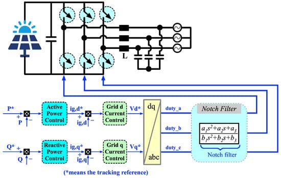
Figure 11.
Diagram of power control and notch filter-based power quality improvement.
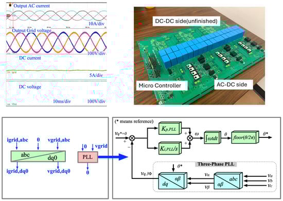
Figure 12.
Experimental waveforms of output AC current, output AC voltage, DC current, DC voltage, and the prototype.
Table 2.
Prototype Configurations.
For the power management and temperature distribution of the power converter board, the following equations are leveraged to connect between the delivered active/reactive power, , and the voltage and current in reference frame, , and :
The reactive and active power control diagram in Figure 11 demonstrate the process used to achieve the targeted power demand. The trace width of the PCB power routing determines the current conduction capability. Once the desired power level and grid-connected rated voltage are configured, the needed maximum load current is determined for the trace width design. The typical design process for the flattened power converter is shown in Figure 13. Firstly, the converter configuration is designed to determine the type and topology of power converter. Then, the component selection process is implemented to determine the high-power components of power switches, capacitors, and inductors, and low-power components of gate drivers, voltage/current sensors, power supplies, DSP, etc. Thirdly, the schematic is designed to specify the connections among the components, grounding and powering the configurations. Fourthly, the PCB is designed to finish the hardware layout, current, signal tracing, and isolation between the high-power and low-power areas. Lastly, the experimental test is demonstrated for validation.
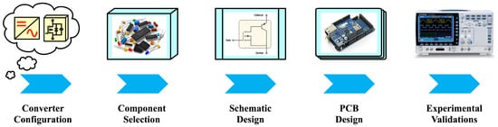
Figure 13.
Power converter design procedures.
The proposed flattened power converter design method is also compared with the state-of-the-art. Refs. [,,,,] designed the power converters to achieve high power-density. Specifically, ref. [] optimized the three-phase DC-AC inverter with SiC MOSFET and the soft switching strategy with a power-density of 6.6 kW/L and efficiency of 98.6% at 20 kW. Ref. [] designed the GaN-based three-phase power converter at 10 kW with a higher power density of 17.5 kW/L. Ref. [] also leveraged the GaN HEMTs to demonstrate a three-phase inverter prototype at 1.5 kW rated power and 97% efficiency. Ref. [] developed another on-board active rectifier and DC-DC converter to interface the receiver coil of a 50 kW EV inductive power transfer system with SiC MOSFET. The power density and efficiency were reported to be 9.5 kW/L and 98.6%, respectively. Furthermore, ref. [] designed a 10 kW EV charger that can be interfaced with the PV panel and the grid utility for charging. Since the extra solar integration function was included, the power density was relatively low, at 0.396 kW/L, with a peak efficiency of 96.4%. To summarize, the flattened power converter achieved 1.5–2 times higher power density and 2–3% higher efficiency than the state-of-the-art technologies.
In addition to the solar panel application that is to be connected to the grid, the designed flattened power converter can also be used to interface with the EV battery as the on-board or off-board EV charger. Since the on-board charger is integrated inside the vehicle, with limited space, the power density is of primary importance to deliver high power within the EV. The flattened power converter design can perform a compact battery charging and discharging as the onb-board charger. Additionally, the flattened power converter design method can be leveraged for more electric aircraft (MEA) applications to save space in the air for electrified transportation.
The adaptive thermal management strategies such as dynamic power limiting or real-time heat redistribution can further improve the energy conversion performance of the flattened power converter system. Specifically, the temperature sensors can be placed at the heat-concentrated areas of the power board to monitor the temperature variation. If more heat is generated or the temperature of the local area is increasing rapidly, the power controller in Figure 12 will respond by reducing the power demand to cool the hot area.
In addition to the adaptive thermal management, the fault tolerance capability is another factor that affects the reliability of the power converter. Due to the high-power application of the designed power converter (up to 20 kW), any fault on the switches, magnetics, sensors, gate drivers, or power supplies can result in the power failure of the whole system. Redundant power routing and switches can be configured so that the potential fault condition is tolerated. By monitoring the voltage and current abnormal conditions in the sampling information, the corresponding fault power branch can be diagnosed and replaced with redundant components. Through doing so, the fault tolerance capability and reliability can be enhanced.
5. Conclusions
This paper presents a novel flattened power converter design methodology aimed at improving both power density and thermal management performance in power electronic systems. By rethinking the structural configuration and changing it from a traditional cubic form to a flattened layout, the effective surface area for heat dissipation is significantly enlarged without increasing the system volume. Through careful component design and selection, including GaN-based power switches, planar magnetic components, ceramic capacitors, and compact control cards, the proposed design enhances system efficiency, thermal performance, and reliability. A 20 kW three-phase inverter prototype was developed and experimentally validated, achieving a power density of 15 kW/L—approximately twice that of conventional cubic block designs. The experimental results confirm that the flattened design not only meets the electrical performance requirements but also substantially reduces thermal stress and cooling system size. This work demonstrates the feasibility and advantages of adopting flattened architectures in next-generation, high-density, high-efficiency power conversion applications.
Author Contributions
Conceptualization, L.Z.; Methodology, L.Z.; Software, S.Z.; Validation, Z.D.; Formal analysis, Z.D. and S.Z.; Writing—review & editing, Z.D.; Supervision, L.Z. All authors have read and agreed to the published version of the manuscript.
Funding
This research received no external funding.
Data Availability Statement
The original contributions presented in the study are included in the article, further inquiries can be directed to the corresponding author.
Conflicts of Interest
The authors declare no conflict of interest.
References
- Kozlowski, M. Wound Rotor to Induction Motor and VFD Conversion Case Study. IEEE Trans. Ind. Appl. 2013, 49, 1221–1227. [Google Scholar] [CrossRef]
- Valenzuela, M.A.; Reyes, P. Simple and Reliable Model for the Thermal Protection of Variable-Speed Self-Ventilated Induction Motor Drives. IEEE Trans. Ind. Appl. 2010, 46, 770–778. [Google Scholar] [CrossRef]
- Du, S.; Wu, B.; Zargari, N. A Control Strategy for Star-Channel Modular Multilevel Converter in Variable-Speed Motor Drive Application. IEEE Trans. Ind. Electron. 2019, 66, 5094–5101. [Google Scholar] [CrossRef]
- Chalmers, B.; Musaba, L.; Gosden, D. Variable-frequency synchronous motor drives for electric vehicles. IEEE Trans. Ind. Appl. 1996, 32, 896–903. [Google Scholar] [CrossRef]
- Liu, Z.; Zhang, B.; Zhou, K.; Yang, Y.; Wang, J. Virtual Variable Sampling Repetitive Control of Single-Phase DC/AC PWM Converters. IEEE J. Emerg. Sel. Top. Power Electron. 2019, 7, 1837–1845. [Google Scholar] [CrossRef]
- Zanchetta, P.; Degano, M.; Liu, J.; Mattavelli, P. Iterative Learning Control with Variable Sampling Frequency for Current Control of Grid-Connected Converters in Aircraft Power Systems. IEEE Trans. Ind. Appl. 2013, 49, 1548–1555. [Google Scholar] [CrossRef]
- Liu, Z.; Zhou, K.; Yang, Y.; Wang, J.; Zhang, B. Frequency-Adaptive Virtual Variable Sampling-Based Selective Harmonic Repetitive Control of Power Inverters. IEEE Trans. Ind. Electron. 2021, 68, 11339–11347. [Google Scholar] [CrossRef]
- Li, Z.; Guo, Y.; Xia, J.; Li, H.; Zhang, X. Variable Sampling Frequency Model Predictive Torque Control for VSI-Fed IM Drives Without Current Sensors. IEEE J. Emerg. Sel. Top. Power Electron. 2021, 9, 1507–1517. [Google Scholar] [CrossRef]
- Chiriac, V.; Lee, T.Y.T. System-Level Thermal Performance Optimization for Electronic Module Incorporating Dual-Channel Power Stage For Digital Amplifier. In Proceedings of the Thermal and Thermomechanical Proceedings 10th Intersociety Conference on Phenomena in Electronics Systems, 2006, ITHERM 2006, San Diego, CA, USA, 30 May–2 June 2006; pp. 380–386. [Google Scholar] [CrossRef]
- Schmitt, W.; Duch, S.; Krebs, T. Comparison of Thermal Measurement Methods of Die Attach Materials Used in Power Electronic Modules. In Proceedings of the 2016 IEEE 66th Electronic Components and Technology Conference (ECTC), Las Vegas, NV, USA, 31 May–3 June 2016; pp. 1905–1911. [Google Scholar] [CrossRef]
- Weaver, W. Electro-thermal modeling, control and optimization in power distribution networks. In Proceedings of the 2010 12th IEEE Intersociety Conference on Thermal and Thermomechanical Phenomena in Electronic Systems, Las Vegas, NV, USA, 2–5 June 2010; pp. 1–7. [Google Scholar] [CrossRef]
- Ahmadi, B.; Bigham, S. PCM-impregnated heat sinks for transient thermal management of GaN electronic chips. In Proceedings of the 2024 23rd IEEE Intersociety Conference on Thermal and Thermomechanical Phenomena in Electronic Systems (ITherm), Aurora, CO, USA, 28–31 May 2024; pp. 1–6. [Google Scholar] [CrossRef]
- Liu, Z.; Zhang, B.; Zhou, K.; Wang, J. Virtual Variable Sampling Discrete Fourier Transform Based Selective Odd-Order Harmonic Repetitive Control of DC/AC Converters. IEEE Trans. Power Electron. 2018, 33, 6444–6452. [Google Scholar] [CrossRef]
- Kukrer, O.; Komurcugil, H. Variable sampling frequency PWM waveforms. IEEE Power Electron. Lett. 2003, 1, 14–16. [Google Scholar] [CrossRef]
- Herrán, M.A.; Fischer, J.R.; González, S.A.; Judewicz, M.G.; Carugati, I.; Carrica, D.O. Repetitive Control with Adaptive Sampling Frequency for Wind Power Generation Systems. IEEE J. Emerg. Sel. Top. Power Electron. 2014, 2, 58–69. [Google Scholar] [CrossRef]
- McGrath, B.; Holmes, D.; Galloway, J. Power converter line synchronization using a discrete Fourier transform (DFT) based on a variable sample rate. IEEE Trans. Power Electron. 2005, 20, 877–884. [Google Scholar] [CrossRef]
- Meng, Y.; Sun, J.; Duan, Z.; Jia, F.; Wang, X.; Wang, X. Variable Voltage Variable Frequency Modular Multilevel AC/AC Converter with High-Frequency Harmonics Filtering Capability. IEEE J. Emerg. Sel. Top. Power Electron. 2022, 10, 811–821. [Google Scholar] [CrossRef]
- Chen, T.; Yu, R.; Huang, A.Q. Variable-Switching-Frequency Single-Stage Bidirectional GaN AC;DC Converter for the Grid-Tied Battery Energy Storage System. IEEE Trans. Ind. Electron. 2022, 69, 10776–10786. [Google Scholar] [CrossRef]
- Panov, Y.; Jovanovic, M. Adaptive off-time control for variable-frequency, soft-switched flyback converter at light loads. IEEE Trans. Power Electron. 2002, 17, 596–603. [Google Scholar] [CrossRef]
- Chen, J.; Sha, D.; Zhang, J.; Liao, X. An SiC MOSFET Based Three-Phase ZVS Inverter Employing Variable Switching Frequency Space Vector PWM Control. IEEE Trans. Power Electron. 2019, 34, 6320–6331. [Google Scholar] [CrossRef]
- Lucía, O.; Burdío, J.M.; Millán, I.; Acero, J.; Barragán, L.A. Efficiency-Oriented Design of ZVS Half-Bridge Series Resonant Inverter with Variable Frequency Duty Cycle Control. IEEE Trans. Power Electron. 2010, 25, 1671–1674. [Google Scholar] [CrossRef]
- Chen, J.; Sha, D.; Zhang, J.; Liao, X. A Variable Switching Frequency Space Vector Modulation Technique for Zero-Voltage Switching in Two Parallel Interleaved Three-Phase Inverters. IEEE Trans. Power Electron. 2019, 34, 6388–6398. [Google Scholar] [CrossRef]
- Oñederra, O.; Kortabarria, I.; de Alegría, I.M.; Andreu, J.; Gárate, J.I. Three-Phase VSI Optimal Switching Loss Reduction Using Variable Switching Frequency. IEEE Trans. Power Electron. 2017, 32, 6570–6576. [Google Scholar] [CrossRef]
- Chen, J.; Sha, D.; Yan, Y.; Liu, B.; Liao, X. Cascaded High Voltage Conversion Ratio Bidirectional Nonisolated DC–DC Converter with Variable Switching Frequency. IEEE Trans. Power Electron. 2018, 33, 1399–1409. [Google Scholar] [CrossRef]
- Huang, Q.; Yu, R.; Ma, Q.; Huang, A.Q. Predictive ZVS Control with Improved ZVS Time Margin and Limited Variable Frequency Range for a 99% Efficient, 130-W/in3 MHz GaN Totem-Pole PFC Rectifier. IEEE Trans. Power Electron. 2019, 34, 7079–7091. [Google Scholar] [CrossRef]
- Cheng, C.H.; Chen, C.J.; Wang, S.S. An Adaptive Variable-Frequency Control with Constant Crossover Frequency Achieving Fast Transient Response for Wide-Operation-Range Flyback Converter. IEEE Trans. Power Electron. 2019, 34, 5537–5548. [Google Scholar] [CrossRef]
- Li, Y.; Ruan, X.; Zhang, L.; Dai, J.; Jin, Q. Variable Switching Frequency ON–OFF Control for Class E DC–DC Converter. IEEE Trans. Power Electron. 2019, 34, 8859–8870. [Google Scholar] [CrossRef]
- Dong, X.; Weisshaar, A. Design of Compact Integrated Lumped-Element Coupled-Resonator Filters. In Proceedings of the 2018 IEEE 27th Conference on Electrical Performance of Electronic Packaging and Systems (EPEPS), San Jose, CA, USA, 14–17 October 2018; pp. 289–291. [Google Scholar] [CrossRef]
- Dong, X.; Weisshaar, A. Compact Design of Passive Networks in RF and Millimeter-Wave Integrated Circuits (invited). In Proceedings of the 2021 IEEE BiCMOS and Compound Semiconductor Integrated Circuits and Technology Symposium (BCICTS), Monterey, CA, USA, 5–8 December 2021; pp. 1–4. [Google Scholar] [CrossRef]
- U.S. Department of Energy. EDTT Roadmap 2023: JOG Consensus Compliant; Technical Report; U.S. Department of Energy: Washington, DC, USA, 2024.
- Piramidowicz, R.; Stopiński, S. Exploring Photonic Integrated Circuits—Technologies, Applications and Challenges. In Proceedings of the 2024 31st International Conference on Mixed Design of Integrated Circuits and System (MIXDES), Gdansk, Poland, 27–28 June 2024; p. 16. [Google Scholar] [CrossRef]
- Brozek, T. Advanced Silicon Technologies: Design Consequences of Scaling Solutions for Devices. In Proceedings of the 2024 31st International Conference on Mixed Design of Integrated Circuits and System (MIXDES), Gdansk, Poland, 27–28 June 2024; pp. 11–14. [Google Scholar] [CrossRef]
- McDowell, A.J.; Hubing, T.H. A Compact Implementation of Parasitic Inductance Cancellation for Shunt Capacitor Filters on Multilayer PCBs. IEEE Trans. Electromagn. Compat. 2015, 57, 257–263. [Google Scholar] [CrossRef]
- Ge, J.; Zhao, Z.; Li, J. Backstepping control for active power filter with LCL filter. In Proceedings of the 2nd IET Renewable Power Generation Conference (RPG 2013), Beijing, China, 9–11 September 2013; pp. 1–4. [Google Scholar] [CrossRef]
- Tay, S.Y.; Adrian, V.; Chang, J.; Lee, J.; Gwee, B.H. A Versatile and Accurate Vector-Based Method for Modeling and Analyzing Planar Air-Core Inductors. In Proceedings of the 2022 IEEE International Symposium on Circuits and Systems (ISCAS), Austin, TX, USA, 27 May–1 June 2022; pp. 3063–3067. [Google Scholar] [CrossRef]
- Nejadpak, A.; Barzegaran, M.; Mohammed, O.A. Design of the high frequency electromagnetic behavior of planar inductor for resonant circuits in switching power converters. In Proceedings of the IET 8th International Conference on Computation in Electromagnetics (CEM 2011), Wroclaw, Poland, 11–14 April 2011; pp. 1–2. [Google Scholar] [CrossRef]
- Østergaard, C.; Kjeldsen, C.; Nymand, M.; Ramachandran, R. Simulation and measurement of AC resistance for a high power planar inductor design. In Proceedings of the 2019 IEEE 13th International Conference on Compatibility, Power Electronics and Power Engineering (CPE-POWERENG), Sonderborg, Denmark, 23–25 April 2019; pp. 1–5. [Google Scholar] [CrossRef]
- Zheng, S.; Wang, S.; Li, B.L. The application of multi-stage EMI filter design method in planar EMI filter. In Proceedings of the 2015 Asia-Pacific Symposium on Electromagnetic Compatibility (APEMC), Taipei, Taiwan, 26–29 May 2015; pp. 140–143. [Google Scholar] [CrossRef]
- Chowdhury, S.; Gurpinar, E.; Ozpineci, B. Characterization and Analysis of Insulated Metal Substrate-Based SiC Power Module for Traction Application. In Proceedings of the 2020 IEEE Energy Conversion Congress and Exposition (ECCE), Detroit, MI, USA, 11–15 October 2020; pp. 195–202. [Google Scholar] [CrossRef]
- Chen, Z.; Huang, A.Q. A SiC Power Module with Insulated Metal Substrate (IMS) and Improved Electromagnetic Interference (EMI). In Proceedings of the 2024 IEEE Energy Conversion Congress and Exposition (ECCE), Wroclaw, Poland, 11–14 April 2024; pp. 6709–6714. [Google Scholar] [CrossRef]
- Guo, W.; Ma, M.; Wang, H.; Chen, Q.; Wang, H.; Song, Q.; Chen, W. Decoupling Compact Thermal Model in Multichip IGBT Modules: A Methodology Based on Concepts of Positive and Negative Mutual Thermal Coupling. IEEE J. Emerg. Sel. Top. Power Electron. 2024, 12, 5476–5492. [Google Scholar] [CrossRef]
- He, N.; Chen, M.; Wu, J.; Zhu, N.; Xu, D. 20-kW Zero-Voltage-Switching SiC-mosfet Grid Inverter with 300 kHz Switching Frequency. IEEE Trans. Power Electron. 2019, 34, 5175–5190. [Google Scholar] [CrossRef]
- Li, H.; Zhang, X.; Zhang, Z.; Yao, C.; Qi, F.; Hu, B.; Wang, J.; Liu, L. Design of a 10 kW GaN-based high power density three-phase inverter. In Proceedings of the 2016 IEEE Energy Conversion Congress and Exposition (ECCE), Milwaukee, WI, USA, 18–22 September 2016; pp. 1–8. [Google Scholar] [CrossRef]
- Lautner, J.; Piepenbreier, B. High Efficiency Three-Phase-Inverter with 650 V GaN HEMTs. In Proceedings of the PCIM Europe 2016, International Exhibition and Conference for Power Electronics, Intelligent Motion, Renewable Energy and Energy Management, Nuremberg, Germany, 10–12 May 2016; pp. 1–8. [Google Scholar]
- Bosshard, R.; Kolar, J.W. All-SiC 9.5 kW/dm3 On-Board Power Electronics for 50 kW/85 kHz Automotive IPT System. IEEE J. Emerg. Sel. Top. Power Electron. 2017, 5, 419–431. [Google Scholar] [CrossRef]
- Chandra Mouli, G.R.; Schijffelen, J.; van den Heuvel, M.; Kardolus, M.; Bauer, P. A 10 kW Solar-Powered Bidirectional EV Charger Compatible with Chademo and COMBO. IEEE Trans. Power Electron. 2019, 34, 1082–1098. [Google Scholar] [CrossRef]
Disclaimer/Publisher’s Note: The statements, opinions and data contained in all publications are solely those of the individual author(s) and contributor(s) and not of MDPI and/or the editor(s). MDPI and/or the editor(s) disclaim responsibility for any injury to people or property resulting from any ideas, methods, instructions or products referred to in the content. |
© 2025 by the authors. Licensee MDPI, Basel, Switzerland. This article is an open access article distributed under the terms and conditions of the Creative Commons Attribution (CC BY) license (https://creativecommons.org/licenses/by/4.0/).