1. Introduction
The global transition toward decarbonized energy systems is being significantly accelerated by the widespread integration of distributed renewable energy resources (DERs), such as solar photovoltaic (PV) and wind power [
1]. However, the stochastic and intermittent nature of these energy sources introduces substantial challenges for grid stability, particularly in maintaining real-time supply–demand balance and frequency regulation [
2]. In this context, battery energy storage systems (BESSs) have emerged as critical enablers for delivering essential grid services, including dynamic regulation, peak shaving, and emergency backup through bidirectional energy conversion [
3]. By storing surplus renewable energy during periods of low demand and discharging it during peak load times, BESSs effectively mitigate the variability of renewable generation and facilitate its seamless integration into existing power grids [
4].
A typical BESS architecture comprises three core subsystems: the battery cell, the battery management system (BMS), and the power conversion system (PCS). These components work in synergy to ensure safe, efficient, and reliable operation. Recent advancements in battery technology have increasingly favored low-voltage, high-capacity configurations, primarily due to their cost-effectiveness and reduced complexity in BMS implementation [
5]. Commercial BESS applications commonly employ lithium iron phosphate (LFP) and nickel manganese cobalt (NMC)-based lithium-ion cells, which offer nominal voltages in the range of several volts [
6,
7]. These chemistries are widely adopted, owing to their superior energy density, extended cycle life, and enhanced thermal and electrochemical stability [
8]. Despite advantages such as lower material costs and reduced self-heating compared to high-voltage alternatives, these low-voltage battery technologies necessitate significant voltage step-up ratios within the PCS to interface with medium- or high-voltage grid infrastructure [
9]. This requirement has led to an increasing demand for high-efficiency, high-voltage-gain DC–DC converters—key components of the PCS—which are crucial for ensuring both the economic feasibility and operational efficiency of modern BESS architectures [
10].
To meet these technical demands, various DC–DC converter topologies have been developed and can be broadly categorized into non-isolated and isolated structures. Non-isolated converters—such as Buck, Boost, and Buck–Boost—are widely used for their simplicity and compactness; however, they face limitations in achieving high-voltage gain and sustaining efficiency under heavy-load conditions [
11,
12]. In contrast, isolated topologies—including Flyback, Push–Pull, Phase-Shifted Full-Bridge (PSFB), and LLC resonant converters—are preferred in high-power and safety-critical applications, due to their inherent galvanic isolation and improved reliability [
13,
14,
15,
16,
17]. Among them, LLC resonant converters achieve high efficiency over a wide load range but typically require complex magnetic designs and precise tuning of resonant parameters [
16,
17]. Alongside hardware innovations, numerous control strategies have been proposed to enhance converter performance in terms of efficiency, dynamic response, and robustness. Pulse Width Modulation (PWM) remains one of the most widely adopted techniques due to its simplicity and effectiveness, especially in high-frequency applications [
18,
19]. In full-bridge configurations, phase-shifted PWM enables zero-voltage switching (ZVS), thereby significantly reducing switching losses [
20,
21].
Among the various isolated bidirectional DC–DC converter topologies, the dual-active-bridge (DAB) converter has attracted considerable attention due to its symmetrical structure, galvanic isolation, and soft-switching capability, making it well suited for high-efficiency applications [
22,
23,
24]. A conventional DAB consists of two full-bridge circuits coupled via a high-frequency transformer (HFT), enabling precise power regulation through phase-shift modulation [
25,
26]. Recent research has focused on advanced control strategies such as dual-phase-shift (DPS) and triple-phase-shift (TPS), which reduce reactive power circulation and improve efficiency across different operating conditions [
27]. Enhanced schemes integrating offline optimization techniques have also been proposed, to minimize total losses by defining distinct power zones. Additionally, auxiliary methods like flux suppression and transient phase-shift control further enhance system robustness [
28]. As a core circuit in high-frequency power conversion systems, the DAB enables compact and efficient bidirectional energy transfer [
29]. In automotive applications, an optimized modulation strategy improved the average efficiency of a 2 kW DAB converter from 89.6% to 93.5%, demonstrating practical performance gains [
30]. These advancements reinforce the DAB’s role as a key topology for next-generation high-performance PCS.
Despite extensive research efforts dedicated to optimizing control strategies for the conventional DAB converter, its practical application in high-voltage-gain scenarios remains constrained by inherent limitations. Specifically, the voltage step-up ratio of the conventional DAB topology is limited to the turns ratio of the HFT, and the relatively large number of power semiconductor devices significantly increases the system cost, thereby diminishing its competitiveness in high-step-up applications. In contrast, a DAB converter based on symmetrical half-bridge voltage-doubler circuits presents a promising alternative for BESSs. This topology not only doubles the effective voltage gain, but also reduces the number of high-voltage-side switching devices by half, leading to substantial cost savings and enhanced economic viability. However, the reduction in bridge arms compromises the control degrees of freedom of the converter, rendering advanced TPS control—which achieves optimal performance in terms of ZVS and reactive power minimization in conventional DAB topologies—no longer applicable. Under DPS control, the output power range becomes more restricted, and it becomes increasingly challenging to simultaneously achieve ZVS across all switching devices and minimize circulating currents, thus limiting the converter’s ability to meet the stringent efficiency, reliability, and dynamic response requirements of modern BESS applications.
In light of these limitations, this paper proposes a novel control strategy specifically tailored for high-voltage-gain DAB converters based on symmetrical half-bridge voltage-doubler circuits.
Section 2 provides an overview of the considered DAB converter topology, including its operational principles and key circuit parameters.
Section 3 investigates the converter’s operational behavior under various modes, with particular emphasis on Modes B1 and C1, where simplified analytical methods are applied to evaluate the current stress and output power characteristics.
Section 4 details the optimized control strategies, addressing joint optimization of ZVS conditions and reactive power circulation under heavy-load scenarios, as well as comprehensive ZVS enhancement for light-load operations. A unified feedback control framework is introduced in
Section 5 to dynamically adjust control parameters based on real-time operating conditions, thereby ensuring system stability and optimal performance. Finally,
Section 6 validates the proposed control strategies through extensive simulation studies, demonstrating notable improvements in efficiency, reliability, and dynamic response—especially under extremely high voltage conversion ratios. The results can contribute to the advancement of high-performance power conversion technologies, facilitating the efficient integration of renewable energy and storage systems into modern power grids, and enhancing the overall economic viability and operational efficiency of BESS applications.
2. High-Voltage-Ratio Dual Active Bridge
2.1. Converter Topology
The high-voltage-ratio DAB topology under investigation, illustrated in
Figure 1, employs a symmetrical configuration with six power switches (
–
) to facilitate bidirectional energy conversion between a low-voltage battery terminal (
) and a medium-voltage DC bus (
). As shown in the schematic, the primary-side full-bridge circuit, constructed with
,
,
, and
, interfaces with the battery through an input capacitor (
), while the secondary-side hybrid network, constructed with
,
,
, and
, enables voltage multiplication via switched-capacitor operation. The drain–source voltages of
–
are denoted as
,
,
,
,
, and
, respectively. Galvanic isolation and voltage scaling are achieved through a high-frequency transformer with a turns ratio 1:
n, where the magnetizing inductance (
) governs core excitation dynamics and the secondary leakage inductance (
) dominates power transfer characteristics. Voltage stresses across switches are systematically mitigated: primary switches withstand
, while secondary switches experience halved stress (
/2), due to capacitive voltage division between
and
.
Phase-shift modulation between the primary and secondary bridges regulates the power flow by controlling the relative timing of (primary voltage) and (secondary voltage). The equivalent circuit, comprising , , and in series, reveals first-order linear dynamics that simplify the control design. To minimize magnetizing current distortion, is intentionally designed with a value significantly exceeding , ensuring the primary current predominantly mirrors the scaled secondary current (). This design choice effectively decouples the core excitation from power transfer dynamics, while preserving the soft-switching capability.
The topology demonstrates unique voltage adaptation capabilities through its hybrid design: the transformer’s turns ratio (
n) establishes baseline voltage scaling, while the switched-capacitor network (
,
,
, and
) provides additional voltage doubling. This cascaded approach allows the system to achieve total voltage gains of 2
n, while maintaining manageable voltage stresses on semiconductor devices. Such design considerations make this topology particularly suitable for battery energy storage systems requiring efficient, high-ratio bidirectional conversion between low-voltage battery stacks and medium-voltage DC grids. In
Figure 1, the reference directions for voltage and current indicate the power transmission from the battery side to the bus side.
2.2. Mode Classification
The control strategy is based on a DPS modulation scheme, which introduces two independent phase-shift angles: one between the half-bridges
/
and
/
, and another between
/
and
/
. This modulation generates a three-level waveform for
and a two-level waveform for
. As illustrated in
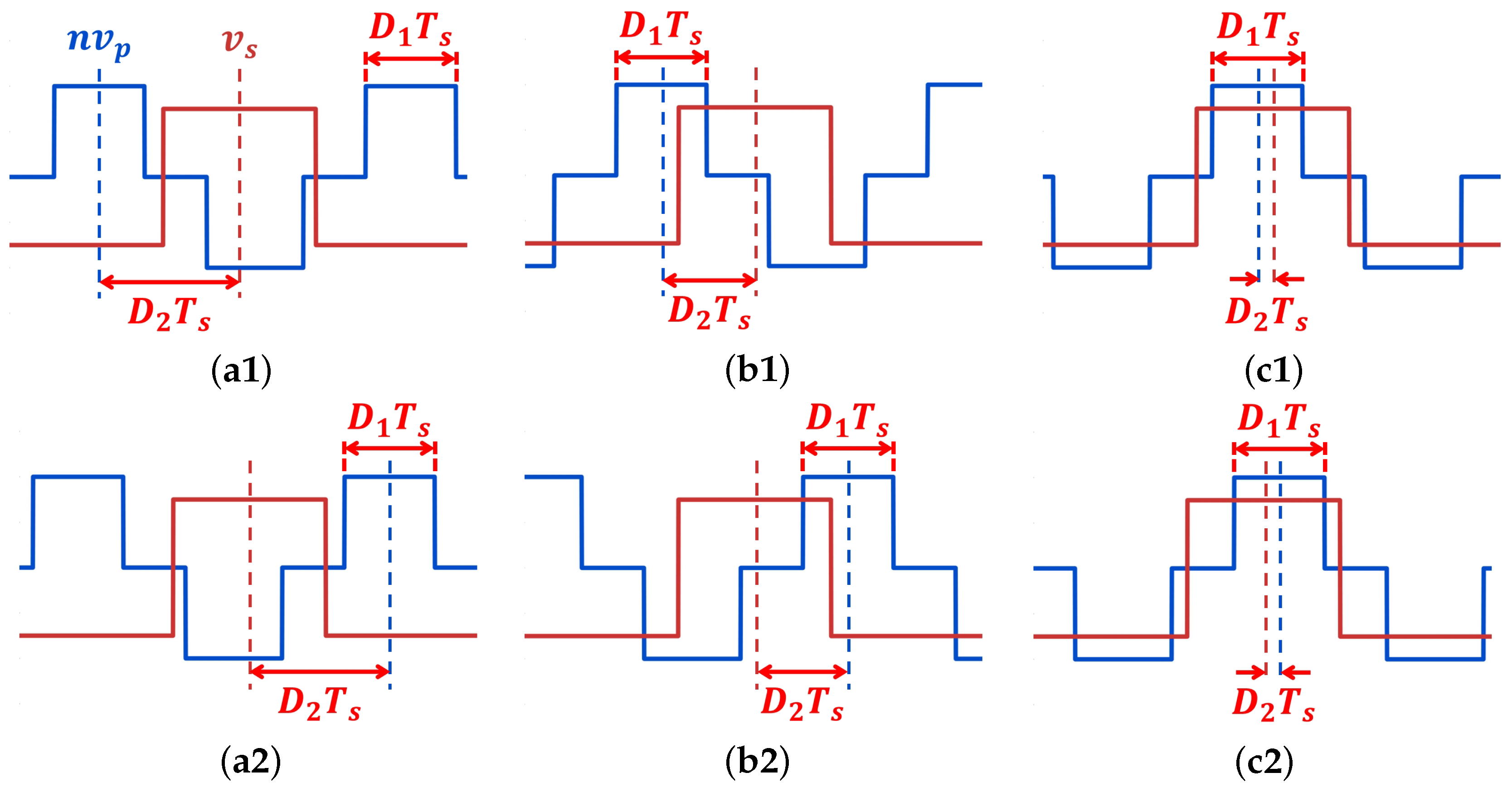
Figure 2, the DAB converter operates in six distinct modes, classified based on the relative alignment of the midpoint positions of the high-level voltage pulses between
and
.
Specifically, Modes A1 and A2 correspond to fully staggered high-level pulses, resulting in minimal overlap and hence limited power transfer capability. In contrast, Modes B1 and B2 exhibit partial overlap, enabling moderate power delivery with a controllable reactive current. Finally, Modes C1 and C2 feature full alignment of the voltage pulses, allowing maximum energy transfer under forward or reverse directions, respectively. For forward power transfer (i.e., from low-voltage side to high-voltage side), the midpoint of the high-level pulse consistently leads that of , creating a positive average voltage difference across the leakage inductance, which linearly drives the magnetizing current for energy transfer. These conditions define Modes A1, B1, and C1. Conversely, during reverse power transfer (e.g., for battery charging or grid feedback), the midpoint of lags behind that of , resulting in negative net voltage and current flow—corresponding to Modes A2, B2, and C2.
To facilitate quantitative analysis and closed-loop control, two key phase-shift parameters are defined: and . Here, represents the duration of the high-level interval of , while denotes the time by which the midpoint of the high-level pulse leads the midpoint of . If the midpoint of lags behind that of , takes a negative value. The switching period is denoted as .
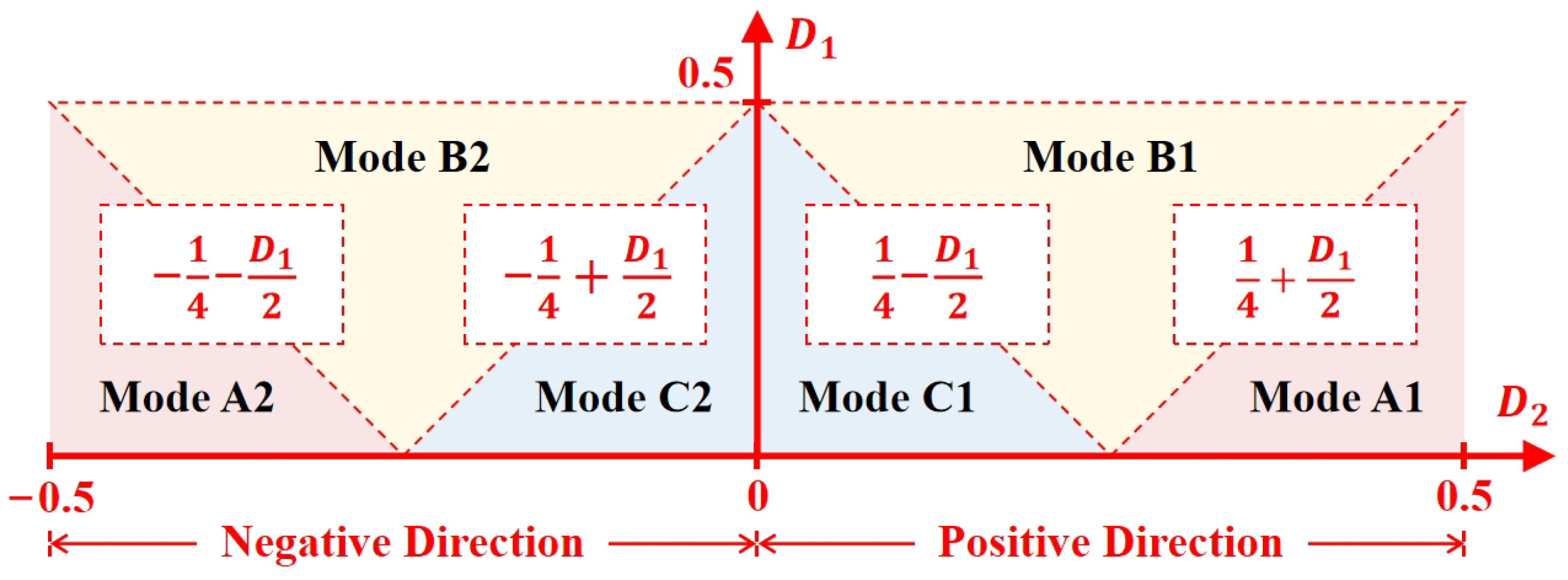
Furthermore,
Figure 3 illustrates the correlation of all operating modes with the phase-shift angles
and
, where
varies from 0 to 0.5, while
ranges from −0.5 to 0.5. For
, the converter operates in Mode A2, as depicted in
Figure 2(a2). In the range
, partial overlap between pulses activates Mode B2, corresponding to
Figure 2(b2). When
, full alignment of pulses characterizes Mode C2, as shown in
Figure 2(c2). For forward energy transfer (battery-to-bus),
corresponds to Mode C1, illustrated in
Figure 2(c1). The range
engages Mode B1, as depicted in
Figure 2(b1), while
activates Mode A1, as shown in
Figure 2(a1).
In practical implementations, the values of and must be carefully selected to ensure system stability and performance. Typically, ranges from 0.05 to 0.45, balancing between the required voltage gain and load conditions. Larger values increase the conduction interval of primary-side switches, enhancing the power transfer but also increasing switching losses. To avoid undesirable effects caused by dead-time insertion during switch transitions—such as waveform distortion and potential zero-crossing delays—the operating points of and should be chosen away from the mode boundaries. Maintaining a safety margin of approximately 0.05 in normalized phase-shift space from any mode boundary helps prevent timing mismatches and exceeding device tolerances, ensuring robust operation under varying load or input/output voltage conditions. This approach ensures predictable behavior, improved efficiency, and enhanced reliability in real-world applications.
3. Characteristic Operation Principle
Extensive research has been conducted on the current stress and output power performance of the dual-active-bridge (DAB) converter under various operating modes, e.g., [
22,
23]. These studies revealed that although Modes A1 and A2 can deliver the same output power range as Modes C1 and C2, they are associated with significantly higher RMS current stress. As a result, practical implementations typically avoid Modes A1 and A2, focusing instead on Modes B1, B2, C1, and C2 for efficient operation. Given the symmetry in waveform behavior between forward and reverse power transfer—e.g., between Modes B1 and B2 or C1 and C2—it suffices to analyze only the forward power transfer cases (Modes B1 and C1) without loss of generality.
This section presents a detailed analysis of the operational principles of Modes B1 and C1, followed by a comparative evaluation of their performance characteristics. For clarity,
Table 1 summarizes the units of measurement for all key variables used in this article.
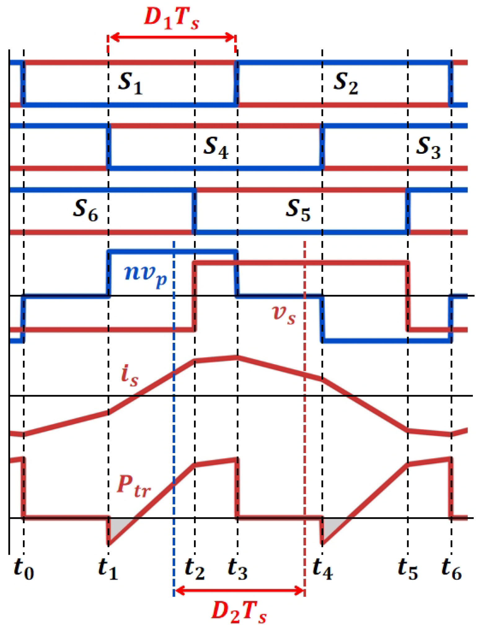
3.1. Operation Principle of Mode B1
Figure 4 illustrates the switching instants and voltage waveforms corresponding to
and
in Mode B1, assuming a negligible dead time. The phase-shift parameters are defined as follows:
The equivalent circuit for current dynamics consists of the primary-side reflected voltage , the leakage inductance , and the secondary-side voltage connected in series. The secondary-side current is governed by the voltage drop across . Based on the switching sequence, the following intervals define the operation of Mode B1:
From to : and are on, yielding , while conducts, resulting in . Consequently, increases linearly due to the positive voltage difference.
From to : turns on, setting , which further increases the voltage across , thereby accelerating the rise in .
From to : is activated, causing to transition to . Depending on the relative magnitudes of and , may continue to increase or begin to decrease.
Specifically, the time-domain expression for
is derived as follows:
Considering the symmetry of the
waveform within a switching cycle,
holds. Additionally, since
, and combining this with Equation (
1), the value of
at each switching instant can be determined as follows:
The waveform at the bottom of
Figure 4 represents the instantaneous transmission power of the transformer, calculated as
. The average output power delivered in Mode B1 is given by
Considering the feasible range of Mode B1 as described in
Figure 3, the output power
reaches its maximum value
when
and
. Mode B1 is particularly suitable for heavy-load conditions due to its high power delivery capability.
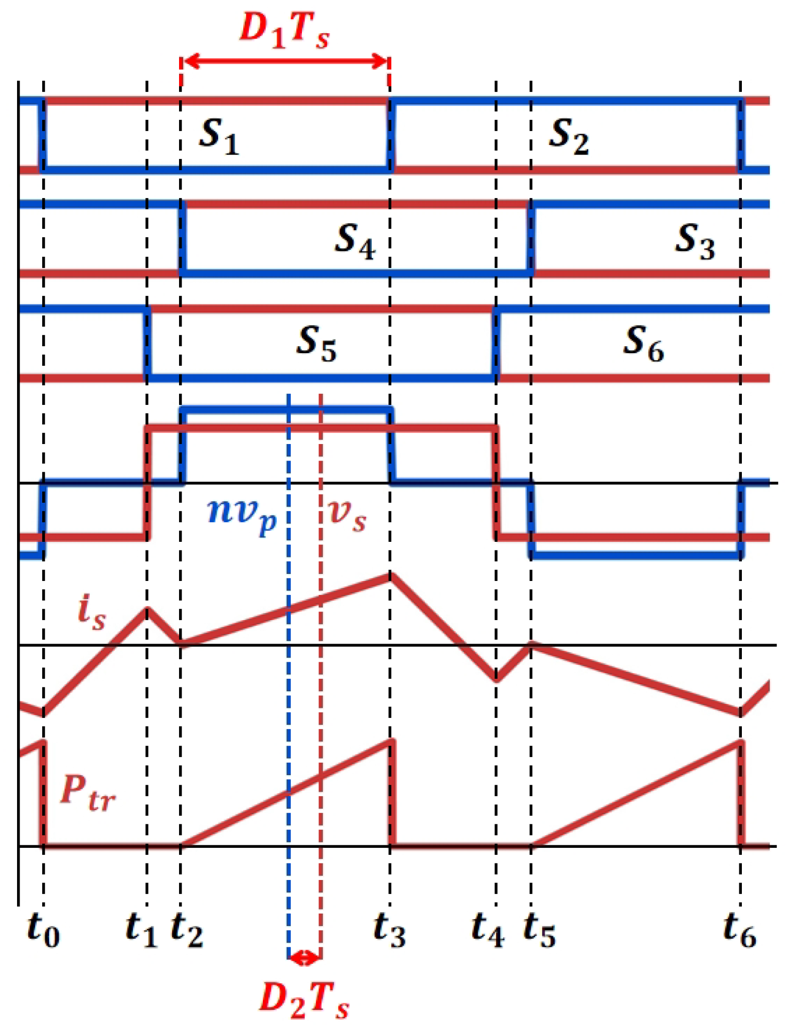
3.2. Operation Principle Mode C1
Figure 5 depicts the switching instants and voltage waveforms in Mode C1. The phase-shift parameters are defined as follows:
Similarly to Mode B1, the current dynamics are governed by the voltage across , and the operation is divided into three intervals:
From to : , , and are on, leading to and , which causes to increase.
From to : , , and are on, resulting in , hence decreases due to the negative voltage across .
From to : , , and conduct, and the slope of depends on the polarity of .
The time-domain equation for
in Mode C1 is
Using the waveform symmetry and Equation (
5), the current values at critical time points are
The average output power in Mode C1 is expressed as
When operating within the feasible region shown in
Figure 3, the output power
achieves its maximum value
when
and
. Compared to Mode B1, the peak power in Mode C1 is halved. However, this mode offers a lower current stress and is more suitable for light-load operation.
3.3. Comparative Analysis of Different Modes
To provide a comprehensive understanding of the operational differences between Modes B1 and C1,
Table 2 summarizes the key performance metrics. As observed from the table, Mode B1 exhibits superior output power capability but incurs higher current stress, making it ideal for high-power applications. In contrast, Mode C1 achieves lower conduction losses and improved ZVS performance, rendering it more suitable for low-to-medium power scenarios.
In summary, the choice between Modes B1 and C1 should be based on the specific application requirements, including load level, efficiency targets, and control complexity constraints. Subsequent sections will explore adaptive control strategies that dynamically switch between these modes to optimize system performance across varying operating conditions.
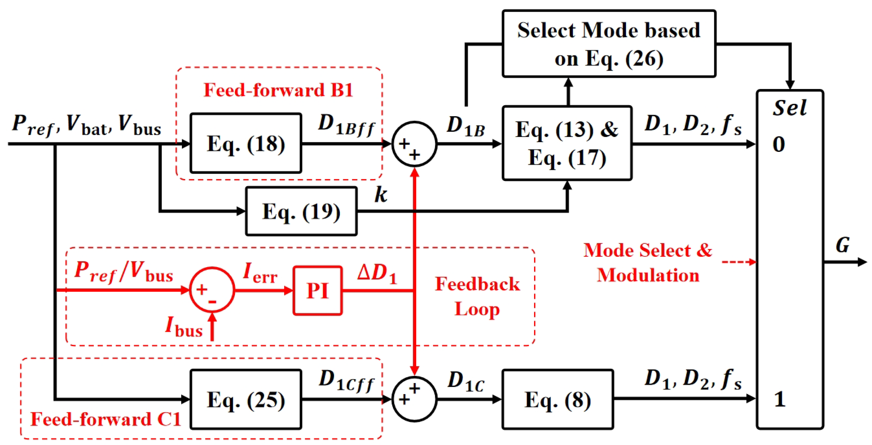
5. Control Methodology
To implement the proposed control strategies in real-time systems, a unified feedback control framework was developed to ensure system stability and optimize performance across all operating conditions. As illustrated in
Figure 6, the control architecture combines feed-forward and feedback mechanisms, to achieve stable and efficient operation under varying load conditions. Feed-forward control computes the initial phase shift angle based on the expected power flow and system parameters. For instance, Mode B1 utilizes Equation (
18) to calculate the feed-forward component
, while Mode C1 employs Equation (
25) to determine
. This predictive approach ensures rapid response to set-point changes and enhances the overall system responsiveness.
Feedback control further improves regulation accuracy by comparing the reference current with the measured bus current , generating an error signal . A PI controller processes this error to adjust the phase shift angle incrementally via , enabling fine-tuned response to dynamic load variations. This closed-loop mechanism ensures robustness and adaptability in practical applications.
The proportional coefficient
k is calculated using Equation (
19), which dynamically adjusts the switching frequency according to Equation (
17). To ensure smooth transitions between operating modes and avoid distortion caused by dead-time effects, a mode selection logic is implemented based on the following condition:
where
denotes the normalized dead-time duty cycle. If this inequality holds, Mode B1 is prioritized; otherwise, Mode C1 is selected. This logic guarantees continuous ZVS operation and avoids discontinuities during mode transitions.
This integrated control architecture eliminates abrupt transitions between different control loops, significantly enhancing system stability during rapid load changes. The modular design also allows for easy adaptation to various BESS configurations and environmental conditions, ensuring reliable and robust performance across diverse application scenarios.
6. Validation Through Simulation Results
To validate the effectiveness of the proposed control strategies, an extensive simulation study was conducted under a wide range of operating conditions. The simulation setup was based on a laboratory-scale DAB converter prototype, with detailed system parameters summarized in
Table 3. This configuration reflects typical design specifications applicable to portable BESS, making it suitable for integration into rooftop or balcony PV installations. The DAB converter was designed to interface a low-voltage battery stack, with an input voltage range of 20 V to 25 V, to a high-voltage DC bus regulated at 400 V. This wide voltage conversion ratio highlights the capability of the converter for handling demanding step-up requirements, while maintaining bidirectional power flow capability.
The switching frequency was dynamically adjusted according to the operational mode to optimize system performance. Specifically, a fixed switching frequency of 50 kHz was employed during Mode C1 operation. In contrast, under heavy-load conditions corresponding to Modes B1 and B2, the base switching frequency was set to 600 kHz. Based on Equation (
17), with a modulation factor
, the effective switching frequency varied between 300 kHz and 400 kHz. This adaptive frequency modulation strategy ensured efficient power transfer across the different operating modes, while preserving zero-voltage switching (ZVS) and minimizing circulating reactive power. These features collectively demonstrated the robustness and flexibility of the implemented control methodology.
Figure 7 presents the key operational waveforms under various voltage gain scenarios, including the primary-side voltage reflected to the secondary side of the transformer (
), the secondary-side voltage (
), the secondary-side current (
), and the transferred power (
). Specifically,
Figure 7(a1–a3) correspond to
with
, respectively, while
Figure 7(b1–b3) illustrate the corresponding waveforms for
under identical reference power levels. The DAB converter operated in Mode C1 for
and
, transitioning to Mode B1 when
reached
. At lower power levels, the system exhibited stable operation, with minimal voltage and current ripple. As the reference power was increased, a slight increase in ripple amplitude was observed; however, the overall regulation remained satisfactory, demonstrating the system’s capability to maintain performance under elevated load conditions. Under light-load conditions (Mode C1), the reactive circulating power was relatively high, to ensure complete ZVS across all switches. However, through the joint optimization of ZVS and reactive power minimization in Mode B1, the magnitude of the circulating power was significantly reduced, contributing to improved system efficiency, without compromising switching loss mitigation. Comparisons between waveforms corresponding to identical output powers but different input voltages revealed that a higher voltage conversion ratio necessitated a larger phase-shift duty cycle (
) to maintain the desired power transfer, highlighting the importance of optimizing
to accommodate varying voltage conversion ratios effectively.
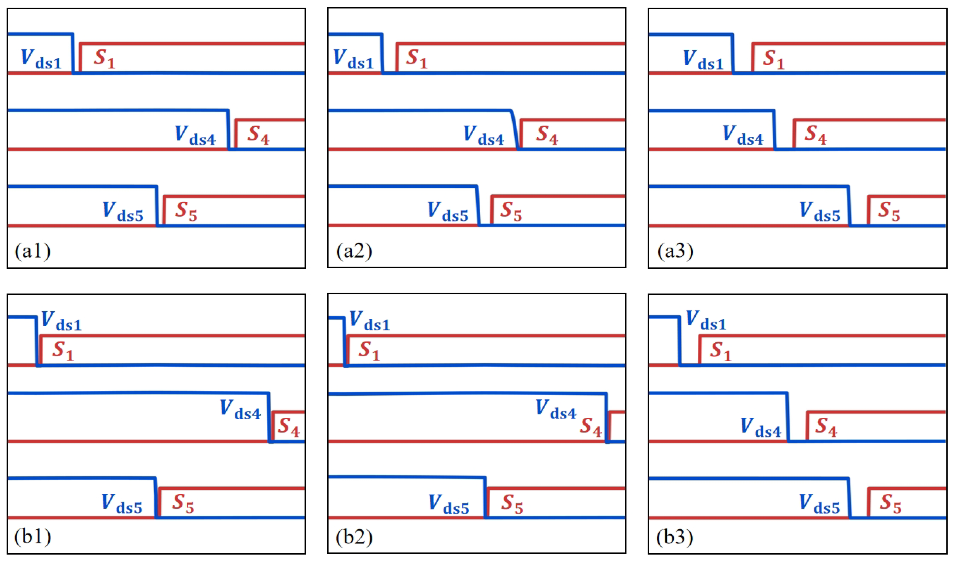
Figure 8 illustrates the ZVS performance under various operating conditions, showing the gate drive signals and drain-to-source voltages (
) for representative switches
,
, and
. Across all tested scenarios, ZVS was consistently achieved, as evidenced by the voltage across each switch reaching zero before turn-on, ensuring minimal switching losses and confirming the robustness of the proposed control methodology. The performance remained stable regardless of variations in battery voltage or reference power. Whether operating at low power levels (e.g., 100 W) or at full load (up to 500 W), and with battery voltages ranging from 20 V to 25 V, the system maintained reliable ZVS operation. A dead time of 100 ns was implemented between the turn-off and turn-on of two complementary switches within the same half-bridge to prevent shoot-through. In light-load conditions (Mode C1), the switching frequency was relatively low, making the dead-time duration appear proportionally narrow, due to the extended switching period. For instance, in
Figure 8(a2), the gradual decrease in
reflects the limited rate at which the parasitic capacitance of
was discharged by the small magnetizing current during the turn-on transition, underscoring the critical role of the transformer current in achieving reliable ZVS under low-power conditions. In contrast, under heavy-load conditions (Mode B1), the higher switching frequency makes the dead time appear wider relative to the shorter switching period. Nevertheless, the waveforms clearly indicate that each switch continued to operate under ZVS, thereby ensuring efficient energy conversion by minimizing switching losses.
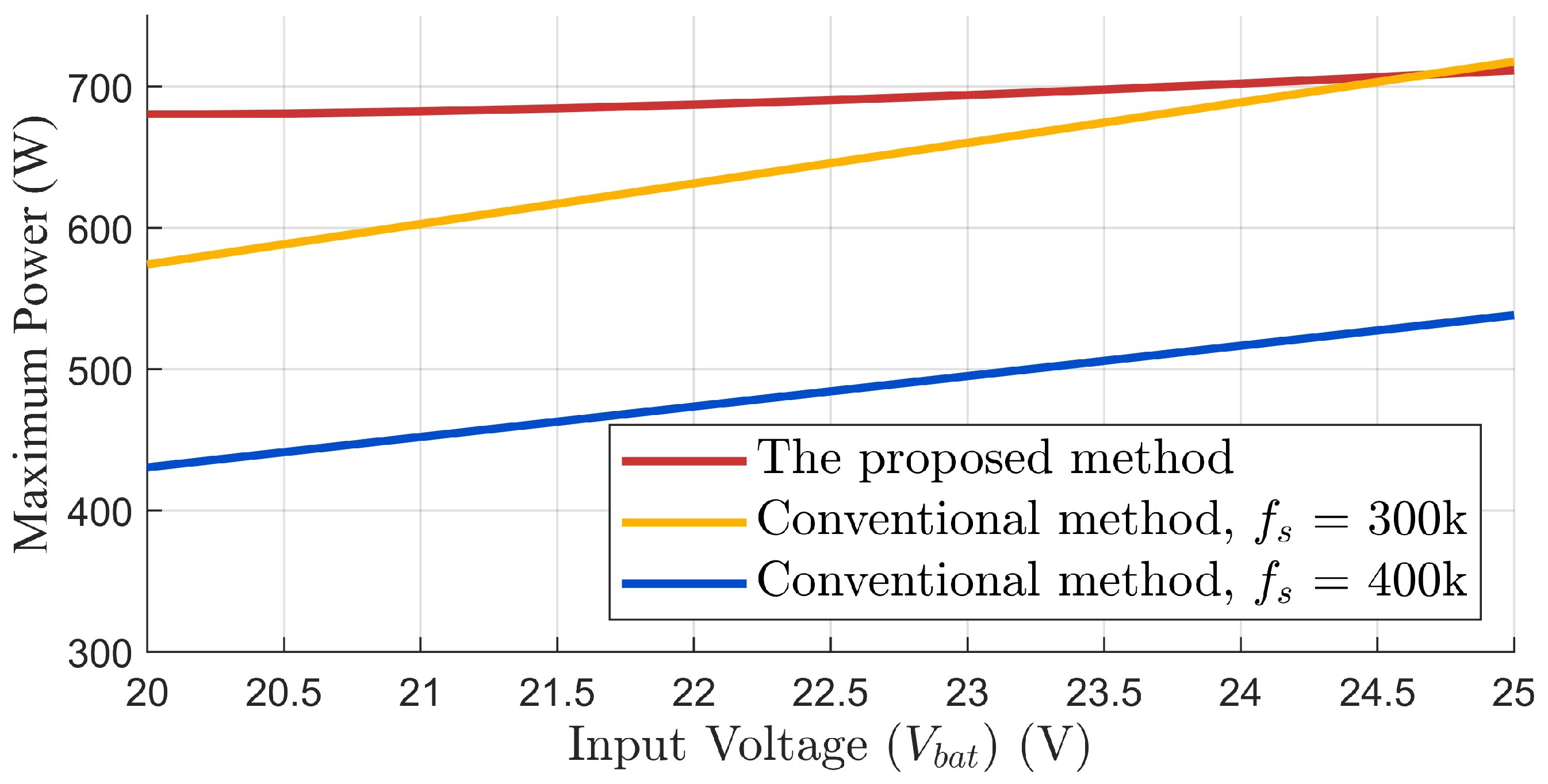
In addition to the operational waveform and ZVS validation, a comparative analysis was performed against conventional constant-frequency phase-shift control methods reported in the literature (e.g., [
22,
23]). Three distinct control approaches were evaluated under identical transformer parameters and input voltage conditions (20 V to 25 V): the proposed variable-frequency control scheme, a conventional fixed-frequency control at 300 kHz, and another at 400 kHz.
Figure 9 compares the maximum output power achievable across the input voltage range for all three strategies. The proposed method demonstrated superior overload capability throughout the entire voltage range, delivering a more than 35% overload margin. Specifically, at
, the converter achieved a peak output power of 680 W, while at
, the maximum output reached 711 W. In contrast, the conventional 300 kHz control exhibited a significantly reduced overload capacity, with less than 20% overloading margin at lower input voltages, and as low as 14.8% in some cases. Furthermore, the 400 kHz control failed to achieve the nominal 500 W output at
, delivering only 431 W, due to increased switching losses and limited modulation flexibility. By introducing frequency modulation as an additional degree of freedom, the proposed strategy enables an enhanced output power range and improved dynamic adaptability.
Beyond the output power capability, the ZVS performance and circulating reactive power were also compared. At under full load (), both the proposed method and the conventional 300 kHz control ensured complete ZVS across all switches. However, the proposed strategy reduced the circulating reactive power from 5.8 W to approximately 4.5 W, representing a 22.4% reduction. At , the conventional 300 kHz control failed to satisfy the ZVS constraints, as indicated by the unsolvable set of inequality conditions derived from the soft-switching boundary equations. On the other hand, the proposed method maintained robust ZVS performance, without compromising efficiency or stability.
Moreover, the proposed control methodology significantly reduces conduction losses by minimizing RMS current stress on semiconductor devices, particularly in comparison to traditional dual-phase-shift (DPS) methods. This is achieved without sacrificing soft-switching characteristics, thereby extending the device lifespan and reducing thermal stress. The integrated feedback mechanism further enhances system responsiveness to load variations, enabling fast transient recovery, without the need for complex mode-switching logic.
These combined advantages—enhanced output power range, improved efficiency, reduced conduction losses, and dynamic adaptability—render the proposed control methodology particularly well suited for battery energy storage systems (BESS), where wide-range power delivery, high efficiency, and reliable ZVS represent key design criteria. The integration of analytical derivation with real-time feedback control enables accurate tracking of power references and ensures robust system performance under both steady-state and transient operating conditions. The effectiveness of the proposed approach, especially in maintaining ZVS and minimizing circulating reactive power across a wide range of load variations, was substantiated through the comprehensive simulation studies presented above.
7. Conclusions
This paper presents an optimized control strategy for high-voltage-ratio DAB converters, specifically tailored for BESS. The proposed methodology integrates a precise circuit parameter design—including transformer turns ratio and leakage inductance—with advanced modulation techniques, which jointly optimize the switching frequency, as well as primary- and secondary-side phase shift ratios and . This comprehensive control framework enables full-range ZVS, significantly reduces the circulating reactive power, and minimizes current stress across semiconductor devices, thereby enhancing overall conversion efficiency.
Simulation results demonstrated the effectiveness of the proposed control scheme under a wide range of operating conditions. Under light-load operation (Mode C1), the system maintained ZVS across all switches with a fixed switching frequency of 50 kHz, achieving stable output regulation with minimal ripple. In contrast, during heavy-load conditions (Mode B1), the converter dynamically adjusted its switching frequency between 300 kHz and 400 kHz based on the modulation factor , ensuring efficient power transfer, while reducing the reactive circulating power by up to 22.4% compared to conventional fixed-frequency control strategies. At , the converter delivered a peak output of 680 W, exceeding the nominal 500 W requirement by more than 35%, showcasing its superior overload capability. These quantitative improvements underscored the system’s enhanced performance in terms of both steady-state efficiency and dynamic response.
The practical significance of this research lies in its potential to support next-generation portable BESSs integrated with rooftop or balcony PV installations. By enabling high-efficiency bidirectional power flow across extreme voltage conversion ratios (e.g., from 20 V to 400 V), the proposed control strategy facilitates compact, cost-effective, and thermally robust DAB converter designs. These characteristics are particularly valuable in distributed energy systems, where space constraints, thermal management, and long-term reliability are critical design considerations.
Future work will focus on refining analytical models for circuit parameter optimization and developing a hardware prototype to validate the simulation findings under real-world operating conditions. Experimental studies will quantify the impact of ZVS performance, circulating power, and conduction losses on overall system efficiency. Furthermore, the implementation of intelligent mode-switching logic will be explored to enhance the converter’s adaptability and ensure seamless transitions between operational modes. These efforts aim to bridge the gap between theoretical design and commercial deployment, advancing the application of high-efficiency DAB converters in sustainable energy systems.


