Abstract
Considering the cost, efficiency, power density, and other issues of the power electronic system, many papers have mixed the wide-bandgap (WBG) power devices, mainly SiC MOSFET and GaN FET/HEMT, with Si IGBT/MOSFET in the three-level active neutral-point clamped (T-ANPC) topology, forming the hybrid T-ANPC (HT-ANPC) topology. This paper reviews these latest HT-ANPC topologies from the perspective of the material types of switching devices and compares the advantages and disadvantages of various topologies. The potential challenges of HT-ANPC inverters in several mainstream applications are reviewed, and their improvements are compared and discussed in detail. Next, a brief topology selection and design process are provided based on analyzing various typical topologies. In addition, some future research trends on this topic are discussed. The paper will help researchers to select appropriate HT-ANPC topologies in different applications and have a better understanding of the critical issues to be considered during system design.
1. Introduction
In the field of power electronics, the inverter mainly plays a role in power conversion. In recent years, with the continuous development of power electronics technology, it has attracted the attention of many researchers as an indispensable unit. Based on the connection between the power supply and the load side, the inverter topologies in high-power applications can be categorized into two types: direct and indirect structures. In direct structures dominated by the cycloconverter and matrix converter, the power supply is directly connected to the load through power semiconductor devices. These topologies are unlikely to be used in high-voltage applications due to their limited dynamic performance, while the indirect structure uses energy storage elements between the power supply and the load. This type of structure can be further divided into current source type and voltage source type. The current source inverter (CSI) has disadvantages such as low power factor and waveform distortions [1,2]. Therefore, the voltage source inverter (VSI) is currently the most widely used.
Among VSIs, the advantages of multilevel inverters (MLIs) over two-level inverters are better output waveform quality, higher switching frequency, and more suitable for high-voltage and high-power applications. Therefore, MLIs are gradually replacing two-level inverters in various industrial applications, such as photovoltaic applications [3,4], electric propulsion systems [5,6], energy storage systems [7], and grid-connected systems [8,9]. Three-level topologies are one of the most popular structure categories used in MLIs. Among them, the T-Type neutral-point clamped (T-TNPC) topology and the diode neutral-point clamped (T-NPC) topology are the two most desirable structures. T-TNPC inverters are more favorable in applications with lower switching frequency requirements, while T-NPC inverters are more suitable for application scenarios with higher switching frequency requirements [10]. However, the device loss imbalance is particularly severe in the latter. This can limit the power rating and switching frequency of the system. Therefore, T. Bruckner et al. proposed the three-level active neutral-point clamped (T-ANPC) inverter [11]. This structure utilizes two active devices to replace the two diodes in the T-ANPC topology and mitigates the device junction temperature imbalance problem. The advantages and disadvantages of these topologies mentioned above have been analyzed in detail by R. Teichmann et al. [12,13].
In current industrial applications, especially in scenarios with high-power-density requirements, the advantages of the T-ANPC inverter composed of all-Si IGBTs are insignificant. As the research on WBG power devices gradually matures [14,15,16], they are widely used in the T-ANPC topology [17,18,19]. Such devices mainly include SiC MOSFET and GaN FET/HEMT, but they are expensive. Therefore, T.B. Soeiro et al. earlier proposed that the HT-ANPC inverter be composed of heterogeneous devices [20]. According to the different characteristics of devices, they selectively combine them in topologies. While significantly reducing system losses, it improves the efficiency of the inverter and considers the cost of the system. Hence, HT-ANPC inverters have more application prospects in current industrial applications.
For HT-ANPC inverters, some papers have undertaken comparative analyses on several types of topologies. No paper has conducted a comprehensive study on HT-ANPC inverters. Therefore, this paper provides a review from a rather thorough perspective centered around HT-ANPC inverters. A comprehensive summary of the combination of various types of switching devices in this current class of topologies is provided. The main challenges in several mainstream applications are discussed, as well as how to overcome them in detail. For example, for the HT-ANPC inverter to operate normally, selecting a suitable modulation strategy is essential. It can affect the switching loss, efficiency, and harmonic components of the output voltage of the system. In addition, in order to meet the high-efficiency goal of the power converter, the harmonic components at the output side should be reduced as much as possible to improve the output power quality. The combination of different types of switching devices will increase the complexity of the system and reduce the reliability of the stable operation of the system. These potential challenges will significantly affect the performance of the system and should be considered critical in the system design.
The main focus of this paper is shown in Figure 1. In order to have a clearer understanding of the advantages of HT-ANPC topologies, this paper first reviews the deduction from T-ANPC to HT-ANPC topologies in Section 2. Then, the operation modes, advantages, and disadvantages of HT-ANPC topologies are briefly analyzed, and their evolution is comprehensively summarized. At the end of Section 2, the modulation strategies are briefly discussed. Then, a detailed analysis of the potential challenges of HT-ANPC inverters in applications and their existing improvements is conducted in Section 3. In Section 4, a comprehensive comparative analysis of typical HT-ANPC topologies is provided, and a concise process performing topology selection and design is provided. Finally, future research trends of this topic are discussed, and the paper is concluded in Section 5 and Section 6.
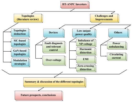
Figure 1.
Main focus in this paper.
2. Analysis of HT-ANPC Topologies
2.1. Topology Deduction
A comprehensive evaluation of the material properties of switching devices has been conducted in the paper [15]. SiC and GaN devices can operate at higher voltages and switching speeds than Si devices. SiC process technology is the most mature of the current WBG semiconductor materials, and it is more attractive for high-power electronic devices. Although GaN theoretically offers better high-frequency and high-voltage performance, the lack of high-quality bulk substrates required for vertical devices and lower thermal conductivity make SiC more suitable for high-voltage devices. It is worth noting that the inherent properties of GaN power devices also make them increasingly popular in industrial applications. In addition, in applications involving the WBG power devices, the typical high-cost issue is particularly critical, as shown in Table 1, which is more significant in Figure 2. For quantitative analysis, discrete devices in the 650 V/60 A rating have been sampled in Figure 2 to present a general trend in price. It can be seen that WBG devices are much more expensive than Si devices for the same power rating, especially at higher current ratings. Therefore, in recent years, HT-ANPC topologies formed by combining different material type devices have received increasing attention [20,21,22]. The proposed HT-ANPC topologies ameliorate the problem of the high cost of WBG devices, as shown in Table 1 for several modules from Infineon Technologies AG, Neubiberg, Germany.

Table 1.
Price comparison of different material type devices from INFINEON.
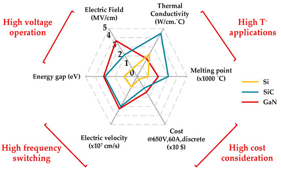
Figure 2.
Material properties for power devices.
In order to review the proposal of HT-ANPC topologies more clearly, this paper shows the deduction of T-ANPC topologies from homogeneous devices to heterogeneous devices, as shown in Figure 3. Taking into account the poor thermal performance and high loss of all-Si-type topologies, the high cost of all-SiC/GaN-type topologies, and the low voltage level of all-GaN-type topologies, HT-ANPC topologies were proposed [23].
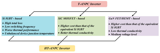
Figure 3.
Deduction from the T-ANPC inverter to the HT-ANPC inverter.
As shown in Figure 4, C. Li et al. proposed a generalized construction method for the hybrid multilevel ANPC topology [24,25]. They decoupled the structure into a low-frequency unit and a high-frequency unit, which mainly includes three parts: Voltage Generation Cell (VGC), LF Selection Network Cell (SNC), and HF Commutation Switch Cell (CSC). Where n represents the output voltage level, i represents that CSC rectifies between i terminals, that is, CSC always switches between i levels. The HT-ANPC topology derived by this construction method is also shown in Figure 4. In this paper, the six active devices are divided into three cells, and we comprehensively summarize the combination of switching devices in various HT-ANPC topologies in recent years in Section 2.
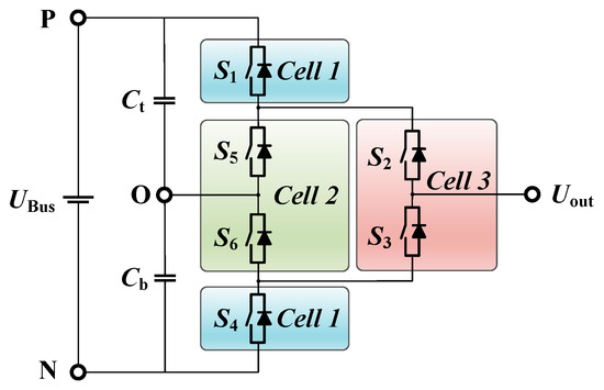
Figure 4.
Single-phase hybrid three-level ANPC converter.
2.2. SiC-Based Topologies
The SiC power devices included in HT-ANPC topologies are mainly SiC MOSFET and SiC Schottky Diode, among which SiC Schottky Diode is often connected in parallel with active devices to further reduce reverse recovery losses. In this paper, the HT-ANPC topologies involving SiC devices are classified into two categories, including regular topologies and some special topologies. The classification of regular topologies is mainly based on the number and position of SiC active devices included. It includes the A-type structure using two SiC MOSFETs, the B-type structure using four SiC MOSFETs, and the E-type structure using hybrid switches (HyS). Figure 5 shows the evolution of HT-ANPC topologies involving SiC power devices.
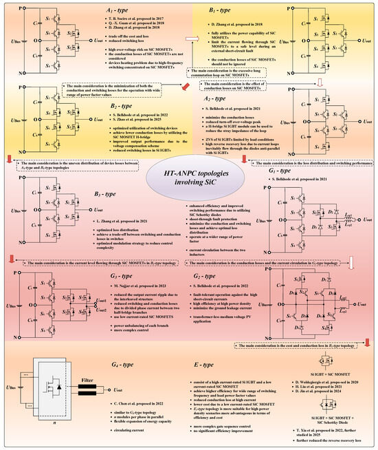
Figure 5.
Evolution of SiC-based HT-ANPC topologies.
Next, we will analyze each HT-ANPC topology from the perspective of topological structure, basic operating modes, and advantages and disadvantages, as shown in Table 2.
Table 2.
Combinations of devices in HT-ANPC topology.
2.2.1. Regular Topologies
A1-type
The A1-type topology, as the first HT-ANPC topology involving SiC devices, was proposed earlier by different research teams [20,21,22]. The proposal of this topology mainly considers the problem of the high-frequency-device heating of the T-ANPC topology composed of all-Si IGBTs and the high cost of the T-ANPC topology composed of all-SiC MOSFETs. Cell 3 in the topology uses SiC MOSFETs to further reduce switching losses and significantly balance the cost and loss issues.
The basic operating rules of this topology divide it into four switching states: P/PO/NO/N, where P/N are the switching states of positive and negative output voltages, and PO/NO are the freewheeling paths in two states. These two types of switching states are defined as output mode and freewheeling mode, respectively. The symmetrical conduction of S1 and S6, S4 and S5 ensures the positive and negative output levels. At the same time, the fast switching of S2 and S3 enables the system to output normally.
For A1-type topology, S. Belkhode et al. proposed that SiC MOSFETs anti-parallel SiC Schottky diodes can further reduce losses and improve the overall efficiency [3]. However, this approach will obviously reduce the switching performance of SiC MOSFETs. In addition, SiC MOSFETs in this topology decide the operating limit of the system. Although this topology greatly reduces the switching losses of the devices, the conduction losses of SiC MOSFETs are not considered. In addition, the stray inductance of the loop has a great impact on the high-frequency switching devices [13], and their over-voltage risk is high, which reduces the reliability of the stable system operation.
B1-type
In response to the over-voltage problem of high-frequency switching devices in the A1-type topology and the inherent weak short-circuit capability of SiC MOSFET, D. Zhang et al. proposed the B1-type topology [5,26]. They mainly studied aircraft hybrid propulsion systems and proposed megawatt-level applications [27]. The power capability of each SiC MOSFET is fully utilized, and the short-circuit current flowing through the SiC MOSFET during an external short-circuit fault is limited to a safe level.
In addition to the switching states in the output mode and freewheeling mode, the basic operating rules of this topology include an additional set of switching states operating in a dead zone mode: PZ/NZ [28,29]. The effect of the action time of this set of switching states on the over-voltage risk of Si IGBTs was studied through a double-pulse experiment [28]. The operating rules with the dead zone mode avoid problems such as the load current flowing through anti-parallel diodes and long commutation paths.
The B1-type topology will significantly improve efficiency, but the conduction losses on SiC MOSFETs cannot be ignored. Under the condition where the conduction losses of SiC MOSFETs dominate the total switching losses, the efficiency of this topology is relatively low for the typical working condition, that is, the inverter operates at rated power.
A2-type
Considering the high conduction losses of SiC MOSFETs in the above two topologies, S. Belkhode et al. proposed the A2-type topology [30], which reduces the overall losses of the system below the rated power operation. This topology integrates Si IGBTs into the internal square area. Due to the special nature of this structure, a full-bridge Si IGBT module can be used. This further reduces the stray impedance of the loop.
The basic operating rules for this topology include output mode, freewheeling mode, and dead zone mode. The switching states in the dead zone mode ensure a zero-voltage turn-on of Si IGBTs to further reduce the switching losses. However, the implementation of this soft-switching method is limited by the load, that is, it can only be achieved under load conditions of unity power factor. In addition, a special disadvantage of this topology is that the current loop inevitably flows through the diodes in anti-parallel with Si IGBTs. The reverse recovery losses of this part greatly increase the overall losses of the system and affect its efficiency.
B2-type
In order to minimize the switching losses and conduction losses of the system under a wide range of power factor conditions, S. Belkhode et al. proposed the B2-type topology [31]. Similar to the A2-type topology, this topology also uses a SiC MOSFET module, so it is often applied in the high-power scenarios. The parallel conduction path under this structure minimizes the conduction losses of SiC MOSFETs. S. Zhao et al. have further investigated the efficiency and loss for the A2-type topology based on medium- and high-power PV application, ensuring the soft switching of all Si IGBTs. Similarly, the conduction loss of the switching devices is reduced by parallel conduction paths, which enables the power devices to achieve heat dissipation equalization, if possible [32].
According to the operation rules of this topology, two additional delayed switching states are added in the half-cycle to ensure the soft switching of Si IGBTs. Similar to the B1-type topology, the dwell time of the delayed switching state cannot be arbitrarily defined, which increases the complexity of control.
B3-type
L. Zhang et al., in [33], pointed out that the uneven distribution of device losses between A1-type and B1-type topologies limits the increase in power density. Based on this, they proposed the B3-type topology in [34], which applies four SiC MOSFETs in Cell 1 and Cell 3. They focused on reviewing the loss issue of the device, as the turn-on loss of SiC MOSFET is higher than its turn-off loss, so that the SiC MOSFETs with high conduction loss in the topology bear the turn-off loss, while those with low conduction loss bear the turn-on loss. The modulation strategy achieves a trade-off between switching and conduction losses in SiC MOSFETs and avoids redundant switching states, reducing the control complexity. It is worth mentioning that this topology does not hold an absolute advantage in terms of cost.
E-type
The idea of Si IGBT and SiC MOSFET devices in parallel as a hybrid switch (HyS) was proposed earlier in [35,36]. Generally, a high-current-rated Si IGBT and a lower-current-rated SiC MOSFET are connected in parallel. The application of a low-current-rated SiC MOSFET is much less expensive than that of an independent high-current-rated SiC MOSFET. The different on-resistances caused by different current levels also make the conduction losses much smaller.
The application of HyS in HT-ANPC topologies was proposed earlier by D. Woldegiorgis et al. [37,38]. This E1-type of topology can operate efficiently over a wide range of switching frequencies and load power factors. The basic operating rules proposed in the above topology are still applicable to this topology. It is worth noting that the gate control strategy is particularly important in HyS. It should take into account the soft switching of Si IGBT and the switching losses of both. As shown in Figure 6, it is a typical gate control strategy. The delay time td should be selected to be greater than the turn-on time of SiC MOSFET and the turn-off time of Si IGBT. This also increases the complexity of system control.
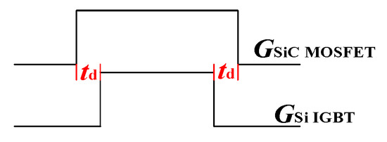
Figure 6.
Typical gate sequence control option of hybrid switch.
H. Liu et al. further studied the HT-ANPC topology using two HyS (E1-type) and four HyS (E2-type) [39,40,41,42]. In order to further reduce the switching losses, they proposed a hybrid modulation strategy [40]. Comparative analysis shows that the E1-type topology using two HyS is more suitable for high-power-density scenarios because its device junction temperature distribution range is narrower, and it is more advantageous in terms of efficiency and cost.
D. Jin et al. proposed the E3-type topology based on the B3-type topology, which considers both cost and loss, and applied HyS instead of SiC MOSFETs [43,44,45]. To further improve the efficiency of the inverter, they focused on the switching sequence of the HyS. In addition, P. Liu et al. proposed the E4/E5-type topology in [45] and comparatively analyzed all the topologies applying HyS. They further optimized the configuration algorithm of HyS in [44] to ensure that the performance of each switch is maximized. However, these comparison results are obtained in a simulation environment, and these data are not fully referable, but the general trend can still be seen on a macro level. Based on the performance comparison, among the E-type topologies, the E5-type topology has a higher efficiency for operation under a wide range of operating conditions. This is due to the fact that this topology utilizes parallel conduction paths to further optimize the conduction loss of the device and maintains the low switching loss of the device under different power factor conditions [45]. In addition, T. Xia et al. added an additional SiC Schottky Diode in parallel with the HyS to further reduce the reverse recovery loss of the HyS [46,47].
Compared with A-type and B-type topologies, the topologies applying HyS are proposed mainly due to the trade-off between the cost and loss of the system. But applying HyS increases the complexity of the system control. In addition, the probability of HyS failure is much higher than with the single-device application, which reduces the system reliability.
2.2.2. Miscellaneous Topologies
Regarding HT-ANPC topologies involving SiC devices, in addition to the above-mentioned single-phase topologies with six active devices, some researchers have also proposed several special topologies in order to further reduce losses and improve the switching performance of switching devices.
G1-type
For the A1-type topology, in order to reduce the reverse recovery losses of the body diodes, anti-parallel SiC Schottky diodes are selected outside the SiC MOSFETs. Although this reduces the overall losses to a certain extent, it will reduce the switching performance of the SiC MOSFETs. The structure with a split output can simultaneously reduce the conduction losses of SiC MOSFETs and influence its parasitic capacitances. S. Belkhode et al. earlier applied the structure with a split output to the HT-ANPC topology [48]. This topology not only reduces switching losses but also achieves optimal loss distribution and can operate under a wide range of power factors. The limitation of this topology is that the SiC MOSFETs cannot achieve complete decoupling, which will cause current circulation between two inductors.
G2-type
In view of the defects of current circulation in the two branches of the G1-type topology and considering the conduction losses of SiC MOSFETs, S. Belkhode et al. proposed the G2-type topology shown in Figure 5 [4]. This topology operates with high efficiency at high power density and minimizes the ground leakage current, so it is more suitable for transformerless photovoltaic applications.
The basic operating rules of this topology define the switching of Si devices and SiC devices at different timings, avoiding the occurrence of high short-circuit current and improving the reliability of stable system operation.
G3-type
The G3-type topology is similar to the G1-type topology but adds a high-frequency branch based on the split output structure. This topology was proposed earlier by M. Najjar et al. to apply low-current-level high-frequency switching device -SiC MOSFETs to reduce system costs and conduction losses of SiC MOSFETs [49,50].
Since the output side of this topology is a two-half-bridge interleaved structure, the switching timing of S2 and S7, S3 and S8 is the same, and they act as load current paths with positive and negative output levels, respectively.
However, an inevitable drawback of this topology is that the power of the two branches is unbalanced, and the additional balancing control also increases the control difficulty of the system.
G4-type
Similar to the G3-type topology, in order to meet the demands of high-capacity energy storage, C. Chen et al. proposed the HT-ANPC parallel structure [51,52]; this idea was earlier recommended by Infineon at PCIM2019 [53]. This structure allows a wider range of energy capacity of the system. It is worth noting that this type of modular parallel structure is not limited to two inverters. It can be extended to multiple inverters in parallel to achieve higher-rated power, higher reliability, and lower grid-side current harmonics. In addition, this type of parallel structure usually requires additional complex control due to the presence of zero-sequence circulating current.
2.3. GaN-Based Topologies
The earlier research on T-ANPC inverters involving all-GaN power devices was started for photovoltaic systems [18,19]. This type of topology has significant advantages in medium-voltage photovoltaic applications and also shows higher efficiency when operating at high frequency. However, the current research on GaN power devices is not mature enough, and poor thermal conductivity makes it difficult to apply them in high-power scenarios (GaN power devices have significant advantages in high-frequency applications of 10 kW and below). Therefore, there is currently a lack of research on HT-ANPC inverters involving GaN power devices, which mainly include the four topologies shown in Figure 7. GaN power devices operate at high frequency to achieve the normal output of the system, and their basic operating rules are similar to the A1-type topology. The F1-type topology was first proposed by G. Kapino et al. [54,55] and consists of Si MOSFETs and GaN FETs. The F2-type topology is similar to the G3-type topology, with multiple high-frequency output branches connected in parallel to achieve higher output power using low-current-stress switching devices [56,57,58]. The interleaved output structure of the high-frequency part of this topology reduces the output current ripple. In order to make the system have smaller overall losses, they used SJ MOSFETs instead of Si IGBTs for the two internal switching devices [56]. Furthermore, Y. Zhang et al. proposed a F4-type topology based on the study of losses in this type of inverter, which consists of 2Si and 4GaN switching devices. This topology is analyzed by simulation to achieve a better trade-off between cost and loss [57].
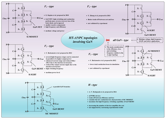
Figure 7.
Evolution of GaN-based HT-ANPC topologies.
As mentioned above, the obvious drawback of F-type topologies is that they are limited to small- and medium-power applications. For higher-power applications, a high-frequency branch applying GaN devices typically consists of multiple branches connected in parallel, increasing the number of devices and the cost.
H-type
In addition to the aforementioned hybrid topology of WBG devices and Si devices, A.V. Deshpande et al. proposed the H-type topology that mixed SiC MOSFETs and GaN HEMTs [59]. This topology maximizes the low-conduction-loss characteristic of SiC MOSFET and the high-frequency-switching capability of GaN HEMT. The different topologies have been analyzed by simulation comparison with practical devices, pointing out that the proposed topology achieves a trade-off between efficiency and loss, but the experimental results are unconvincing. Furthermore, in high-power applications, the H-type topology requires multiple high-frequency branches in parallel. This not only increases the number of devices in the system and the amplification cost but also adds complexity in terms of control. This topology defeats the initial purpose of establishing the hybrid topology, which is the trade-off between cost and performance.
2.4. Modulation Strategies
The basic operating rules of the above topologies are defined by different switching states, which are mainly divided into three operating states, including P, O, and N. The corresponding output levels are +UBus/2, 0, and—UBus/2, that is, three-level output. The O state provides a path for the load current to continue flowing. Some studies have also added different combinations of O switching states to achieve soft switching [26,29,30]. The realization of different switching states can be achieved through different modulation strategies, mainly including a carrier-based modulation (CBM) strategy and space vector modulation (SVM) strategy. The latter is more complex than the former, but the control freedom is also more flexible. CBM is usually combined with the research of zero crossing [60,61], dead zone mode [30,62], common-mode voltage elimination [63], and other issues. As for SVM, the optimization of its implementation method is currently a hot research topic [64,65,66,67,68]. There are also some other research hotspots, including the fault diagnosis and fault-tolerant control methods [69,70,71] and the neutral-point (NP) voltage balancing methods [72,73].
It is worth noting that, looking at the switching states of the inverter, the modulation strategies applied to HT-ANPC topologies are similar to the modulation strategies applied to T-ANPC topologies. As mentioned above, HT-ANPC topologies were proposed based on the consideration of the loss balance of devices and the system cost issue. This type of topology mainly concentrates on high-frequency operation on WBG power devices. Therefore, N. Prabaharan et al. conducted a detailed analysis of the modulation strategies applied in inverters from the perspective of low-frequency operation and high-frequency operation [74]. This part is not the focus of the review in this paper, so it will not be discussed in detail. In the above analysis of this paper, the current research hotspots of two types of modulation strategies are pointed out. Next, the differences between them and their respective application characteristics will be discussed.
- (1)
- CBM is the most basic modulation strategy. The biggest feature of it applied to HT-ANPC topologies is that the generated modulation signals are injected into the WBG power devices in a targeted manner. In the early experimental verification of the HT-ANPC topology or when the system does not need to add additional complex control for potential challenges, this modulation strategy is more suitable for simple open-loop verification of the proposed topology.
- (2)
- Compared with CBM, SVM is much more complex in the implementation, but the former is less flexible. The advantages of this modulation strategy are even more significant when additional controls need to be considered. Therefore, the application of the SVM strategy is often combined with the improvement of other issues.
- (3)
- In addition, for HT -NPC inverters, there are some additional modulation strategies based on the above two modulation strategies [55,63]. S.M. Maaz proposed the dynamic-phase-shift PWM (DPSPWM) strategy to attenuate common-mode voltage, while A. Kouchaki et al. chose to apply the third-harmonic-injection PWM (THIPWM) strategy to improve the quality of output power. Some researchers have also proposed hybrid modulation methods based on the above two modulation strategies. The hybrid modulation can refer to the combination of different modulation strategies as the carrier-based space vector modulation (CB-SVM) strategy [75,76]. It can also refer to the mixed application of different modulation strategies in the same system. For example, in order to reduce the losses of switching devices, H. Liu et al. proposed that the same topology should apply for different modulation strategies under normal operation and overload conditions [40]. Most studies use a modulation strategy based on a carrier comparison combined with additional control. This modulation strategy has a lower degree of control freedom but it is more convenient to apply and can significantly reduce the complexity of the system control. For example, H. Xu et al. investigated the problem of the limited control degree of freedom for hybrid topologies and proposed a multistep soft-switching modulation that utilizes multiple switching states to achieve the soft switching of all SiIGBTs [77].
2.5. Summary of Topology Derivation
The combination of HT-ANPC inverter topologies and the advantages and disadvantages of each type of topology are reviewed above. It is worth noting that the description and Figure 5 and Figure 7 indicate that the main considerations for the derivation of the various topologies include the system cost; the loss equalization distribution of the devices, i.e., the ability of the system to utilize the characteristics of the devices; and the power level. This subsection summarizes and discusses the topology level of HT-ANPC inverters and points out some issues in applications that facilitate the practical engineering applications of HT-ANPC inverters.
A detailed categorization of HT-ANPC inverter topologies has been presented in Table 2, which emphasizes the differences in WBG devices and identifies that the HT-ANPC inverter topologies mainly involve topologies involving SiC devices and topologies involving GaN devices. Among the topologies involving SiC devices, they are further categorized into regular topologies and miscellaneous topologies. Compared to the T-ANPC inverter topologies, the HT-ANPC inverter topologies optimally utilize the characteristics of each device, as well as the trade-off between system cost and performance.
- (1)
- Topologies involving SiC devices: These topologies are the most widely studied in the current research and include A-type topologies with two SiC MOSFETs, B-type topologies with four SiC MOSFETs, E-type topologies applying the hybrid switch consisting of a parallel connection of Si IGBT and SiC MOSFET (with SiC Schottky diode), and G-type topologies with an interleaved output structure or a parallel connection of high-frequency branches. Figure 5 exhibits the evolution path of these topologies.
The A1-type topology is the most popular research, which has a significant cost advantage and high flexibility of structure. However, this topology has the significant issue of voltage spikes at the switching moment of high-frequency devices. The parallel connection of multiple high-frequency branches in the A1-type topology forms the G3-type topology, which improves the power level of the system. In the A2-type topology, since the load current inevitably flows through the diodes connected anti-parallel with the Si IGBTs, the reverse recovery loss in this part decreases the performance of the system. In addition, due to the symmetric structure, Cell 2 and Cell 3 are usually applied with the half-bridge, or H-bridge, structure, which utilizes modular units to effectively increase the power density and reduce the influence of loop parasitic impedance.
The application of four SiC MOSFETs to the B-type topology fully utilizes the power performance of the device and improves the loss equalization issue. However, the cost is a concern, as SiC MOSFETs are much more expensive than Si IGBTs for the same voltage and current levels. Therefore, the power level of the system will also be limited by this type of device, and this effect is most significant for the B1-type topology. The E-type topology with hybrid devices has received much attention for several years. This device is mainly cost-conscious and enables the application of SiC MOSFETs with lower current ratings in hybrid devices, which also reduces the conduction loss at higher load currents. The complexity of the gate control sequence of this device class also reduces the reliability of the system. However, the trade-off between cost and performance should not be ignored.
The G-type topologies evolved from the regular topologies. The G1 and G2 topologies are studied mainly for photovoltaic application, utilizing parallel interleaved structures. The G3 and G4 topologies are similar for parallel applications. However, this type of topology has a similarity that there will always be power imbalance and circulating current between multiple branches.
- (2)
- Topologies involving GaN devices: Based on the comparison of Figure 5 and Figure 7, it can be seen that there is a lack of research on HT-ANPC inverters involving GaN devices, mainly due to the maturity of the current research on GaN devices as compared to SiC devices. GaN devices have lower voltage ratings and thus are not suitable for applications in high-power scenarios. However, similar to the G3-type topology, the F2-type and H-type topologies also apply multiple high-frequency branches to improve the power level of the system while also increasing the cost and control complexity of the system. For H-type, which is a hybrid topology with all WBG devices, the application of GaN devices enhances the overall switching frequency level, and both the loss issue and system performance are optimized. However, the feasibility of practical applications in industry has to be further investigated.
3. Potential Challenges and Improvements
HT-ANPC inverters face some potential challenges in various applications, which will directly or indirectly affect the loss, efficiency, reliability, etc., of the entire system and the number of devices in the topology, such as six active switches in a single-phase HT-ANPC topology and 18 active devices in a three-phase system. This will force focus on device damage and protection. At the same time, the quality of the output power is also a critical issue, especially for the grid-connected system. Since the load side of the inverter is connected to the grid, and the grid has high requirements for the ripple of the input voltage and current, it is worth studying to improve the output power quality of the front-stage inverter as much as possible. In addition, for the parallel application of multi-phase output branches and the parallel application of inverters, there are also problems of the current imbalance and circulating current. These issues have also been discussed at the end of the previous section, and this section follows with a comparative analysis of these potential challenges and current enhancements.
3.1. Devices
The high frequency and the high efficiency in energy storage systems and electric propulsion systems place increasingly high demands on switching devices [6,7,78]. Compared with issues such as efficiency and cost, the stable operation of the inverter is the primary factor that should be considered when designing a system application. It should be noted that the damage to the switching device will cause tremendous damage to the entire system. Compared with the T-ANPC topology, the combination of different types of switching devices in the HT-ANPC topology itself is a safety hazard for the operation of the system because their switching characteristics and operating frequencies are very different. Therefore, many papers are focusing on protecting switching devices in the HT-ANPC topology.
3.1.1. Open-Circuit Fault
Switching device faults are generally divided into two types: the open-circuit fault and the short-circuit fault. The short-circuit fault typically produces abnormal overcurrent, causing damage to other parts of the system. When a short-circuit fault occurs, the system operation should be interrupted in time, and the location of the fault should be checked and repaired in time. Hence, most of the research focuses on the open-circuit fault of switching devices, involving fault detection methods and fault-tolerant control methods.
K.-B. Lee et al. analyzed the impact of a switch fault on the system [79] and proposed corresponding detection methods in [9,62,69,80,81,82]. When an open-circuit fault occurs in a device in the topology, the waveform of the load current will be distorted. Therefore, the research team proposed detecting the location of the fault based on the current distortion [62,80]. They used the waveform of the output current when the system is operating normally as a reference, as shown in Figure 8. The waveform is the current id and iq on the d-q coordinate axis, defined by Equations (1) and (2) [9].

Figure 8.
Typical output current pattern under healthy condition of HT-ANPC topology.
The disadvantage of this method is that similar distorted current waveforms will appear when switching devices at different locations fail, and the exact location of the fault cannot be distinguished. In order to improve it, a method of using zero-switching states to identify faults was proposed [62]. However, this method strongly depends on the level of output current, and the application of additional zero-switching states increases the complexity of the system.
Based on the above problems, a method for automatically extracting current characteristics using deep learning was proposed in [81]. This method is based on the Convolution Neural Networks (CNNs) algorithm and can be used to detect the exact location of system faults at various current levels. Similarly, S. Belkhode et al. proposed a method for diagnosing and detecting switch faults using Siamese Neural Network (SNN) technology [83]. Applying these deep learning technologies provides a new idea for future research on this topic.
r2 = Ids2 + Iqs2
θ = tan−1(Iqs,cen/Ids,cen)
Based on the above fault detection methods, a series of fault-tolerant control methods have been proposed [69,70,82,84,85]. Y.-J. Kim et al. proposed a method of replacing two zero-switching states with each other [82]. This will increase the losses of adjacent Si IGBTs and their anti-parallel diodes. Therefore, H.-R. Jo et al. improved it [85] and reduced the switching losses. The total harmonic distortion (THD) of the output current was enhanced when the output current level was high. But this method increases the complexity of the system control to a certain extent.
K.-B. Lee et al. have comprehensively analyzed the fault-tolerant control method for switch faults in the HT-ANPC topology based on the SVM strategy [69]. The reference voltage of each phase is recalculated, and the action vector of each sector is redistributed. This method does not add additional hardware circuits or change the system structure. They conducted a more detailed analysis in [71]. However, applying additional switching states in the event of a system fault will bring additional burdens to the control of the system. The above methods are compared in Table 3.
Table 3.
Comparison of fault diagnosis and tolerant control methods.
3.1.2. Over-Voltage Risk
For the HT-ANPC topology, over-voltage is mainly analyzed at the turn-off time of high-frequency switching devices [13,86]. It is also called the voltage spike. Taking SiC MOSFET as an example, the drain-source voltage spike during turn-off is mainly affected by the parasitic inductance of the loop and the turn-off speed of the switching device. If the turn-off speed is reduced, its switching losses will increase. Therefore, most research focuses on optimizing the switching states to minimize the commutation path and reduce the over-voltage risk [29].
As mentioned above, an excessively long commutation path is the dominant factor causing voltage spikes. Therefore, some studies have also reduced the voltage stress of the switching device by decoupling the commutation path to reduce the parasitic inductance of the loop [56,60,87]. A common method is to connect a decoupling capacitor in parallel before the high-frequency branch, which is the HT-ANPC with a decoupling capacitor (HDT-ANPC) topology, as mentioned above. This application was formally proposed in [7], as shown in Figure 9. It can be seen that the decoupling capacitor divides the commutation loop of the high-frequency switching device into two small loops. However, adding a decoupling capacitor also brings adverse effects: the generation of inrush current when the system is commutated at the fundamental frequency and the occurrence of resonance in the loop when switching high-frequency devices [22,86,88]. This will increase the risk of damage to low-frequency switching devices. So, some researchers have proposed corresponding suppression methods for the above two problems. This paper summarizes them in Table 4.

Figure 9.
Typical diagram of the HDT-ANPC topology.
Table 4.
Comparison of suppressing methods for negative impacts of the decoupling capacitor on HDT-ANPC topology.
In addition, based on the above two methods for reducing the over-voltage risk, this paper provides a comparative analysis in Table 5, which helps researchers to see their advantages and disadvantages more clearly.
Table 5.
Comparison of suppressing methods to reduce the over-voltage risk.
3.2. Low Output Power Quality
There are many factors that affect the output power quality of HT-ANPC inverters. This paper analyzes several vital challenges. These include voltage imbalance at the neutral point, harmonic elimination of the output side, electromagnetic interference (EMI), and zero-crossing voltage distortion. Among them, the NP voltage imbalance will make the output sinusoidal voltage asymmetric, and the harmonic components of the output side will directly affect the reactive power of the system. Especially for grid-connected systems, harmonic injection into the grid will reduce the power factor of the system. EMI will further aggravate the harmonic components on the output side, and the interference will also have a negative impact on the regular operation of other equipment in the system. Moreover, zero-crossing distortion will cause an additional voltage spike when the output voltage crosses zero, reducing the output power quality. Therefore, this paper analyzes the above main aspects of output power quality in this subsection.
3.2.1. Imbalance of Neutral-Point (NP) Voltage
In the real operation of the system, unreasonable switching states, excessive stray impedances in the commutation loop, and the presence of loads will lead to an imbalance in the half-bus voltage on the DC side. This problem affects the output power quality and the loss balance of the switching devices. Therefore, the NP voltage balance is a particularly important issue in T-NPC, T-ANPC, and HT-ANPC topologies.
K.V. Vilerá et al. systematically analyzed the NP voltage problem of the T-ANPC topology based on the SVM strategy [72]. C. Li et al. optimized the modulation strategy based on the particularity of the HT-ANPC topology [25]. By injecting different voltage vectors, complex control problems such as NP voltage balance and zero-sequence common-mode voltage modulation were solved. In addition, K.-B. Lee et al. changed the small-acting vector to improve the imbalance of NP voltage [64,75]. The specific approach is to replace the voltage vector that will generate significant current harmonics with two voltage vectors in opposite directions. However, the above two methods have a common constraint that when the reference voltage vector is using different small sectors, all voltage vectors cannot be applied, including small vectors and zero vectors. This constraint will affect the voltage balancing effect. M. Najjar et al. improved the above method [73]. The small and large sectors were further divided, and the acting vector was reasonably selected. The application of the improved modulation strategy can eliminate the voltage ripple to a large extent and effectively control the NP voltage.
There are some other control methods [6,65,66,90,91], where the main idea is to combine the model predictive control method to improve the problem of NP voltage imbalance. M. Novak et al. applied the finite-set model predictive control (FS-MPC) algorithm to the HT-ANPC topology earlier [91]. The algorithm uses an artificial neural network to determine the optimal weight factor in the cost function [90]. The balancing effect of this method strongly depends on the weighting factor of flux error in the cost function. Hence, D. Xiao et al. implemented the NP voltage balance problem and other control objectives through two independent predictive optimization loops, eliminating the influence of the weight factors [66]. However, the algorithm requires more enumeration to determine the optimal solution, increasing the complexity. Z. Sun et al. proposed a new model predictive control algorithm based on it [65]. The algorithm implemented multiple objectives in stages, reduced losses, and improved the control performance.
In addition, X. Xu, H. Chen, and others provided different ideas for the NP voltage balancing method of complex systems [6,51]. Based on different structures, they specifically combined the advantages of their own topologies and proposed a relatively unique control method. This paper also provides a comparison of NP voltage balancing methods in Table 6.
Table 6.
Comparison of suppressing methods to balance NP voltage.
3.2.2. Harmonic Distortion
In practical applications, the nonlinear switching process of the switching device and the modulation strategy applied will affect the harmonic components on the inverter output side to varying degrees. The harmonics of the inverter will generate EMI and affect the regular operation of other surrounding systems. Therefore, appropriate harmonic processing measures need to be taken to reduce the impact of harmonics.
At present, the main methods for reducing the harmonic components of the inverter can be divided into software and hardware. The software aspect is to reduce the harmonic components by optimizing the modulation strategy and control methods [25,54,76]. C. Li et al. analyzed the output harmonic problem of the HT-ANPC inverter earlier [25]. Based on the SVM strategy, the switching states were optimized to achieve lower output THD. G. Kapino et al. optimized the CBM strategy to reduce harmonics [54]. The dead time was increased in the switching process of the switching device, and the PWM wave was quickly and accurately implemented using the field programmable gate array (FPGA), avoiding the shoot-through issue of the inverter. S. Belkhode et al. combined the above two methods and proposed a CB-SVM strategy, which improved the efficiency and harmonic performance of the inverter [76]. This paper will compare the above typical software implementation methods in Table 7.
Table 7.
Comparison of harmonic suppression methods.
Additionally, in order to attenuate the harmonic components on the inverter output side, a more convenient and mainstream hardware implementation method is to add an extra passive filter [84]. However, if the design is unreasonable, the existence of the filter will also bring more burden to the system. Therefore, the design of the filter has received more and more attention.
The filter design should mainly consider structure selection, parameter calculation, and volume optimization. The more effective and common filter structure is the second-order single-stage LC filter. A. Kouchaki et al. conducted a detailed analysis of the filter design for an inverter system composed of all GaN HEMTs [18]. The parameter selection of passive components in the filter was derived. The reference criteria were as follows:
- (1)
- To provide sufficient damping at the switching frequency and keep the resonant frequency away from the inverter switching frequency, the required attenuation was selected as 0.01.
- (2)
- The output ripple current was selected as 20% of the peak output current to limit the switching current of the maximum power device and keep the inverter output current ripple at a reasonable level.
In addition to the LC filter above-mentioned methods, common filters in inverter systems include L, RC, RLC, and LCL filters. Among them, the LCL filter has received increasing attention due to its small size and low cost [84]. For HT-ANPC inverters, LCL filters are also applied in [7,19,21,32,67,92] to improve the quality of output power.
In addition to those mentioned above, unilateral harmonic suppression, M. Li and Z. Cai et al. improved the modulation strategy while adding a filter [60,89]. This further reduced the harmonic components on the output side. Based on the above analysis, this paper compares typical harmonic suppression methods, as shown in Table 7.
3.2.3. EMI
For hybrid topologies, the application of WBG power devices has dramatically improved efficiency and power density. On the other hand, the high switching frequency, du/dt, and di/dt lead to a significant increase in the harmonic components of the noise source and changes in the impedance network. This increases the conducted interference and reduces the quality of the output power. It will also cause unintentional EMI to other nearby systems during operation. There are existing papers that perform a comprehensive analysis of the EMI issue of WBG power devices [93], so this paper mainly discusses the EMI issue based on the HT-ANPC topology.
Conducted interference mainly includes common-mode noise and differential-mode noise. Between them, the interference of electrical equipment to the outside is primarily common-mode noise, and the external interference is also mainly common-mode noise. It is related to the parasitic inductance and package inductance of the PCB layout [89]. Therefore, some researchers have reduced the EMI by optimizing the PCB layout [19]. In addition, there are also some studies similar to the above-mentioned harmonic suppression method to mitigate interference by adding the EMI filter. Within a particular switching frequency range, EMI standards are more stringent than harmonic standards. Hence, J. Wang et al. conducted a detailed analysis of the design of the filter [5,89,94]. They pointed out that increasing the order of the EMI filter can better attenuate both common-mode noise and differential-mode noise, but blindly increasing the order will also reduce the power and efficiency of the system. After comprehensive consideration, A. Kouchaki et al. chose to apply a third-order filter [89] and conducted a detailed analysis of the selection of components. However, this approach is not advantageous in terms of volume and cost.
In order to further reduce common-mode noise, D. Zhang et al. applied neutral-line-return suppression, i.e., the neutral point is connected to the midpoint of the DC bus [5]. Nevertheless, this method requires the establishment of an accurate common-mode model. The simple model is not exact and is prone to causing significant deviations in the measured results. Based on the above problems, J. Wang et al. conducted a detailed analysis [92,95]. An impedance balance suppression method was proposed. This method adds additional inductance to the loop by applying the neutral line return. The parameter design of the inductance and capacitance was analyzed in detail, and the influence of the circulation of the loop current was considered. By comparison, it can be seen that this reported suppression method has more advantages: better suppression effect, smaller cost and volume, and medium-circuit common-mode impedance. Their research has a specific reference value in practical engineering applications. Furthermore, interesting work has been conducted by Y. Yu et al. They addressed the multi-source EMI problem in PV inverters by first proposing a decoupling method and then a targeted suppression strategy for the single-source EMI problem. They contributed to the study of EMI suppression in multi-converter systems [96].
In addition, some researchers have proposed attenuating common-mode interference by optimizing modulation strategies [63,64,65,66,67,68,69,70,71,72,73,74,75]. S.S. Hakami et al. optimized the CB-SVM strategy and created a new switching scheme by selecting the voltage vector with the least impact on the DC link current ripple according to each sector [75]. The common-mode voltage is significantly reduced. However, an important disadvantage of this method is the increase in switching losses. Therefore, S.M. Maaz et al. proposed a DPSPWM strategy that reduced the common-mode voltage, switching losses, and harmonic components [63]. Similarly, a comparison of EMI suppression methods is shown in Table 8.
Table 8.
Comparison of EMI suppression methods.
3.2.4. Zero-Crossing Distortion
During the regular operation of the HT-ANPC inverter, the switching process of the low-frequency switching devices is named zero crossing. In this process, high-frequency switching devices often generate abnormal voltage due to improper switching behavior [60]. This abnormal voltage refers to the instantaneous pulse generated at the zero-crossing point where the output pole voltage polarity changes. It causes current distortion and must be removed. Analysis shows that the difference in the switching time of different switching devices is the root cause of the voltage anomaly. Therefore, J. He et al. eliminated the abnormal voltage by improving the switching state [26,60,61]. The main idea of these methods is to clamp the output voltage of the inverter to the midpoint of the DC link at zero crossing to improve the output voltage characteristics.
3.3. Other Challenges
3.3.1. Power Unbalancing
The multi-output structure was presented to handle higher power levels. A typical approach is to add high-frequency branches. Taking the typical G2-type topology shown in Figure 5 as an example, a high-frequency branch is added to form an interlaced structure [49]. This unique topology helps to reduce the losses in the high-frequency switching devices. In addition, similar multi-output structures can adopt the method of connecting multiple high-frequency half-bridges in parallel [56]. This helps to improve the current carrying capacity of high-frequency switching devices while also increasing the output power and reducing the filter consumption. However, the disadvantage of this application is that it is difficult to control, and there will be current deviations between the bridge branches, resulting in an uneven load distribution and causing the switching devices in the highest power branch to be destroyed first. Therefore, C. Beckemeier et al. dynamically adjusted the switching frequency of the switching devices in each bridge for the inverter structure with six high-frequency bridge branches [58]. While reducing the control difficulties, the current balance between the bridge branches is effectively achieved.
3.3.2. Circulating Current
In the case of high-power energy storage requirements, the rated power of a single HT-ANPC inverter is limited, so a modular parallel approach is often used to increase the overall power level of the system [63]. As mentioned above, in parallel structure like the G4-type, since the topology shares the DC and AC bus, the problem of zero-sequence circulating current will be introduced [97]. This circulating current will cause harmonics and reduce the efficiency of the system. H. Chen et al. conducted a detailed analysis based on the zero-sequence circulating current model in the HT-ANPC inverter parallel structure. They proposed a coordinated control strategy for zero-sequence circulating current and NP voltage [51]. The mutual influence between these two issues was not considered further. So, they further focused on analyzing it in [98]. The SVM-based model of both was provided, and they were suppressed by adjusting the duration of the redundant small vector without significantly affecting each other. Based on this, they further studied and improved the adaptability of the coordinated control strategy [52].
The summary of this section is shown in Table 9.
Table 9.
Summary of potential challenges and improvements in applications.
4. Comparison and Discussion of Various HT-ANPC Inverters
In order to provide a more comprehensive overview of HT-ANPC inverters, this paper will compare and discuss typical topologies in detail, as shown in Table 10, focusing on cost, research status, and performance. In addition, at the end of this section, this paper states the steps and processes for the broad design of topologies in different scenarios.
Table 10.
Performance comparison of typical HT-ANPC topologies.
4.1. Cost
As shown in Table 1, for switching devices of the equivalent level, SiC MOSFET and GaN FET/HEMT are much higher in cost than Si IGBT. Compared with the T-ANPC inverter composed of all-SiC MOSFETs or GaN FET/HEMTs, the HT-ANPC topology combines switching devices of different material types according to specific switching frequency requirements and should have advantages in terms of cost.
As illustrated in Table 10, the cost evaluation can be preliminarily assessed based on the number of WBG power devices. However, this study does not investigate other system components beyond the topology itself, since the proposed hybrid topology is primarily due to the trade-off between performance and the cost of the topology itself (mainly active switching devices are considered).
In this paper, the cost issue has been emphasized many times. For a system, the cost factors mainly include material and production costs. For more complex inverter systems such as the HT-ANPC topology, the cost issue will be more critical. This is because for three-level inverters and even higher-level inverter systems, the number of switching devices is more than that of two-level converters, and the power level is also higher. The selection of more components, including filters on the input and output sides and circuits on the drive side, is more stringent.
4.2. Research Status
Based on the referenced literature, this paper briefly summarizes the relevant research papers of various topologies, as shown in Figure 10 and Figure 11. It can be seen that the research on HT-ANPC topologies involving SiC devices is more extensive nowadays, especially the A1-type topology containing two SiC MOSFETs and the B1-type topology containing four SiC MOSFETs. The topologies involving GaN devices need to be further studied because they have more uncertain factors.
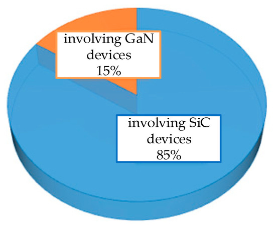
Figure 10.
Percentage of different material type devices in papers.

Figure 11.
Number of papers on HT-ANPC topologies.
4.3. Performance
This paper compares the performance of various typical topologies through various indicators and summarizes them clearly in Table 10. The data listed in this table are determined based on the corresponding references. However, in most of the literature, the used simulation parameters are different from the experimentally verified ones [21,50]. Therefore, the results summarized in this paper are based on specific working conditions.
It is worth noting that each comparison table summarized in this paper is based on comparisons concluded from the papers’ description of the system design. For example, in the comparison of complexity, metrics such as the hardware design of the system, the modulation strategy, the additional control, and the additional requirements are considered.
4.3.1. THD
For HT-ANPC inverters, the output voltage is not a pure sine wave because it contains harmonic components. In the literature, THD is often used to evaluate output power quality. This factor represents the degree of closeness of the measured waveform to its fundamental wave and is defined as the root of the sum of the square of all the harmonics above the fundamental divided by the RMS value of the fundamental. According to the IEEE 519 standard (IEEE Standard for Harmonic Control in Electric Power Systems, Published on 5 August 2022 by US-IEEE), the limit values of THD under different voltage-level applications are shown in Table 11 [74].
Table 11.
IEEE 519 standard for THD.
This factor can reflect the quality of the output power. According to the THD values listed in Table 10 (these values are the actual measured results under a specific modulation ratio, and some papers do not mention them), it can be seen that THD is often reduced by adding additional designs, including filter design, modulation strategy, NP voltage imbalance control, etc. [5,25,55].
4.3.2. Efficiency
When evaluating a topology or even a system, efficiency is the most important. In the inverter system, it represents the ratio of the input DC power to the output AC power. Its calculation can simply be defined as the ratio of output power to input power. This factor includes the losses of the system in the process of converting power. The cost utilization rate from this factor also can be seen using lower costs and lower system complexity to achieve efficient operation of the system. This is the goal during a design process.
The losses of the inverter seriously affect the efficiency of the entire system. One of the key points of the HT-ANPC topology, when it was first proposed, was to reduce the overall loss to improve the efficiency. This mainly includes the switching losses and conduction losses of the switching devices and the reverse recovery losses of the anti-parallel diodes of the active devices. S. Belkhode and other scholars have conducted a detailed analysis of the system loss [4,21,30,31,76]. From this, the efficiency of the system can be reversely calculated.
The efficiency of various typical topologies listed in the table is based on the measured data in the paper and the DC bus voltage level. In order to discuss the performance of the topologies more accurately, the efficiency results listed are based on real experiments measured. Some conference literature has been analyzed by simulation only for the proposed topologies, and this review does not refer to these data, which lack practical significance. From the measured efficiencies listed in Table 11, it can be seen that in regular topologies, when the voltage level is higher, the efficiency of the topologies involving SiC MOSFETs will be larger. Among them, the B1-type topology containing four SiC MOSFETs is more advantageous [5]. Topologies involving GaN devices are more widely used in medium-voltage and medium-power scenarios [56]. Since GaN devices are still developing, the performance of the corresponding topologies can be further studied and verified. In addition, although several special topologies have advantages, such as short-circuit fault tolerance, the additional devices have not brought significant improvements to the efficiency of the system [4,48,49,50]. It is worth noting that under different voltages, power levels, and additional control methods, the performance of the system cannot be evaluated simply from an efficiency point of view. And the development of material is still ongoing, so it cannot be generalized yet.
4.3.3. Power Density
Power density and efficiency are closely linked. The power density of the HT-ANPC inverter system can be defined simply as the ratio of the input power to the inverter volume. In recent years, in order to reduce carbon emissions and save energy, the design of inverters has constantly pursued higher power density [5,28,33,50]. The benefits of a high-power density design for the system are not only reduced volume and weight but also lower material costs. In addition, the realization of high power density requires consideration of the selection of the topology and its modulation strategy, reasonable PCB layout, and an optimal application of board materials to achieve better system thermal performance.
In the discussion of power density for inverter topologies, power density is typically evaluated using two metrics: power per unit volume (kW/dm3) and power per unit mass (kW/kg). For power per unit volume, the value of power density can be estimated by the ratio of the input power to the total system volume. The power per unit mass can be calculated in the same way. It can be seen that the calculation of power density is simpler, but the definitions of input power and volume in power density calculations are ambiguous, and they are affected by a variety of factors, such as ambient temperature, PCB layout, component parameters, additional hardware requirements, etc. However, we can inversely compare the power density of different systems because the value is inversely proportional to the number and size of devices. Taking TI’s reference design as an example, a conventional operating system consists of the following: switching device (ns) and driver (ndr), passive component (np), bias power supply (nvs), control board (ncb), sensing electronics (nse), filter (nfi), and heatsink (nsi) [99]. Based on this, we reflect the power density through the volume factor (βin) of the system, which can be defined as:
βin = Σnx × γx
The number of switching devices includes the diodes in the anti-parallel of the controllable devices, and the passive components mainly refer to capacitors and inductors. Assuming that the number of heat sinks is equal to the number of switching devices, the number of bias power supplies is approximated to be estimated as the sum of two times the number of drivers and the number of control boards. There are ns = nsi, nvs =2 ndr + ncb. Moreover, based on the volume relationship between the equipment, the volume coefficients (γx) of each piece of equipment can be defined as follows: γs = γsi = {1,5/6,1/2,1/6} × {2/3,1/3} (depending on the degree of device integration and the number of WBG devices), γdr = γcb = 2, γp = 4, γvs = 3, γse = 1, γfi = 1,2/3,1/3. Finally, the βin defining the power density of the single-phase HT-ANPC inverter system is calculated as a comparison criterion: high (≤70), medium (71~99), low (≥100).
On the basis of this criterion, this paper compares the results of the power density assessment of each inverter system displayed in Table 10; for the literature, there are power density specific calculation results excluded. It can be seen that the topology system for integrated applications has a higher power density, and the design of filters, heat sinks, and other related designs also affect the power density rating of the system. Taking reference [41] as an example, H. Liu et al. applied a half-bridge module and optimized the size of the switching device chip and the design of the heat sink to improve the power density of the system and at the same time achieved efficient operation of the system.
4.3.4. Junction Temperature
Different types of HT-ANPC topologies and appropriate modulation strategies can improve the problem of uneven device losses. An important indicator that reflects the uneven losses of switching devices is their junction temperature. Paying attention to the junction temperature of devices is to prevent them from being irreversibly damaged. During system operation, the switching state of the topology can be adjusted according to the junction temperature of the device, and appropriate heat dissipation structures can be added to extend the life of the switching device and increase the reliability.
4.3.5. Rated Power Operation (RPO)
As we know, the operating point of a system modeled through a simulation is full of uncertainties. Therefore, this factor aims to confirm the credibility of the data reported in the literature and to assess the accuracy of the performance of topologies. The HT-ANPC topologies whose RPO capability has been experimentally verified are summarized in Table 10, and it can be seen that there are still some HT-ANPC inverter topologies with different rated design specifications that need to be further investigated to ensure that they can be applied in practical industrial applications.
4.4. The Selection Procedure of the Specific Application Topology
A complete HT-ANPC inverter system should include the main power circuit, drive circuit, sampling circuit, etc. The specific ones to be considered mainly include (1) selection of active switching devices, driving chips, controllers, and switching relays; (2) filter design and device selection; (3) sampling circuit design and sensor electronic device selection; (4) isolated bias power supply and auxiliary power supply design; (5) loop layout and circuit board design; and (6) thermal management.
As shown in Figure 12, the first step is to determine the appropriate topology type based on the application scenario and voltage level. Then, the system design needs to be carried out. This includes the selection of switching devices, PCB layout, filter design, and adding additional control for potential challenges in the topology. The factors that need to be considered are listed in Figure 12. Subsequently, various performance evaluations are performed on the topology, including junction temperature, THD, power density, efficiency, cost, etc. The selection of the inverter topology is based on the actual application requirements.

Figure 12.
Selection process of the HT-ANPC topologies from system to component.
Based on the mentioned above review of HT-ANPC inverters, the following three points that should be considered in the application of HT-ANPC inverters are pointed out.
- (1)
- Efficiency of system operation: In different application scenarios, the topology and modulation strategy should be reasonably selected. In addition, in order to minimize the interference of stray impedance in the loop, the PCB layout of the device should be taken seriously.
- (2)
- Reliability of system operation: Since the damage to switching devices has a significant impact on the system, the switch faults that may occur during the operation of the power converter should be predicted. The corresponding detection and fault-tolerant control methods should be reasonably applied to ensure the system can operate safely and stably.
- (3)
- Quality of system output power: improve the quality of output power, including the reasonable design of the heat sink, electromagnetic interference, filter, etc.
5. Future Prospects
The rapid development and maturity of power electronic devices and WBG power devices has made HT-ANPC inverters widely used in various industrial scenarios. This has attracted the attention of many researchers to the HT-ANPC topology. This paper conducts a study of HT-ANPC inverters to give researchers a better understanding of them. Based on the literature review and the current blind spots in the research, future research trends are discussed on this topic as follows.
5.1. Power Module Application and Its Packaging, Layout Technology
In order to achieve the higher power density of the system, modular integrated applications are gaining more and more attention [7,19,56,87,89,100]. This application includes partial inheritance and full integration. Partial inheritance means that the topology consists of half- or full-bridge module and discrete devices [7,30,31], while full inheritance refers to the application of the power module [47,87]. The main problem of this type of application is minimizing the stray inductance in the loop. This is because the loop layout will significantly affect the conduction interference, increase the losses, and reduce the efficiency. This is especially true for the HDT-ANPC topology. The external decoupling capacitor will increase the stray inductance of the loop and significantly reduce the suppression effect of the voltage spike. Therefore, how to design the module structure and optimize the loop will continue to require attention in the future [101,102]. In addition, the differences in hybrid device chips increase the rigor of the layout. At the same time, the heat dissipation performance of the module must also be taken into account. It requires that the module packaging be designed reasonably, including the substrate and package design, involving the application of materials science and mechanics.
5.2. Device Integration Technology
From the above analysis, it can be seen that some researchers have applied different devices in parallel in topological structures [37,38,39,40,41,42,43,44,45,46]. However, there are few studies involving the application of multiple devices in series and parallel. Reasonable parallel connection of multiple switching devices can reduce the current stress of each switching device and significantly improve the heating problem. As is known, the damage caused by switching devices can be attributed to the problem of heat because the damage caused is irreversible. This application should also consider the current sharing problem of switching devices. Current sharing is a critical issue in the application of devices in parallel connection because uneven current sharing can easily cause the switching devices to be damaged one after another. Moreover, applying multiple devices in series is also a popular topic in current topological structures. The voltage imbalance of the switching devices is the main problem of this application, and a reasonable design of the driver is even more critical in the application of switching devices in series.
5.3. Bidirectional Isolated DC/DC Converter
Currently, the application of MLIs in DC/DC converters is mainly concentrated in the dual active bridge (DAB) isolated converters. DAB converters are widely used in various fields due to their advantages, such as better electrical isolation, high power density, bidirectional power flow, easy soft switching, and higher voltage levels. The application of multilevel converters can significantly reduce the voltage stress of the switching devices and improve the performance of the converter [103]. At present, for the application of high-voltage DAB converters, the research on multilevel topologies is mainly focused on three-level and five-level circuits [103,104,105]. However, there are not many studies on topologies containing hybrid material devices in DAB applications, but the application of hybrid material devices has become a trend in the research of multilevel circuits. It can achieve high efficiency while keeping the system cost low [101]. Therefore, the application of HT-ANPC topology in DAB converters can focus on the performance comparison of different types of topologies, the soft-switching implementation of the specific topology, and the optimized design of the transformer to improve system efficiency.
6. Conclusions
The rapid growth of WBG power devices has spurred the development of the HT-ANPC inverter. This paper mainly focuses on classifying recent HT-ANPC topologies in terms of device materials. The main contributions are as follows.
- (1)
- Classification and evolution of HT-ANPC topologies: according to the material types of the devices, this paper comprehensively classifies the HT-ANPC topologies and summarizes their evolution.
- (2)
- Analysis of challenges and improvements: It provides a comprehensive analysis of the potential challenges of HT-ANPC topologies in applications. It then presents a comparative analysis of current reported improvements regarding various major challenges.
- (3)
- Comprehensive performance comparison of HT-ANPC inverters: According to the main evaluation factors of the HT-ANPC inverters, this paper conducts a comprehensive analysis of various topologies, including their performance, research status, etc. In addition, it briefly summarizes the selection and design process of topologies for specific application scenarios and indicates important design points that should be focused on in the application.
- (4)
- Key future trends of HT-ANPC inverters: it discusses the future development trends of the HT-ANPC inverter.
Based on the analysis in this paper, the following three recommendations can be given.
- (1)
- In high-frequency and high-power applications, topologies involving SiC devices should be given priority. Topologies involving GaN devices should be given priority in high-frequency and medium–low-voltage applications. If the application has high requirements for power density, the B-type HT-ANPC topologies should be given priority.
- (2)
- The performance improvement methods of each part should consist of the following: reduce additional control, avoid adding devices, and reduce the increase in system cost and volume.
- (3)
- Temperature-monitoring equipment can be added to avoid irreversible thermal damage to switching devices.
Author Contributions
Conceptualization, W.W., F.B., X.M., H.C., X.W., and H.W.; methodology, H.C.; software, X.W.; validation, H.C.; formal analysis, X.M., W.W., H.C., H.W., and F.B.; investigation, H.C.; resources, X.M. and W.W.; data curation, H.C.; writing—original draft preparation, H.C., W.W., and H.W.; writing—review and editing, X.M., W.W., H.C., H.W., L.Y., H.S.-H.C., and F.B.; visualization, H.C.; supervision, W.W.; project administration, X.M. and W.W. All authors have read and agreed to the published version of the manuscript.
Funding
This study is supported by the State Key Laboratory of Advanced Power Transmission Technology (Grant No. GEIRI-SKL-2023-003).
Data Availability Statement
The original contributions presented in this study are included in the article. Further inquiries can be directed to the corresponding authors.
Conflicts of Interest
The authors declare no conflicts of interest.
Abbreviations
The following abbreviations are used in this manuscript:
| WBG | Wide bandgap |
| T-ANPC | Three-level active neutral-point clamped |
| HT-ANPC | Hybrid T-ANPC |
| MLI | Multilevel inverter |
| VSI | Voltage source inverter |
| CSI | Current source inverter |
| T-TNPC | T-Type neutral-point clamped |
| T-NPC | Diode neutral-point clamped |
| VGC | Voltage generation cell |
| SNC | Lf selection network cell |
| CSC | Hf commutation switch cell |
| CBM | Carrier-based modulation |
| SVM | Space vector modulation |
| NP | Neutral point |
| DPSPWM | Dynamic phase-shift PWM |
| THIPWM | Third-harmonic injection PWM |
| CB-SVM | Carrier-based space vector modulation |
| id, iq | Current on the d-q coordinate axis |
| CNNs | Convolution neural networks |
| SNN | Siamese neural network |
| THD | Total harmonic distortion |
| HDT-ANPC | HT-ANPC with a decoupling capacitor |
| Cdec | Decoupling capacitor |
| EMI | Electromagnetic interference |
| FS-MPC | Finite-set model predictive control |
| FPGA | Field programmable gate array |
| Udc | DC bus voltage |
| DAB | Dual active bridge |
References
- Wang, J.; Peng, F.Z. Unified power flow controller using the cascade multilevel inverter. IEEE Trans. Power Electron. 2004, 19, 1077–1084. [Google Scholar] [CrossRef]
- Rodriguez, J.; Bernet, S.; Steimer, P.K.; Lizama, I.E. A Survey on Neutral-Point-Clamped Inverters. IEEE Trans. Ind. Electron. 2010, 57, 2219–2230. [Google Scholar] [CrossRef]
- Belkhode, S.; Shukla, A.; Doolla, S. Analysis of antiparallel diode connection for hybrid Si/SiC-based ANPC for PV applications. In Proceedings of the 2019 IEEE Energy Conversion Congress and Exposition, Baltimore, MD, USA, 29 September–3 October 2019; pp. 1905–1910. [Google Scholar]
- Belkhode, S.; Shahane, R.; Shukla, A.; Wang, J. A Split-Phase Enhanced Hybrid Active NPC Topology for PV Applications with Short-circuit Fault Tolerant Capability. In Proceedings of the 2022 IEEE Energy Conversion Congress and Exposition, Detroit, MI, USA, 9–13 October 2022; pp. 1–7. [Google Scholar]
- Zhang, D.; He, J.; Pan, D. A Megawatt-Scale Medium-Voltage High-Efficiency High Power Density “SiC+Si” Hybrid Three-Level ANPC Inverter for Aircraft Hybrid-Electric Propulsion Systems. IEEE Trans. Ind. Appl. 2019, 55, 5971–5980. [Google Scholar] [CrossRef]
- Xu, X.; Liu, N.; Wang, K.; Zheng, Z.; Li, Y. Modulation and Control of an ANPC/H-Bridge Hybrid Inverter for Ship Electric Propulsion Drives. In Proceedings of the 2019 22nd International Conference on Electrical Machines and Systems (ICEMS), Harbin, China, 11–14 August 2019; pp. 1–5. [Google Scholar]
- Beye, M.L.; Bimmel, L.; Bier, A.; Martin, J. Multilayer busbars for medium voltage ANPC converter dedicated to battery energy storage systems. In Proceedings of the 2022 24th European Conference on Power Electronics and Applications (EPE’22 ECCE Europe), Hanover, Germany, 5–9 September 2022; pp. 1–8. [Google Scholar]
- Gurpinar, E.; De, D.; Castellazzi, A.; Barater, D.; Buticchi, G.; Francheschini, G. Performance analysis of SiC MOSFET based 3-level ANPC grid-connected inverter with novel modulation scheme. In Proceedings of the 2014 IEEE 15th Workshop on Control and Modeling for Power Electronics (COMPEL), Santander, Spain, 22–25 June 2014; pp. 1–7. [Google Scholar]
- Kwon, B.H.; Kim, S.-H.; Kim, S.-M.; Lee, K.-B. Fault diagnosis of open-switch failure in a grid-connected three-level Si/SiC hybrid ANPC inverter. Electron 2020, 9, 399. [Google Scholar] [CrossRef]
- Anthon, A.; Zhang, Z.; Andersen, M.A.E.; Holmes, D.G.; McGrath, B.; Teixeira, C.A. The Benefits of SiC mosfets in a T-Type Inverter for Grid-Tie Applications. IEEE Trans. Power Electron. 2017, 32, 2808–2821. [Google Scholar] [CrossRef]
- Bruckner, T.; Bemet, S. Loss balancing in three-level voltage source inverters applying active NPC switches. In Proceedings of the 2001 IEEE 32nd Annual Power Electronics Specialists Conference (IEEE Cat. No.01CH37230), Vancouver, BC, Canada, 17–21 June 2001; Volume 2, pp. 1135–1140. [Google Scholar]
- Teichmann, R.; Bernet, S. A comparison of three-level converters versus two-level converters for low-voltage drives, traction, and utility applications. IEEE Trans. Ind. Appl. 2005, 41, 855–865. [Google Scholar] [CrossRef]
- Schweizer, M.; Friedli, T.; Kolar, J.W. Comparative Evaluation of Advanced Three-Phase Three-Level Inverter/Converter Topologies Against Two-Level Systems. IEEE Trans. Ind. Electron. 2013, 60, 5515–5527. [Google Scholar] [CrossRef]
- Najjar, M.; Nymand, M.; Kouchaki, A. Efficiency Comparisons of Two-level and Three-level GaN/SiC based Converters. In Proceedings of the 2021 IEEE 12th Energy Conversion Congress & Exposition—Asia (ECCE-Asia), Singapore, 24–27 May 2021; pp. 13–18. [Google Scholar]
- Millán, J.; Godignon, P.; Perpiñà, X.; Pérez-Tomás, A.; Rebollo, J. A Survey of Wide Bandgap Power Semiconductor Devices. IEEE Trans. Power Electron. 2014, 29, 2155–2163. [Google Scholar] [CrossRef]
- Emon, A.I.; Mustafeez-ul-Hassan; Mirza, A.B.; Kaplun, J.; Vala, S.S.; Luo, F. A Review of High-Speed GaN Power Modules: State of the Art, Challenges, and Solutions. IEEE J. Emerg. Sel. Top. Power Electron. 2023, 11, 2707–2729. [Google Scholar] [CrossRef]
- Barater, D.; Concari, C.; Buticchi, G.; Gurpinar, E.; De, D.; Castellazzi, A. Performance Evaluation of a Three-Level ANPC Photovoltaic Grid-Connected Inverter With 650-V SiC Devices and Optimized PWM. IEEE Trans. Ind. Appl. 2016, 52, 2475–2485. [Google Scholar] [CrossRef]
- Gurpinar, E.; Castellazzi, A. Tradeoff Study of Heat Sink and Output Filter Volume in a GaN HEMT Based Single-Phase Inverter. IEEE Trans. Power Electron. 2018, 33, 5226–5239. [Google Scholar] [CrossRef]
- Gurpinar, E.; Iannuzzo, F.; Yang, Y.; Castellazzi, A.; Blaabjerg, F. Design of Low-Inductance Switching Power Cell for GaN HEMT Based Inverter. IEEE Trans. Ind. Appl. 2018, 54, 1592–1601. [Google Scholar] [CrossRef]
- Soeiro, T.B.; Park, K.-B.; Canales, F. High voltage photovoltaic system implementing Si/SiC-based active neutral-point-clamped converter. In Proceedings of the IECON 2017—43rd Annual Conference of the IEEE Industrial Electronics Society, Beijing, China, 29 October–1 November 2017; pp. 1220–1225. [Google Scholar]
- Guan, Q.X.; Li, C.; Zhang, Y.; Wang, S.; Xu, D.D.; Li, W.; Ma, H. An Extremely High Efficient Three-Level Active Neutral-Point-Clamped Converter Comprising SiC and Si Hybrid Power Stages. IEEE Trans. Power Electron. 2018, 33, 8341–8352. [Google Scholar] [CrossRef]
- Zhang, D.; He, J.; Madhusoodhanan, S. Three-Level Two-Stage Decoupled Active NPC Converter with Si IGBT and SiC MOSFET. IEEE Trans. Ind. Appl. 2018, 54, 6169–6178. [Google Scholar] [CrossRef]
- Floricau, D.; Floricau, E.; Dumitrescu, M. Natural doubling of the apparent switching frequency using three-level ANPC converter. In Proceedings of the 2008 International School on Nonsinusoidal Currents and Compensation, Lagow, Poland, 10–13 June 2008; pp. 1–6. [Google Scholar]
- Li, C.; Lu, R.; Li, W.; Wang, Y. Space Vector Modulation for SiC & Si Hybrid Active Neutral Point Clamped Converter. In Proceedings of the 2018 IEEE International Power Electronics and Application Conference and Exposition (PEAC), Shenzhen, China, 4–7 November 2018; pp. 1–6. [Google Scholar]
- Li, C.; Lu, R.; Li, C.; Li, W.; Gu, X.; Fang, Y.; Ma, H.; He, X. Space Vector Modulation for SiC and Si Hybrid ANPC Converter in Medium-Voltage High-Speed Drive System. IEEE Trans. Power Electron. 2020, 35, 3390–3401. [Google Scholar] [CrossRef]
- He, J.; Zhang, D.; Pan, D. An Improved PWM Strategy for “SiC+Si” Three-Level Active Neutral Point Clamped Converter in High-Power High-Frequency Applications. In Proceedings of the 2018 IEEE Energy Conversion Congress and Exposition, Portland, OR, USA, 23–27 September 2018; pp. 5235–5241. [Google Scholar]
- Zhang, D.; She, X. Hybrid Multilevel Converter with Silicon and Silicon Carbide Devices: Impact to Aviation Industry and Beyond. IEEE Trans. Power Electron. 2023, 38, 6806–6810. [Google Scholar] [CrossRef]
- Zhang, D.; He, J.; Pan, D.; Schutten, M.; Dame, M. High Power Density Medium-Voltage Megawatt-Scale Power Converter for Aviation Hybrid-Electric Propulsion Applications. In Proceedings of the 2019 IEEE Energy Conversion Congress and Exposition, Baltimore, MD, USA, 29 September–3 October 2019; pp. 582–588. [Google Scholar]
- He, J.; Zhang, D.; Pan, D. PWM Strategy for MW-Scale “SiC+Si” ANPC Converter in Aircraft Propulsion Applications. IEEE Trans. Ind. Appl. 2021, 57, 3077–3086. [Google Scholar] [CrossRef]
- Belkhode, S.; Shukla, A.; Doolla, S. Enhanced Hybrid Active-Neutral-Point-Clamped Converter with Optimized Loss Distribution-Based Modulation Scheme. IEEE Trans. Power Electron. 2021, 36, 3600–3612. [Google Scholar] [CrossRef]
- Belkhode, S.; Shukla, A.; Doolla, S. A Highly Efficient Si-/SiC-Based Hybrid Active NPC Converter With a Novel Modulation Scheme. IEEE Trans. Ind. Appl. 2022, 58, 7445–7456. [Google Scholar] [CrossRef]
- Zhao, S.; Feng, Z.; Sun, Z.; Zhang, X.; Zhao, Z.; Zhao, T.; Cao, Q. A efficiency optimization and loss balancing method for hybrid three-level active neutral point clamped inverter. Electr. Eng. 2025, 1–12. [Google Scholar] [CrossRef]
- Zhang, L.; Lou, X.; Li, C.; Wu, F.; Gu, Y.; Chen, G.; Xu, D. Evaluation of Different Si/SiC Hybrid Three-Level Active NPC Inverters for High Power Density. IEEE Trans. Power Electron. 2020, 35, 8224–8236. [Google Scholar] [CrossRef]
- Lei, Z.; Zhuge, H.; Lou, X.; Zhang, L.; Tao, J. Performance Comparison of 4-SiC and 2-SiC Hybrid Three-phase Three-level ANPC Inverters. In Proceedings of the 2021 IEEE Sustainable Power and Energy Conference (iSPEC), Nanjing, China, 23–25 December 2021; pp. 3204–3209. [Google Scholar]
- Deshpande, A.; Luo, F. Practical Design Considerations for a Si IGBT + SiC MOSFET Hybrid Switch: Parasitic Interconnect Influences, Cost, and Current Ratio Optimization. IEEE Trans. Power Electron. 2019, 34, 724–737. [Google Scholar] [CrossRef]
- Rahimo, M.; Canales, F.; Minamisawa, R.A.; Papadopoulos, C.; Vemulapati, U.; Mihaila, A.; Kicin, S.; Drofenik, U. Characterization of a Silicon IGBT and Silicon Carbide MOSFET Cross-Switch Hybrid. IEEE Trans. Power Electron. 2015, 30, 4638–4642. [Google Scholar] [CrossRef]
- Woldegiorgis, D.; Hossain, M.M.; Wei, Y.; Mhiesan, H.; Mantooth, A. A High Efficiency Three-level Active Neutral Point Clamped Inverter Using Hybrid Si/SiC Switches. In Proceedings of the 2020 IEEE 9th International Power Electronics and Motion Control Conference (IPEMC2020-ECCE Asia), Nanjing, China, 29 November–2 December 2020; pp. 284–289. [Google Scholar]
- Woldegiorgis, D.; Wu, Y.; Wei, Y.; Mantooth, H.A. A High Efficiency and Low Cost ANPC Inverter Using Hybrid Si/SiC Switches. IEEE Open J. Ind. Appl. 2021, 2, 154–167. [Google Scholar] [CrossRef]
- Liu, H.; Zhao, T. Performance Evaluation of Si/SiC Hybrid Switch-Based Three-Level Active NPC Converter. In Proceedings of the 2021 IEEE Applied Power Electronics Conference and Exposition (APEC), Phoenix, AZ, USA, 14–17 June 2021; pp. 2058–2064. [Google Scholar]
- Liu, H.; Zhao, T. Optimal Gate Driving Strategy for Si/SiC Hybrid Switch-Based 3L-ANPC Inverter with Improved Output Capacity. In Proceedings of the 2021 IEEE Applied Power Electronics Conference and Exposition (APEC), Phoenix, AZ, USA, 14–17 June 2021; pp. 741–746. [Google Scholar]
- Liu, H.; Zhao, T.; Gafford, J.; Essakiappan, S.; Manjrekar, M. Design of a 1500V Si IGBT/SiC MOSFET Hybrid Switch-Based Three-Level Active NPC Inverter. In Proceedings of the 2021 IEEE Energy Conversion Congress and Exposition, Vancouver, BC, Canada, 10–14 October 2021; pp. 168–173. [Google Scholar]
- Liu, H.; Zhao, T.; Wu, X. Performance Evaluation of Si/SiC Hybrid Switch-Based Three-Level Active Neutral-Point-Clamped Inverter. IEEE Open J. Ind. Appl. 2022, 3, 90–103. [Google Scholar] [CrossRef]
- Jin, D.; Liu, H.; Hu, A.; Zhou, Y.; Guo, Q. Research of Three-Level ANPC Converter Based on Si/SiC Hybrid Switches. PCIM Asia 2024. In Proceedings of the International Exhibition and Conference for Power Electronics, Intelligent Motion, Renewable Energy and Energy Management, Shenzhen, China, 28–30 August 2024; pp. 252–258. [Google Scholar]
- Liu, P.; Jiao, M.; Long, L.; Tu, C. A High Performance Si/SiC Hybrid Switch-Based ANPC Converter with a Novel Configuration Optimization Algorithm. In Proceedings of the 2024 IEEE Energy Conversion Congress and Exposition (ECCE), Phoenix, AZ, USA, 20–24 October 2024; pp. 3606–3611. [Google Scholar]
- Jiao, M.; Liu, P.; Tu, C.; Long, L.; Liu, X. Efficiency Evaluation of Si/SiC Hybrid Switches-Based Three-level ANPC Converter. In Proceedings of the 2024 IEEE 10th International Power Electronics and Motion Control Conference (IPEMC2024-ECCE Asia), Chengdu, China, 17–20 May 2024; pp. 953–958. [Google Scholar]
- Xia, T.; Wang, Q.; Yang, H.; Li, C.; Li, W.; He, X. Investigation of Hybrid Three-Level Hybrid Device (Hybrid2) Active Neutral-Point-Clamped Converter. In Proceedings of the 2022 IEEE Transportation Electrification Conference and Expo, Asia-Pacific (ITEC Asia-Pacific), Haining, China, 28–31 October 2022; pp. 1–5. [Google Scholar]
- Xia, T.; Feng, X.; Li, C.; Han, R.; Wang, C.; Zhang, M.; Yang, H.; Li, W.; Zhao, R.; He, X. A Hybrid Three-Level Hybrid Switch (Hybrid2) Active Neutral-Point-Clamped Converter with Optimal Switching Strategy. IEEE J. Emerg. Sel. Top. Power Electron. 2025. Early Access. [Google Scholar] [CrossRef]
- Belkhode, S.; Shukla, A.; Doolla, S. Split-Output Hybrid Active Neutral-Point-Clamped Converter for MV Applications. IEEE J. Emerg. Sel. Top. Ind. Electron. 2021, 2, 184–195. [Google Scholar] [CrossRef]
- Najjar, M.; Johansen, F.; Nielsen, H.R.; Rasmussen, L.B. Digital Control Implementation for a Rapid Control Prototyping of a 200kW Hybrid Interleaved ANPC Active Rectifier. In Proceedings of the 2023 25th European Conference on Power Electronics and Applications (EPE’23 ECCE Europe), Aalborg, Denmark, 4–8 September 2023; pp. 1–6. [Google Scholar]
- Najjar, M.; Nielsen, H.R.; Rasmussen, L.B. A High Power Density Three-Phase Three-Level Hybrid IGBT/SiC Interleaved Active Neutral Point Clamped Voltage Source Converter. In Proceedings of the 2023 25th European Conference on Power Electronics and Applications (EPE’23 ECCE Europe), Aalborg, Denmark, 4–8 September 2023; pp. 1–6. [Google Scholar]
- Chen, H.; Chen, C.; Xiang, X.; Zhang, W.; Li, W.; He, X. Coordinated Control Strategy of Zero-Sequence Circulating Currents and Neutral-Point Potential for Parallel Hybrid Three-Level ANPC Converters. In Proceedings of the 2022 IEEE International Power Electronics and Application Conference and Exposition (PEAC), Guangzhou, Guangdong, China, 4–7 November 2022; pp. 1011–1015. [Google Scholar]
- Yang, Q.; Chen, C.; Chen, H.; Zhang, R.; Xiang, X.; Li, W. A Coordinated Strategy to Suppress Zero-Sequence Circulating Currents and Balance Neutral-Point Potential of Parallel 3L-ANPC Converters. In Proceedings of the 2024 CPSS & IEEE International Symposium on Energy Storage and Conversion (ISESC), Xi’an, China, 8–11 November 2024; pp. 471–476. [Google Scholar]
- Sahan, B.; Mueller, C.R.; Lenze, A.; Czichon, J.; Slawinski, M. Combining the benefits of SiC T-MOSFET and Si IGBT in a novel ANPC power module for highly compact 1500-V grid-tied inverters. In Proceedings of the PCIM Europe 2019; International Exhibition and Conference for Power Electronics, Intelligent Motion, Renewable Energy and Energy Management, Nuremberg, Germany, 7–9 May 2019; pp. 1–6. [Google Scholar]
- Kapino, G.; Kouchaki, A.; Nielsen, J.; Nymand, M. Simple digital model-based design and implementation of carrier-based PWM for high frequency hybrid 3-L active NPC inverter. In Proceedings of the 2018 IEEE 12th International Conference on Compatibility, Power Electronics and Power Engineering (CPE-POWERENG 2018), Doha, Qatar, 10–12 April 2018; pp. 1–6. [Google Scholar]
- Kouchaki, A.; Kapino, G.; Nymand, M. Design of a High Frequency 3-Phase 3-Level Hybrid Active-NPC Inverter. In Proceedings of the 2018 20th European Conference on Power Electronics and Applications (EPE’18 ECCE Europe), Riga, Latvia, 17–21 September 2018; pp. 1–10. [Google Scholar]
- Fauth, L.; Beckemeier, C.; Friebe, J. A Hybrid Active Neutral Point Clamped Converter consisting of Si IGBTs and GaN HEMTs for Auxiliary Systems of Electric Aircraft. In Proceedings of the 2021 IEEE Energy Conversion Congress and Exposition, Vancouver, BC, Canada, 10–14 October 2021; pp. 1917–1923. [Google Scholar]
- Zhang, Y.; Li, K.; Zhang, L. Hybrid ANPC Grid-Tied Inverter Design with Passivity-Based Sliding Mode Control Strategy. Energies 2024, 17, 3655. [Google Scholar] [CrossRef]
- Beckemeier, C.; Friebe, J. Novel current balancing method for HF interleaved converters with reduced control effort. In Proceedings of the 2022 24th European Conference on Power Electronics and Applications (EPE’22 ECCE Europe), Hanover, Germany, 5–9 September 2022; pp. 1–7. [Google Scholar]
- Deshpande, A.V.; Wang, S.; Pool-Mazun, E.I.; Garza-Arias, E.; Sandoval, R.; Gnegy-Davidson, C.; Byrd, T.; Enjeti, P. A Highly Efficient GaN and SiC Hybrid Active Neutral Point Clamped (ANPC) Inverter for High-Speed Electric Traction Applications. In Proceedings of the 2024 IEEE 11th Workshop on Wide Bandgap Power Devices & Applications (WiPDA), Dayton, OH, USA, 4–6 November 2024; pp. 1–6. [Google Scholar]
- Song, M.-G.; Kim, S.-M.; Lee, K.-B. Elimination of Abnormal Output Voltage in a Hybrid Active NPC Inverter. IEEE Trans. Power Electron. 2021, 36, 5348–5361. [Google Scholar] [CrossRef]
- Najjar, M.; Nymand, M.; Kouchaki, A. Mitigation Zero-crossing Distortion of Active Neutral-Point-Clamped Rectifier with Improved Hybrid PWM Technique. In Proceedings of the 2020 IEEE 29th International Symposium on Industrial Electronics (ISIE), Delft, The Netherlands, 17–19 June 2020; pp. 744–749. [Google Scholar]
- Kim, S.-H.; Kim, S.-M.; Lee, K.-B. Open-Switch Fault Detection for Hybrid ANPC Inverter Based on Current Distortion. In Proceedings of the 2019 IEEE Student Conference on Electric Machines and Systems (SCEMS 2019), Busan, Republic of Korea, 1–3 November 2019; pp. 1–5. [Google Scholar]
- Prabaharan, N.; Palanisamy, K. A comprehensive review on reduced switch multilevel inverter topologies, modulation techniques and applications. Renew. Sustain. Energy Rev. 2017, 76, 1248–1282. [Google Scholar] [CrossRef]
- Kim, Y.-J.; Kim, S.-M.; Lee, K.-B. A Switching Method for Improving Lifetime of DC-Link Capacitors in Hybrid ANPC Inverters. In Proceedings of the 2019 IEEE Student Conference on Electric Machines and Systems (SCEMS 2019), Busan, Republic of Korea, 1–3 November 2019; pp. 1–4. [Google Scholar]
- Sun, Z.; Xu, S.; Ren, G.; Yao, C.; Ma, G.; Jatskevich, J. Weighting-Factor-Less Model Predictive Control with Multiobjectives for Three-Level Hybrid ANPC Inverter Drives. IEEE J. Emerg. Sel. Top. Power Electron. 2023, 11, 4726–4738. [Google Scholar] [CrossRef]
- Xiao, D.; Akter, M.P.; Alam, K.; Dutta, R.; Mekhilef, S.; Rahman, M.F. Cascaded Predictive Flux Control for a 3-L Active NPC Fed IM Drives Without Weighting Factor. IEEE Trans. Energ. Convers. 2021, 36, 1797–1807. [Google Scholar] [CrossRef]
- Cai, Z.; Du, Y.; Su, J.; Yang, X.; Shi, Y.; Zhang, J. Comprehensive optimization of ZVS variable frequency control for SiC/Si HANPC Converter. IEEE Trans. Ind. Appl. 2024, 60, 1160–1171. [Google Scholar] [CrossRef]
- Li, M.; Zhou, D.; Zou, J.; Shen, Z.; Liu, L.; Fu, X. A Hybrid Si/GaN-Based Quasi-Single-Stage Converter for Microgrid Applications with Simplified Space-Vector Modulation. In Proceedings of the IECON 2022—48th Annual Conference of the IEEE Industrial Electronics Society, Brussels, Belgium, 17–20 October 2022; pp. 1–6. [Google Scholar]
- Halabi, L.M.; Alsofyani, I.M.; Lee, K.-B. Multiple-Fault-Tolerant Strategy for Three-Phase Hybrid Active Neutral Point Clamped Converters Using Enhanced Space Vector Modulation Technique. IEEE Access 2020, 8, 180113–180123. [Google Scholar] [CrossRef]
- Halabi, L.M.; Alsofyani, I.M.; Lee, K.-B. An Improved Space Vector Modulation for Short-Circuit Fault-Tolerance in Multi-Level Hybrid-ANPC. In Proceedings of the 2021 24th International Conference on Electrical Machines and Systems (ICEMS), Gyeongju, Republic of Korea, 31 October–3 November 2021; pp. 197–201. [Google Scholar]
- Halabi, L.M.; Alsofyani, I.M.; Lee, K.-B. Multi Open-/Short-Circuit Fault-Tolerance Using Modified SVM Technique for Three-Level HANPC Converters. IEEE Trans. Power Electron. 2021, 36, 13621–13633. [Google Scholar] [CrossRef]
- Vilerá, K.V.; Rech, C.; Teston, S.A. Analysis of Neutral-Point Voltage Balancing in Three-Ports Active Neutral-Point-Clamped Converter. In Proceedings of the 2019 IEEE 15th Brazilian Power Electronics Conference and 5th IEEE Southern Power Electronics Conference (COBEP/SPEC), Santos, Brazil, 1–4 December 2019; pp. 1–6. [Google Scholar]
- Najjar, M.; Kouchaki, A.; Nymand, M. FPGA Implementation of Modified Space Vector Modulation (SVM) for High-Frequency Hybrid Active Neutral-Point-Clamped (NPC) Power Factor Correction Rectifier. In Proceedings of the 2020 22nd European Conference on Power Electronics and Applications (EPE’20 ECCE Europe), Lyon, France, 7–11 September 2020; pp. 1–8. [Google Scholar]
- Maaz, S.M.; Lee, D.-C. Common-Mode Voltage Mitigation for Dual Three-Phase Three-Level ANPC Inverters Using Dynamic Phase-Shift PWM. IEEE Access 2023, 11, 104234–104243. [Google Scholar] [CrossRef]
- Hakami, S.S.; Halabi, L.M.; Lee, K.-B. Dual-Carrier-Based PWM Method for DC-Link Capacitor Lifetime Extension in Three-Level Hybrid ANPC Inverters. IEEE Trans. Ind. Electron. 2023, 70, 3303–3314. [Google Scholar] [CrossRef]
- Belkhode, S.; Shukla, A.; Doolla, S. A Carried-based Space Vector Modulation Scheme for Si and SiC based Enhanced Hybrid-ANPC Converter. In Proceedings of the 2021 IEEE Energy Conversion Congress and Exposition, Vancouver, BC, Canada, 10–14 October 2021; pp. 3247–3252. [Google Scholar]
- Xu, H.; Dong, J.; Li, C.; Wang, L.; Li, W.; Zhao, M.; He, X. A Dual-Current-Path State-Based Multistep Soft-Switching Modulation Scheme for Hybrid Device Multilevel Converters. IEEE J. Emerg. Sel. Top. Power Electron. 2024, 12, 2419–2430. [Google Scholar] [CrossRef]
- Kwak, J.; Castellazzi, A. Inverter-machine parametric co-design for energy efficient electric drives. In Proceedings of the 2022 24th European Conference on Power Electronics and Applications (EPE’22 ECCE Europe), Hanover, Germany, 5–9 September 2022; pp. 1–10. [Google Scholar]
- Jo, H.-R.; Ko, Y.; Lee, K.-B. Influence of Open Switch Failure on Normal Devices in HANPC Inverters. In Proceedings of the 2021 24th International Conference on Electrical Machines and Systems (ICEMS), Gyeongju, Republic of Korea, 31 October–3 November 2021; pp. 506–509. [Google Scholar]
- Kwon, B.-H.; Bae, K.-C.; Kim, S.-M.; Lee, K.-B. Detecting Method for an Open-Switch Fault of SiC MOSFET and Si IGBT in Hybrid ANPC Inverter System. In Proceedings of the 2019 IEEE Energy Conversion Congress and Exposition, Baltimore, MD, USA, 29 September–3 October 2019; pp. 2928–2932. [Google Scholar]
- Kim, S.-H.; Yoo, D.-Y.; An, S.-W.; Park, Y.-S.; Lee, J.-W.; Lee, K.-B. Fault Detection Method Using a Convolution Neural Network for Hybrid Active Neutral-Point Clamped Inverters. IEEE Access 2020, 8, 140632–140642. [Google Scholar] [CrossRef]
- Kim, Y.-J.; Kim, S.-H.; Kim, S.-M.; Lee, K.-B. Open Fault Diagnosis and Tolerance Control for Grid-Connected Hybrid Active Neutral-Point- Clamped Inverters with Optimized Carrier-Based Pulse Width Modulation. IEEE Access 2020, 8, 145542–145551. [Google Scholar] [CrossRef]
- de Oliveira, L.M.; da Silva, F.E.M.; da Cunha Pereira, G.M.; Oliveira, D.S.; Marcelo Antunes, F.L. Siamese Neural Network Architecture for Fault Detection in a Voltage Source Inverter. In Proceedings of the 2021 Brazilian Power Electronics Conference (COBEP), João Pessoa, Brazil, 7–10 November 2021; pp. 1–4. [Google Scholar]
- Wu, W.; Liu, Y.; He, Y.; Chung, H.S.-H.; Liserre, M.; Blaabjerg, F. Damping Methods for Resonances Caused by LCL-Filter-Based Current-Controlled Grid-Tied Power Inverters: An Overview. IEEE Trans. Ind. Electron. 2017, 64, 7402–7413. [Google Scholar] [CrossRef]
- Jo, H.-R.; Ko, Y.; Lee, K.-B. Open Fault Tolerant Method Using DPWM for Reducing Switching Loss in Three-Level Hybrid ANPC Inverter. In Proceedings of the 2021 IEEE Conference on Energy Conversion (CENCON), Johor Bahru, Malaysia, 25 October 2021; pp. 80–84. [Google Scholar]
- To, P.H.T.; Eckel, H.-G. Oscillation Damping in a 500kW Hybrid Si/SiC Three-Level ANPC Inverter with Decoupling Capacitor. In Proceedings of the 2022 24th European Conference on Power Electronics and Applications (EPE’22 ECCE Europe), Hanover, Germany, 5–9 September 2022; pp. 1–10. [Google Scholar]
- Wang, C.; Pang, J.; Wang, K.; Zhang, X.; Zheng, Z.; Li, Y. Design and Evaluation of a SiC and Si IGBT Hybrid Three-Level ANPC Power Module. In Proceedings of the 2023 IEEE PELS Students and Young Professionals Symposium (SYPS), Shanghai, China, 27–29 August 2023; pp. 1–7. [Google Scholar]
- Guo, Z.; Li, H.; Dong, X. A Self-Voltage Balanced Hybrid Three-Level MV Inverter Using 3.3-kV SiC MOSFET Module With False-Trigger-Proof Design. IEEE J. Emerg. Sel. Top. Power Electron. 2022, 10, 6854–6864. [Google Scholar] [CrossRef]
- Najjar, M.; Kouchaki, A.; Nielsen, J.; Lazar, R.D.; Nymand, M. Design Procedure and Efficiency Analysis of a 99.3% Efficient 10 kW Three-Phase Three-Level Hybrid GaN/Si Active Neutral Point Clamped Converter. IEEE Trans. Power Electron. 2022, 37, 6698–6710. [Google Scholar] [CrossRef]
- Novak, M.; Ferreira, V.; Andresen, M.; Dragicevic, T.; Blaabjerg, F.; Liserre, M. FS-MPC Based Thermal Stress Balancing and Reliability Analysis for NPC Converters. IEEE Open J. Power Electron. 2021, 2, 124–137. [Google Scholar] [CrossRef]
- Novak, M.; Ferreira, V.N.; Andresen, M.; Dragicevic, T.; Blaabjerg, F.; Liserre, M. FS-MPC Algorithm for Optimized Operation of a Hybrid Active Neutral Point Clamped Converter. In Proceedings of the 2019 IEEE Energy Conversion Congress and Exposition, Baltimore, MD, USA, 29 September–3 October 2019; pp. 1447–1453. [Google Scholar]
- Wang, J.; Yang, R.; Yao, Z. Efficiency Optimization Design of Three-Level Active Neutral Point Clamped Inverter Based on Deep Reinforcement Learning. In Proceedings of the 2022 IEEE 6th Conference on Energy Internet and Energy System Integration (EI2), Chengdu, China, 11–13 November 2022; pp. 605–610. [Google Scholar]
- Zhang, B.; Wang, S. A Survey of EMI Research in Power Electronics Systems With Wide-Bandgap Semiconductor Devices. IEEE J. Emerg. Sel. Top. Power Electron. 2020, 8, 626–643. [Google Scholar] [CrossRef]
- Wang, J.; Liu, X.; Peng, Q.; Xun, Y.; Yu, S.; Jiang, N.; Wang, W.; Hou, F. Co-Reduction of Common Mode Noise and Loop Current of Three-Level Active Neutral Point Clamped Inverters. IEEE J. Emerg. Sel. Top. Power Electron. 2021, 9, 1088–1103. [Google Scholar] [CrossRef]
- Wang, J.; Wang, R.; Gao, Z.; Sun, F.; Hu, W. A Case Study of Multiobjective Automatic Design for Active Neutral Point Clamped Inverter Based on Machine Learning. IEEE Trans. Ind. Electron. 2024. Early Access. [Google Scholar] [CrossRef]
- Yu, Y.; Pei, X.; Zhou, P.; Chen, Q.; Zhao, D. Analysis and Decoupling of Multisource EMI in High-Power PV Inverter. IEEE Trans. Power Electron. 2024, 39, 13096–13106. [Google Scholar] [CrossRef]
- Shao, Z.; Zhang, X.; Wang, F.; Cao, R. Modeling and Elimination of Zero-Sequence Circulating Currents in Parallel Three-Level T-Type Grid-Connected Inverters. IEEE Trans. Power Electron. 2015, 30, 1050–1063. [Google Scholar] [CrossRef]
- Chen, H.; Chen, C.; Xiang, X.; Aminfu, W.; He, X. Analysis and Solution of Zero-Sequence Circulating Current and Neutral Point Potential Balance in Parallel 3L-ANPC Converters. In Proceedings of the 2023 IEEE 2nd International Power Electronics and Application Symposium (PEAS), Guangzhou, China, 10–13 November 2023; pp. 470–475. [Google Scholar]
- Available online: https://www.ti.com.cn/cn/lit/ug/zhcu762a/zhcu762a.pdf?ts=1745805723426 (accessed on 30 March 2021).
- Schittler, A.C.; Mueller, C. Loss-optimized active neutral-point clamped inverter in a low inductive power-module design. PCIM Europe digital days 2020. In Proceedings of the International Exhibition and Conference for Power Electronics, Intelligent Motion, Renewable Energy and Energy Management, Nuremberg, Germany, 7–8 July 2020; pp. 1–7. [Google Scholar]
- Zhao, M.; Zhang, Y.; Chen, Y.; Li, Z. Modulation Strategy for 2-SiC Hybrid Devices ANPC-DAB Converter Through Dual-Path Zero-State. In Proceedings of the 2024 IEEE 10th International Power Electronics and Motion Control Conference (IPEMC2024-ECCE Asia), Chengdu, China, 17–20 May 2024; pp. 1313–1318. [Google Scholar]
- Zhao, Y.; Wang, G.; Dong, X.; Jin, H.; Li, A.; Chen, J.; Zhang, H.; Wang, L.; Gao, K. Insulation Optimization of PCB Busbar for an ANPC Converter Using 15 kV SiC Module. In Proceedings of the 2024 CPSS & IEEE International Symposium on Energy Storage and Conversion (ISESC), Xi’an, China, 8–11 November 2024; pp. 813–817. [Google Scholar]
- Gao, N.; Zhang, Y.; Wu, X.; Yang, J.; Guan, Q.; Li, Z. A Si/SiC Hybrid Five-Level ANPC Full-Bridge DAB Converter with Dedicated Modulation Strategy. In Proceedings of the 2022 IEEE Energy Conversion Congress and Exposition, Detroit, MI, USA, 9–13 October 2022; pp. 1–8. [Google Scholar]
- Patil, N.S.; Belkhode, S.; Shukla, A. Analysis and Current Stress Optimization of Novel Active Neutral Point Clamped DAB Converter with Optimal Switch Utilization. In Proceedings of the 2023 IEEE Industry Applications Society Annual Meeting (IAS), Nashville, TN, USA, 29 October–2 November 2023; pp. 1–8. [Google Scholar]
- Wu, J.; Liu, D.; Wang, Y.; Pereira, T.; Liserre, M.; Chen, Z. Hybrid-Bridge-Based Dual-Active-Bridge Converter with an Asymmetric Active-Neutral-Point-Clamped Three-Level Bridge. IEEE Trans. Circuits Syst. I Regul. Pap. 2024, 71, 4873–4886. [Google Scholar] [CrossRef]

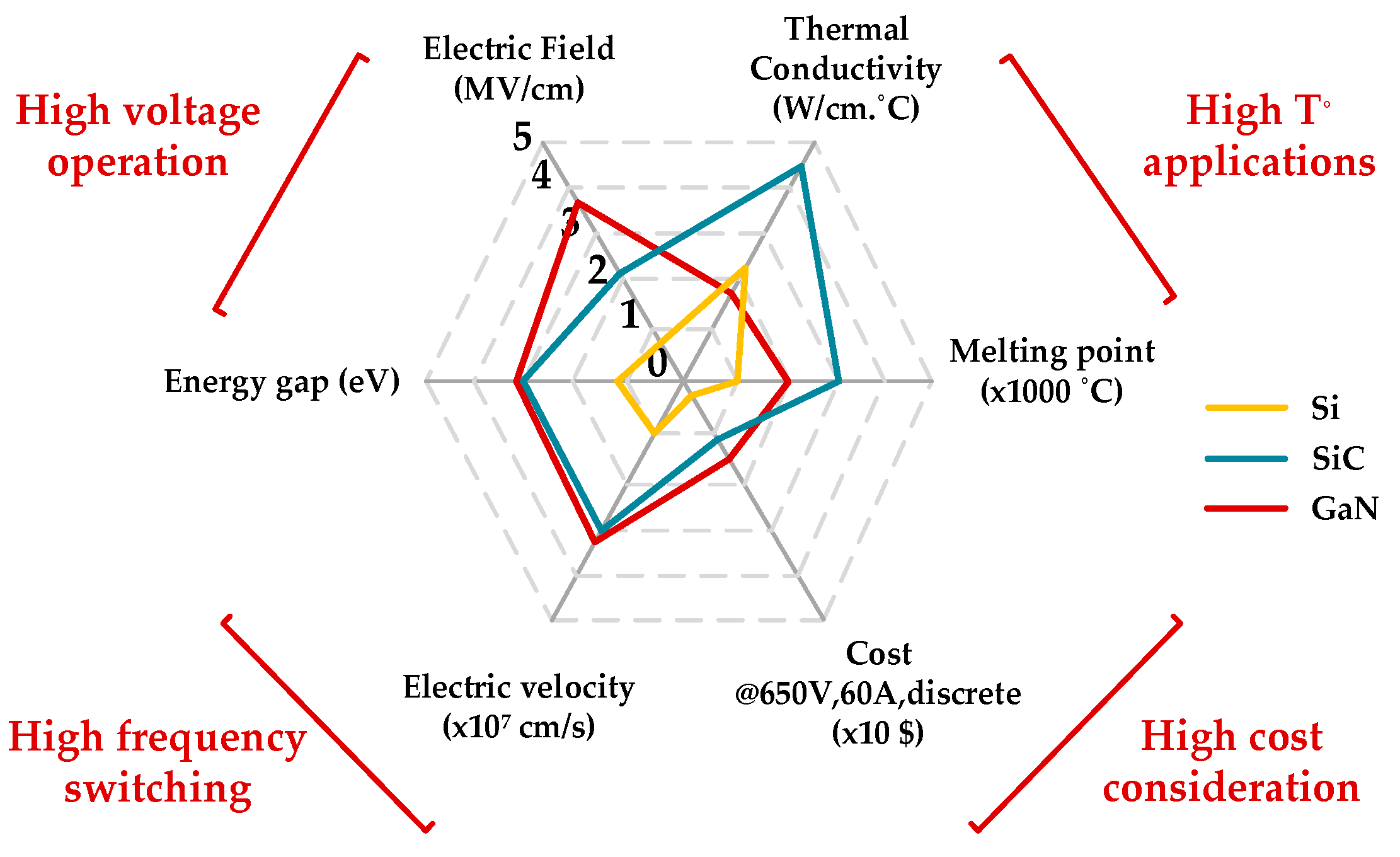
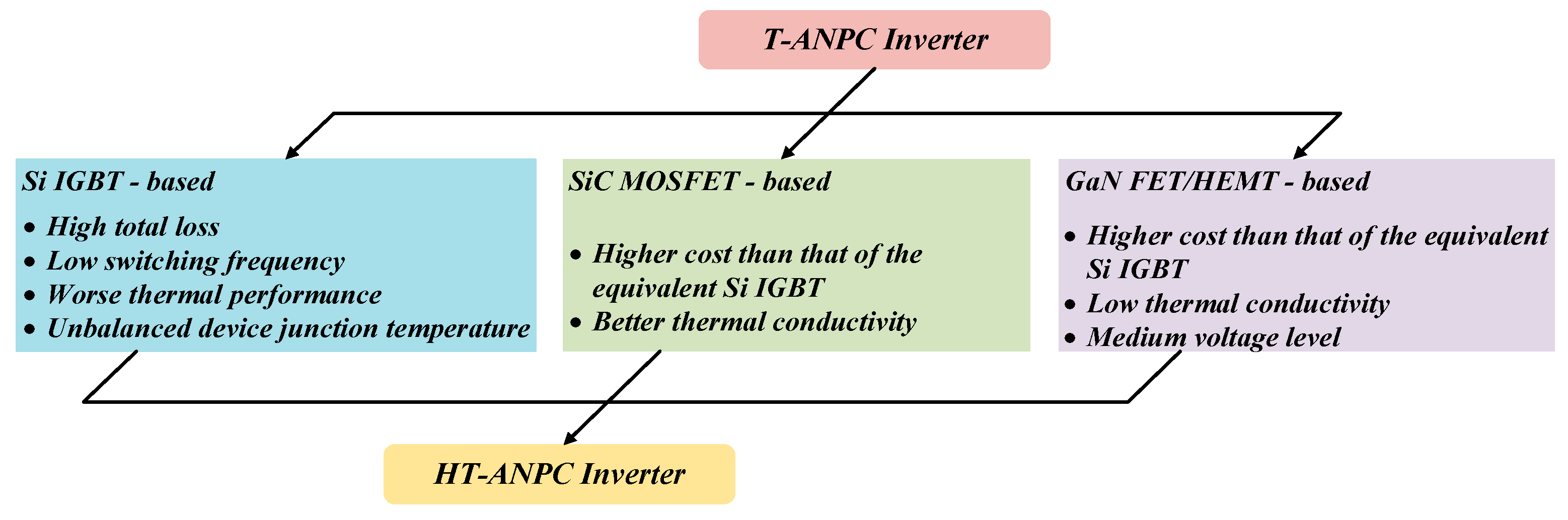

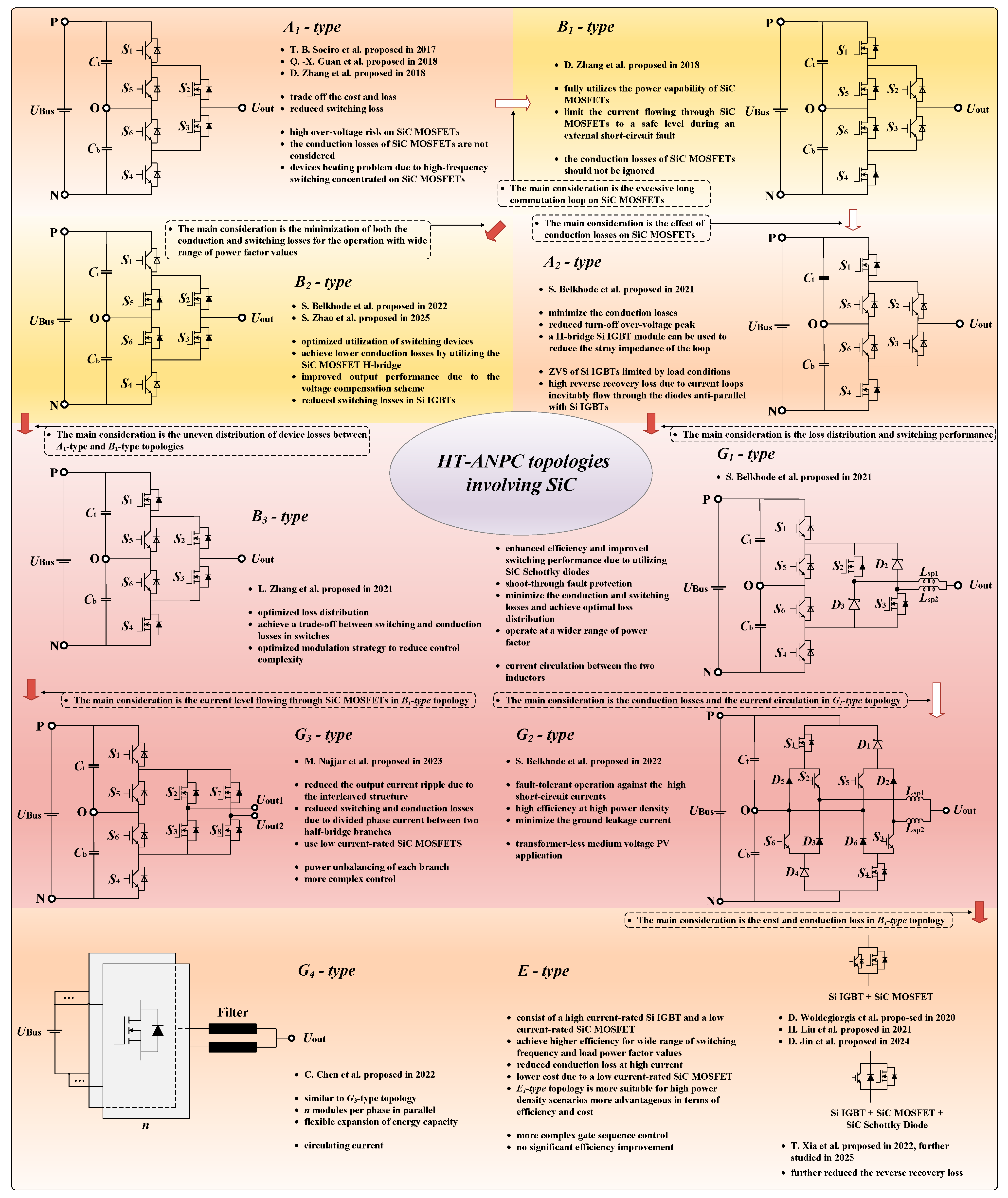

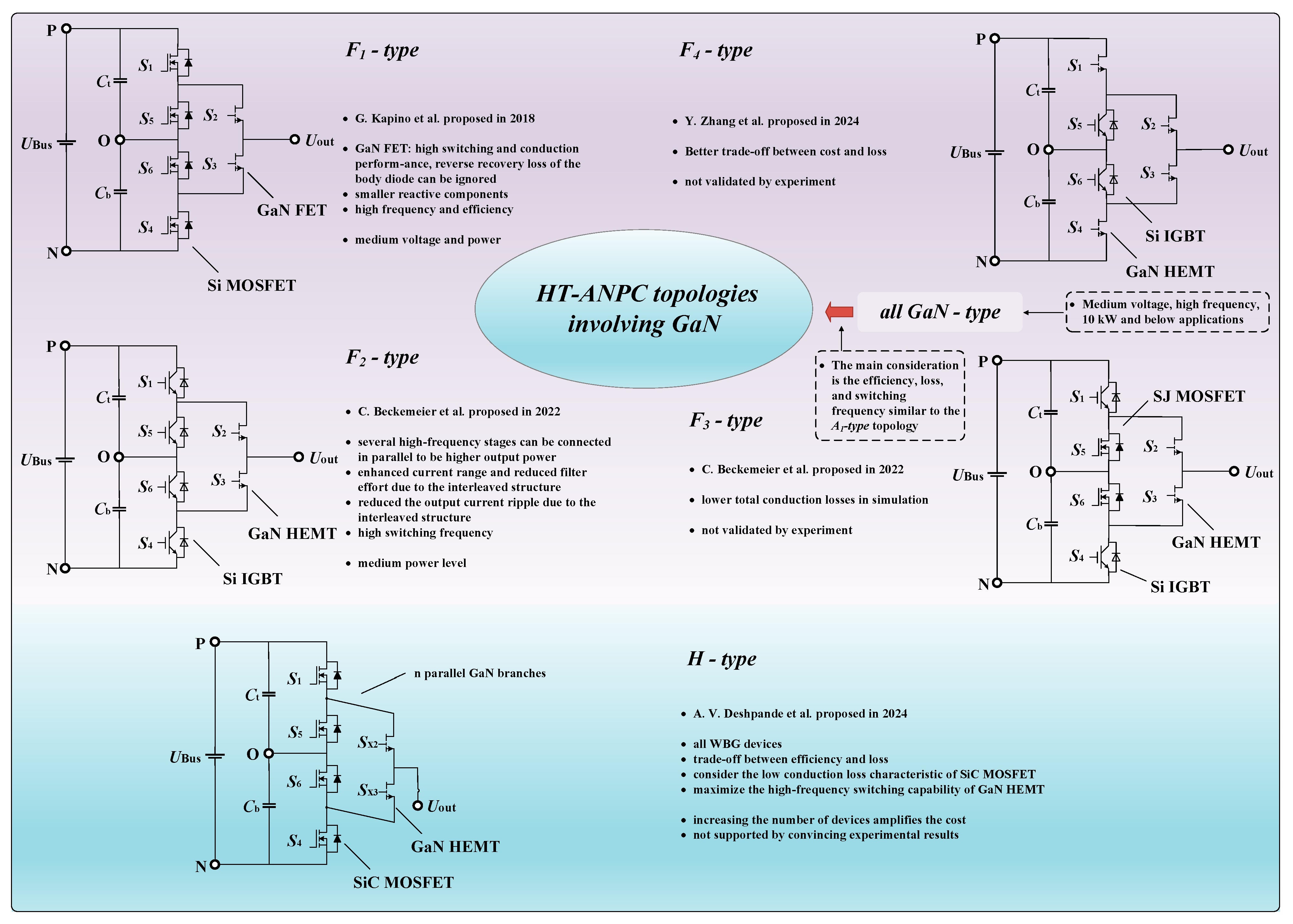
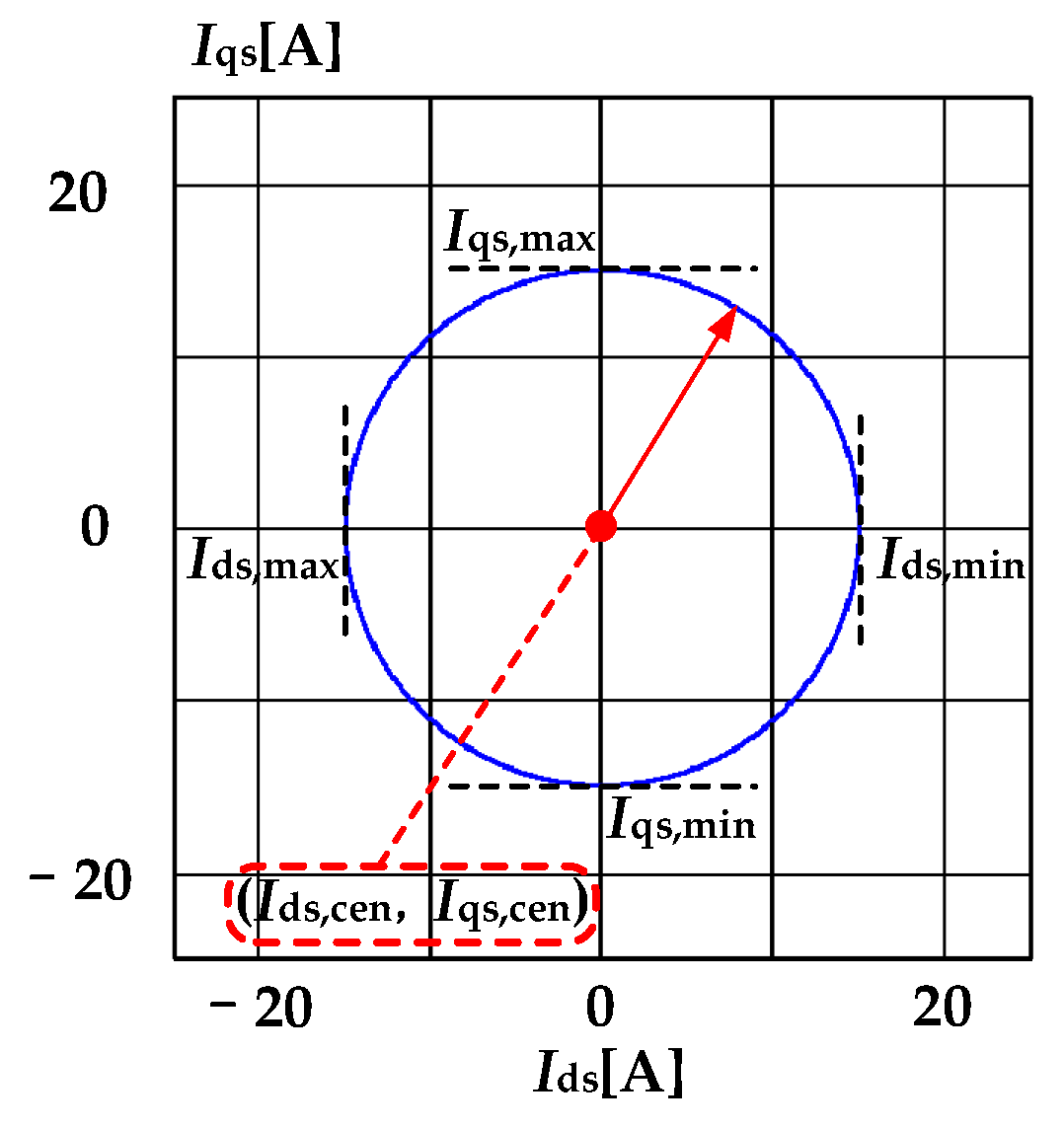
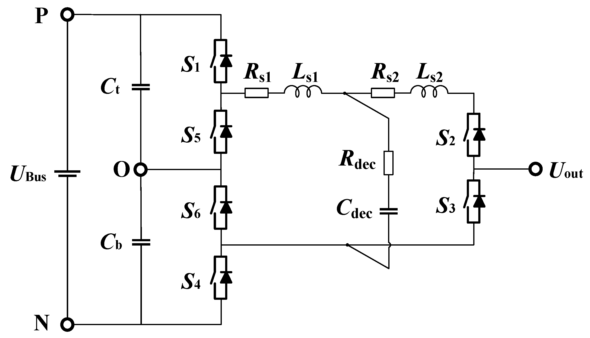
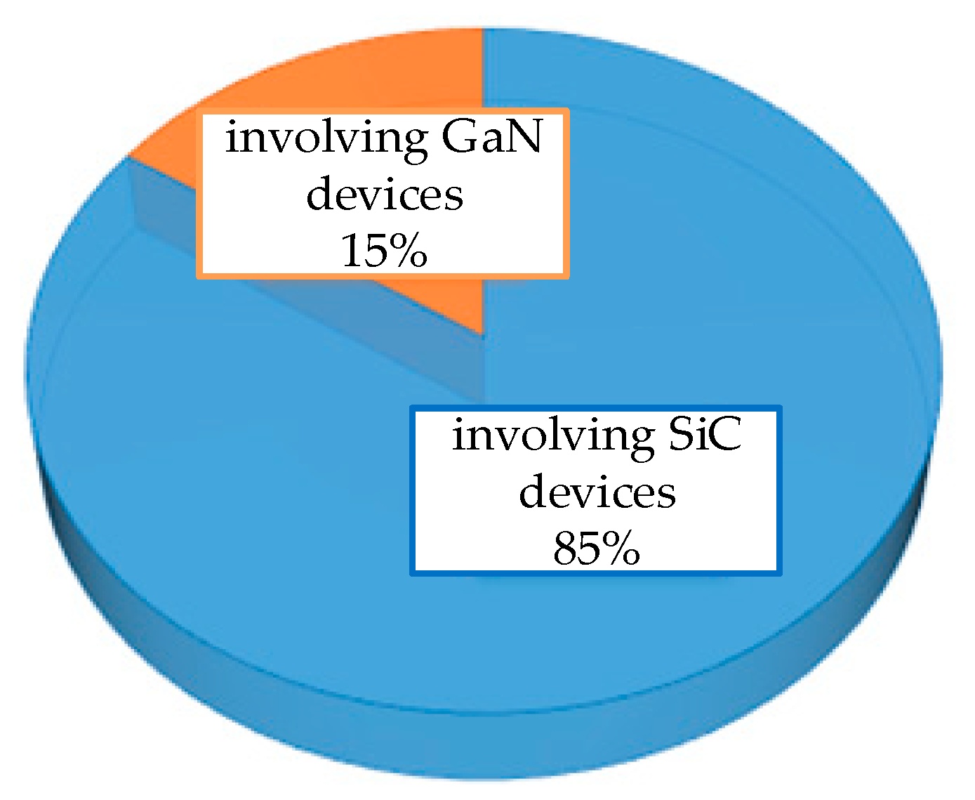
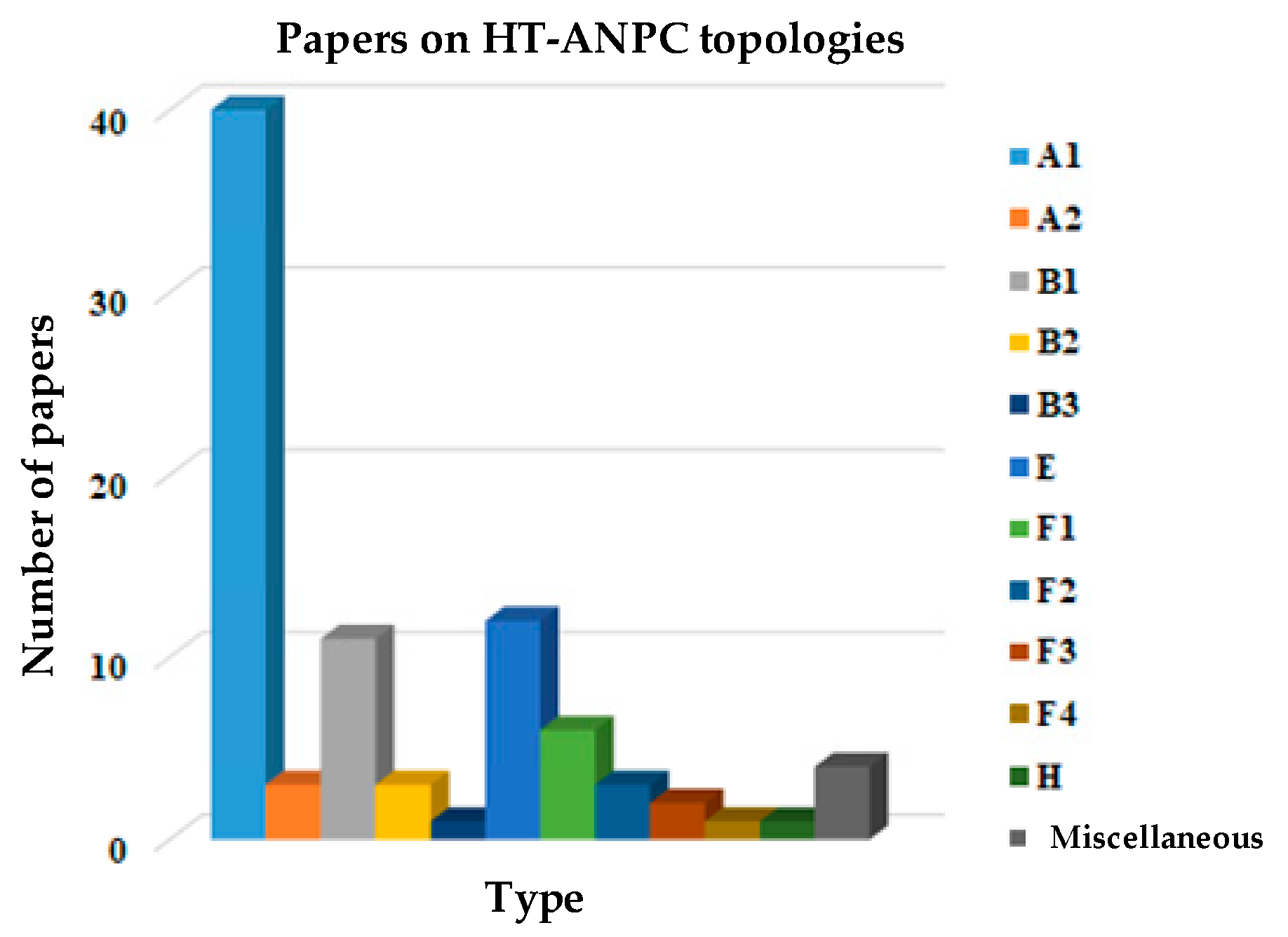
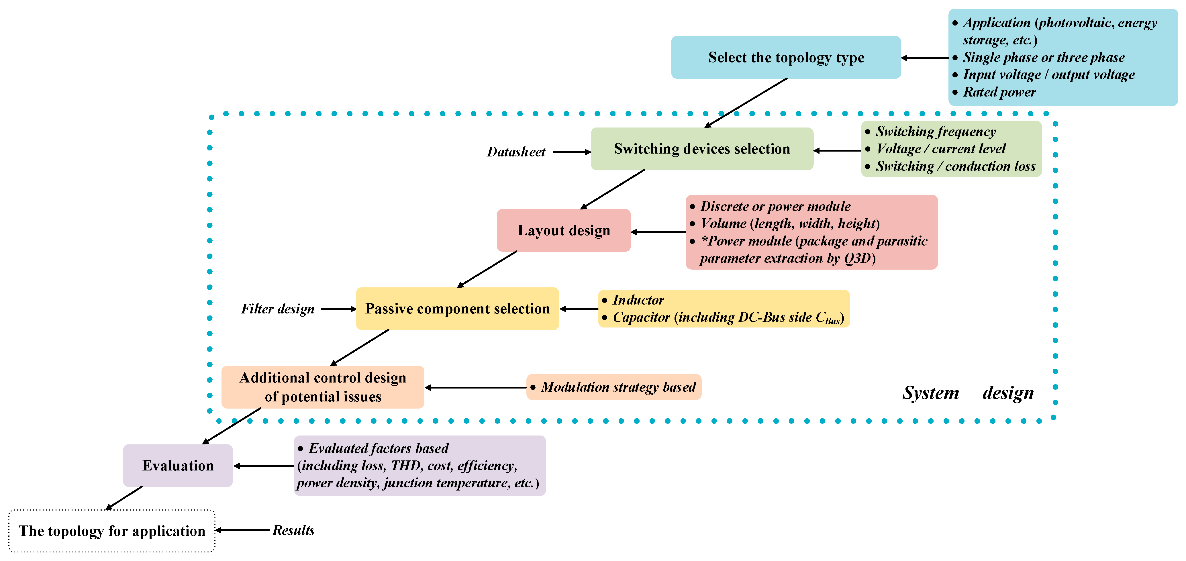
Disclaimer/Publisher’s Note: The statements, opinions and data contained in all publications are solely those of the individual author(s) and contributor(s) and not of MDPI and/or the editor(s). MDPI and/or the editor(s) disclaim responsibility for any injury to people or property resulting from any ideas, methods, instructions or products referred to in the content. |
© 2025 by the authors. Licensee MDPI, Basel, Switzerland. This article is an open access article distributed under the terms and conditions of the Creative Commons Attribution (CC BY) license (https://creativecommons.org/licenses/by/4.0/).