
Delta Modulation Technique and Harmonic Analysis for the Modified Quadruple-Diode Boost Regulator Without and With a Voltage Multiplier Unit (VMU)

 ,
,  ,
,
Abstract
1. Introduction
- Although the quadruple-diode boost regulator has more diodes and energy-storing components than the traditional step-up regulator, it nonetheless generates more power and, regrettably, higher voltage strain that is still within the permitted operating limits. However, the authors of this research also discussed this problem and provided the best solution;
- The quadruple-diode boost regulator outperforms the quadratic boost regulator (QBD), SEPIC regulators, and traditional step-up regulators in terms of voltage gain;
- The simulation and results in terms of regulator responsiveness, rising time, delaying response, effectiveness, and sensitivities to parameter variations validate the importance and preference of the DMCR as compared to other hysteresis (delta modulation) approaches covered in the literature [11,12];
- The performance of the delta modulation current regulator is evaluated by varying the delta modulation window limits, computing the harmonic content of the regulated current in terms of the corresponding harmonic ratio, and keeping the regulated current’s time derivative constant. The findings demonstrate that although the response speed stays constant, the delta modulation bandwidth has a significant effect on the quality of the regulated current. Therefore, considering the regulator restriction, a moderate delta modulation bandwidth was chosen;
- Based on the comparison study conducted for this work, QDBC is more useful than a typical step-up regulator, especially for solar panels, electric cars, and high-power renewable energy systems;
- When compared to step-up regulators such as SEPIC, boost, and buck-boost, the proposed configuration greatly reduces many harmonics emitted at the input and output with high effectiveness;
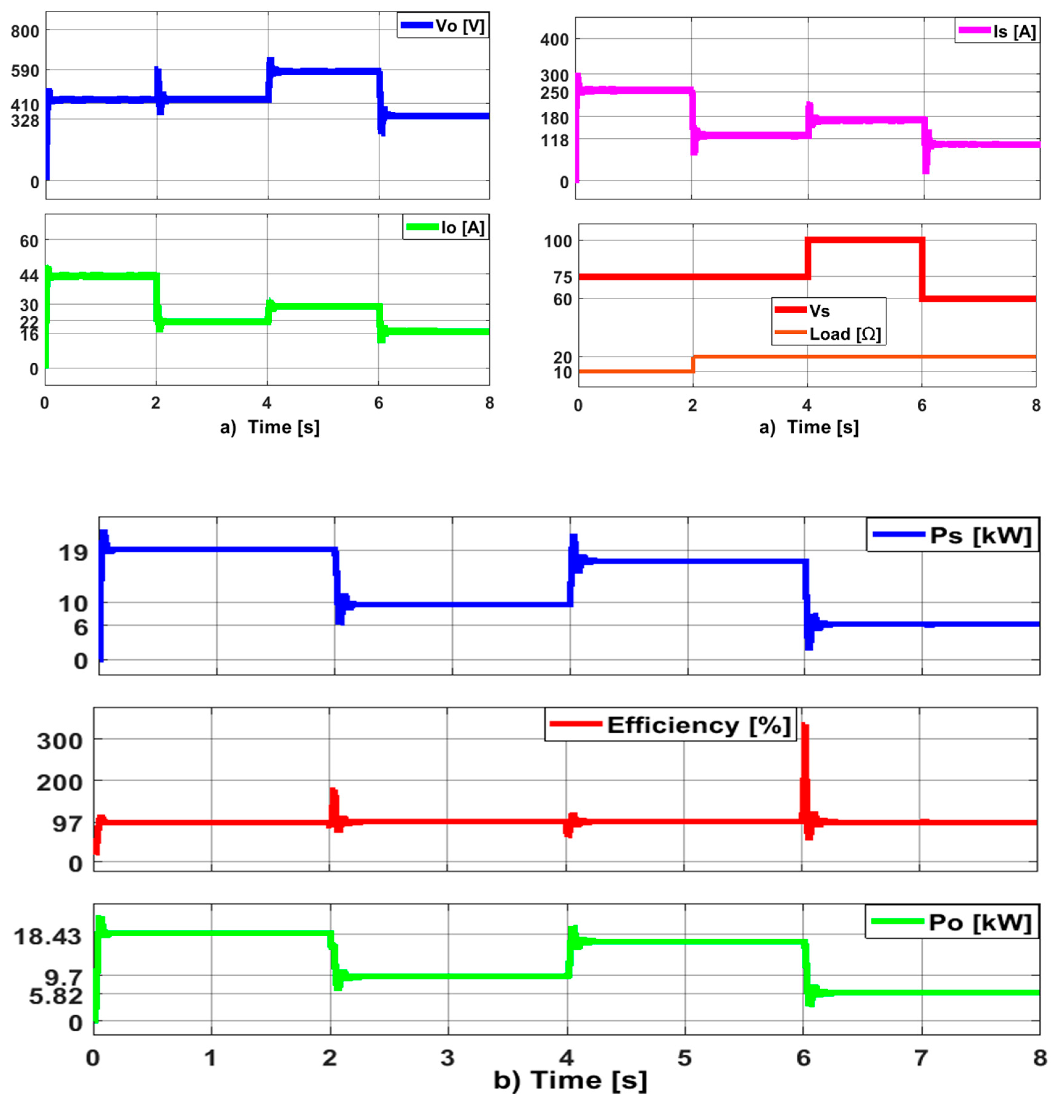
- The suggested quadratic boost regulator’s effectiveness has been assessed under a range of operational conditions, including supply voltages and loading scenarios. It has also been investigated during the laboratory simulation and analysis of the suggested converter at various switching frequencies. The simulated and analytical findings show that the efficiency level of the suggested QDBC regulator is 97%;
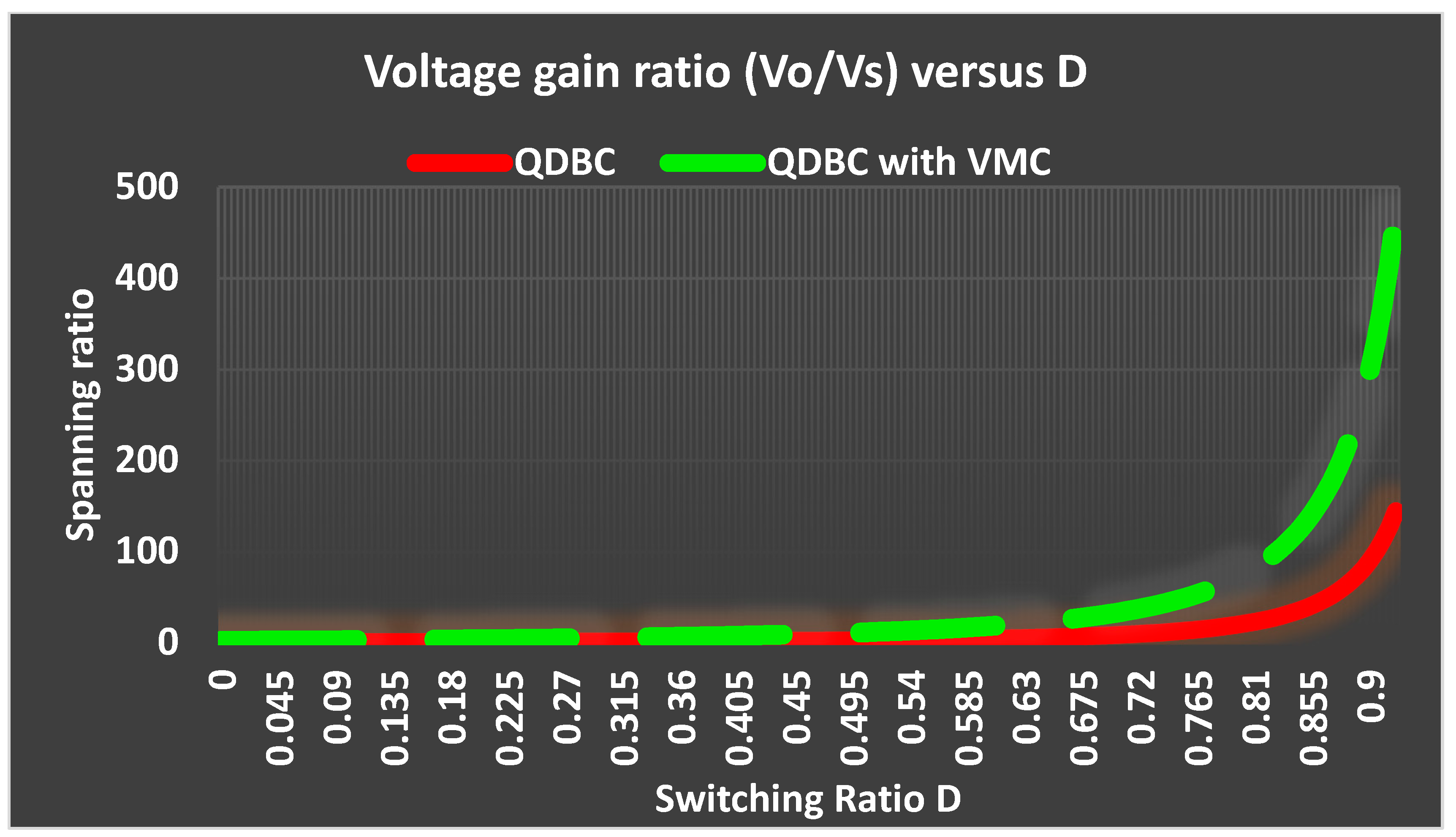
- The voltage gain of the suggested regulator is . This is larger than many other DC–DC regulators, including those suggested in [9,10,11,12,13,14]. Furthermore, adding the voltage multiplication circuit at the output of the proposed regulator (VMU) creates a new opportunity to have a regulator with a much greater voltage gain than others. The voltage gain of the suggested regulator with the VMU filter becomes ;
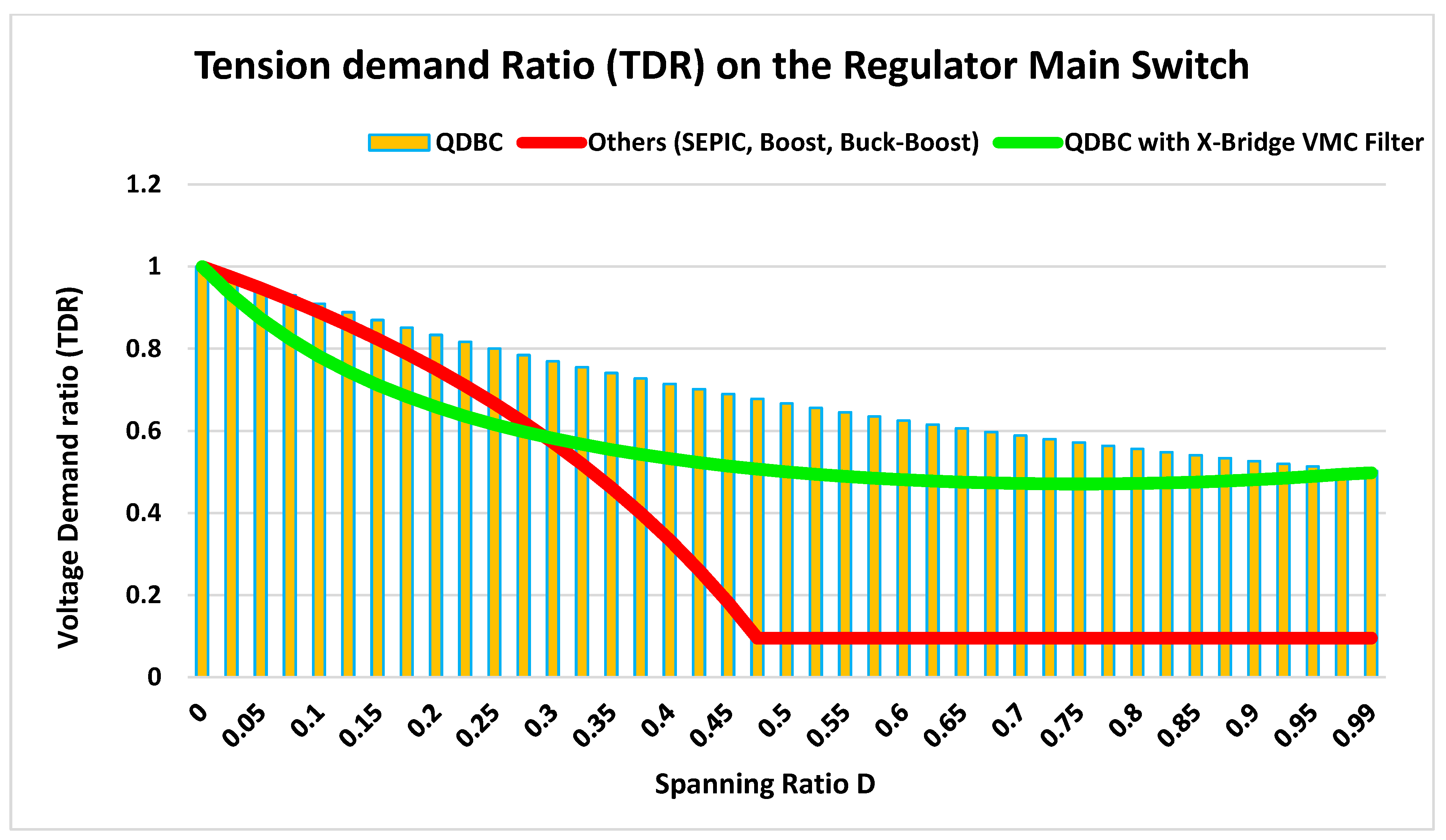
- The VMU filters at the regulator’s output can also be used to lessen the increased voltage tension (strain) on both passive and active switches.
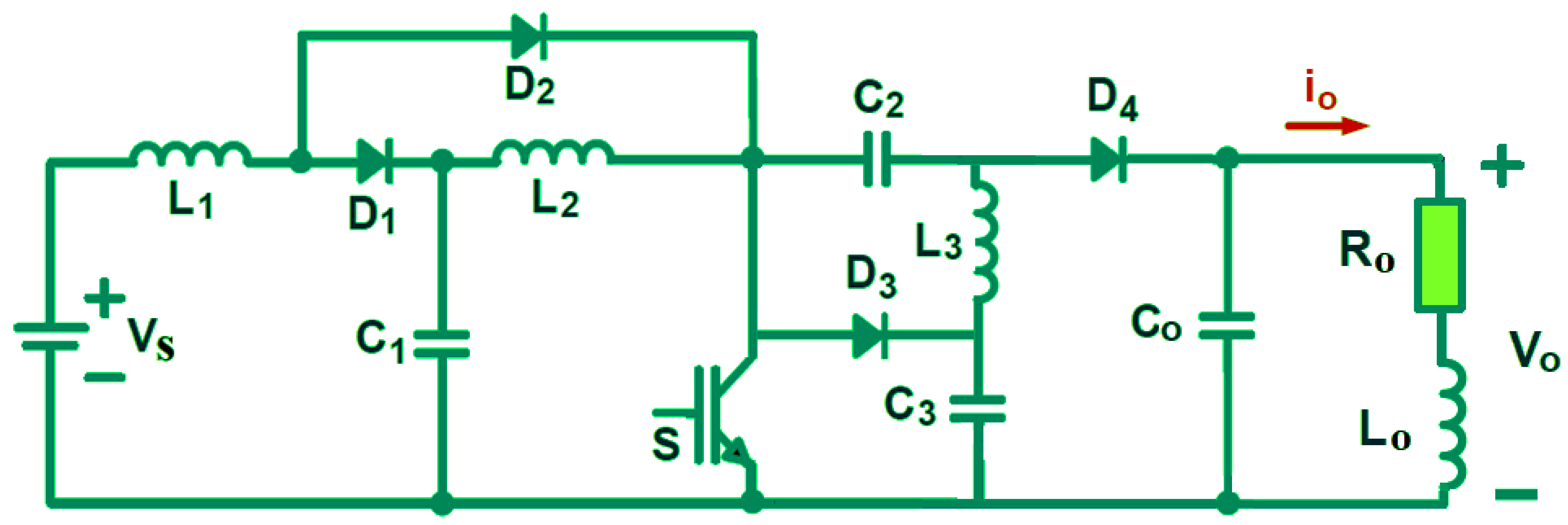
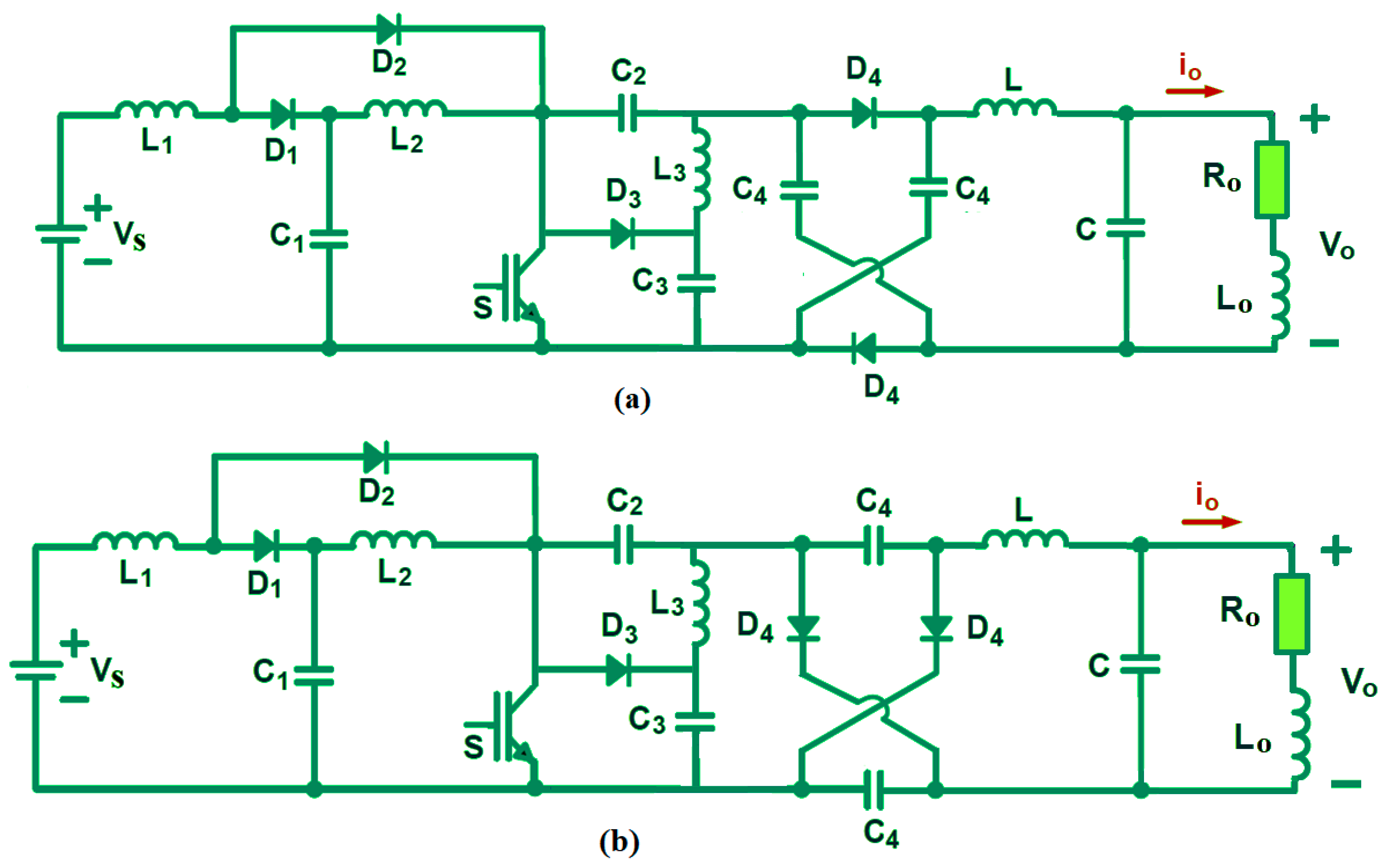
2. An Elementary Analysis of Quadruple-Diode Boost Regulator (QDBC)
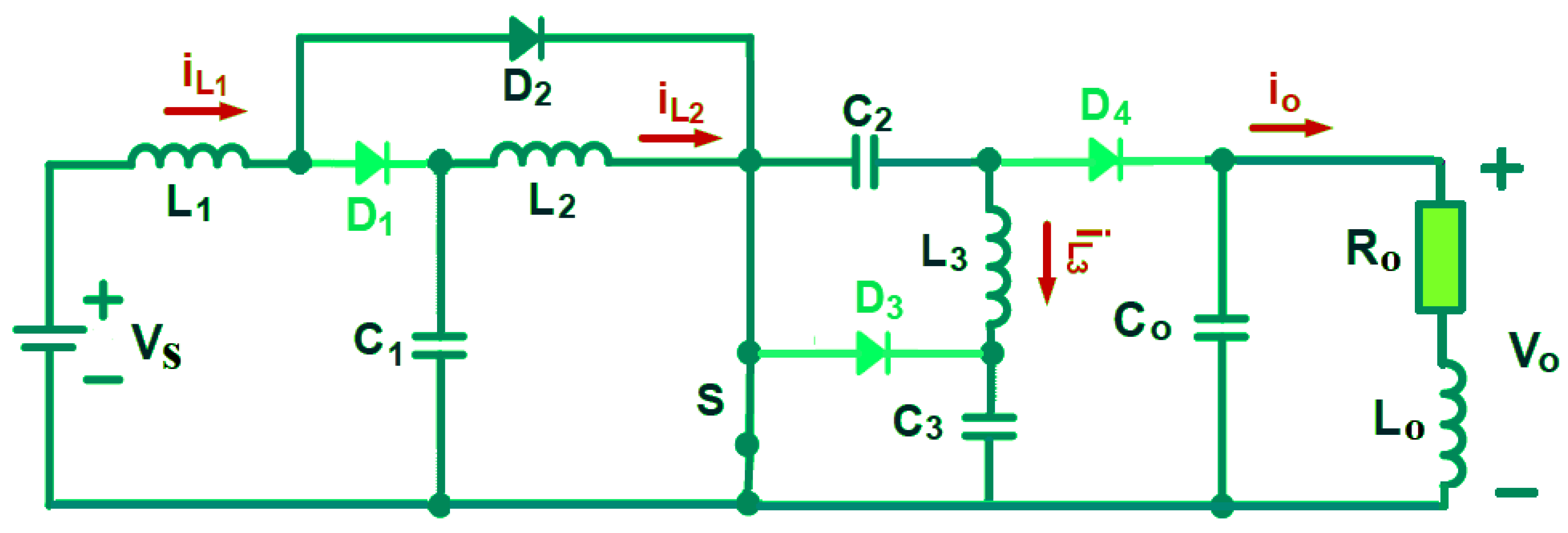
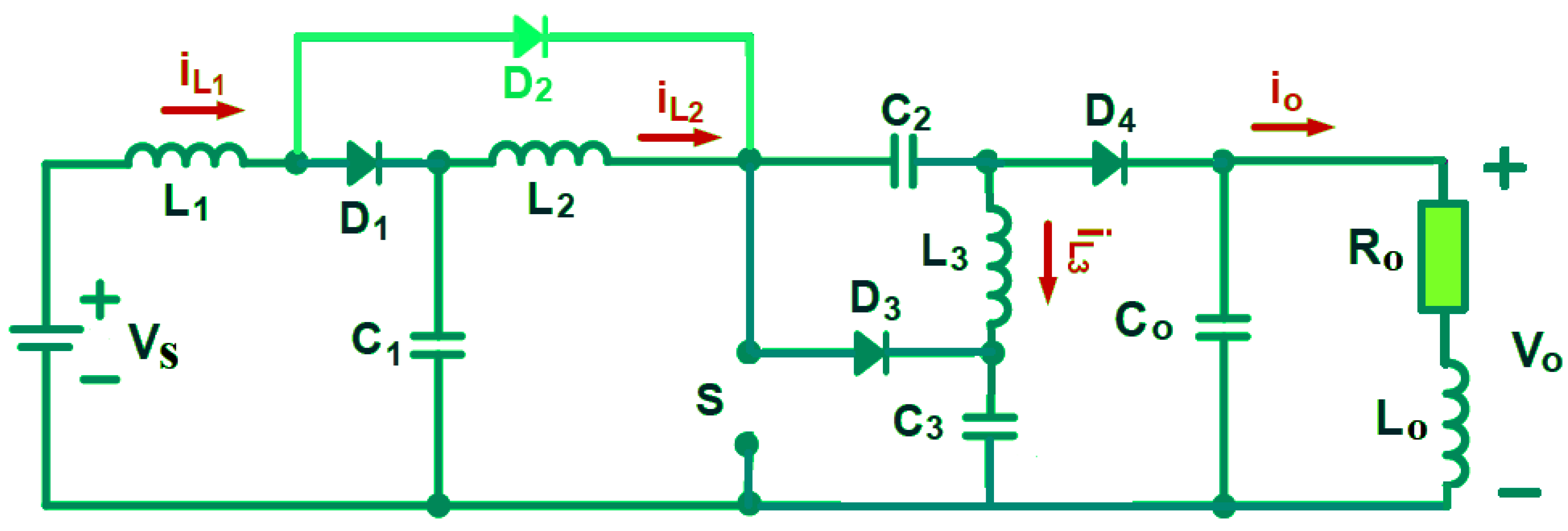
2.1. Operating Principle of QDBC Without an VMU Filter
2.2. Operating Principle of QDBC with a Voltage Multiplier Unit (VMU)
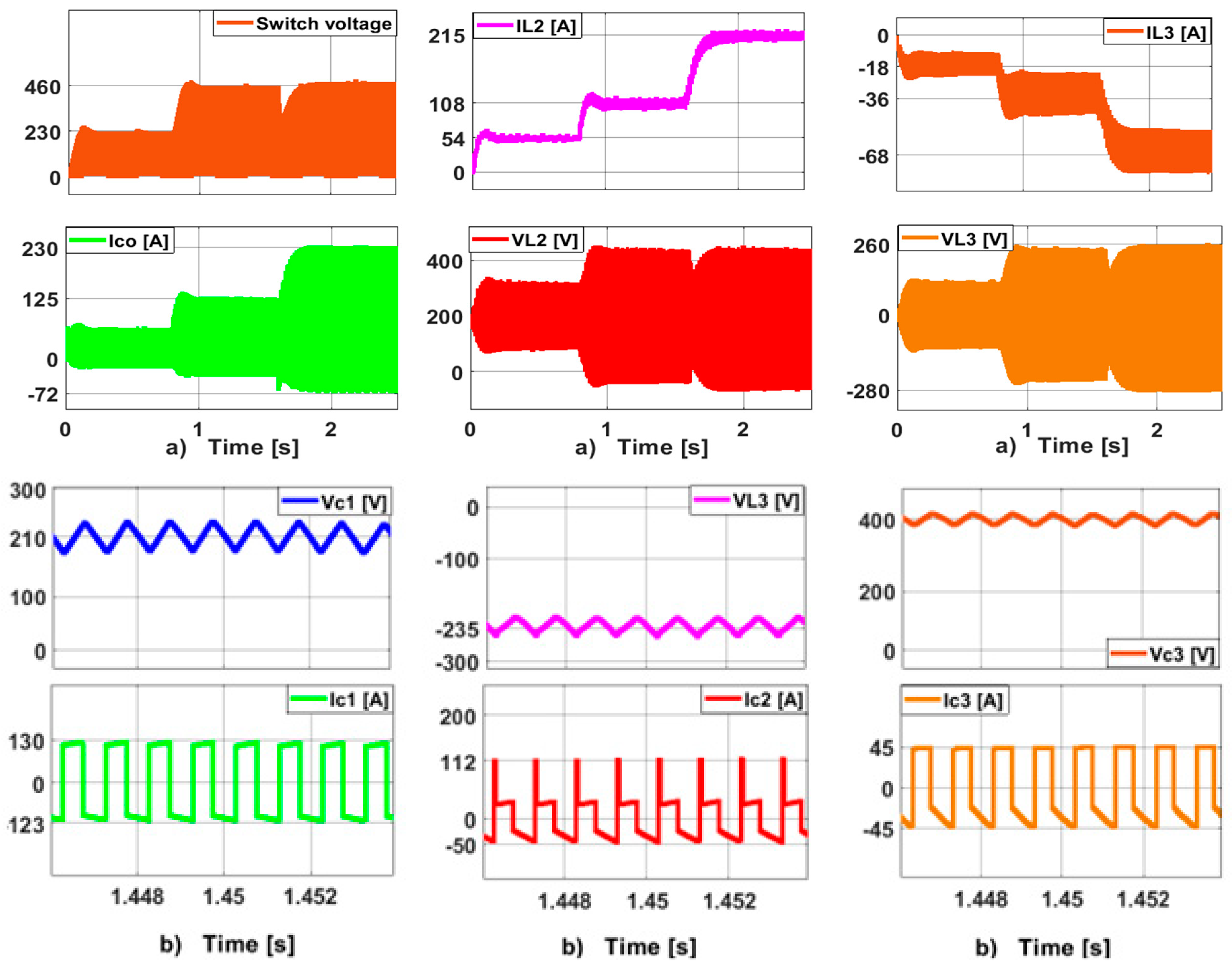
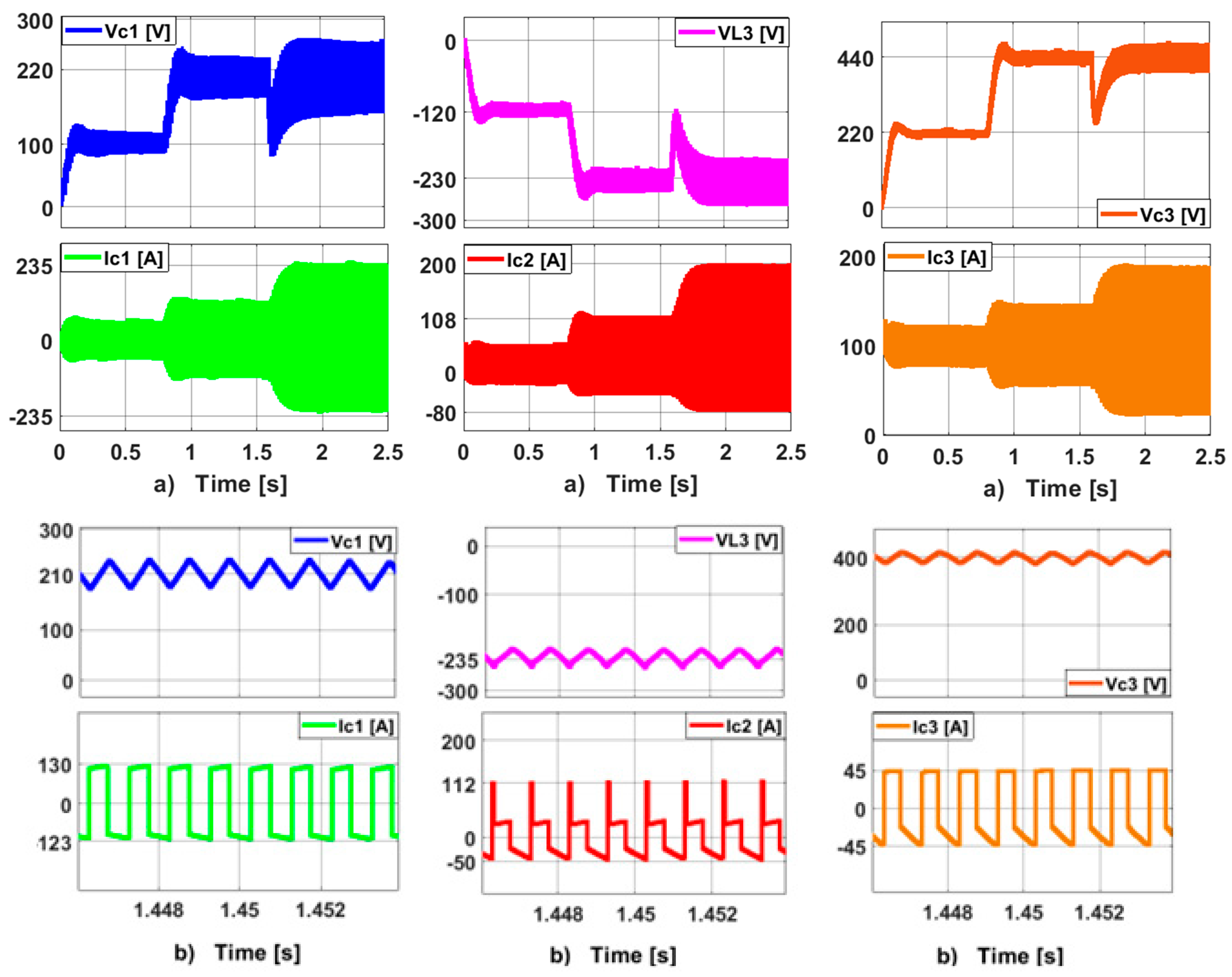
2.3. Normalized Inductive Choke Current and Capacitive Filter Voltage Fluctuation
2.4. Tension Demand Ratio (TDR) on the QDBC Essential Switch
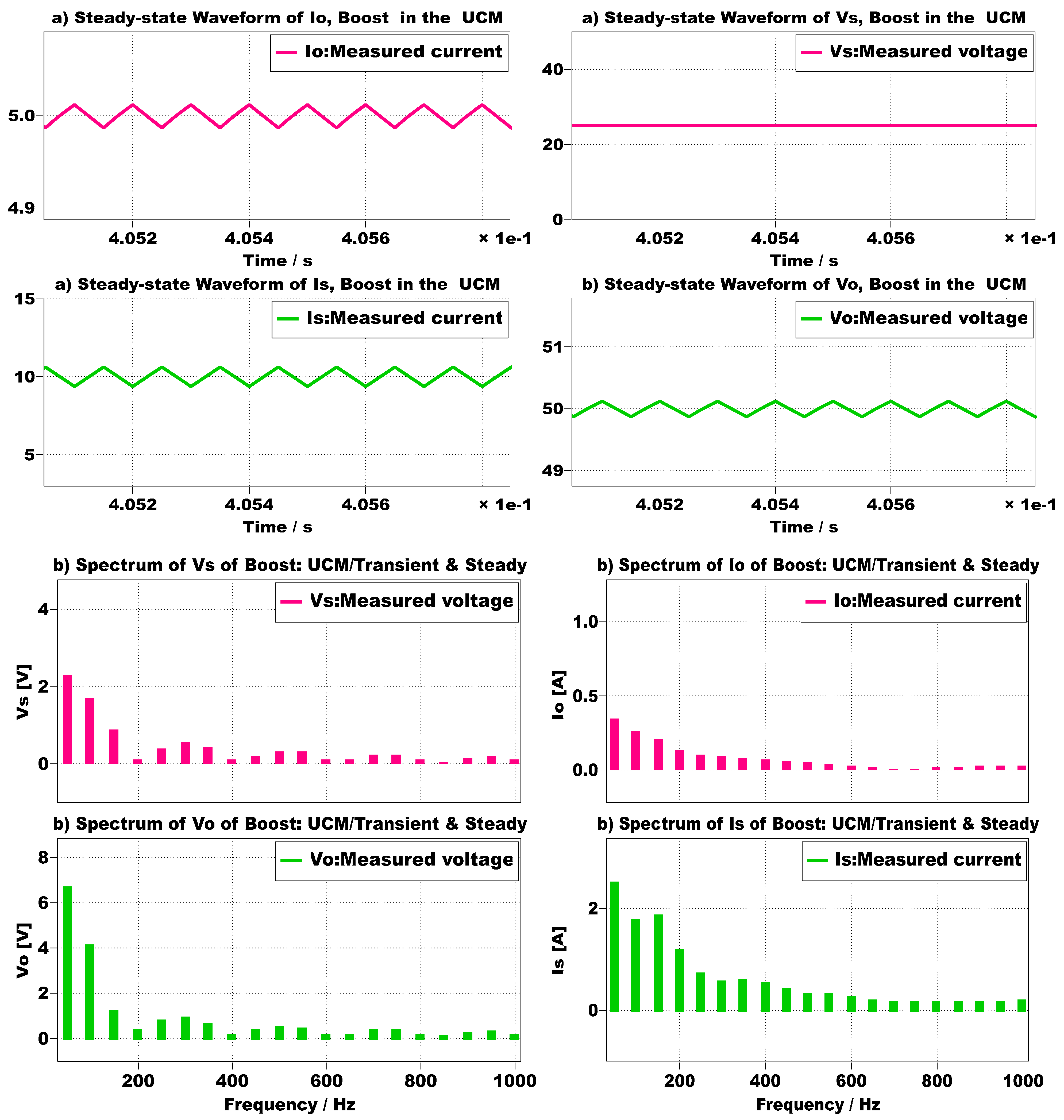
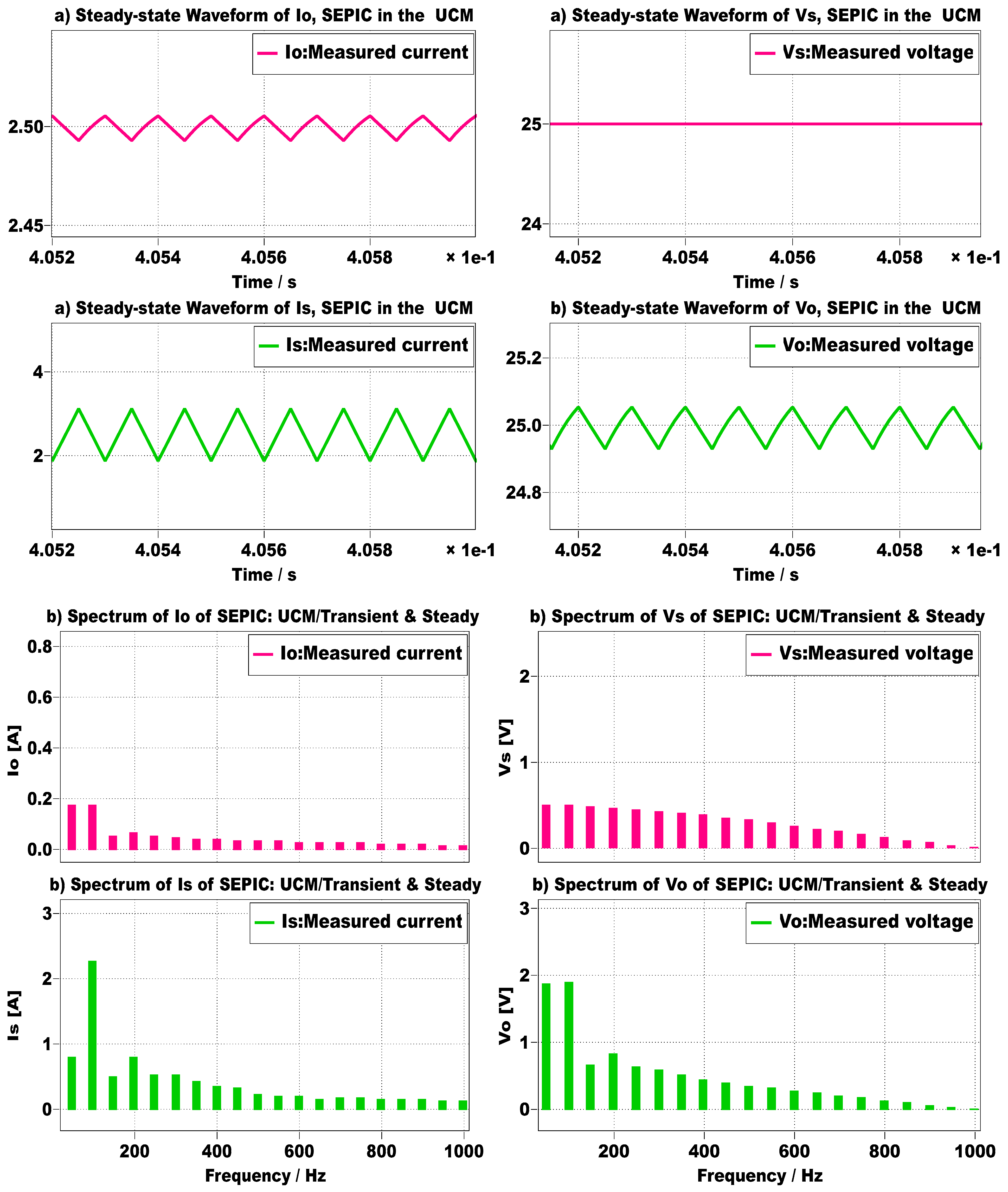
3. Harmonic Spectrum of QDBC Regulator
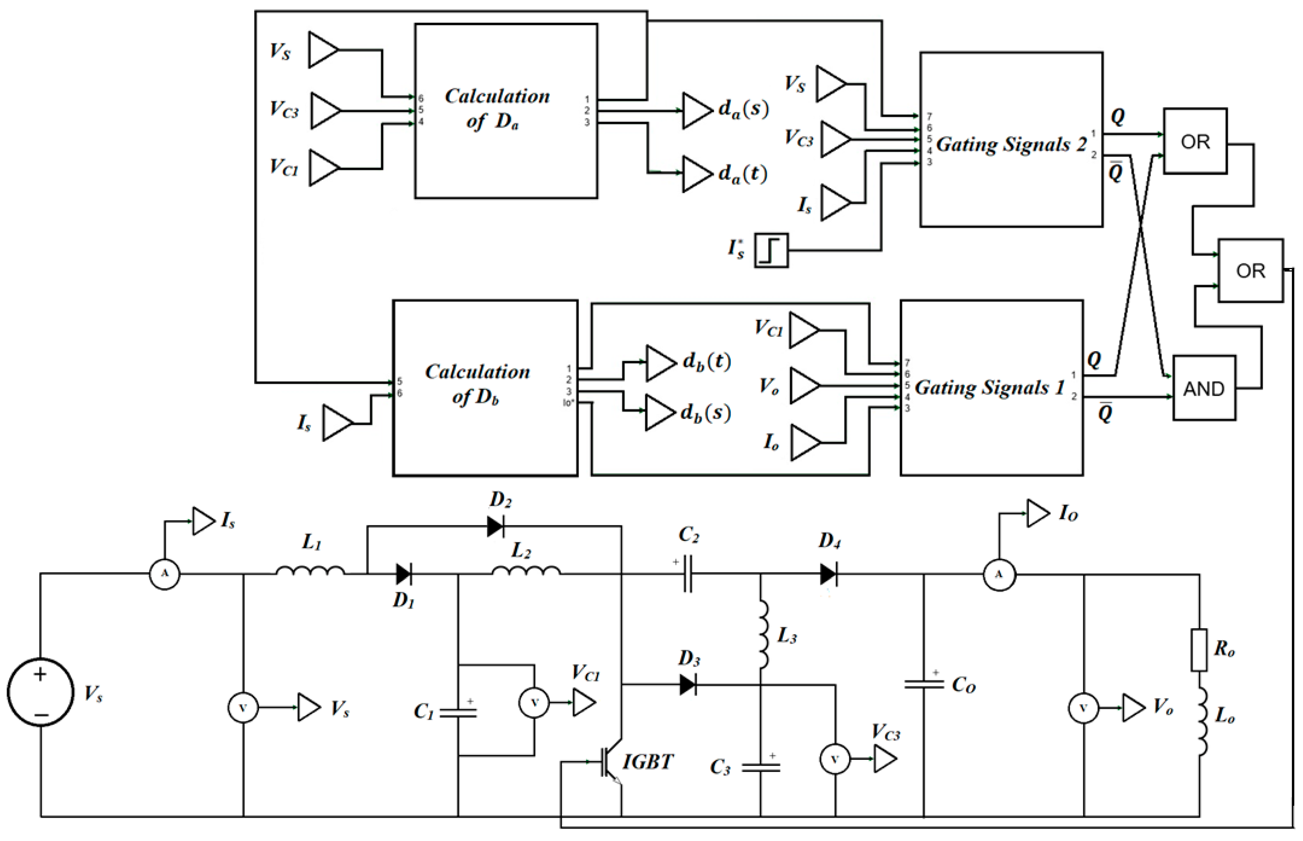
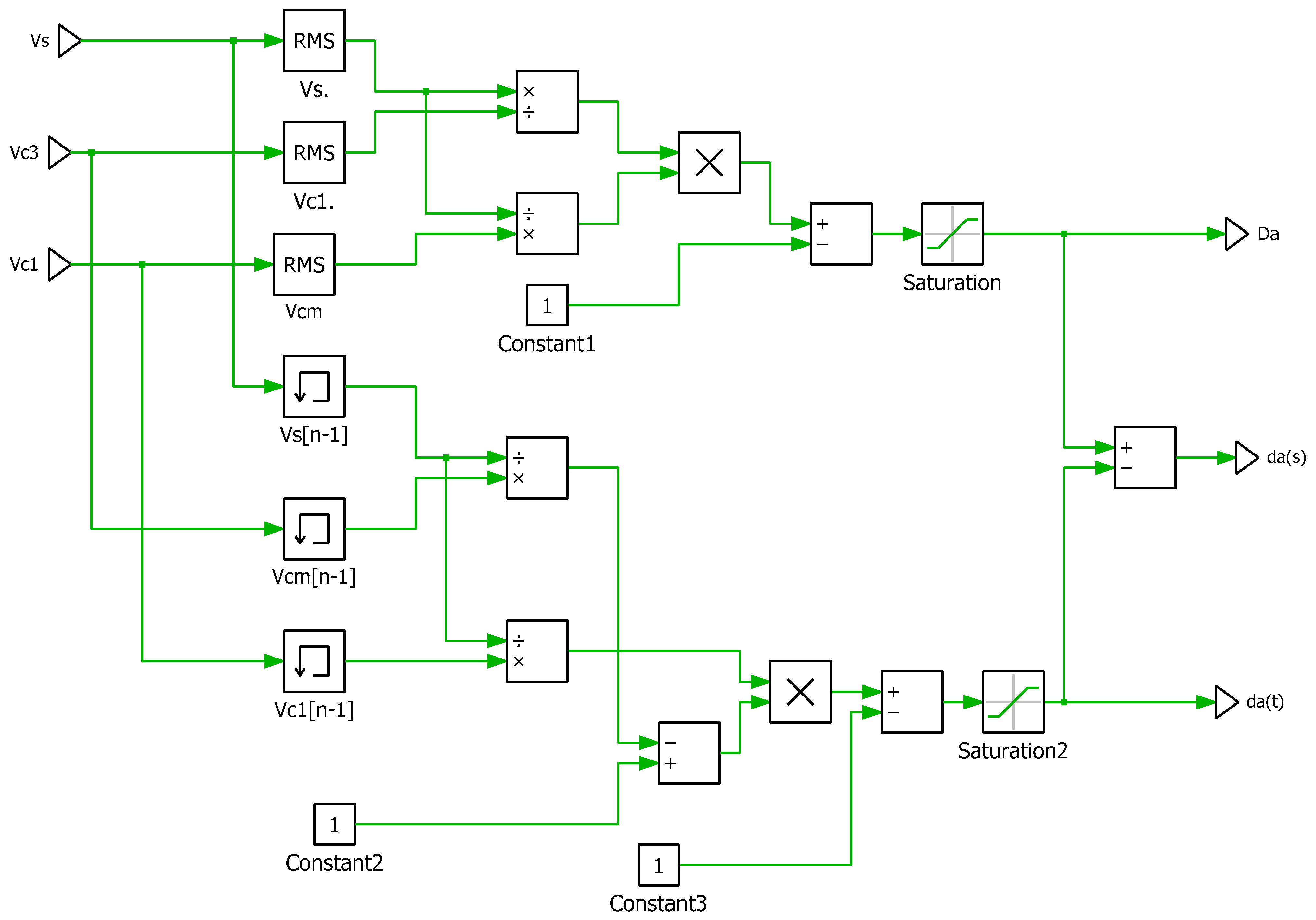
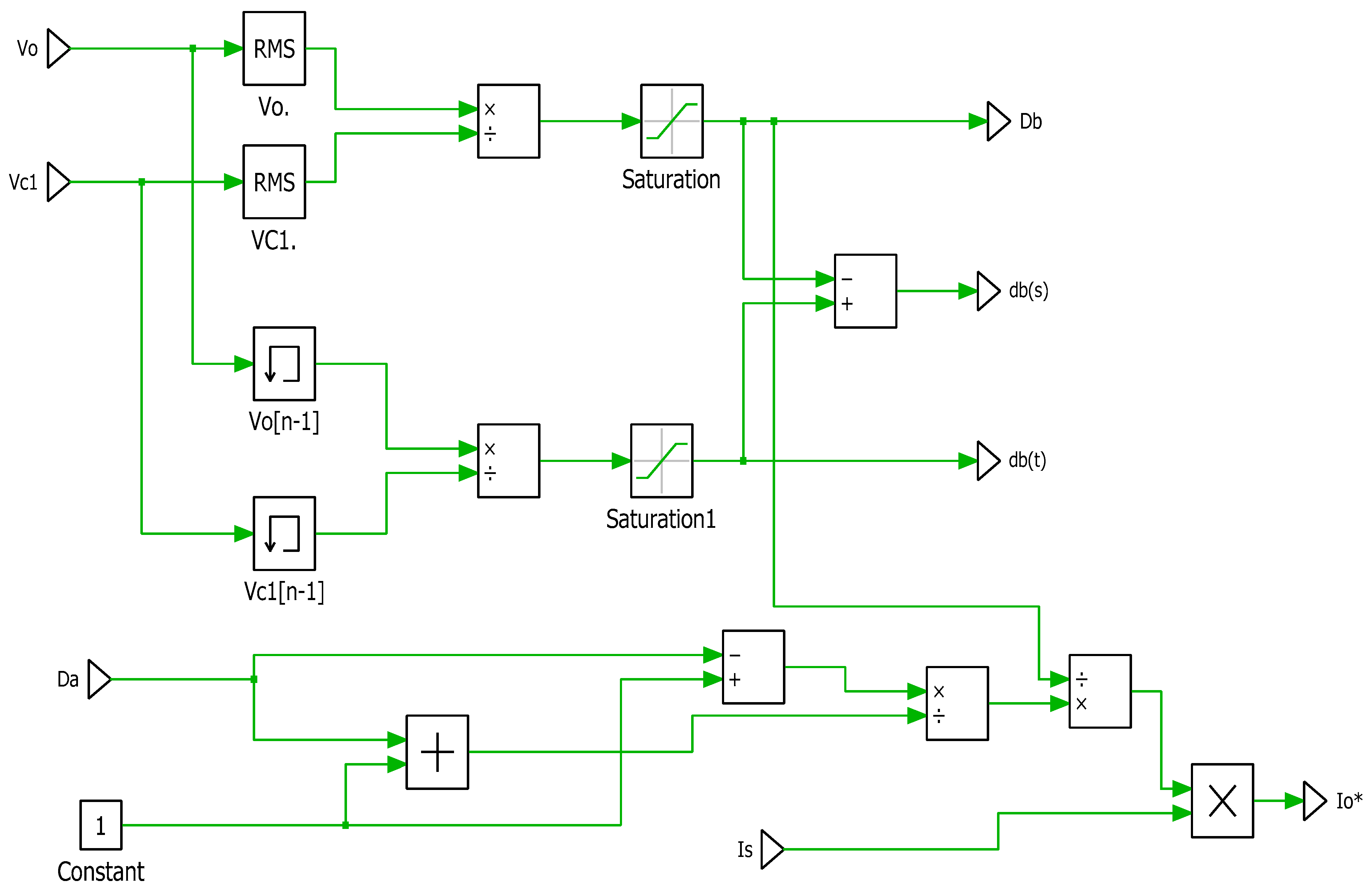
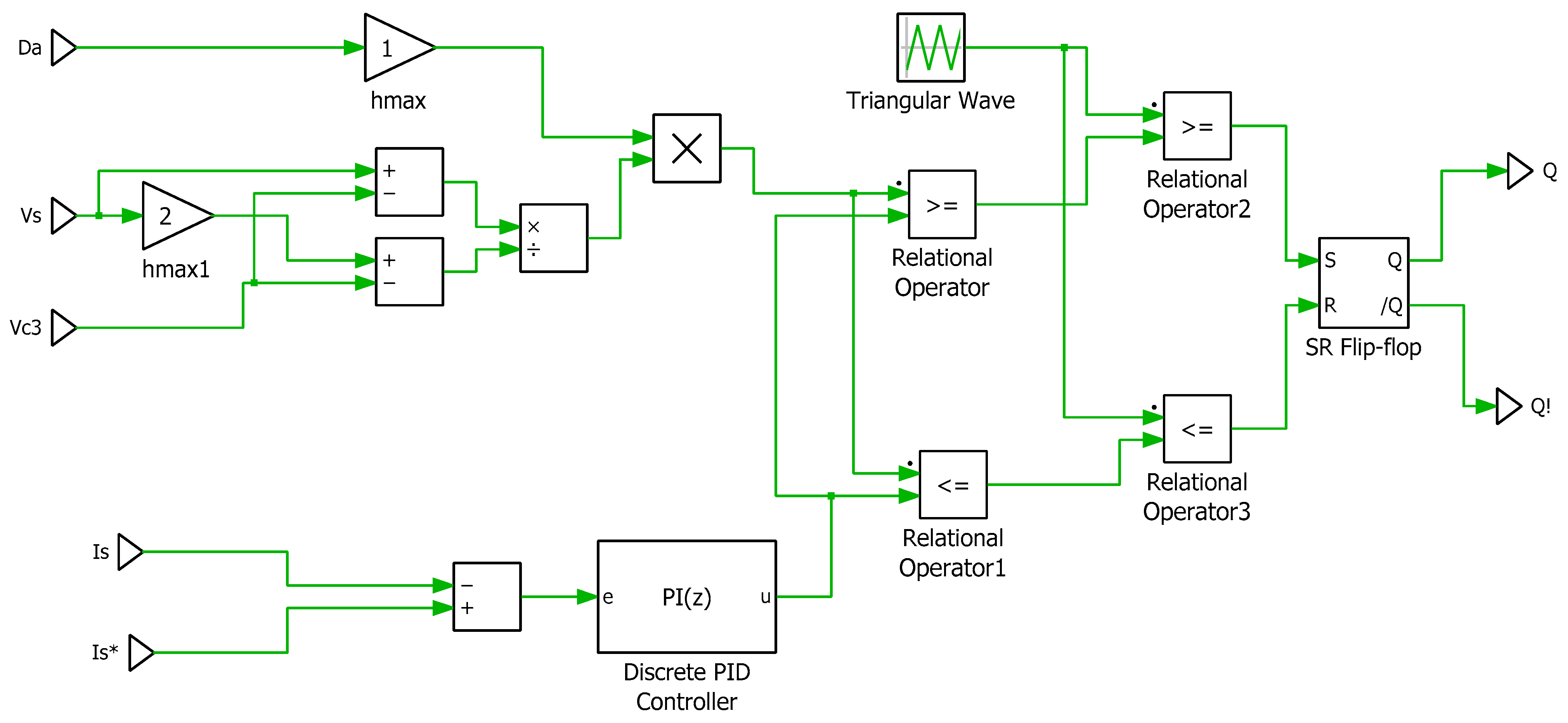
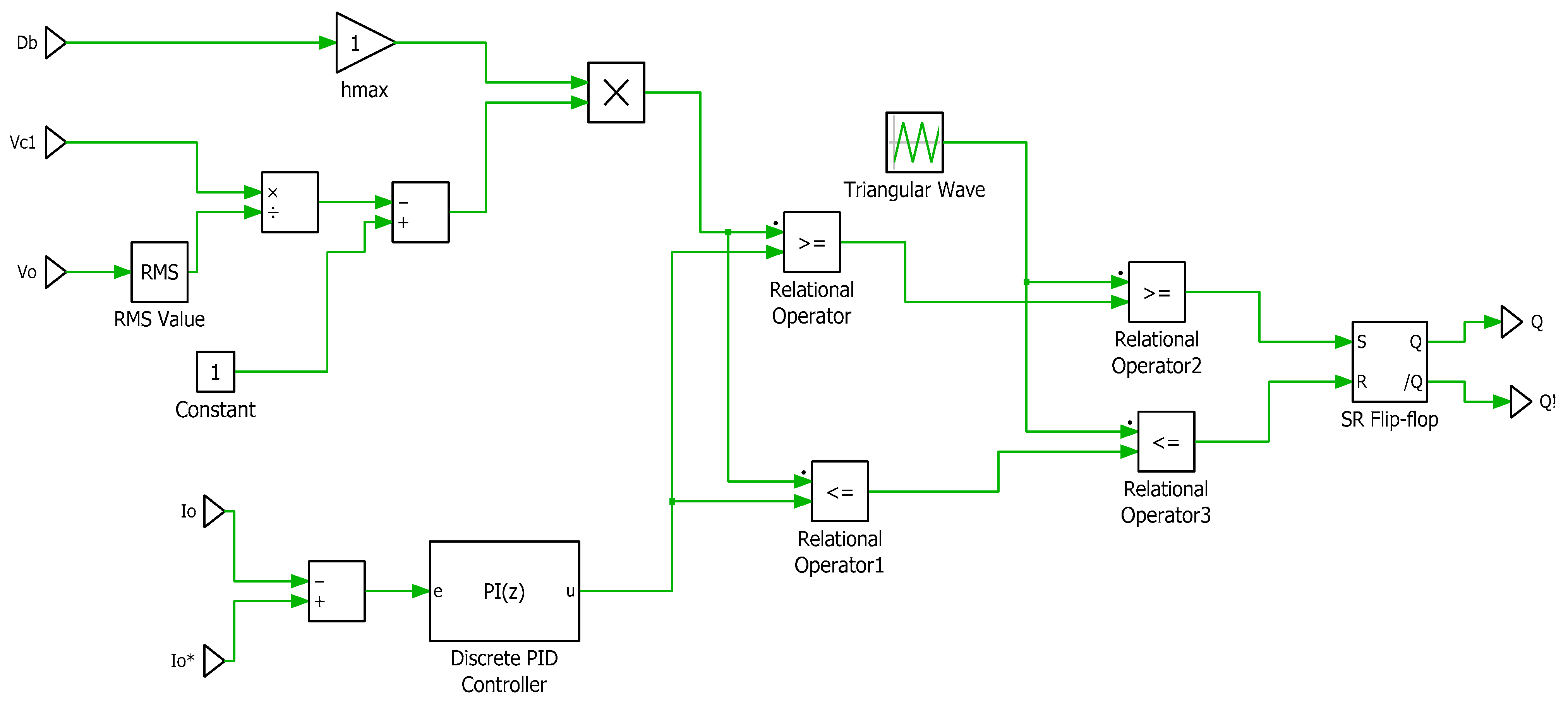
4. Regulation Method of QDBC Regulator
Delta Modulation Current Regulator (DMCR)
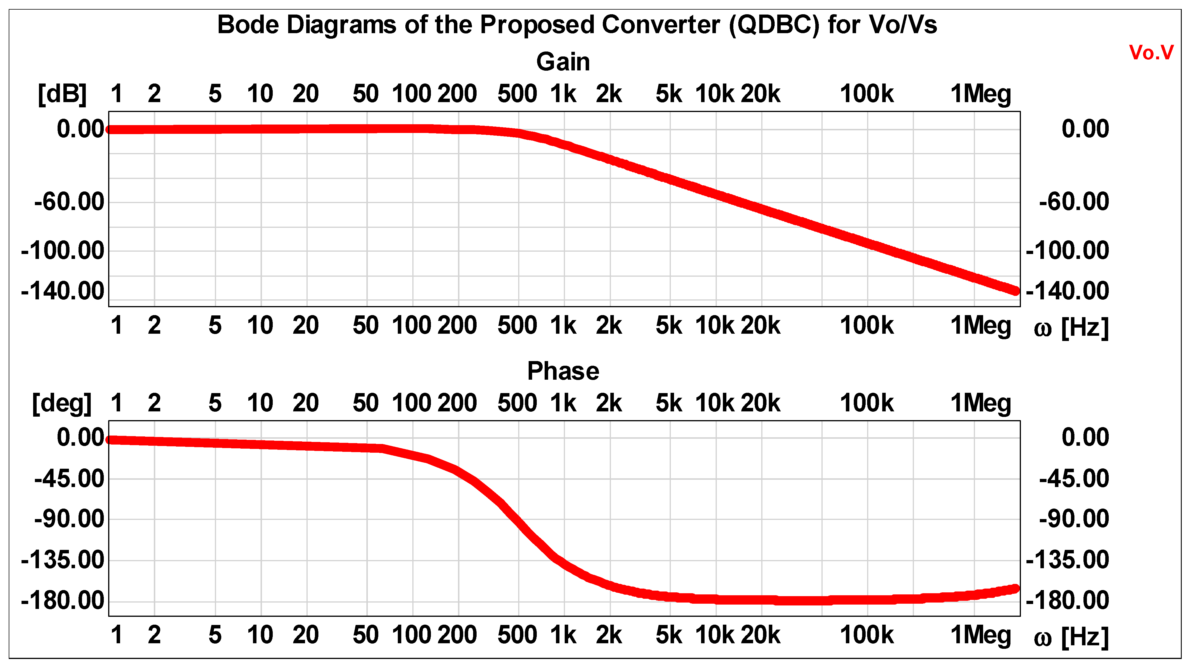
5. The Frequency Response of the Recommended QDBC Regulator
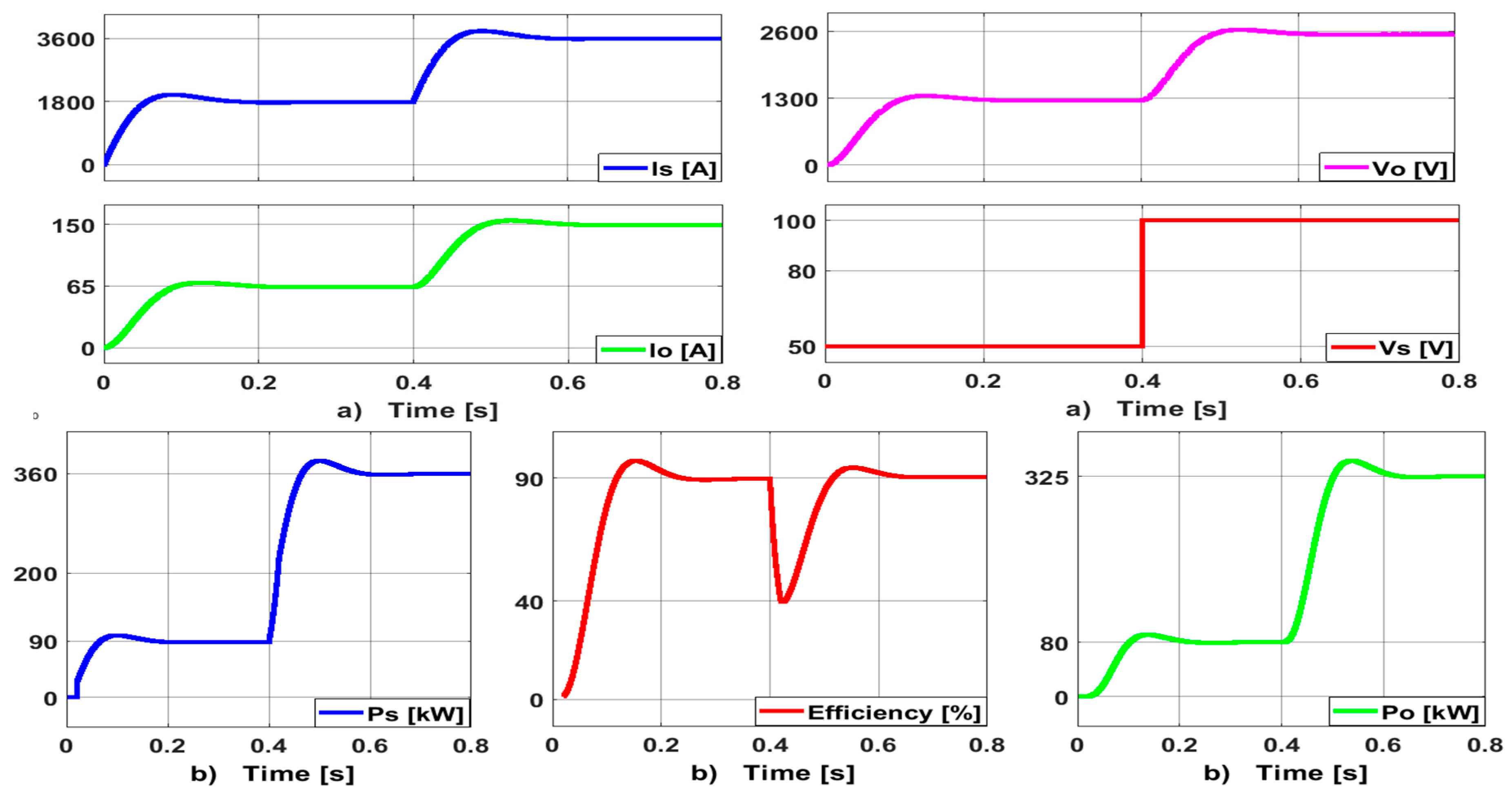
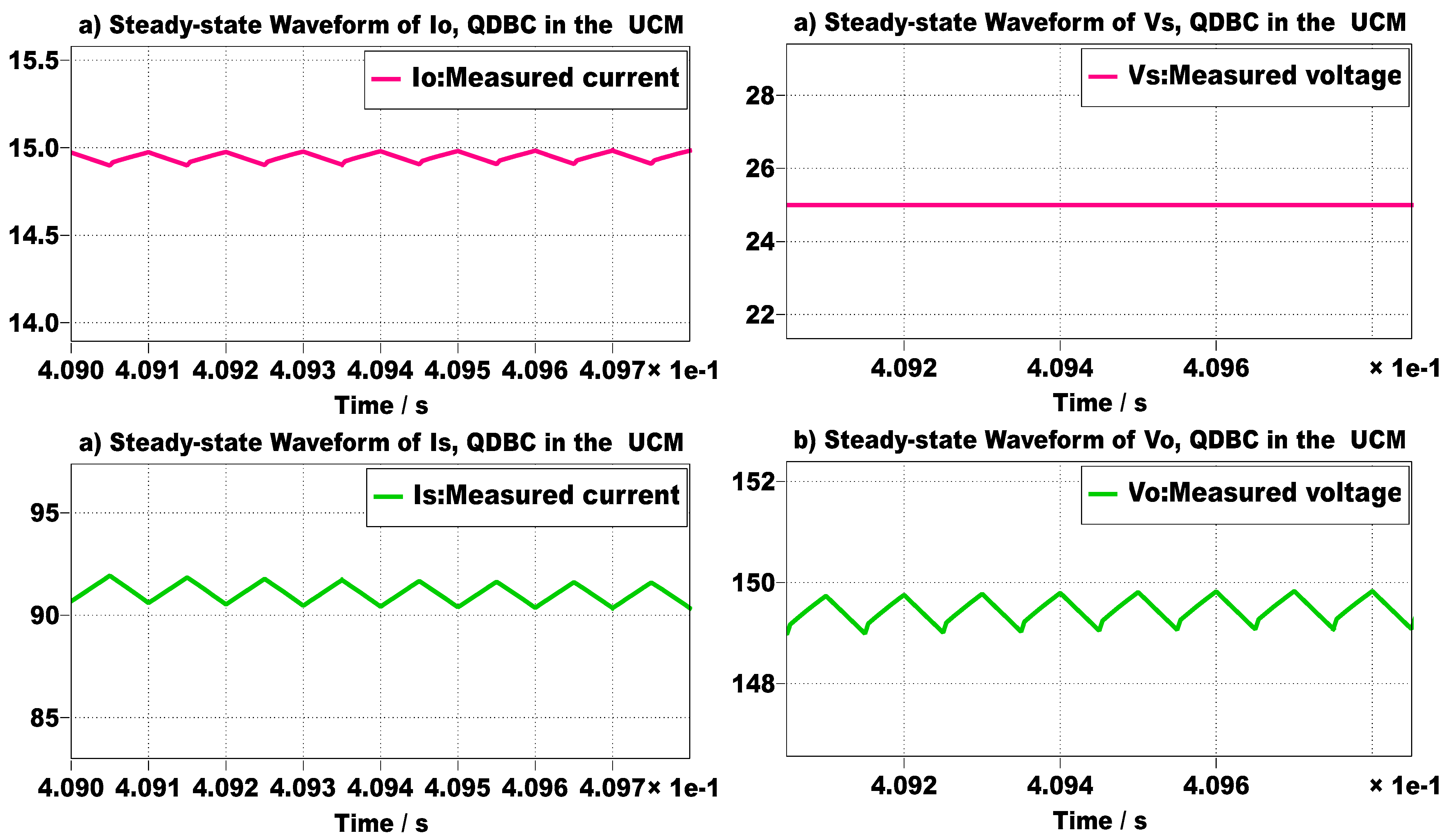
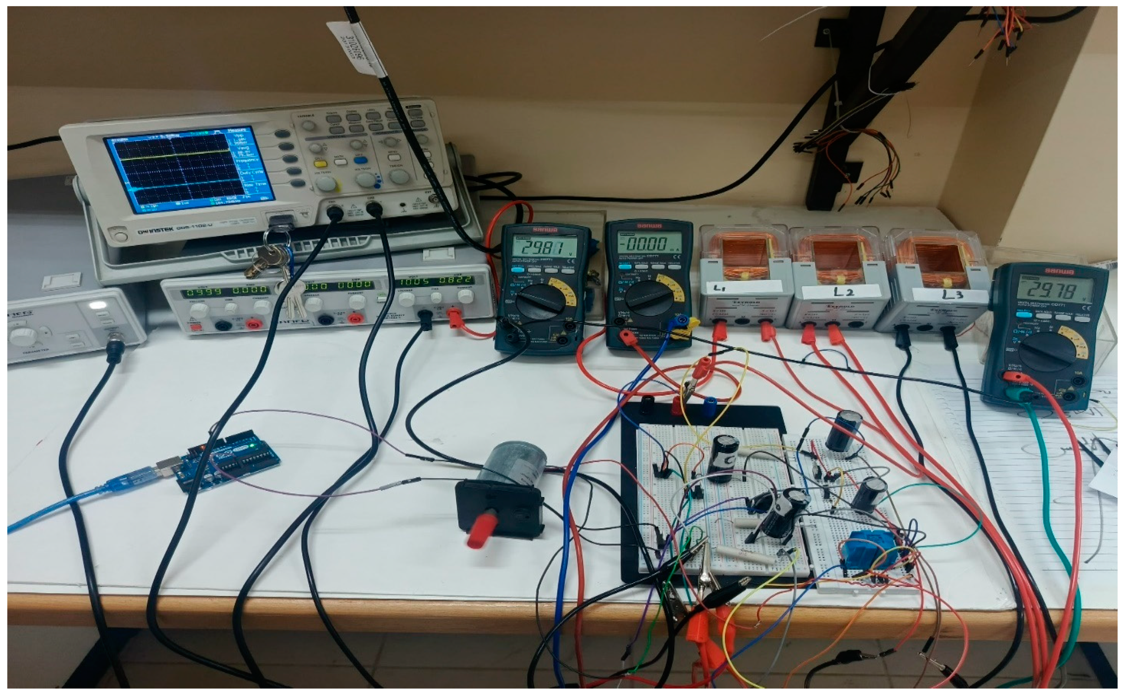
6. Experimental Implementation of the Proposed Regulator QDBC
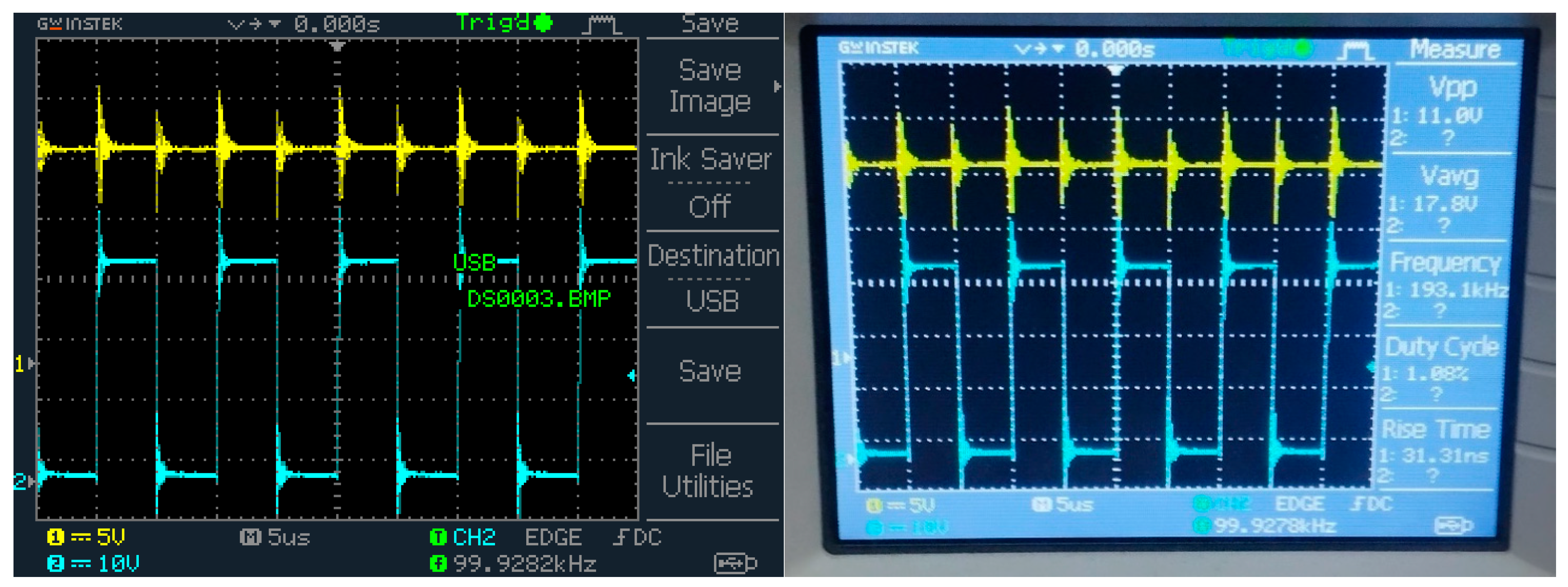
- An output voltage of 52 V (yellow) and output current of 1.5 A (blue) at a switching ratio when supplying a 12–34 V, 2400RPM High Speed Micro DC Motor;
- An output voltage of 92 V (yellow) and an output current of 1.8 A (blue) at a switching ratio when supplying a highly inductive resistive load of 3.3 mH and 200 Ω;
- An output voltage of 25 V (yellow) and an output current of 1.5 A (blue) at a switching ratio when supplying a highly inductive resistive load of 3.3 mH and 200 Ω.
- An output voltage of 52 V (yellow) and an output current of 1.5 A (blue);
- An output voltage of 91 V (yellow) and an output current of 1.8 A (blue);
- An output voltage of 26 V (yellow) and an output current of 1.5 A (blue).
7. Conclusions
Supplementary Materials
Author Contributions
Funding
Data Availability Statement
Acknowledgments
Conflicts of Interest
References
- Emar, W.A. Novel Enhanced High-Gain Quadruple-Diode Boost Regulator (QDBC) Setup for Solar Applications. Arab. J. Sci. Eng. 2024, 50, 5989–6016. [Google Scholar] [CrossRef]
- Alanazi, F. Electric Vehicles: Benefits, Challenges, and Potential Solutions for Widespread Adaptation. Appl. Sci. 2023, 13, 6016. [Google Scholar] [CrossRef]
- Ibrahim, M.; Rassõlkin, A.; Vaimann, T.; Kallaste, A. Overview on Digital Twin for Autonomous Electrical Vehicles Propulsion Drive System. Sustainability 2022, 14, 601. [Google Scholar] [CrossRef]
- Veerachary, M.; Kumar, N. Analysis and Design of Quadratic Following Boost Converter. IEEE Trans. Ind. Appl. 2020, 56, 6657–6673. [Google Scholar] [CrossRef]
- Kumar, M.; Panda, K.P.; Naayagi, R.T.; Thakur, R.; Panda, G. A Critical Analysis of Quadratic Boost Based High-Gain Converters for Electric Vehicle Applications: A Review. Sensors 2024, 24, 2186. [Google Scholar] [CrossRef] [PubMed]
- Anindya Sundar, J.; Lin, C.-H.; Kao, T.-H.; Chang, C.-H. A High Gain Modified Quadratic Boost DC-DC Converter with Voltage Stress Half of Output Voltage. Appl. Sci. 2022, 12, 4914. [Google Scholar] [CrossRef]
- Co, Y.-K.; Park, B.H.; Hyun, S.-B. Delta-Sigma Modulator-Based Step-Up DC-DC Converter with Dynamic Output Voltage Scaling. Electronics 2020, 9, 498. [Google Scholar] [CrossRef]
- Rezaie, M.; Abbasi, V. Effective combination of quadratic boost converter with voltage multiplier cell to increase voltage gain. IET Power Electron. 2020, 13, 2322–2333. [Google Scholar] [CrossRef]
- López-Santos, O.; Martínez-Salamero, L.; García, G.; Valderrama-Blavi, H.; Mercuri, D.O. Efficiency analysis of a sliding-mode controlled quadratic boost converter. IET Power Electron. 2013, 6, 364–373. [Google Scholar] [CrossRef]
- Walid, E.; Issa, H.; Kanaker, H.; Fares, O.; Attar, H. A New Double-Switch SEPIC-Buck Topology for Renewable Energy Applications. Energies 2024, 17, 238. [Google Scholar] [CrossRef]
- Fernão Pires, V.; Foito, D.; Cordeiro, A.; Silva, J.F. A Single-Switch DC/DC Buck/boost Converter with Extended Output Voltage. In Proceedings of the 7th International Conference on Renewable Energy Research and Applications (ICRERA), Paris, France, 14–17 October 2018; pp. 791–796. [Google Scholar] [CrossRef]
- Hart, D.W. Power Electronics, International ed.; McGraw-Hill: New York, NY, USA, 2011. [Google Scholar]
- Solis-Rodriguez, J.; Rosas-Caro, J.C.; Alejo-Reyes, A.; Valdez-Resendiz, J.E. Optimal Selection of Capacitors for a Low Energy Storage Quadratic Boost Converter (LES-QBC). Energies 2023, 16, 2510. [Google Scholar] [CrossRef]
- Emar, W. Hysteresis Current-Mode Regulated Modified SEPIC-Buck Converter Used for Solar Photovoltaic Systems. Arab. J. Sci. Eng. 2024, 49, 7053–7077. [Google Scholar] [CrossRef]
- Leyva-Ramos, J.; Mota-Varona, R.; Ortiz-Lopez, M.G.; Diaz-Saldierna, L.H.; Langarica-Cordoba, D. Control strategy of a quadratic boost converter with voltage multiplier cell for high-voltage gain. IEEE J. Emerg. Sel. Top. Power Electron. 2017, 5, 1761–1770. [Google Scholar] [CrossRef]
- Murad, Z.; Anzi, F.A.; Ben-Brahim, L. A Comparative Study of High-gain Cascaded DC-DC Converter Topologies. In Proceedings of the 3rd International Conference on Smart Grid and Renewable Energy (SGRE), Doha, Qatar, 20–22 March 2022; pp. 1–6. [Google Scholar] [CrossRef]
- Divya Navamani, J.; Boopathi, K.; Lavanya, A.; Vishnuram, P.; Bajaj, M.; Zaitsev, I. Low-capacitor stress reconfigurable quadratic boost converter with fault-tolerant capability for rooftop solar PV application. Sci. Rep. 2024, 14, 28269. [Google Scholar] [CrossRef]
- Ahmad, J.; Zaid, M.; Sarwar, A.; Lin, C.-H.; Ahmad, S.; Sharaf, M.; Zaindin, M.; Firdausi, M. A Voltage Multiplier Circuit Based Quadratic Boost Converter for Energy Storage Application. Appl. Sci. 2020, 10, 8254. [Google Scholar] [CrossRef]
- Sharma, P.; Hasanpour, S.; Kumar, R. Ultra-high voltage gain achieved with quadratic DC/DC converter design. Sci. Rep. 2024, 14, 23384. [Google Scholar] [CrossRef]
- Masoud, A.; Packnezhad, M.; Farzanehfard, H. A single-switch ultra-high step-up DC-DC converter with low voltage stress based on quadratic Y-sources topology. In Proceedings of the 14th Power Electronics, Drive Systems, and Technologies Conference (PEDSTC), Babol, Iran, 31 January–2 February 2023; pp. 1–6. [Google Scholar] [CrossRef]
- Hajilou, M.; Gholami, S.; Farzanehfard, H. Ultra-high step-up soft switched quadratic DC-DC converter with continuous input current and low switch voltage stress. In Proceedings of the 14th Power Electronics, Drive Systems, and Technologies Conference (PEDSTC) 2023, Babol, Iran, 31 January–2 February 2023; pp. 1–7. [Google Scholar]
- Silva-Vera, E.D.; Rosas-Caro, J.C.; Valdez-Resendiz, J.E.; Alejo-Reyes, A.; Ruiz-Martinez, O.F.; Posada Contreras, J.; García-Vite, P.M. Quadratic Boost Converter with Optimized Switching Ripple Based on the Selection of Passive Components. Electricity 2024, 5, 877–894. [Google Scholar] [CrossRef]
- Hidalgo, H.; Orosco, R.; Huerta, H.; Vázquez, N.; Hernández, C.; Pinto, S. A High-Voltage-Gain DC–DC Boost Converter with Zero-Ripple Input Current for Renewable Applications. Energies 2023, 16, 4860. [Google Scholar] [CrossRef]
- Samuel, V.J.; Keerthi, G.; Prabhakar, M. Ultra-high gain DC-DC converter based on interleaved quadratic boost converter with ripple-free input current. Int. Trans. Electr. Energ. Syst. 2020, 30, e12622. [Google Scholar] [CrossRef]
- Pang, Y.; Li, W.L.; Sun, H.X.; Pan, L.; Meng, F.T.; Liang, Y. High-Efficiency Multiphase Stacked Interleaved DC-DC Buck Converter with Very Low Output Current Ripple and Low Current–Voltage Stress. J. Electr. Eng. Technol. 2024, 19, 4969–4988. [Google Scholar] [CrossRef]
- Valarmathy, A.S.; Prabhakar, M. Non-isolated high gain DC–DC converter with ripple-free source current. Sci. Rep. 2024, 14, 973. [Google Scholar] [CrossRef] [PubMed]
- Hasanpour, S.; Siwakoti, Y.; Blaabjerg, F. New Single-Switch quadratic boost DC/DC converter with Low voltage stress for renewable energy applications. IET Power Electron. 2020, 13, 4592–4600. [Google Scholar] [CrossRef]
- Sharma, P.; Hasanpour, S.; Kumar, R. Enhanced Performance of Cuk and Boost–Based High-Gain Step-Up DC/DC Converter. Int. Trans. Electr. Energy Syst. 2024, 3166502, 18. [Google Scholar] [CrossRef]
- Emar, W.; Alzgool, M.; Mansour, I. Reliability Enhancement of a Double-Switch Single-Ended Primary Inductance–Buck Regulator in a Wind-Driven Permanent Magnet Synchronous Generator Using a Double-Band Hysteresis Current Controller. Energies 2024, 17, 4868. [Google Scholar] [CrossRef]
- Karimi Hajiabadi, M.; Lahooti Eshkevari, A.; Abdoli, I.; Mosallanejad, A.; Salemnia, A. A quadratic step-up DC-DC converter with high gain, reduced voltage stress, and component counts. Int. J. Circ. Theor. Appl. 2023, 51, 2186–2206. [Google Scholar] [CrossRef]
- Shi, T.; Wu, L.; Yan, Y.; Xia, C. Harmonic Spectrum of Output Voltage for Space Vector Pulse Width Modulated Ultra Sparse Matrix Converter. Energies 2018, 11, 390. [Google Scholar] [CrossRef]
- Wang, Y.; Duan, G.; Yu, J.; Yue, W.; Ning, J.; Liu, B. Harmonic Analysis of Sliding-Mode-Controlled Buck Converters Imposed by Unmodeled Dynamics of Hall Sensor. Energies 2023, 16, 6124. [Google Scholar] [CrossRef]
- Babaei, E.; Hosseini, S.H.; Gharehpetian, G.B. Reduction of THD and low order harmonics with symmetrical output current for single-phase AC/AC matrix converters. Int. J. Electr. Power Energy Syst. 2010, 32, 225–235. [Google Scholar] [CrossRef]
- Haque, M.A.; Niloy, M.A.; Khan, A.; Rahman, S.; Ahmed, I.; Jobair, A. Development of a Single-Phase Hybrid Quadratic AC-DC Boost Converter with Improved Power Quality. In Proceedings of the 10th IEEE International Conference on Power Systems (ICPS), Cox’s Bazar, Bangladesh, 13–15 December 2023; pp. 1–6. [Google Scholar] [CrossRef]
- Sharma, P.; Dhaked, D.K.; Saini, S.; Tripathi, L.K.; Shrivastva, A. Analysis of Different Converters for Reduced Total Harmonic Distortion and Improved Power Factor. In Proceedings of the 5th International Conference on Signal Processing and Integrated Networks (SPIN), Noida, India, 22–23 February 2018; pp. 608–613. [Google Scholar] [CrossRef]
- Julius, C.N.A.; Muhammad, L.N.; Daniyal, H.; Jaalam, N.; Abdullah, N.R.H.; Ab Ghani, S. A Comparative Study of Hysteresis current controller and PI regulator in Grid-Connected Inverter. Int. J. Adv. Trends Comput. Sci. Eng. 2019, 8, 3182–3187. [Google Scholar] [CrossRef]
- Goudarzian, A.; Khosravi, A.; Ali Raeisi, H. Optimized sliding mode current Converter for power converters with non-minimum phase nature. J. Frankl. Inst. 2019, 356, 8569–8594. [Google Scholar] [CrossRef]
- Maher, R.A.; Emar, W.; Jalil, A. Adaptive hysteresis-band controller. Int. J. Power Energy Convers. 2013, 4, 319–338. [Google Scholar] [CrossRef]
- Velázquez-Velázquez, J.-E.; Galván-Guerra, R.; Ortega-Pérez, J.-A.; Lozano-Hernández, Y.; Villafuerte-Segura, R. Finite-Time Current Tracking in Boost Converters by Using a Saturated Super-Twisting Algorithm. Complexity 2020, 7326157, 16. [Google Scholar] [CrossRef]
- Syed, S.A.; Khalid, H.A.; Farooq, H. Analysis and Efficiency Evaluation of Non-Isolated DC/DC Converter with Wide Input Voltage Range for PV Application. Eng. Proc. 2022, 20, 10. [Google Scholar] [CrossRef]
- Shrivastava, A.; Calhoun, B.H. Modeling DC-DC Converter Efficiency and Power Management in Ultra-Low Power Systems. In Proceedings of the Sub-Threshold Microelectronics Conference, Waltham, MA, USA, 9–10 October 2012. [Google Scholar]
- Chincholkar, S.; Tariq, M.; Urooj, S. Large-Signal Stability of the Quadratic Boost Converter Using a Disturbance Observer-Based Sliding-Mode Control. Mathematics 2023, 11, 3945. [Google Scholar] [CrossRef]


| QDBC Design Specifications | ||
|---|---|---|
| Parameter | Symbol | Real Value |
| Step Input Voltage | Vs | (50–100) V |
| Inductive choke with a series resistance (ESR) | L1 | 1 mH, 0.1 Ω |
| Inductive choke | L2 | 500 µH |
| Inductive choke with a series resistance (ESR) | L3 | 5 mH, 0.1 Ω |
| Capacitive filter | C1 | 1 mF |
| Capacitive filter | C2 | 470 μF |
| Capacitive filter | C3 | 470 μF |
| Capacitive filter | Co | 1 mF |
| Load resistance | Ro and Lo | 20 Ω and 2 mH |
| Switching frequency | f | 10 kHz |
| Forward diode voltage | - | 0.8 V |
| Parameter | Symbol | Real Value | Type |
|---|---|---|---|
| Step Input Voltage | Vs | (50–100) V | Power supply Haneef |
| Inductive choke | L1 | 2.3 mH | T-5817-10 interference inductive choke Treadmill 6 A inductance, Shenzhen, China |
| Inductive choke | L2 | 2.3 mH | T-5817-10 interference inductive choke Treadmill 6 A inductance, Shenzhen, China |
| Inductive choke | L3 | 2.2 mH | Leybold 56213, , 5 A, Shenzhen, China |
| Capacitive filter | C1 | 220 μF | Electrolytic Capacitive filter, 250 V, Shenzhen, China |
| Capacitive filter | C2 | 220 μF | Electrolytic Capacitive filter, 250 V, Shenzhen, China |
| Capacitive filter | C3 | 150 μF | Electrolytic Capacitive filter, 250 V, Shenzhen, China |
| Capacitive filter | Co | 470 μF | Electrolytic Capacitive filter, 250 V, Shenzhen, China |
| Load resistance | Ro and Lo | 250 W | PFC XT4800-1, Class B, Shenzhen, China |
| Diodes | D1 and D2 | F60UP60DN, Shanghai, China | |
| Diodes | D3 and D4 | F60UP20DN, Shanghai, China | |
| Transistor | MOSFET | IRFP260N, HEXFET, Power MOSFET, Shenzhen, China | |
| Switching frequency | f | 20 kHz | Arduino UNO, Shenzhen, China |
Disclaimer/Publisher’s Note: The statements, opinions and data contained in all publications are solely those of the individual author(s) and contributor(s) and not of MDPI and/or the editor(s). MDPI and/or the editor(s) disclaim responsibility for any injury to people or property resulting from any ideas, methods, instructions or products referred to in the content. |
© 2025 by the authors. Licensee MDPI, Basel, Switzerland. This article is an open access article distributed under the terms and conditions of the Creative Commons Attribution (CC BY) license (https://creativecommons.org/licenses/by/4.0/).
Share and Cite
Emar, W.; Aljanaideh, A.; Jaber, A.; Musleh, M.; Emar, A.; Al-Nairat, M. Delta Modulation Technique and Harmonic Analysis for the Modified Quadruple-Diode Boost Regulator Without and With a Voltage Multiplier Unit (VMU). Energies 2025, 18, 2492. https://doi.org/10.3390/en18102492
Emar W, Aljanaideh A, Jaber A, Musleh M, Emar A, Al-Nairat M. Delta Modulation Technique and Harmonic Analysis for the Modified Quadruple-Diode Boost Regulator Without and With a Voltage Multiplier Unit (VMU). Energies. 2025; 18(10):2492. https://doi.org/10.3390/en18102492
Chicago/Turabian StyleEmar, Walid, Ahmad Aljanaideh, Ala Jaber, Mohammad Musleh, Ali Emar, and Mohammed Al-Nairat. 2025. "Delta Modulation Technique and Harmonic Analysis for the Modified Quadruple-Diode Boost Regulator Without and With a Voltage Multiplier Unit (VMU)" Energies 18, no. 10: 2492. https://doi.org/10.3390/en18102492
APA StyleEmar, W., Aljanaideh, A., Jaber, A., Musleh, M., Emar, A., & Al-Nairat, M. (2025). Delta Modulation Technique and Harmonic Analysis for the Modified Quadruple-Diode Boost Regulator Without and With a Voltage Multiplier Unit (VMU). Energies, 18(10), 2492. https://doi.org/10.3390/en18102492