Article

A Stacked Symmetrical Non-Isolated High Step-Up Voltage Gain Converter with High Efficiency and Low Voltage Stress on Components

1
Institute of Mechatronics, Changwon National University, Changwon 51140, Republic of Korea
2
Department of Electrical Engineering, Changwon National University, Changwon 51140, Republic of Korea
*
Author to whom correspondence should be addressed.
Energies 2024, 17(7), 1668; https://doi.org/10.3390/en17071668
Submission received: 15 February 2024 / Revised: 24 March 2024 / Accepted: 29 March 2024 / Published: 31 March 2024

Abstract

:
This paper introduces a cascaded symmetrical non-isolated high step-up voltage gain converter with high efficiency and low voltage stress on components combining a non-isolated buck-boost converter and voltage doubler structure. In the proposed converter, the input source is connected in series to the output load; hence, a part of the source energy is directly delivered from source to load, not through the switching branch, improving efficiency. Furthermore, the appropriately stacked voltage doubler stage not only amplifies the high step-up voltage gain ratio but also considerably diminishes the voltage stress on all semiconductor devices and capacitors. As a result, the costless low internal resistance and low voltage components can be employed for higher efficiency, higher power density, and lower cost. To demonstrate the practicality of the proposed topology, the operating principle is outlined, and the steady-state characteristics are thoroughly analyzed. Furthermore, a 360 W prototype converter has been fabricated to confirm the efficiency of the proposed converter.

1. Introduction

Following the zero-carbon emission commitment of countries, renewable energy increasingly plays an important role in progressively dropping dependence on fossil fuels. Technically, renewable energy sources like fuel cells and solar cells generate direct current (DC) at low voltages, typically ranging between 25 V and 45 V [1,2]. Hence, employing a high voltage gain DC-DC converter to elevate the renewable source’s low voltage is crucial for supplying an appropriate DC link voltage to the subsequent DC-AC inverter, which uses 380 VDC for single-phase AC systems or 800 VDC for three-phase AC systems [3,4].
The simple solution that could be used is the isolated DC-DC converter topologies; however, it would not be a good option for small power systems in which volume and cost are critical factors. Traditional non-isolated DC-DC converters, like the non-isolated boost converter, are viable options for such applications. Nonetheless, its gain is capped due to the inductor’s parasitic components, and as the duty cycle nears one, the inductor’s current ripple and the power device’s hard-switch current increase, leading to substantial conduction and switching losses [1,2]. Furthermore, parasitic elements also introduce additional impedance and energy storage characteristics that can affect the overall performance and reliability of the system. Trace inductance, for example, can lead to undesired voltage spikes and ringing in the circuit due to the inductive energy stored during rapid changes in current. This can result in increased voltage stresses on components, potentially causing voltage breakdown or negatively impacting the lifespan of the devices. On the other hand, parasitic capacitances can affect the current stresses by introducing additional charge/discharge paths. This can lead to increased switching losses, higher power dissipation, and potential issues with signal integrity [5].
Over the past decade, numerous advanced boosting methods have been devised to surpass the constraints of traditional topologies. In [6], a new DC-DC converter with reduced inductor current was introduced to achieve a larger ratio of duty cycle to voltage gain and an inductor with a smaller current and reduced inductance. As a result, a smaller peak current is obtained. In general, the topologies can be categorized into multi-stage/interleaved boost converters, coupled-inductor-based topologies, switched capacitors, voltage doublers, and voltage lift techniques, each with distinct benefits and limitations [1,2].
The multi-stage [7,8,9], or interleaved boost converter [10,11,12], could be the first consideration. Reference [10] shows various configurations employing an interleaved boost converter with a clamped capacitor structure. Reference [11] detailed multiple interleaved boost converters integrated with voltage doubler cells. While these converters achieve high voltage gain, they are disadvantageous due to complex controls, component stress, larger volume, and hard-switching that lead to reduced efficiency [12].
Coupled inductor-based techniques, as in [13,14,15,16,17,18,19,20,21,22,23,24], seem to be a good choice. The voltage step-up gain is most dependent on the winding ratio. However, due to the voltage spike on the switch caused by leakage inductance, the external snubber is required, making the system complex and expensive. A further limitation of the coupled inductor-based topology is the excessive voltage stress on components, particularly those positioned after the coupled inductor’s second winding.
Non-magnetic coupling topologies, including the converters utilizing the switched capacitors (SCs) [25,26,27,28,29,30,31,32,33,34] and the voltage multiplier (VMs) [35,36,37,38,39], are also popular methods to achieve a high step-up ratio. Yet, converters utilizing SCs typically underperform regarding switch and capacitor voltage stresses due to the involvement of various voltages and the fact that most switches are not ground-referenced, complicating implementation. Another significant problem with SCs is the pulsating current caused by the charging and discharging of the capacitors. To address this issue, certain converters integrate SCs with additional magnetic components. The converter described in [28] merges two SCs with an energy storage (ES) cell. The pulsating current is mitigated, and the voltage stress on the switches is decreased. Unfortunately, the efficiency of this topology is low due to hard switching. Moreover, three large inductors need to be used, and the output capacitor is still stressed by the output voltage. As a result, the size and cost of this converter increase significantly. The converter mentioned in [29] improves efficiency, yet the voltage stress on components remains high, and control complexity increases due to the use of three main switches. While the converter in [30] achieves high voltage gain with a low-duty cycle, the high voltage stress on components and the notably low efficiency due to the absence of soft-switching techniques are significant drawbacks.
Similar to SC topology, converters with VMs benefit from the simplicity and ease of cascading for higher voltage gain, yet they primarily suffer from high stress on components and low efficiency [35,36,37,38]. The converter in [38] is structured to attain high gain with reduced component stress by symmetrically cascading voltage multipliers (VMs). However, its efficiency is not enhanced due to the persistence of hard-switching. Additionally, the voltage lift (VL) technique [40,41,42,43,44] is considered a promising approach for achieving high voltage gain. Luo introduced several lifting methods in [40], and various topologies based on these techniques have been proposed in [41,42,43,44,45,46,47,48]. However, this technique requires multiple inductors, which increases the circuit’s volume. Additionally, the stress on components remains high, particularly for those near the output side. To address the aforementioned issues, a proposed solution is a converter that achieves high efficiency and low voltage stress on all components.
The proposed converter is devised by attaching the positive and negative voltage doublers (VDs), as depicted in Figure 1a,b, to the upper and lower parts of the modified inverting buck-boost converter (m-IBB) shown in Figure 1a. The m-IBB converter’s output is serially linked with the capacitors of the voltage doublers, facilitating a substantial step-up in voltage gain. Moreover, this configuration reduces the voltage stress on all semiconductor devices and capacitors. A notable advantage is the enhanced power conversion efficiency since a part of input power is directly transferred to the load, not through switching devices. For even greater voltage gain, the design allows for simple expansion by adding more VDs at both the top and bottom of the m-IBB converter’s output. It should be noted that while having different grounds between input and output is a primary drawback, it does not significantly affect the complexity of the control design. This is because only one half-bridge MOSFET needs to be controlled, which can be easily addressed with a simple half-bridge gate driver with a bootstrap configuration.
This paper consists of five sections. Section 2 outlines the operating principles of the proposed converter. Section 3 details the design process for the proposed converter with two stages of the VDs. A comparative analysis of the proposed topology with other topologies is provided in Section 4. Section 5 discusses the experimental results to highlight the advantages of the proposed converter, culminating in a conclusion in Section 6.

2. Structure and Operating Principles

2.1. Structure

As shown in Figure 2, the proposed converter is constituted by four main parts: The modified synchronous inverting buck-boost is in the center as a source for N stages positive and negative voltage doublers (VDs) connected in series at both sides forming the symmetrical configuration. The Zero-Voltage Switching (ZVS) inductor in the common path of the positive and negative VDs is the main factor in achieving soft switching for all MOSFETs and diodes and eliminating the pulsating current caused by the source capacitor CP and CN of VDs. By connecting the output of m-IBB in series with its input, a higher step-up voltage gain can be achieved. Moreover, a part of power can be transferred directly from input to output, reducing losses and, hence, achieving higher efficiency. Furthermore, to attain an even higher voltage gain, the proposed converter can be readily extended by adding additional VDs in a cascading manner at both the top and bottom of the m-IBB output, all while maintaining the same voltage stress on components.

2.2. Working Principle

To simplify the working of the converter, the detailed analysis of the operation principle of the proposed converter is applied for only one stage of positive and negative VDs, and the voltage gain and voltage applied to components for N-stage VDs can be easily extended from a one-stage structure.
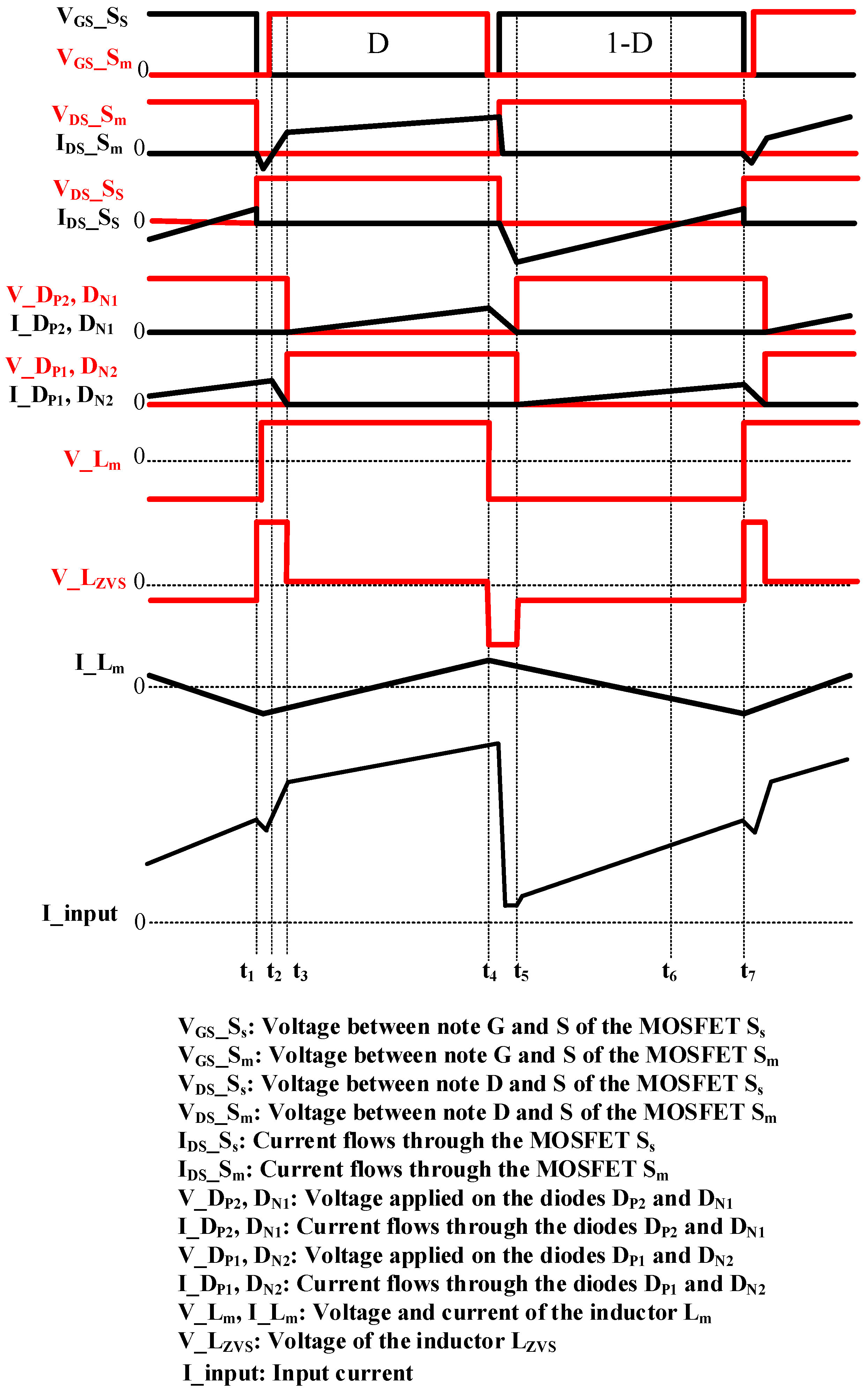
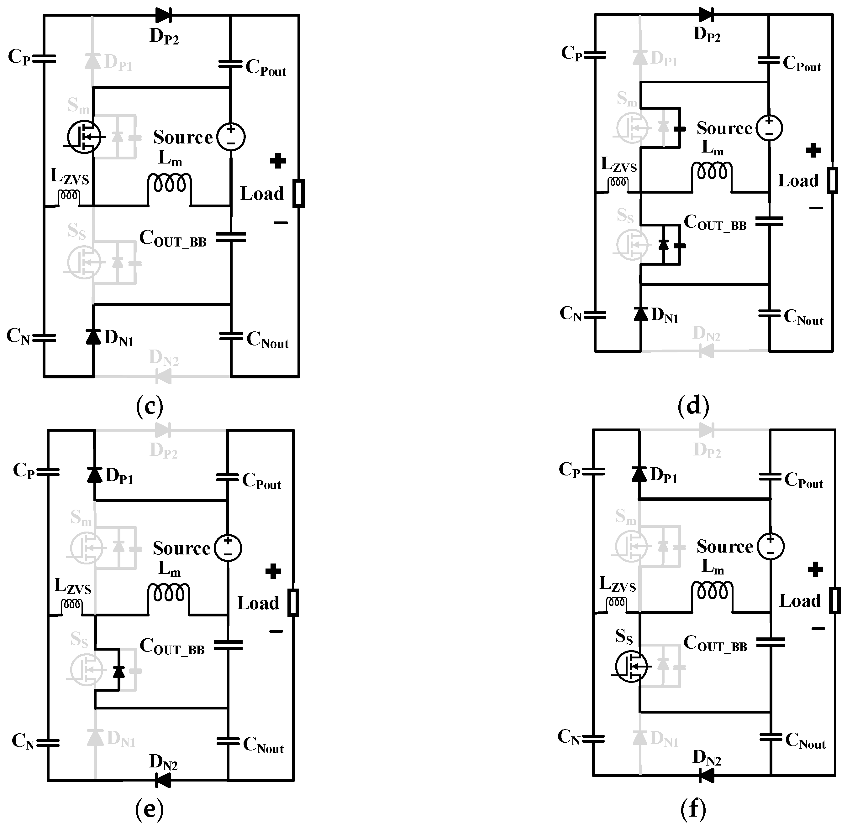
The operating principle of the proposed converter is examined in continuous conduction Mode (CCM), with the component operation waveforms depicted in Figure 3. One switching period of the proposed converter is segmented into six Modes, delineated by the status of the main switches of the m-IBB. The equivalent circuits for each Mode are illustrated in Figure 4. To elucidate the operating principle of the proposed converter, the following assumptions must be established:
  • All components are ideal, with parasitic components disregarded;
  • The circuit operates in a steady state with continuous inductor current;
  • All capacitors CP and CN have the same value;
  • All output capacitors CPout, CNout, and COUT_BB have the same value of Cout and are sufficiently large to keep their voltages constant during the switch-off period.
The switching period is Ts; switches close for a duration of DTs and open for (1−D)Ts.
(1) Mode 1 (t1–t2): ZVS Turn-On Condition for Main Switch Sm
Before that, the main switch Sm is off, and diodes DP1 and DN1 are reverse-biased. DP1 and DN2 are forward-biased. The synchronous switch SS is conducted through the main channel, not the body diode.
This Mode is started when SS switches off, the parasitic capacitor of SS is charged raising the voltage applied to this switch resulting in the discharge of the parasitic capacitor of the main switch Sm and reducing the voltage VDS applied to drain-source of Sm. Since the parasitic capacitor of Sm becomes fully discharged, the VDS of Sm will reach zero. Right the time the parasitic capacitor of Sm discharged totally, the ZVS inductor LZVS starts discharging and then changes its voltage polarity, leading to the forward bias of the body diode of Sm, then creating a ZVS turn-on for this main switch. At the end of this Mode, Sm switches on with ZVS condition.
(2) Mode 2 (t2–t3): ZCS (Zero-Current Switching) Turn-Off Condition for Diode DP2 and DP1
Sm is fully on, and the current flows through its main channel. Due to the discharging of ZVS inductor LZVS, the current flows through diode DP1 and DN2 decreases and reaches zero at the end of this Mode, forming a ZCS turn-off condition for these diodes.
V C P = V L m + V C oss _ Sm + V L Z V S + V S o u r c e
V C P + V L Z V S + V L m = V C O U T _ B B + V C N o u t + V C o s s _ S S
V O = V C P o u t + V C O U T _ B B + V C N o u t + V S o u r c e
(3) Mode 3 (t3–t4): Main Energy Transfer Mode
At the start of this Mode, Sm is on, SS is off. The main inductor Lm and ZVS inductor LZVS are storing energy. Diodes DP2 and DN1 are conducted, DP1 and DN2 are off, capacitors CN and CPout are charged, CP and COUT_BB are charged.
The output voltage Vo and voltage applied on components in this Mode can be expressed as follows.
V L m = V S o u r c e
V C P = V C P o u t + V L Z V S
V L m = V C N V C O U T _ B B + V L Z V S
V O = V C P o u t + V C O U T _ B B + V C N o u t + V S o u r c e
Since the current ILzvs is the combination of the current that flows through CPout and COUT_BB. Given that all the output capacitors are connected in series, and each has the same value as initially assumed, the current ILzvs flowing through the ZVS inductor Lzvs can be determined as expressed in Equation (8).
I L Z V S = 2 C P o u t Δ V o ( t 4 t 3 ) T s
Then, the voltage of ZVS inductor Lzvs can be calculated as in (9).
V L Z V S = L Z V S d i L Z V S d t = L Z V S 2 C P o u t Δ V o ( ( t 4 t 3 ) T s ) 2
(4) Mode 4 (t4–t5): ZCS Turn Off Condition for Diodes DP1 And DN2
At the start, Sm switches off, and SS switches on. The diodes DP1 and DN2 are reverse-biased, and DP2 and DP1 are forward-biased. SS is conducted via its body diode, the parasitic capacitor of SS is discharged, and that of Sm is charged. The main and ZVS inductors discharge, resulting in the decrement of the current through diodes DP2 and DP1 and creating ZCS turn-off for these diodes when the ZVS inductor LZVS is fully discharged.
The voltage equations in this Mode are given in (3).
V C P = V C P o u t + V C O S S _ S m + V L Z V S
V S o u r c e = V L m + V C O S S _ S m
V C N = V C O S S _ S S + V L Z V S
V C O S S _ S S = V L m + V C O U T _ B B
V O = V C P o u t + V C O U T _ B B + V C N o u t + V S o u r c e
(5) Mode 5 (t5–t6): Main Energy Transfer Mode
In this Mode, the energy accumulated in the inductor is released to the output capacitor COUT_BB, while the blocking capacitor CN of the negative VD discharges to the output capacitor CNout. Following its complete discharge in Mode 3, the secondary side ZVS inductor LZVS is recharged. Simultaneously, the blocking capacitor CP of the positive VD is charged in preparation for the next discharging cycle.
(6) Mode 6 (t6–t7): Main Energy Transfer Mode
At t = t6, as the voltage across capacitor COUT_BB rises above that of the main inductor, the body diode of SS becomes reverse-biased, causing the current to flow through SS rather than its body diode. By t = t7, the end of this Mode, one switching period concludes, setting the stage for the next cycle.
The output voltage and voltage applied on components in Modes 5 and 6 can be expressed as follows:
V L m = V C O U T _ B B
V L m = V S o u r c e V C P V L Z V S
V C N = V C N o u t + V L Z V S
V O = V C P o u t + V C O U T _ B B + V C N o u t + V S o u r c e
The same as in Mode 3, the current ILZVS flowing through the ZVS inductor LZVS can be calculated as in (19).
I L Z V S = 2 C P o u t Δ V o ( t 7 t 5 ) T s
Then, the voltage of inductors LZVS can be extracted as in (20)
V L Z V S = L Z V S d i L Z V S d t = 2 L Z V S C P o u t Δ V o ( ( t 7 t 5 ) T s ) 2

2.3. Steady-Stage Analysis of the Proposed Converter

2.3.1. Voltage Gain Expression

In the steady state, since Mode 1 occurs briefly, we can disregard these two Modes for steady-state analysis. Consequently, the period from t2 to t4 is DTS, and the period from t5 to t7 is (1 − D)TS. Applying the voltage-second principle of the inductor Lm, the average voltage across the inductor Lm in the switching period is zero, and the following equations can be obtained from (4)–(9) and (15)–(20).
V ¯ L m = D V S o u r c e ( 1 D ) V C O U T _ B B = 0
V ¯ L m = D V S o u r c e ( 1 D ) ( V S o u r c e V C P V L Z V S ) = 0
V ¯ L m = D ( V C N V C O U T _ B B + V L Z V S ) ( 1 D ) V C O U T _ B B = 0
V O = V C P o u t + V C N o u t + V C O U T _ B B + V S o u r c e
Then, the voltage of each capacitor can be obtained:
V C O U T _ B B = D V S o u r c e 1 D
V C N = V S o u r c e 1 D 2 L Z V S C N o u t Δ V o ( D T s ) 2
V C P = V S o u r c e 1 D 2 L Z V S C P o u t Δ V o ( ( 1 D ) T s ) 2
V C P o u t = V S o u r c e 1 D 2 L Z V S C P o u t Δ V o ( ( 1 D ) T s ) 2 2 L Z V S C P o u t Δ V o ( D T s ) 2
V C N o u t = V S o u r c e 1 D 2 L Z V S C N o u t Δ V o ( ( 1 D ) T s ) 2 2 L Z V S C N o u t Δ V o ( D T s ) 2
The voltage gain equation can be expressed as in (30).
V o = 3 V S o u r c e 1 D 4 L Z V S C Δ V o ( ( 1 D ) T S ) 2 4 L Z V S C Δ V o ( D T S ) 2
Furthermore, the ultra-high voltage gain can be easily achieved with the proposed converter by cascading more VD stages. It is important to ensure that the number of positive voltage doubler stages cascaded equals the number of negative voltage doubler stages, maintaining a symmetrical configuration. Assume that there are N stages of positive VDs and N stage negative VDs cascaded more. Theoretically, the cascaded voltage doubler stages function as a conventional voltage doubler, with the voltage output of each stage being twice that of its source. Then, the voltage output of N VD stages can be expressed as in (31).
V O T O T = ( 3 + 2 N ) V S o u r c e 1 D 4 L Z V S C Δ V O T O T ( ( 1 D ) T S ) 2 4 L Z V S C Δ V O T O T ( D T S ) 2

2.3.2. Voltage Stress on Components

In the proposed converter, it should be noted that the voltage across the switch and diodes are clamped by the capacitors. Consequently, low voltage stress can be attained for all semiconductor devices and passive components. Equation (25)–(29) demonstrates the voltage stress on all capacitors, while the stress on semiconductor devices is detailed in (32)–(34).
V S m = V S S = V S o u r c e 1 D
V D P 1 = V D P 2 = V C P = V S o u r c e 1 D 2 L Z V S C Δ V o ( ( 1 D ) T s ) 2 2 L Z V S C Δ V o ( D T s ) 2
V D N 1 = V D N 2 = V C N = V S o u r c e 1 D 2 L Z V S C Δ V o ( ( 1 D ) T s ) 2 2 L Z V S C Δ V o ( D T s ) 2
From (25)–(29) and (32)–(34), it is evident that the voltage stress on components is significantly lower than the output voltage and does not depend on it. This characteristic is a crucial advantage for high-gain step-up applications. For N-stage VDs cascaded, essentially, all the diodes and capacitors of the positive voltage doubler stages experience uniform voltage stress. In (33), the general voltage stress equation for diodes and capacitors of positive voltage doubler stages can be expressed.
Likewise, all the diodes and capacitors of the negative voltage doubler stages endure identical voltage stress, which can be detailed in (34).

2.3.3. ZVS Condition

From Mode 1, we know that, because of the discharging of inductor LZVS, the voltage VDS of switch Sm becomes zero while it is turning on. Then, the ZVS condition can be expressed as in (35).
V L Z V S V C P 0
Then, (35) can be expressed as follows.
L Z V S Δ I L Z V S ( t 7 t 5 ) T a V C P
where Ta is the time to inductor LZVS is fully discharged, and equal to the time of Mode 1 and Mode 2 (t3t1).
From (19) and (36), the value of inductor LZVS can be calculated as in (37).
L Z V S V C P T a Δ I L Z V S _ ( t 7 t 5 ) = V C P T a 2 C 1 Δ V o ( 1 D ) T s
It should be noted that, the current Δ I L Z V S _ ( t 7 t 5 ) represents the current circulating in the path including LZVS, CP, DP1 and Sm, as depicted in Figure 4a during Mode 1 and it causes some conduction loss during MOSFET switching. Therefore, its value should be kept small to minimize its contribution to the total losses of the converter. In this study, we opted for a design value of 0.5 A.

3. Design of the Proposed Converter

3.1. The ZVS Inductor Lzvs, Duty Cycle D, and Dead Time TD of Switches

Initially, it is necessary to determine a boundary for the duty cycle D, after which the boundary voltage of capacitor CP can be calculated. According to (30), the minimum duty cycle can be derived from the maximum output voltage when there is no effect of the ZVS inductor, as indicated in (38).
D min = 1 3 V s o u r c e V O
Next, we will calculate the value of inductors LZVS. From the (27), we see that when there is no inductor LZVS, the maximum voltage of capacitor CP is as follows. Then, we can calculate the maximum voltage of capacitor CP when duty cycle D is minimum, as shown in (39).
V C P _ max = V S o u r c e 1 D
From (38) and (39), we can calculate the boundary value of inductor LZVS with an assumption of discharging time Tr. Then, we can choose the value of inductor LZVS based on this boundary. After choosing the value for inductor LZVS, we need to calculate the right value for the duty cycle from (30). The dead time Td between the two switches must be smaller than the discharging time Tr of the inductor LZVS to maintain ZVS condition. In addition, the deadtime Td must be greater than total time taken for the rise and fall of the drain-source voltage of the MOSFETs to ensure the ZVS condition is maintained and to prevent the creation of a short circuit when the high-side MOSFET and low-side MOSFET of the half-bridge conduct simultaneously. This consideration can be determined from the data sheet of the MOSFETs and should be taken into account in the gate driver design.

3.2. Capacitor CP and CD

In Mode 1, when the switch Sm is activated but diode DP1 continues to conduct, the ZVS inductor LZVS resonates with the capacitor CP. To achieve the ZVS condition for Sm, the resonant frequency must be significantly lower than the switching frequency. Additionally, as previously assumed, the capacitors CP and CN are of equal value, which can be determined using (40).
C N = C P > > 1 ( 2 π f S ) 2 L Z V S

3.3. Main Inductor Design

The main inductors Lm are configured to ensure the proposed converter operates in CCM. Consequently, the values for inductor Lm can be calculated accordingly as in (41)
L m V S o u r c e D Δ I L m f S W
where Δ I L m is the current ripple of the main inductor Lm, f S W is the switching frequency.

3.4. Output Capacitor Design

The output capacitors can be determined based on the maximum output ripple voltage as (42).
C o u t I O D f S W × Δ V O
where I O is the output current
C o u t _ E q is the equivalent output capacitor, and can be calculated as (43).
C o u t _ E q = C P o u t C O U T _ B B C N o u t C P o u t C O U T _ B B + C O U T _ B B C N o u t + C P o u t C N o u t
Beginning from Section 2, we assumed that all the output capacitors are of the same value. Therefore, the value of these output capacitors can be calculated accordingly (44)
C P o u t = C N o u t = C O U T _ B B = 3 C o u t _ E q 3 I O D f S W × Δ V O

4. Experiment Results

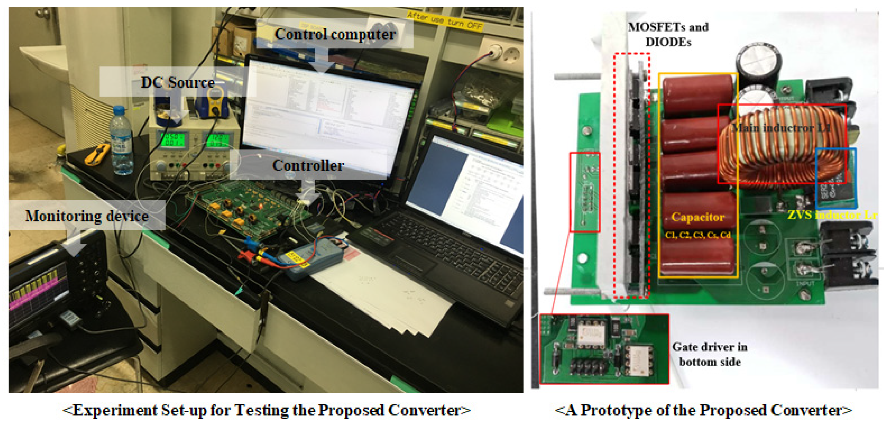
To verify the superiority of the proposed high step-up topology, a 360 W converter circuit with one stage of VDs is built and tested as in Figure 5 with the specification and used components shown in Table 1 and Table 2.
In the experiments, the MCU STM32G431CBT3, a product of STMicroelectronics and sourced from Seoul, South Korea, is used for controlling. The maximum duty cycle of the Sm in full load is 0.73 to boost the input voltage from 40 V to the output voltage of 380 V. The dead time between the two switches is 100 ns.
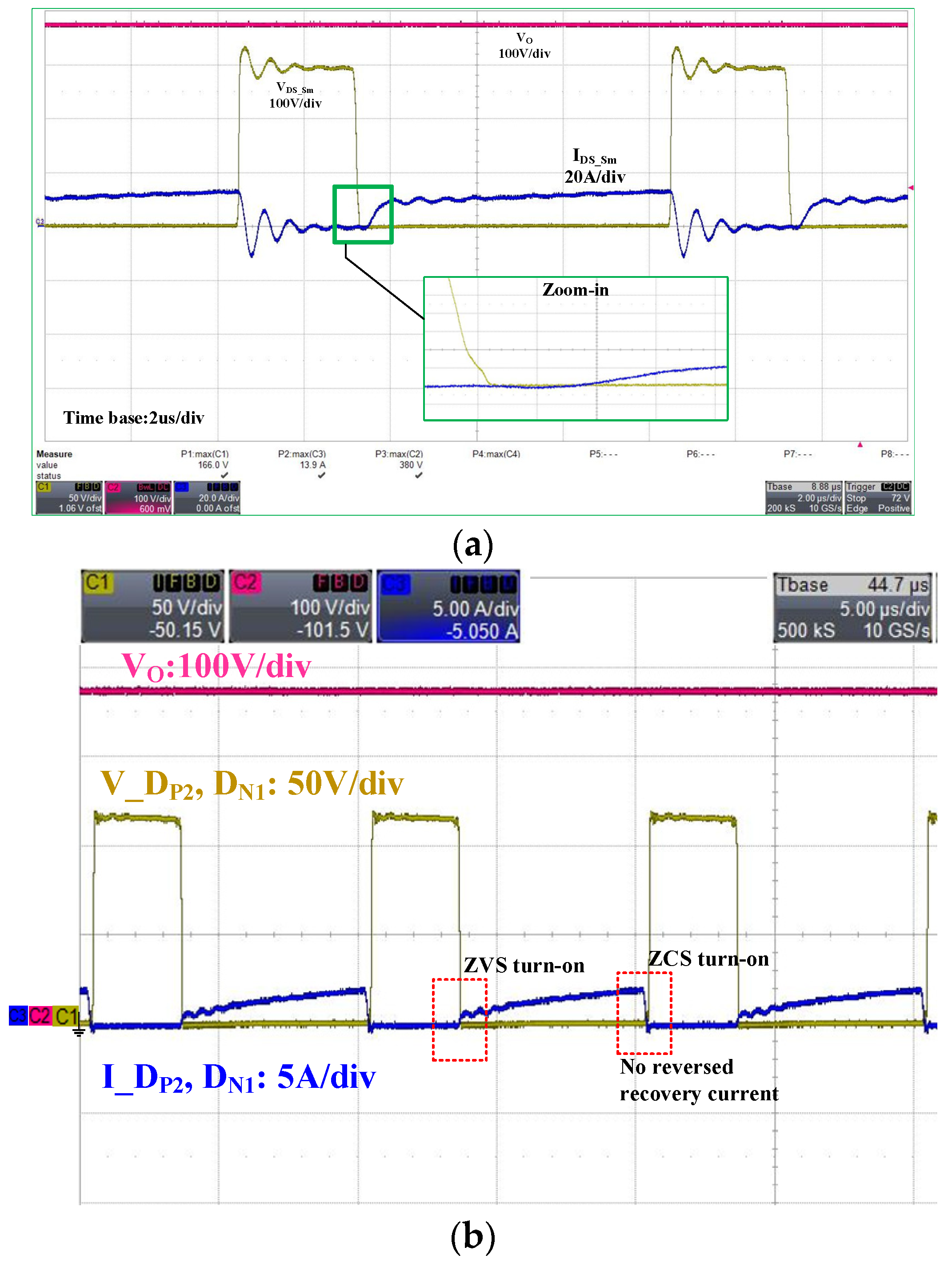
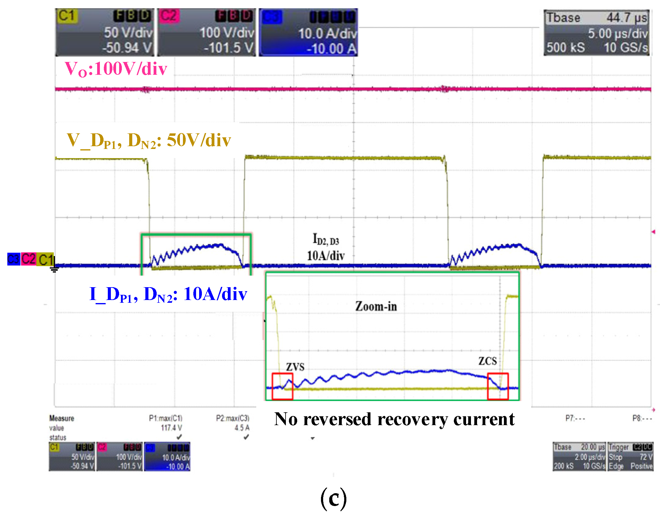
Figure 6 shows the experimental waveform of all the switches and diodes. As seen in Figure 6a, it is evident that the main MOSFET Sm is turned on with the ZVS condition. Additionally, Figure 6b,c show the voltage and current waveforms for diodes. It is obvious that all the diodes are switched on with ZVS and turned off with ZCS condition. Although there is a small ringing in current through the diode caused by the parasitic components and PCB layout, soft switching is achieved for all switches and diodes.
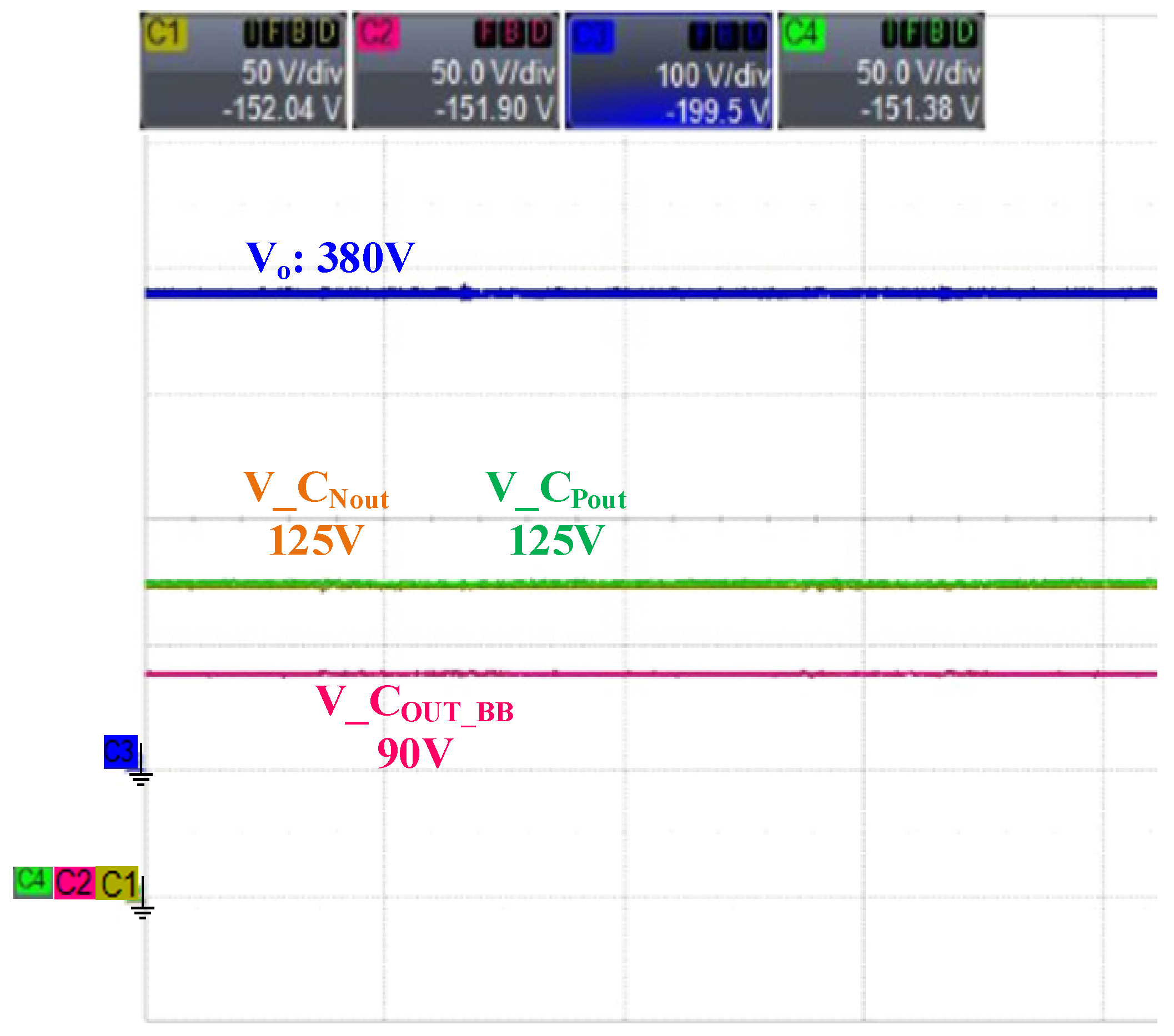
Figure 7 illustrates the voltage across the output capacitors, which, due to the symmetrical configuration, is considerably lower compared to other topologies.
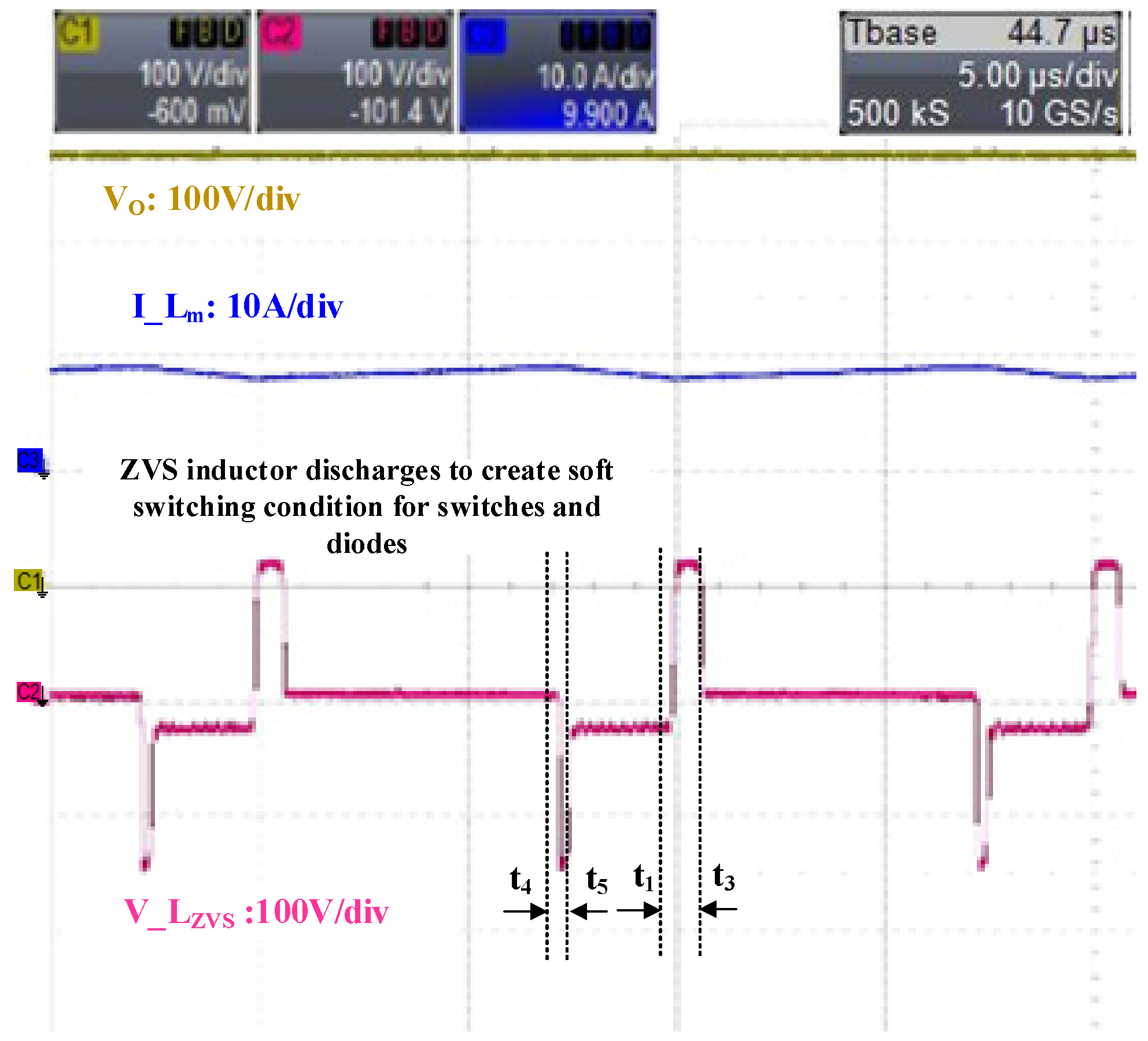
Figure 8 presents the waveforms of the main inductor current ILZVS and the voltage waveform of the ZVS inductor VLZVS at full load, closely aligning with the simulation results. It is clear that the ZVS inductor LZVS fully discharges in a brief period when the switch Sm turns on, fulfilling the requirement for the ZVS condition to occur.
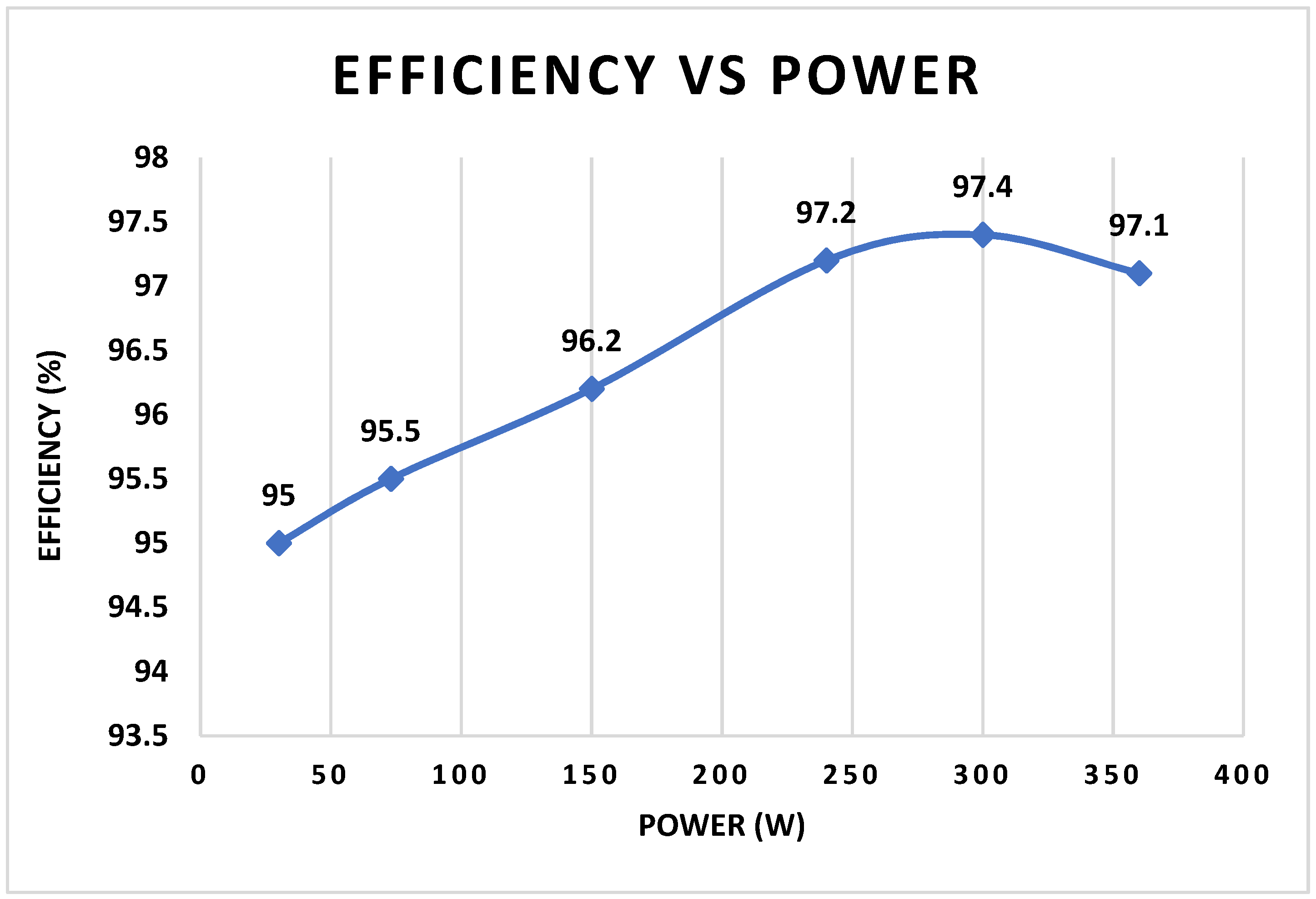
Figure 9 displays the efficiency plot for the proposed converter varies to the output power with input parameters of VSource = 40 V, VO = 380 V, and a switching frequency of 100 kHz. As indicated in Figure 9, the efficiency varies from above 95% at light load to over 97% at heavy load, with a peak efficiency of 97.4% achieved at 295 W.
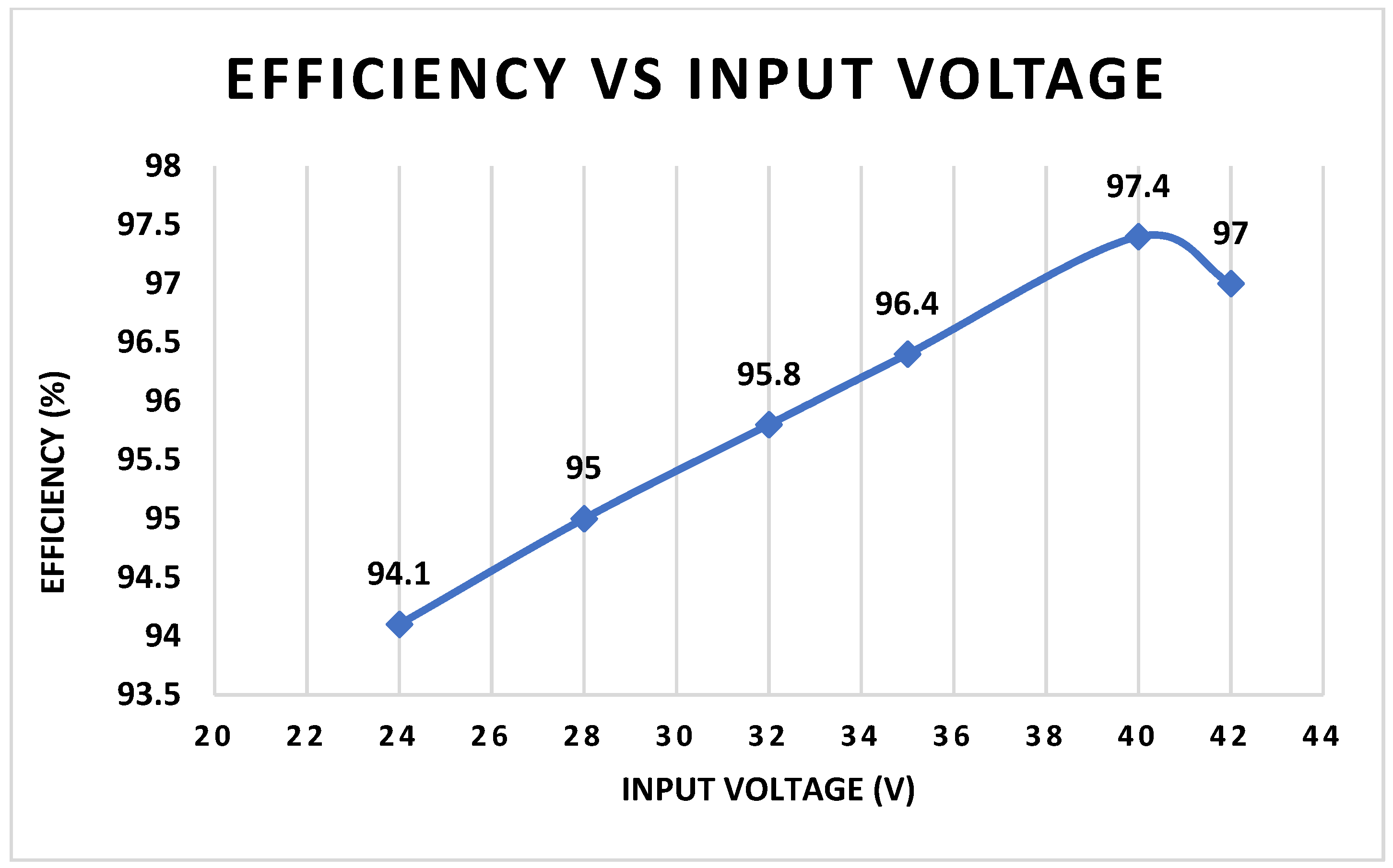
Figure 10 displays the efficiency plot for the proposed converter varying with the input voltage, with input parameters set to output power = 300 W, VO = 380 V, and a switching frequency of 100 kHz. As indicated in Figure 10, the efficiency ranges from above 94.1% at an input voltage of 24 V to over 97% at an input voltage of 42 V, reaching a peak efficiency of 97.4% at an input voltage of 40 V.

5. Detailed Comparison and Discussion

From Table 3, we can see that the proposed converter achieves higher efficiency and lower voltage stress on components, especially on the output side components, while maintaining a high step-up gain.
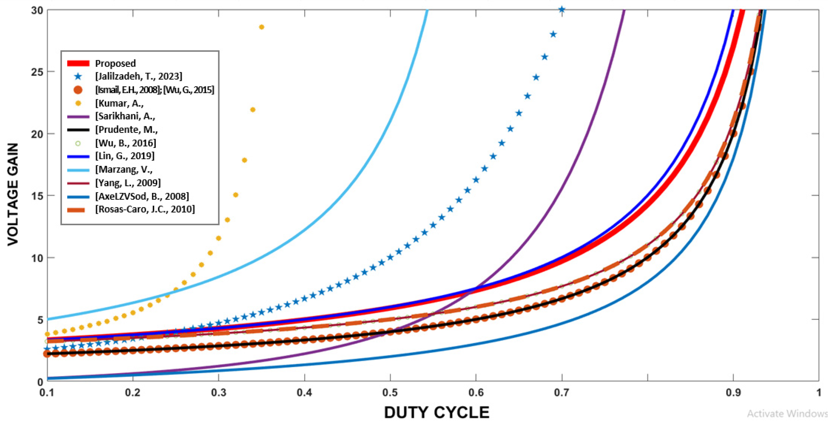
As shown in Figure 11, the converters in (28), (29), (30), (9), (12) have higher voltage gain than the proposed topology. However, they also have their drawbacks.
Even though the converters in [9,12] use fewer components, the efficiency is lower due to hard switching for semiconductor components. Furthermore, the voltage stress on components on the output side is significantly high, and they both need to use two large inductors that make the volume of the circuit increase.
The converter in [28] employs three larger inductors, which results in increased volume and cost. Furthermore, the voltage stress on most components is higher compared to that in the proposed converter, and the efficiency is lower than that of our converter.
The converter in [29] utilizes three active switches and two main inductors, leading to complexity in control and an increased volume. Additionally, the voltage stress on components is higher, and the efficiency is lower compared to the proposed converter. Another significant drawback of this converter is the elevated voltage stress on components, particularly on the output-side components, compared to the proposed topology.
The converter in [30] boasts high gain with a low-duty cycle as its advantage. However, its efficiency is considerably lower compared to ours. Moreover, there is still a notable issue of high and uneven voltage stress on the components. Components near the output side, such as output diode DO, output capacitor CO, and capacitors C2 and C3, experience particularly high voltage stress.
The converter in [34] achieves a similar voltage gain and voltage stress on components (switches and diodes) with a lower component count. However, it operates with hard switching, leading to low efficiency and high volume due to the necessity of using a low switching frequency.
The converter in [39] (Figure 4) appears to achieve a higher voltage with a certain number of voltage multiplier stages compared to the proposed converter, and its efficiency is high. However, it requires the use of many components, and a low frequency is implemented since no soft switching is employed, resulting in high volume and cost. It should be noted that the proposed converter will significantly increase voltage gain by cascading more voltage doubler stages, making the design process simpler and more practical.
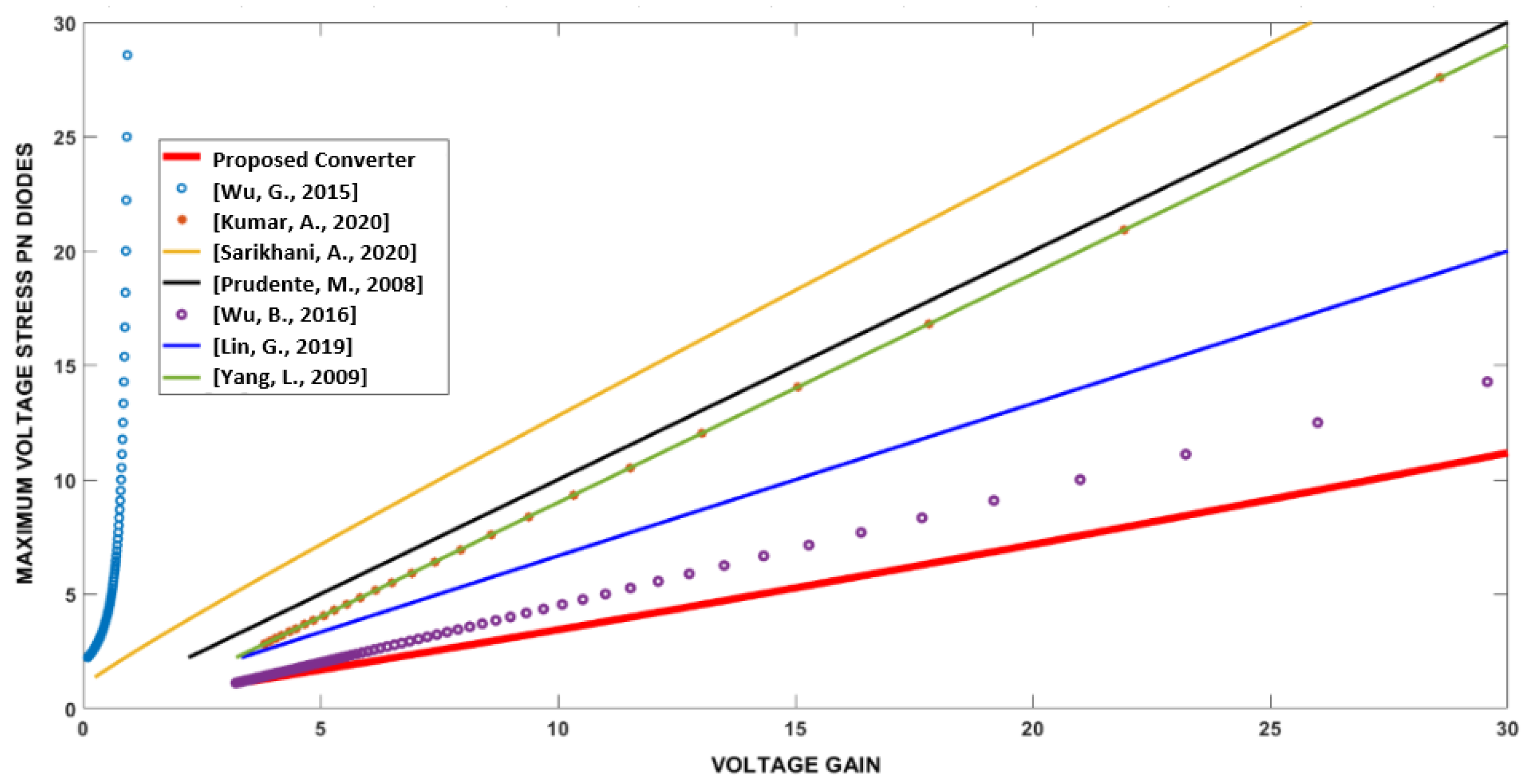
Figure 12 illustrates the variation in maximum voltage stress on diodes with voltage gain. The proposed converter exhibits the lowest voltage stress on diodes compared to the other converters.
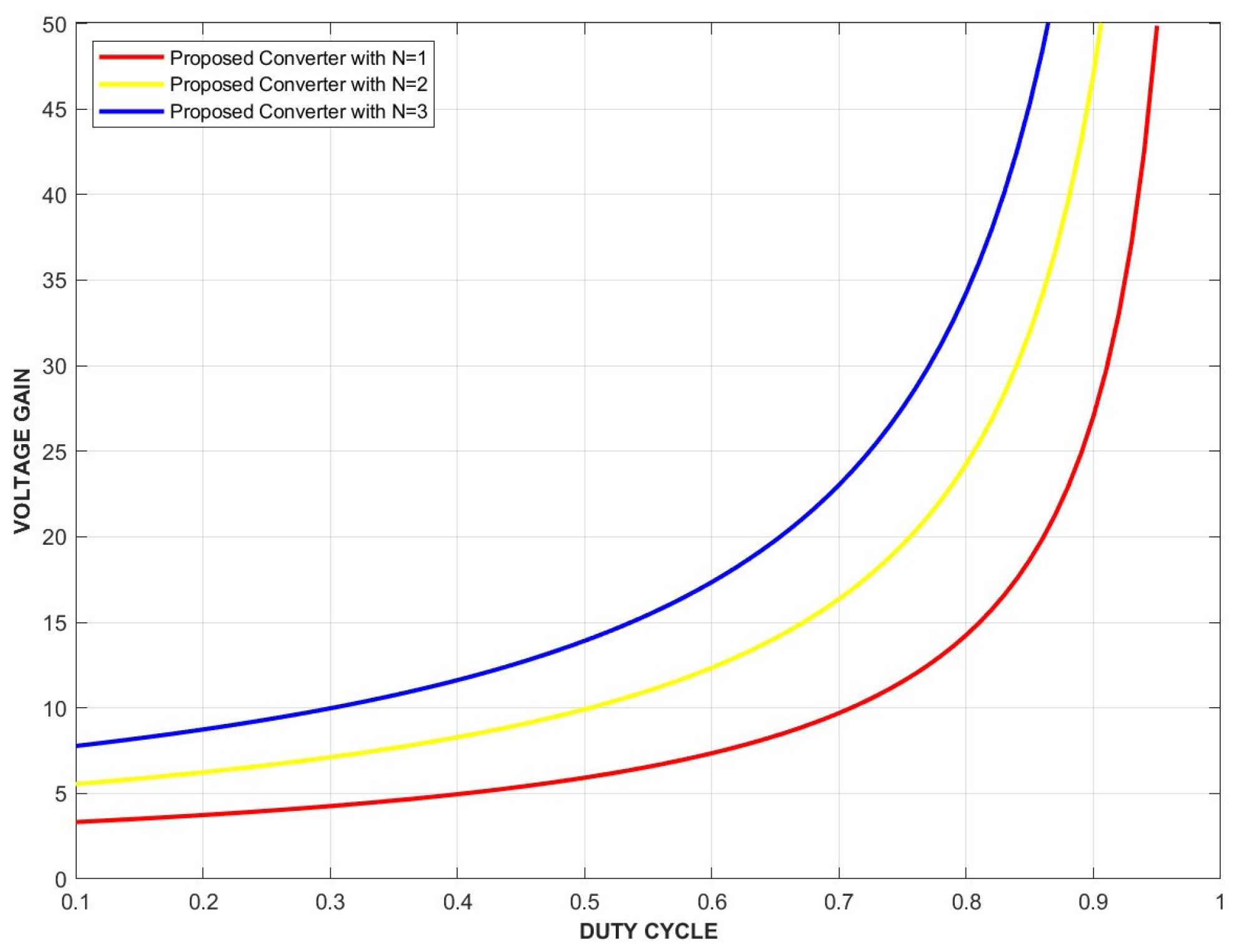
Figure 13 shows the voltage gain of the proposed converter with one, two, and three stages of the cascaded voltage doubler. It can be seen that the proposed converter can easily obtain ultra-high gain flexibly by cascading more VD stages or using higher-duty cycles.
It is important to note that, as discussed in Part II, when cascading more VD stages, the voltage stress on components is not affected. In fact, it will be lower since the voltage stress on components only depends on the source voltage and the duty cycle. If cascading more VD stages, it could obtain a higher gain with a low-duty cycle, consequently reducing the voltage stress on components.
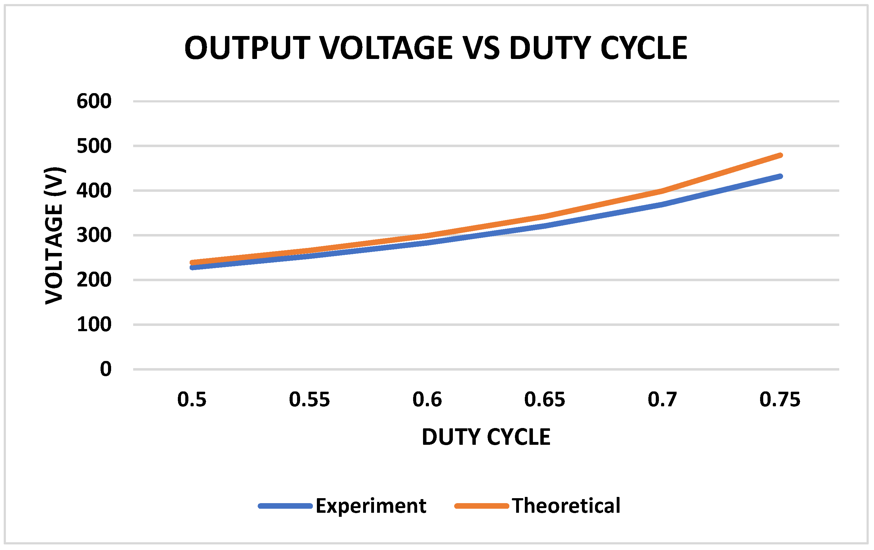
Figure 14 shows the accuracy of the simplified theoretical analysis in (30) in comparison to the experimental results with an input voltage of 40 V, output power of 300 W. It can be seen that the accuracy of the theoretical analysis in (30) decreases with the increase of duty cycle. This is attributed to the growing influence of parasitic components, which become more dominant at higher duty cycles.

6. Conclusions

This paper presents a non-isolated high step-up boost converter designed for low voltage stress on components and high efficiency while maintaining a high step-up voltage gain. Its effectiveness and practicality have been validated through experiments with a 360 W prototype converter. Compared to other non-isolated high voltage gain boost converters, this proposed converter achieves a relatively high voltage gain with a maximum efficiency of 97.4%. It also ensures significantly lower voltage stress on switches and passive components than other high voltage gain non-isolated converters. An added benefit is the ability to further increase the voltage gain by simply adding more voltage doublers. However, the input and output do not share a common ground, and pulsating input current remains a disadvantage of this converter. In the future, further studies will be conducted to optimize the design, perform comprehensive analysis, and explore specific applications of the proposed converter.
This converter is ideally suited for distributed power generation systems utilizing renewable energy sources that require high voltage gain without the need for a transformer.

Author Contributions

Project administration, writing—review and editing, M.-C.D.; writing—original draft preparation, T.-T.L.; Supervision, M.P. All authors have read and agreed to the published version of the manuscript.

Funding

This research was supported by Basic Science Research Program through the National Research Foundation of Korea (NRF) funded by the Ministry of Education (RS-2023-00246086).

Data Availability Statement

The original contributions presented in the study are included in the article, further inquiries can be directed to the corresponding author.

Conflicts of Interest

The authors declare no conflicts of interest.

References

  1. Li, W.; He, X. Review of nonisolated high-step-up dc/dc converters in photovoltaic grid-connected applications. IEEE Trans. Ind. Electron. 2011, 58, 1239–1250. [Google Scholar] [CrossRef]
  2. Forouzesh, M.; Siwakoti, Y.P.; Gorji, S.A.; Blaabjerg, F.; Lehman, B. Step-Up DC–DC Converters: A Comprehensive Review of Voltage-Boosting Techniques, Topologies, and Applications. IEEE Trans. Power Electron. 2017, 32, 9143–9178. [Google Scholar] [CrossRef]
  3. Gupta, A.; Korada, N.; Ayyanar, R. Quadratic-Extended-Duty-Ratio Boost Converters for Ultra High Gain Application with Low Input Current Ripple and Low Device Stress. IEEE Trans. Ind. Appl. 2023, 59, 938–948. [Google Scholar] [CrossRef]
  4. Hsieh, Y.; Chen, J.; Liang, T.; Yang, L. Novel high step-up dc–dc converter for distributed generation system. IEEE Trans. Ind. Electron. 2013, 60, 1473–1482. [Google Scholar] [CrossRef]
  5. Górecki, P.; d’Alessandro, V. A Datasheet-Driven Electrothermal Averaged Model of a Diode–MOSFET Switch for Fast Simulations of DC–DC Converters. Electronics 2024, 13, 154. [Google Scholar] [CrossRef]
  6. Rosas-Caro, J.C.; Valdez-Resendiz, J.E.; Escobar, G.; Beltran-Carbajal, F. A Multilevel Boost Converter with Reduced Inductor Current. Electronics 2023, 12, 4585. [Google Scholar] [CrossRef]
  7. Amiri, E.M.; Moghani, J.S.; Gharehpetian, G.B.; Yazdi, S.S.H. Novel two stage buck-boost converter with zero-voltage transition operation. In Proceedings of the 5th Annual International Power Electronics, Drive Systems and Technologies Conference (PEDSTC 2014), Tehran, Iran, 5–6 February 2014; pp. 143–147. [Google Scholar]
  8. Aamir, M.; Shinwari, M.Y. Design, implementation and experimental analysis of two-stage boost converter for grid connected photovoltaic system. In Proceedings of the 3rd International Conference on Computer Science and Information Technology, Chengdu, China, 9–11 July 2010; pp. 194–199. [Google Scholar]
  9. Sarikhani, A.; Allahverdinejad, B.; Hamzeh, M. A Non-Isolated Buck-Boost DC-DC Converter with Continuous Input Current for Photovoltaic Applications. IEEE J. Emerg. Sel. Top. Power Electron. 2020, 8, 804–811. [Google Scholar]
  10. Zeng, Y.; Li, H.; Wang, W.; Zhang, B.; Zheng, T.Q. High Efficient High Voltage Gain Capacitor Clamped DC-DC Converters and Its Construction Method. IEEE Trans. Ind. Electron. 2020, 68, 3992–4003. [Google Scholar] [CrossRef]
  11. Alzahrani, A.; Ferdowsi, M.; Shamsi, P. A Family of Scalable Non-Isolated Interleaved DC-DC Boost Converters with Voltage doubler Cell. IEEE Access 2019, 7, 11707–11721. [Google Scholar] [CrossRef]
  12. Lin, G.; Zhang, Z. Low Input Ripple High Step-Up Extendable Hybrid DC-DC Converter. IEEE Access 2019, 7, 158744–158752. [Google Scholar] [CrossRef]
  13. Wu, T.; Lai, Y.; Hung, J.; Chen, Y. Boost converter with coupled inductors and buck–boost type of active clamp. IEEE Trans. Ind. Electron. 2008, 55, 154–162. [Google Scholar] [CrossRef]
  14. Wai, R.; Lin, C. High-efficiency, high-step-up dc–dc converter for fuel-cell generation system. IEEE Proc. Elect. Power Appl. 2005, 152, 1371–1378. [Google Scholar] [CrossRef]
  15. Hsieh, Y.P.; Chen, J.F.; Yang, L.S.; Wu, C.Y.; Liu, W.S. High conversion-ratio bidirectional DC/DC converter with couple inductor. IEEE Trans. Ind. Electron. 2014, 61, 1311–1319. [Google Scholar] [CrossRef]
  16. Chen, S.M.; Liang, T.J.; Yang, L.S.; Chen, J.F. A boost converter with capacitor multiplier and coupled inductor for ac module applications. IEEE Trans. Ind. Electron. 2013, 60, 1503–1511. [Google Scholar] [CrossRef]
  17. Das, M.; Agarwal, V. Design and Analysis of a High-Efficiency DC–DC Converter with Soft Switching Capability for Renewable Energy Applications Requiring High Voltage Gain. IEEE Trans. Ind. Electron. 2016, 63, 2936–2944. [Google Scholar] [CrossRef]
  18. Molavi, N.; Adib, E.; Farzanehfard, H. Soft-switched non-isolated high step-up DC–DC converter with reduced voltage stress. IET Power Electron. 2016, 9, 1711–1718. [Google Scholar] [CrossRef]
  19. Kumar, A.; Peri, R.; Kundu, U.; Sensarma, P. A high voltage gain current fed non-isolated dc-dc converter. In Proceedings of the 2016 IEEE International Conference on Power Electronics, Drives and Energy Systems (PEDES), Trivandrum, India, 14–17 December 2016; pp. 1–6. [Google Scholar]
  20. Hassan, W.; Lu, D.D.; Xiao, W. Analysis and experimental verification of a single-switch high-voltage gain ZCS DC–DC converter. IET Power Electron. 2019, 12, 2146–2153. [Google Scholar] [CrossRef]
  21. Zaoskoufis, K.; Tatakis, E.C. An Improved Boost-based DC/DC Converter with High Voltage step-up ratio for DC Microgrids. IEEE J. Emerg. Sel. Top. Power Electron. 2021, 9, 1837–1853. [Google Scholar] [CrossRef]
  22. Chen, M.; Yin, C.; Loh, P.C.; Ioinovici, A. Improved Large DC Gain Converters with Low Voltage Stress on Switches Based on Coupled-Inductor and Voltage doubler for Renewable Energy Applications. IEEE J. Emerg. Sel. Top. Power Electron. 2020, 8, 2824–2836. [Google Scholar] [CrossRef]
  23. Mohseni, P.; Hosseini, S.H.; Maalandish, M. A New Soft Switching DC-DC Converter with High Voltage Gain Capability. IEEE Trans. Ind. Electron. 2020, 67, 7386–7398. [Google Scholar] [CrossRef]
  24. Liu, T.; Lin, M.; Ai, J. High Step-Up Interleaved DC-DC Converter with Asymmetric Voltage Multiplier Cell and Coupled Inductor. IEEE J. Emerg. Sel. Top. Power Electron. 2020, 8, 4209–4222. [Google Scholar] [CrossRef]
  25. Ismail, E.H.; Al-Saffar, M.A.; Sabzali, A.J.; Fardoun, A.A. A family of single-switch PWM converters with high step-up conversion ratio. IEEE Trans. Circuits Syst. I Reg. Pap. 2008, 55, 1159–1171. [Google Scholar] [CrossRef]
  26. Wu, G.; Ruan, X.; Ye, Z. Nonisolated High Step-Up DC–DC Converters Adopting Switched-Capacitor Cell. IEEE Trans. Ind. Electron. 2015, 62, 383–393. [Google Scholar] [CrossRef]
  27. Tran, V.-T.; Nguyen, M.-K.; Choi, Y.-O.; Cho, G.-B. Switched-Capacitor-Based High Boost DC-DC Converter. Energies 2018, 11, 987. [Google Scholar] [CrossRef]
  28. Jalilzadeh, T.; Rostami, N.; Babaei, E.; Maalandish, M. Non-Isolated Topology for High Step-Up DC-DC Converters. IEEE J. Emerg. Sel. Top. Power Electron. 2023, 11, 1154–1168. [Google Scholar] [CrossRef]
  29. Marzang, V.; Hosseini, S.H.; Rostami, N.; Alavi, P.; Mohseni, P.; Hashemzadeh, S.M. A High Step-Up Non-Isolated DC-DC Converter with Flexible Voltage Gain. IEEE Trans. Power Electron. 2020, 35, 10489–10500. [Google Scholar] [CrossRef]
  30. Kumar, A.; Wang, Y.; Pan, X.; Raghuram, M.; Singh, S.K.; Xiong, X.; Tripathi, A.K. Switched-LC based High Gain Converter with Lower Component Count. IEEE Trans. Ind. Appl. 2020, 56, 2816–2827. [Google Scholar] [CrossRef]
  31. Ye, Y.; Cheng, K.W.E. A Family of Single-Stage Switched-Capacitor–Inductor PWM Converters. IEEE Trans. Power Electron. 2013, 28, 5196–5205. [Google Scholar] [CrossRef]
  32. Li, S.; Zheng, Y.; Wu, B.; Smedley, K.M. A Family of Resonant Two-Switch Boosting Switched-Capacitor Converter with ZVS Operation and a Wide Line Regulation Range. IEEE Trans. Power Electron. 2018, 33, 448–459. [Google Scholar] [CrossRef]
  33. Salvador, M.A.; De Andrade, J.M.; Lazzarin, T.B.; Coelho, R.F. Non-isolated High-Step-Up DC-DC Converter Derived from Switched-Inductors and Switched-Capacitors. IEEE Trans. Ind. Electron. 2020, 67, 8506–8516. [Google Scholar] [CrossRef]
  34. Mohammadi, F.; Gharehpetian, G.B. Rastegar and M. Farhadi-Kangarlu. Non-isolated Step-up DC-DC Converter Based on Switched Capacitor Cells. CSEE J. Power Energy Syst. 2023, 9, 1161–1172. [Google Scholar]
  35. Prudente, M.; Pfitscher, L.L.; Emmendoerfer, G.; Romaneli, E.F.; Gules, R. Voltage doubler Cell Applied to Non-Isolated DC–DC Converters. IEEE Trans. Power Electron. 2008, 23, 871–887. [Google Scholar] [CrossRef]
  36. Alcazar, Y.J.A.; de Souza Oliveira, D.; Tofoli, F.L.; Torrico-Bascopé, R.P. DC–DC Nonisolated Boost Converter Based on the Three-State Switching Cell and Voltage doubler Cell. IEEE Trans. Ind. Electron. 2013, 60, 4438–4449. [Google Scholar] [CrossRef]
  37. Prudente, M.; Pfitscher, L.; Gules, R. A Boost Converter with Voltage doubler Cell. In Proceedings of the 2005 IEEE 36th Power Electronics Specialists Conference, Dresden, Germany, 16 June 2005; pp. 2716–2721. [Google Scholar]
  38. AxeLZVSod, B.; Golan, G.; Berkovich, Y.; Shenkman, A. Diode–capacitor voltage doublers combined with boost-converters: Topologies and characteristics. IET Power Electron. 2012, 5, 873–884. [Google Scholar]
  39. Feretti, P.H.; Tofoli, F.L.; Ribeiro, E.R. Family of Non-Isolated High Step-Up DC–DC Converters Based on the Multi-State Switching Cell. IEEE J. Emerg. Sel. Top. Power Electron. 2022, 10, 5882–5893. [Google Scholar] [CrossRef]
  40. Wu, B.; Li, S.; Liu, Y.; Smedley, K.M. A New Hybrid Boosting Converter for Renewable Energy Applications. IEEE Trans. Power Electron. 2016, 31, 1203–1215. [Google Scholar] [CrossRef]
  41. Luo, F.L.; Ye, H. Positive output super-lift converters. IEEE Trans. Power Electron. 2003, 18, 105–113. [Google Scholar]
  42. Sayed, S.; Elmenshawy, M.; Elmenshawy, M.; Ben-Brahim, L.; Massoud, A. Design and analysis of high-gain medium-voltage DC-DC converters for high-power PV applications. In Proceedings of the 2018 IEEE 12th International Conference on Compatibility, Power Electronics and Power Engineering (CPE-POWERENG 2018), Doha, Qatar, 10–12 April 2018; pp. 1–5. [Google Scholar]
  43. Jiao, Y.; Luo, F.L.; Zhu, M. Voltage-lift-type switched-inductor Cell for enhancing DC-DC boost ability: Principles and integrations in Luo converter. IET Power Electron. 2011, 4, 131–142. [Google Scholar] [CrossRef]
  44. Tang, Y.; Fu, D.; Wang, T.; Xu, Z. Analysis of Active-Network Converter with Coupled Inductors. IEEE Trans. Power Electron. 2015, 30, 4874–4882. [Google Scholar] [CrossRef]
  45. Meinagh, F.A.A.; Ranjbarizad, V.; Babaei, E. New Non-Isolated High Voltage Gain Single-Switch DC-DC Converter Based on Voltage-Lift Technique*. In Proceedings of the 2019 10th International Power Electronics, Drive Systems and Technologies Conference (PEDSTC), Shiraz, Iran, 12–14 February 2019; pp. 219–223. [Google Scholar]
  46. Yang, L.; Liang, T.; Chen, J. Transformerless DC–DC Converters with High Step-Up Voltage Gain. IEEE Trans. Ind. Electron. 2009, 56, 3144–3152. [Google Scholar] [CrossRef]
  47. AxeLZVSod, B.; Berkovich, Y.; Ioinovici, A. Switched-Capacitor/Switched-Inductor Structures for Getting Transformerless Hybrid DC–DC PWM Converters. IEEE Trans. Circuits Syst. I Regul. Pap. 2008, 55, 687–696. [Google Scholar]
  48. Rosas-Caro, J.C.; Ramirez, J.M.; Peng, F.Z.; Valderrabano, A. A DC-DC multilevel boost converter. IET Power Electron. 2010, 3, 129–137. [Google Scholar] [CrossRef]
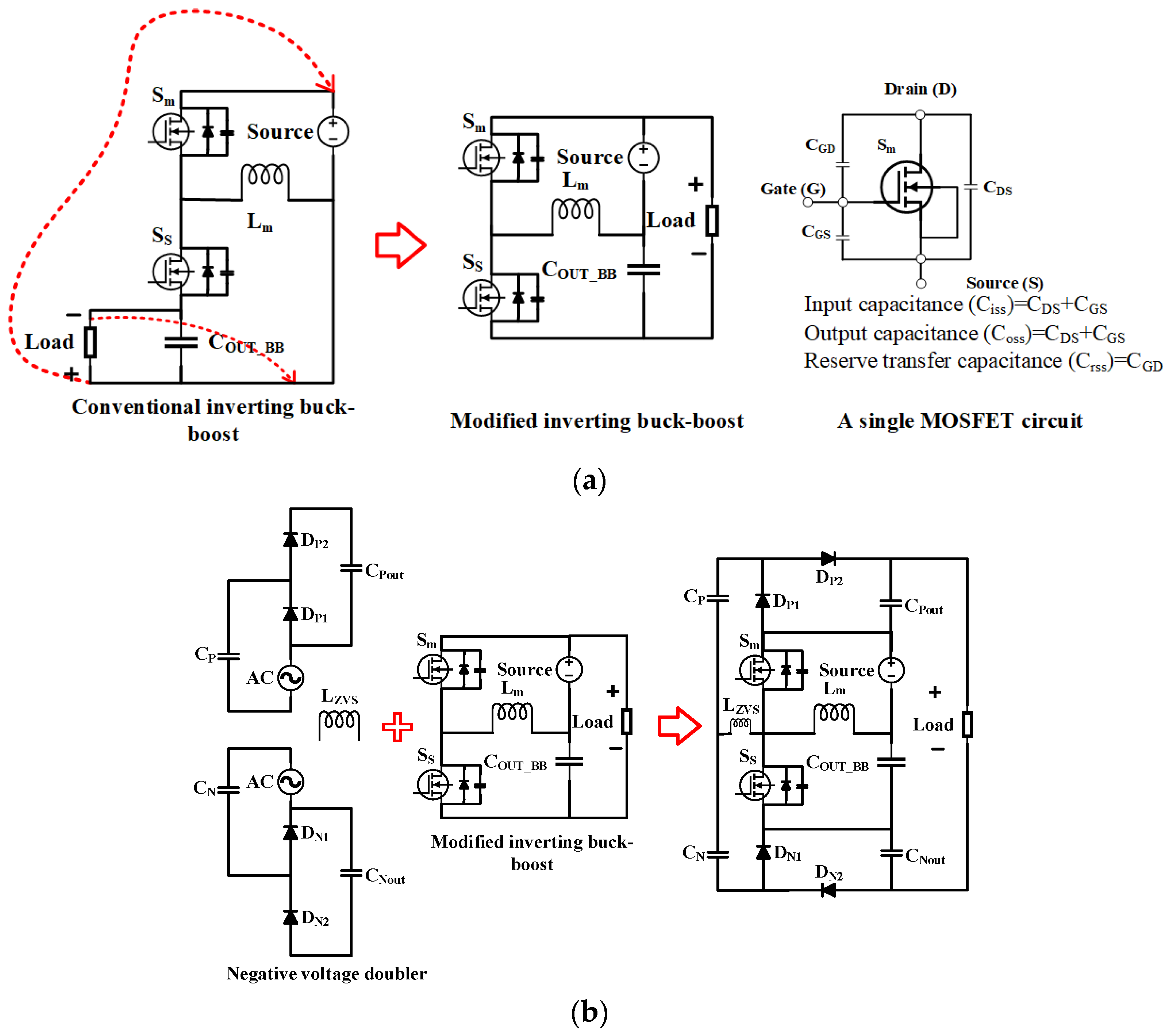
Figure 1. The revolution of the proposed topology; (a) The modified inverting buck-boost; (b) Integrating the voltage doublers.
Energies 17 01668 g001
Figure 2. The proposed topology N stages of the voltage doubler.
Energies 17 01668 g002
Figure 3. Operating waveform.
Energies 17 01668 g003
Figure 4. Operation Mode: (a) Mode 1; (b) Mode 2; (c) Mode 3; (d) Mode 4; (e) Mode 5; (f) Mode 6.
Energies 17 01668 g004aEnergies 17 01668 g004b
Figure 5. Prototype of the proposed converter.
Energies 17 01668 g005
Figure 6. Experimental voltage and current waveforms of the proposed converter: (a) Drain-Source voltage and current of the main switch Sm; (b) Voltage applied on the diodes DP2 and DN1 & Current flows through the diodes DP2 and DN1; (c) Voltage applied on the diodes DP1 and DN2 & Current flows through the diodes DP1 and DN2.
Energies 17 01668 g006aEnergies 17 01668 g006b
Figure 7. Capacitor voltage waveforms.
Energies 17 01668 g007
Figure 8. Measured waveforms of main inductor current ILm and ZVS inductor voltage VLZVS.
Energies 17 01668 g008
Figure 9. The measured efficiency curve of the proposed converter.
Energies 17 01668 g009
Figure 10. The measured efficiency curve of the proposed converter varies with input voltage.
Energies 17 01668 g010
Figure 11. Voltage gain graph [Sarikhani, A., 2020 [9], Lin, G., 2019 [12], Ismail, E.H., 2008 [25] (Figure 2e), Wu, G., 2015 [26] (Figure 4c), Jalilzadeh, T., 2023 [28], Marzang, V., 2019 [29], Kumar, A., 2020 [30], Prudente, M., 2008 [35] (Figure 38), Wu, B., 2016 [40], Yang, L., 2009 [46] (Figure 2c), AxeLZVSod, B., 2008 [47], Rosas-Caro, J.C., 2010 [48] (Figure 9)].
Energies 17 01668 g011
Figure 12. Maximum voltage stress on diodes graph [Sarikhani, A., 2020 [9], Lin, G., 2019 [12], Wu, G., 2015 [26], Kumar, A., 2020 [30], Prudente, M., 2008 [35], Wu, B., 2016 [40], Yang, L., 2009 [46]].
Energies 17 01668 g012
Figure 13. The proposed converter voltage gain with 1 stage, 2 stages, and 3 stages of VDs.
Energies 17 01668 g013
Figure 14. The output voltage comparison between theoretical and experiment.
Energies 17 01668 g014
Table 1. General specification of the proposed converter.
ParameterDesignatorValue
Input voltage V S o u r c e 40 V
Output voltage V O 380 V
Power P O 360 W
Switching frequency f S W 100 kHz
Table 2. Specification of component devices.
DevicesPart NumberSpecification
Switches ( S m , S S )SiR570DP150 V, 77.4 A
DiodesSTPS10200SF150 V, 10 A
Capacitors106MMR250K10 μF/150 V
Main Inductor ( L m )CTX100-10-52-R300 μH
ZVS Inductor ( L Z V S )XAL1580-302MED3 μH
Table 3. Comparison of the proposed converter with other existing topologies.
TopologyVoltage Gain (Vo/Vin)Voltage Stress on Switches (Vs/Vin)Maximum Voltage Stress on Diodes (VDmax/Vin)Maximum Voltage Stress on Output Capacitors (VCo/Vin)S/D/I/C/TEfficiency
[9] 2 D ( 1     D ) 2 S 1 : 1 D 1     D ,   S 2 : 1   +   D ( 1     D ) 2 1   +   D ( 1     D ) 2 NI2/3/2/3/1093.9%
[12] 3 1     D S 1 ,   S 2 : 1 1     D 2 1     D 3 1     D 2/2/2/3/995.3%
[25] (Figure 2e) 2 1     D 1 1     D NI 2 1     D 1/3/1/3/892.1%
[24] (Figure 4c) 2 1     D NI 2 1     D NI1/3/1/3/895.8%
[28] 2   +   D ( 1     D ) 2 S 1 : M C C M ( 1   +   1   +   12 M C C M ) 6 M C C M   +   1     1   +   12 M C C M S 2 : 2 M C C M 2 6 M C C M   +   1     1   +   12 M C C M 2 M C C M 2 6 M C C M   +   1 1   +   12 M C C M C o : 2   +   D ( 1     D ) 2 C 2 ,   C 3 : 2 M C C M 2 6 M C C M   +   1     1   +   12 M C C M 2/5/3/6/1695.22%
[29] 3   +   D 1     D 2 ( 1     D 1     D 2 ) M C C M   +   1 4 ,   M C C M     1 2 M C C M   +   1 2 3   +   D 1     D 2 ( 1     D 1     D 2 ) 3/3/2/3/1095.8%
[30] 3     3 D 1   +   D 2 1     3 D 1   +   D 2 3     3 D 1   +   D 2 1     3 D 1   +   D 2     1 2 3     3 D 1   +   D 2 1     3 D 1   +   D 2     1 3     3 D 1   +   D 2 1     3 D 1   +   D 2     1 2 2/6/2/4/1492.8%
[35] (Figure 38 with M = 1) 2 1     D 1 1     D 2 1     D 1 1     D 2/12/2/7/2395.3%
[40] (Figure 1h) 3     D 1     D 1 1     D 1 1     D 1 1     D 1/4/1/4/1095.44%
[46] (Figure 2c) 3     D 1     D 3     D 1     D     1 2 3     D 1     D     1 NI2/3/2/3/10NI
[47] (Figure 11) 2 D 1     D NINI 2 D 1     D 1/2/2/3/8NI
[48] (Figure 2, n = 2) N 1     D NI 1 1     D 1 1     D 1/5/1/5/1290%
[34] 3     D 1     D 1 1     D 1 1     D NI1/4/4/1/1096%
[39] (Figure 3) 4 1     D 1 1     D 1 1     D NI3/9/1/7/2097.35%
Proposed converter V o   =   3 1     D     4 L r C 1 Δ V o ( ( 1     D ) T S ) 2 4 L r C 1 Δ V o ( D T S ) 2 1 1     D 1 1     D     2 L r C 1 Δ V o ( ( 1     D ) T s ) 2     2 L r C 1 Δ V o ( D T s ) 2 1 1     D     2 L r C 1 Δ V o ( ( 1     D ) T s ) 2     2 L r C 1 Δ V o ( D T s ) 2 2/4/2/5/1397.4%
With S/D/I/C/T: Switch/Diode/Coupled Inductor/Single Inductor/Capacitor/Total, N: turns ratio of coupled inductor, NI: No information.
Disclaimer/Publisher’s Note: The statements, opinions and data contained in all publications are solely those of the individual author(s) and contributor(s) and not of MDPI and/or the editor(s). MDPI and/or the editor(s) disclaim responsibility for any injury to people or property resulting from any ideas, methods, instructions or products referred to in the content.