1. Introduction
The solid-state transformer (SST), which is also called a power electronic transformer (PET), is a new power electronic equipment that uses power electronic technology and high-frequency transformers [
1,
2,
3]. Although traditional line-frequency (LF) transformers have the advantages of a simple and reliable structure, as well as low maintenance costs, compared to SSTs, their disadvantages are also apparent. For example, they have a large weight and volume, poor controllability, and limited flexibility [
4,
5,
6]. In order to overcome these shortcomings, solid-state transformers with advantages of voltage regulation, energy management, higher power density, better controllability, and improved flexibility have gradually entered the vision of the public and have attracted more and more attention. SSTs have rapidly developed into substitutes for traditional LF transformers and are widely applied in smart distribution power grids, electric traction, and many other fields [
7,
8,
9].
In order to improve the performance of conversion efficiency, power density, controllability, flexibility, reliability, and manufacturing cost, various SST topologies have been presented and studied [
10,
11,
12,
13]. Generally, SST topologies are roughly classified into direct AC-AC topologies and indirect AC-DC-DC-AC topologies. Among the above two categories, AC-DC-DC-AC three-stage SSTs, which have the characteristics of reliable controllability and multiple functions for AC/DC outputs port, have been widely researched and applied [
14]. However, the multi-stage power conversion topologies lead to the significant disadvantage of relatively low conversion efficiency. In addition, bulky energy storage elements on the DC links unavoidably limit the power density of SSTs, and the electrolytic capacitors on the DC links lead to a short service life, reduced power density, and unstable reliability of the system if the correct design scheme and effective heat management are not adopted [
15]. The short lifespan of electrolytic capacitors is attributed to several factors. Firstly, the electrolyte inside the capacitor is prone to evaporation and drying, leading to a decrease in performance. Secondly, chemical reactions can occur within the electrolyte, further degrading the capacitor’s performance. Additionally, polarization effects and high temperatures accelerate aging, collectively contributing to the capacitor’s relatively short lifespan. Therefore, the direct AC-AC SST topologies, known as matrix-type SSTs, become a highly attractive alternative. Matrix-type SSTs contain relatively few power conversion stages, and there are no energy storage elements in the DC link, which makes it possible to use film capacitors instead of electrolytic capacitors [
16]. As a result, matrix-type SSTs provide the advantages of achieving improved power density, higher conversion efficiency, and better reliability [
17].
The two soft-switching isolation topologies frequently used in SSTs are the dual active bridge (DAB) and LLC resonant converter. Although the DAB converter has the ability to achieve higher conversion efficiency through good ZVS capability, as well as a reduced root-mean-square (RMS) and reactive power, the load and voltage-dependent ZVS characteristics make it unsuitable for direct AC-AC conversion applications [
18]. In [
19], a single-stage AC-AC SST-adopted series resonant converter (SRC) is presented, and it achieves the goal of higher efficiency. In [
20], a single-stage matrix-type SST based on a current-fed SRC is proposed, achieving zero voltage switching of the primary side switches over a relatively wide range of input voltage. However, the ZVS operation of the LV side, controllability of the output, and bidirectional power flow are not realized, as the LV side bridge is treated solely as an uncontrolled diode rectifier. In [
21], an AC-AC converter using an LLC resonant converter operated near the resonant frequency is developed, and the primary side switches of the transformer, which works at high frequency, are employed in the soft switching of the ZVS type.
Unlike the conventional single-phase SSTs, this paper presents a single-phase matrix-type AC-AC SST in order to overcome the main disadvantages of the bulky energy storage elements and inherent ripple power with double-grid frequency [
22]. The proposed SST has no energy storage elements in the DC link and adopts the LLC resonant converter, which is composed of a half-bridge on primary and secondary sides. Considering its natural voltage reduction capability of 2:1, the half-bridge structure is chosen, which helps to reduce the design difficulty of the transformer working at high frequency [
23]. At the same time, the number of switching devices and drivers is reduced, corresponding to a reduction in cost and an increase in power density.
The rest of the parts of this article are organized as follows.
Section 2 introduces the topology of the proposed matrix-type AC-AC SST in detail and analyzes the operating principles. Then,
Section 3 presents the analysis of ZVS and the control schemes. Afterward,
Section 4 shows the experimental results to verify the proposed methods and topologies. Finally, the conclusion of this paper is drawn in
Section 5.
2. Topology and Operating Principles of the Proposed SST
2.1. Proposed Topology
The topology, as illustrated in
Figure 1, comprises a full-bridge rectifier combined with a high-frequency (HF) half-bridge on the grid side, a half-bridge LLC resonant converter on the transformer’s secondary side, a buck converter on the DC-link side, and a full-bridge inverter on the load side.
Because the LLC operates in discontinuous conduction mode, the intermediate high-frequency stage in this topology is a half-bridge discontinuous conduction mode series resonant converter (HC-DCM-SRC). S1 to S4 and S11 to S14 operate at line frequency, while S5 to S10 operates at high frequency (HF). The buck circuit works in the CCM mode. In comparison to the traditional matrix-type SST, this topology reduces the number of HF switches, resulting in a considerably simplified converter structure and reduced hardware costs.
Cp1, Cp2, Cs1, Cs2, and Cb are film capacitors known for their extended lifespan and compact size. Consequently, the potential power density and reliability of the system can be improved. Lp serves as the input-filtering inductor. Cr is the resonant capacitor and Lr and Lm are the resonant inductor and magnetizing inductor, respectively. T represents the HF transformer, with a turns ratio expressed as 1: n.
Due to the matrix-type structure, the DC-link voltages are the absolute value of the sinusoidal voltage, eliminating the need for large electrolytic capacitors in the topology. Hence, the electrolytic capacitorless structure enhances the potential reliability and power density of the system and achieves transient energy balance between the source and load, avoiding ripple power with double-grid frequency.
2.2. Operating Principles
Given the similarity in operational principles between forward and reverse power transmission in the SST, this section uses forward power transmission as an example.
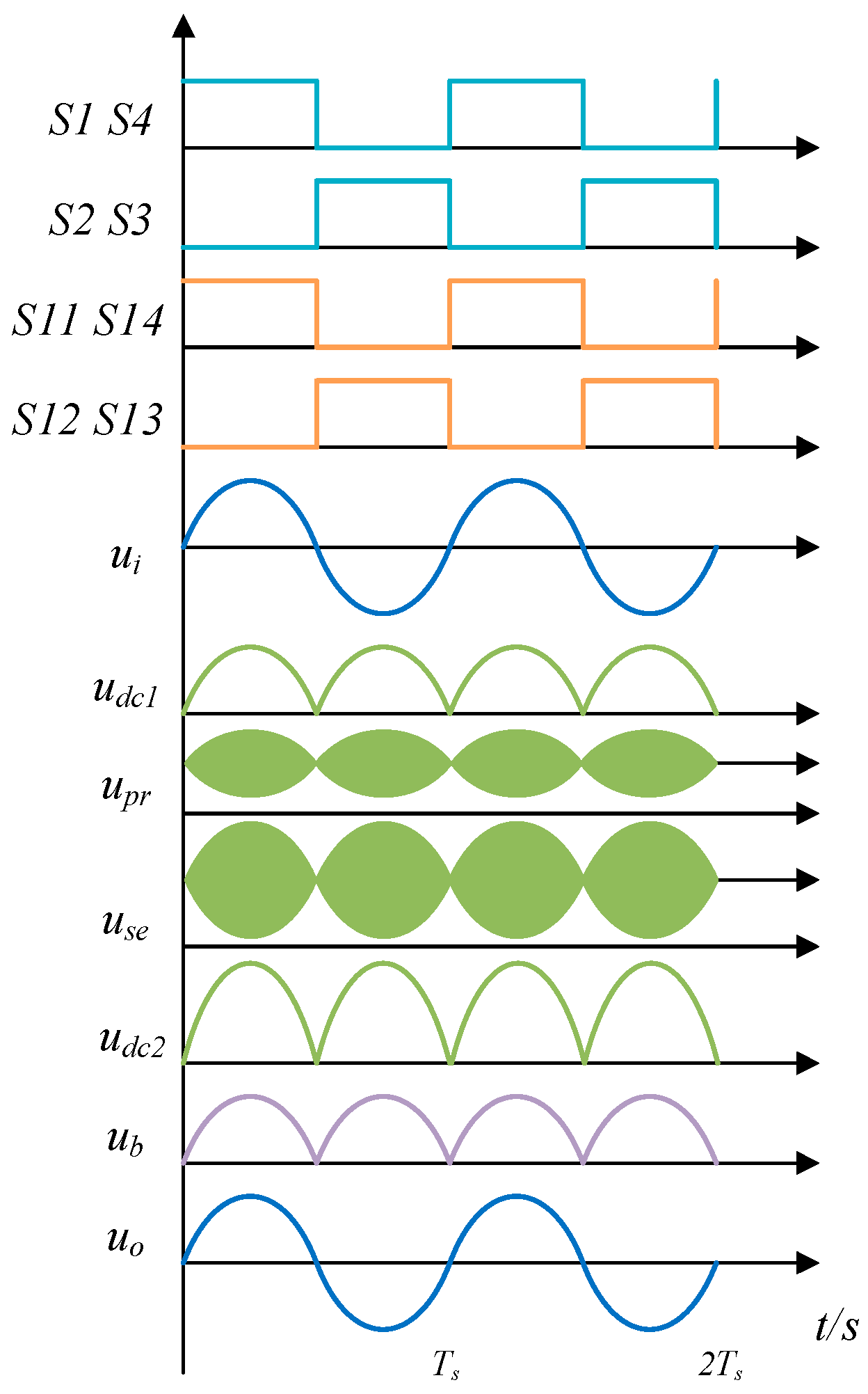
The operation waveforms of the SST are displayed in
Figure 2, with
S1 to
S14 representing the gate signals. As depicted in
Figure 2 the full bridges on the grid and load sides commutate with LF in accordance with the polarity of the input voltage
ui(
t). When
ui(
t) > 0, switches
S1,
S4,
S11, and
S14 are turned on, while switches
S2,
S3,
S12, and
S13 are turned off. Conversely, when
ui(
t) < 0, the switching modes are reversed. Consequently, the DC-link voltages
udc1(
t) and
udc2(
t) are the absolute value of the sinusoidal voltage. To facilitate subsequent analysis, this article assumes that
ui(
t) =
uo(
t). Hence,
From (1), it can be seen that the topology achieves transient energy balance between the source and load, hence avoiding ripple power with double-grid frequency and providing inherent power factor correction (PFC).
The resonant frequency
fr is determined by the resonant inductor
Lr and resonant capacitor
Cr, and the expression is as follows:
When the transformer’s magnetizing inductance
Lm is added, the resonant frequency
fm is expressed as follows:
According to the relationship between fr, fm, and fs, there are three types of operating states of the LLC resonant circuit. When the switching frequency fs > fr, the primary side switches can achieve soft switching, but the secondary side diodes work in continuous conduction mode (CCM) and cannot achieve soft switching. When fr > fs > fm, switches on both primary and secondary sides can achieve soft switching. When fm > fs, the primary side switches operate in the capacitive domain and keep hard switching, which means that the switching loss is large. Therefore, in this paper, to achieve soft switching for both primary and secondary side switches of the LLC converter, the switching frequency fs is set to be lower than the resonant frequency fr.
For the buck converter, in order to regulate voltage and meet the load requirements,
S9 and
S10 are operated at high frequency to offer the desired amplitude of the half-cycle sinusoidal voltage
ub(
t).
S9 and
S10 complementally conduct, with the duty cycle of
S9 being
Dα. According to the volt-second balance principle, the output voltage of the buck circuit is
For the full-bridge inverter on the output load side, the switches S11~S14 are commutated with line-frequency and have the same operating principles as the switches S1~S4. When the instantaneous value of the input voltage ui(t) turns to positive, switches S11~S14 are turned ON, while correspondingly switches S12 and S13 are turned OFF. On the contrary, When the instantaneous value of the input voltage ui(t) turns to negative, switches S11~S14 all act in reverse. Then, the half-cycle sinusoidal voltage ub(t) is turned to the expected sinusoidal output voltage uo(t).
In short, the designed topology of the single-phase matrix-type AC-AC SST using the appropriate operating principles gets rid of bulky energy storage elements, obtains the sinusoidal input and output, and avoids the ripple power with double-grid frequency.
Figure 2 represents some key waveforms of the proposed SST.
3. ZVS Analysis and Control Scheme of the Proposed SST
3.1. ZVS Analysis
Usually, the high conversion efficiency is considered as one of the most important factors in the design of SST. Reducing switching loss and conduction loss can improve conversion efficiency. Therefore, the proposed SST needs to achieve ZVS on both the primary and secondary sides of the LLC SRC as much as possible.
Unlike the modulation strategy of a traditional LLC SRC, the proposed matrix-type SST topology adopts a novel control method to achieve ZVS operation of the secondary side. This is accomplished by generating a small spike in the secondary-side resonant current through introducing a slight phase shift between the gate control signals of the primary and secondary sides. Consequently, the current spike is utilized to discharge the effective output capacitor of the secondary-side MOSFET, thereby achieving ZVS. The specific waveform of the novel control method mentioned above is represented in
Figure 3, where
Tdp refers to the dead time of the bridge arm on the primary side,
Tds refers to the dead time of the bridge arm on the secondary side, and
Tp refers to the phase shift between the gate signal on the primary side and the secondary side;
up refers to the primary bridge voltage of the LLC resonant converter, and
us refers to the secondary bridge voltage of the LLC resonant converter.
As shown in
Figure 3, near the dead time, the gate signals of the primary and secondary bridge arms of the LLC resonant converter are not exactly the same; a tiny phase shift
Tp exists. As a result, a small voltage-second product is generated due to the tiny phase shift
Tp during this interval. This product is then added to the resonant inductor
Lr on the primary side, thereby creating a small resonant current spike on both the primary and secondary sides of the high-frequency transformer. Due to the generated negative resonant current spike in the secondary side of the high-frequency transformer, the parasitic capacitance of the switches on the secondary side is turned on and discharged, which finally realizes the soft switching of ZVS for all switches on the secondary side. As for the switches on the primary side, when designing this SST, the magnetizing inductance of the transformer is selected to be small enough to ensure that there is a large enough magnetizing current so that the parasitic capacitance of the switches on the primary side bridge arm can be turned to on and discharged within the dead time, which ensures the soft switching of ZVS for all switches on the primary side.
The design parameters to be considered for soft switching include switching frequency, magnetizing inductance, and dead time; then, the appropriate phase shift can be calculated. In short, the proposed control method can realize the soft switching of ZVS for all switches of the LLC resonant converter.
3.2. Control Scheme
The full-bridge rectifier on the input grid side and the full-bridge inverter on the output load side both operate in the line-frequency commutated, and the control method of the unfolding bridge is relatively simple. Therefore, in this section, the analysis of the control scheme should focus on the buck converter providing a voltage regulation function. The detailed explanation is displayed as follows.
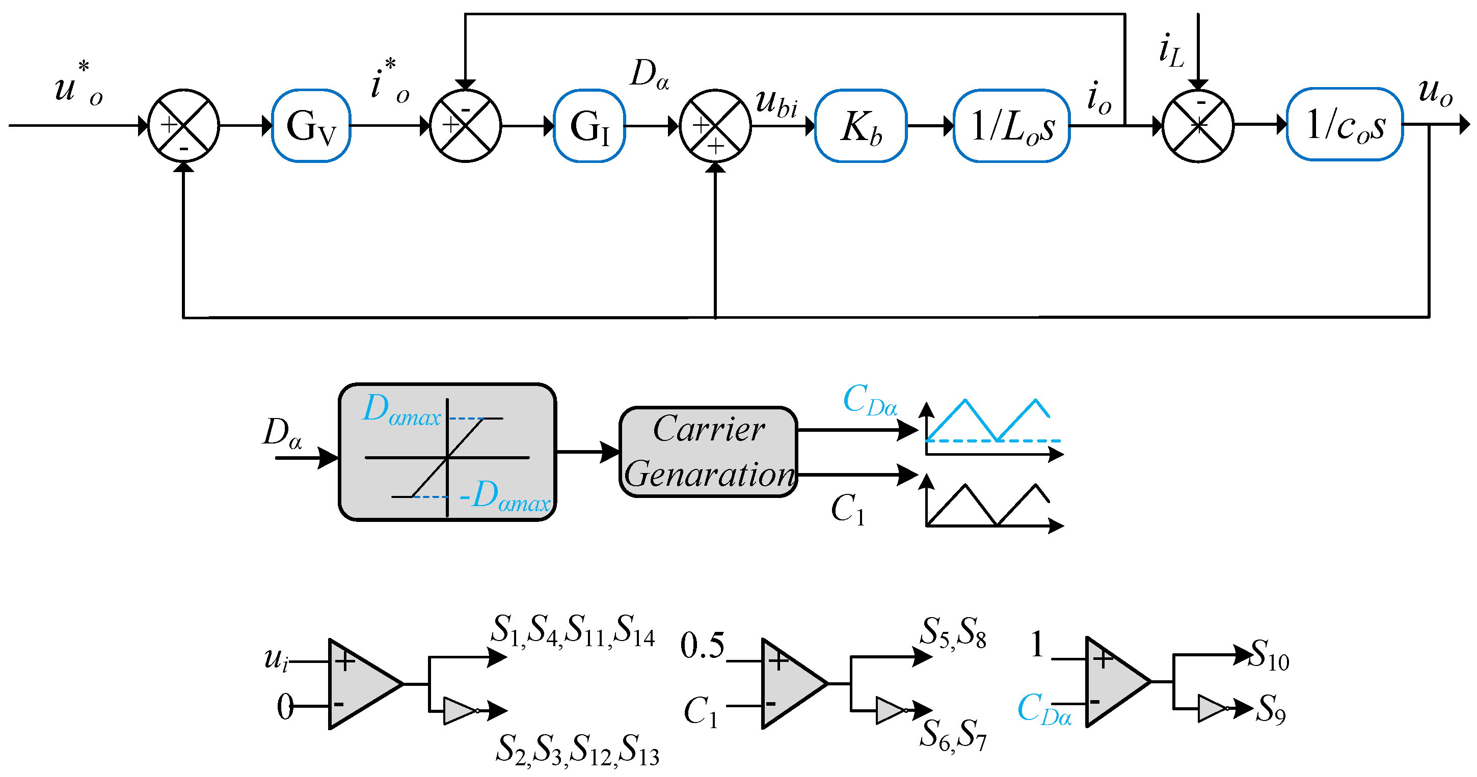
The primary objective of designing a closed-loop system is to attain the desired output waveform while enhancing resilience to disturbances. This ensures that, even during transient load variations or input voltage disturbances, the output voltage amplitude remains constant, so it plays an important role in the stability of the system. The voltage and current double-closed-loop control structure obtains the reference current of the current inner loop from the voltage outer loop controlled by feedback. The control scheme of the voltage and current double-closed-loop control system is represented in
Figure 4, where
u*
o refers to the desired output voltage of the inverter,
i*
o refers to the reference current of the output inductor,
iL refers to the current of the load,
ubi refers to the modulation voltage, and
kb refers to the equivalent gain of the buck converter. The regulator
GI(
s) used by the current loop is the PI regulator, and the expression of
GI(
s) is as follows.
The regulator
GV(
s) used in the voltage outer loop is also the PI regulator, and the expression of
GV(
s) is as follows:
Different from the half-sinusoidal voltage shape of the secondary-side DC-link, the initial modulation voltage must be normalized according to the value of the instantaneous DC-link voltage on the secondary side.
4. Experimental Results
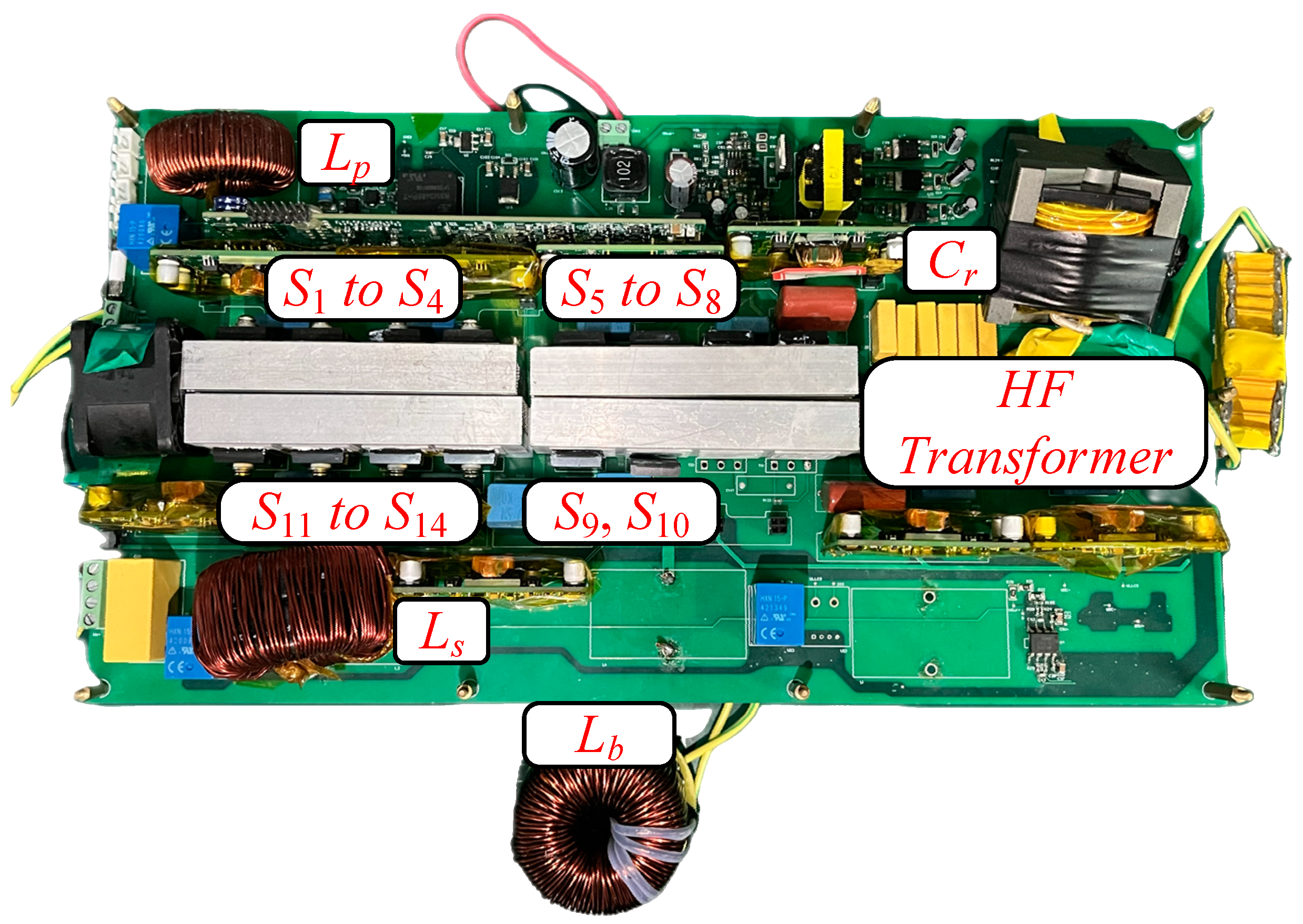
In this section, a 1 kW SST prototype is developed and tested to validate the feasibility and functionality of the proposed methods. The prototype of the proposed SST is shown in
Figure 5, and the system experimental parameters are given in
Table 1.
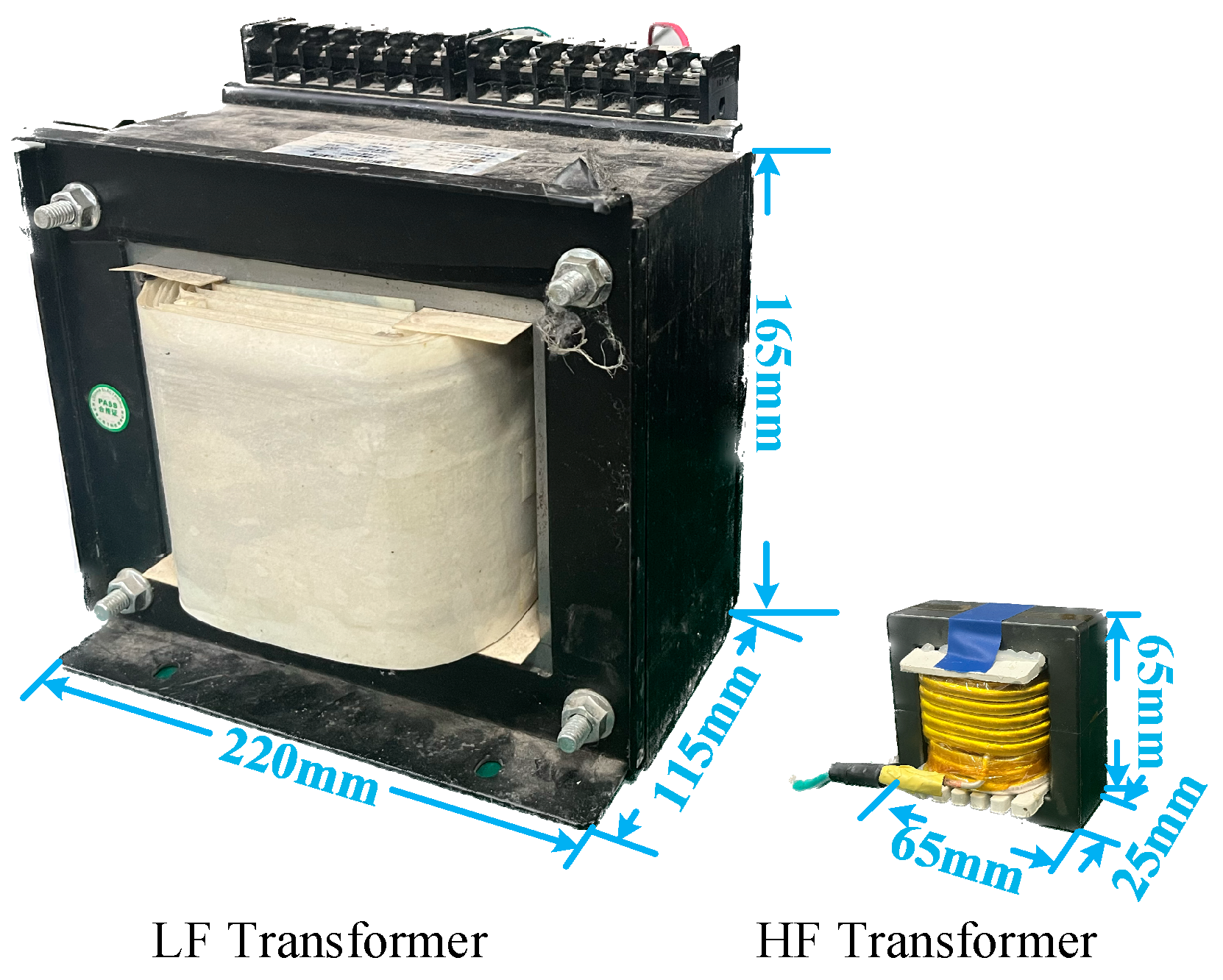
Figure 6 illustrates a comparison between the high-frequency SST proposed in this paper and traditional line-frequency transformers, with relevant parameters summarized in
Table 2. As depicted in the figure, under the same power transmission conditions, the power electronic transformer exhibits significant advantages in terms of volume and weight compared to traditional line-frequency transformers. Therefore, the SST is highly suitable for applications where weight and volume constraints exist, and there are high demands for power density.
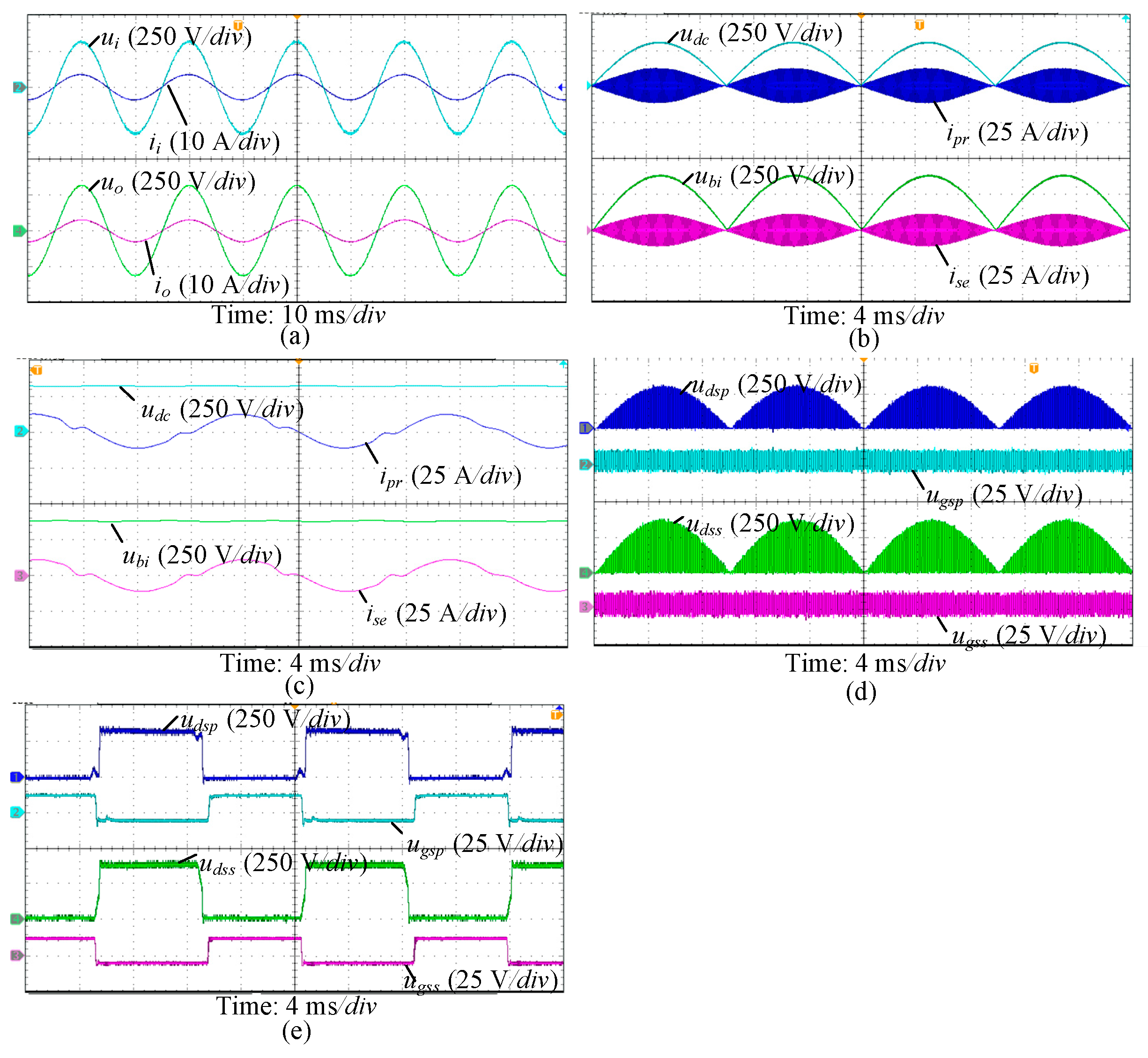
Figure 7 depicts the key waveforms of the proposed SST working under the original condition.
Figure 7a displays the input and output voltage as well as current waveforms of the converter under rated voltage (1 kW condition). It can be observed from the figure that both the input and output voltages are 220 V. The input current is sinusoidal and in phase with the input voltage. Additionally, the output voltage is also sinusoidal and closely tracks the reference. Thus, it is evident that the proposed PET can generate sinusoidal input current and controllable output voltage. In
Figure 7b, it becomes evident that the matrix-type structure of this SST results in the DC-link voltage being equal to the absolute value of the input voltage, that is,
udc(
t)= |
ui(
t)|. This design effectively eliminates the issue of dual LF power pulsation induced by traditional HF modulation. Additionally, it enables the substitution of electrolytic capacitors with thin film capacitors, leading to a substantial increase in the system’s power density. The transformer switching frequency is 65 kHz, and the current waveforms at the input and output terminals of the transformer both exhibit a sinusoidal envelope. In
Figure 7e,
udsp,
ugsp,
udss, and
ugss are the primary-side drain-to-source voltage and gate-to-source voltage, and the secondary-side drain-to-source voltage and gate-to-source voltage, respectively. It can be observed in
Figure 7e that, for both sides of MOSFETs, the rising edge of the gate-to-source voltage lags behind the falling edge of the drain-to-source voltage, demonstrating the ZVS operation of the SST.
The key waveforms of the proposed SST working under the light-load condition are given in
Figure 8. The output power is 500 W, which is half of the rated power. The key waveforms of the proposed SST working under the heavy-load condition are given in
Figure 9. The output power is 1200 W. The input voltage of the two groups mentioned above is the same as the original condition. Experimental results prove that the proposed SST obtains the desired output and achieves ZVS under different load conditions.
Figure 10 shows the key waveforms of the proposed SST working with higher input voltage. The input voltage is selected to increase by 15% from 220 to 253 Vrms.
Figure 11 shows the key waveforms of the proposed SST working with lower input voltage. The input voltage is selected to decrease by 5% from 220 to 209 Vrms. The output power of the two groups is equal to the rated power. The implementation results indicate that the voltage control method proposed in this paper can effectively maintain the output voltage constant when the input voltage changes..
As can be seen from the above experimental results, the proposed SST in this paper realizes the main purpose of sinusoidal input and output and ZVS operation on both the primary and secondary sides with wide input voltage and output load ranges.
The proposed SM-SST is compared with the other converters presented in the literature, and the results are presented in
Table 3.
The system efficiency is measured using the HIOKI 3390 power analyzer, which is manufactured by HIOKI Corporation from Japan. As depicted in
Figure 12,at the rated load condition, the peak efficiency reaches 95.2%. The proposed topology in this paper significantly improves transmission efficiency.
Compared to [
24,
25], the proposed SST achieves ZVS for all high-frequency switches, even when the DC-link voltage varies. In contrast, refs. [
24,
25] always have two to four switches unable to achieve soft switching within half of the low-frequency cycle, resulting in significant switch losses. Unlike [
25], the proposed topology in this paper adopts a matrix structure, allowing for the use of small film capacitors instead of electrolytic capacitors. This improvement enhances system stability and compactness. Compared to the literature [
19], the SST proposed in this paper reduces the use of switches and inductors, thereby reducing switch conduction losses and hardware costs. Although the topology in this paper adopts a half-bridge structure on the primary side, resulting in a doubling of the effective current, the proper selection of switch devices allows this topology to achieve higher power density with fewer components, a smaller size, and a lower system cost.
5. Conclusions
This paper presents a single-phase matrix-type AC-AC SST designed to eliminate ripple power with double-grid frequency. By sharing the filter capacitor between the HF half-bridge and the LF rectifier on the primary side, significant reductions in power switches and conducting losses can be achieved. Additionally, through proper analysis of soft switching characteristics, all HF switches can realize ZVS under time-varying DC-link voltage, further reducing switching losses. Moreover, the matrix-type topology eliminates ripple power with double-grid frequency, and the use of film capacitors enhances system reliability and lifespan. The control strategy, employing a buck converter for power and AC output regulation, is simple and reliable, achieving PFC without the need for a current loop. Because the SST proposed in this paper enables direct AC-AC conversion and features a compact structure with high efficiency, future work will primarily focus on applying this converter to low-voltage distribution networks where the input and output voltage frequencies are the same, or in applications such as aerospace, aviation, transportation, and other scenarios with strict requirements on volume and weight.

