Article

Quantitative Analysis of Balancing Range for Single-Phase 3L-NPC Converters

College of Electrical Engineering, Sichuan University, Chengdu 610065, China
*
Author to whom correspondence should be addressed.
Energies 2024, 17(6), 1464; https://doi.org/10.3390/en17061464
Submission received: 19 February 2024 / Revised: 14 March 2024 / Accepted: 15 March 2024 / Published: 19 March 2024
(This article belongs to the Section F3: Power Electronics)

Abstract

:
Multiple techniques have been suggested to achieve control balance in single-phase three-level neutral-point clamped (3L-NPC) converters. Nevertheless, there is a deficiency of quantitative calculations related to the extent of balancing. Operating beyond the balancing range may result in a sequence of safety incidents. This paper presents a conceptualization of the 3L-NPC converter as two cascaded H-bridges. By employing power conservation principles, the balancing range for the NPC converter is derived, and two novel methods are investigated to broaden the balance range in accordance with the calculated balance range. A comparison is made among the balancing ranges under different balancing control methods. This study establishes a theoretical foundation to ensure the secure and stable operation of the NPC converter.

1. Introduction

Carbon dioxide (CO2) emissions have substantial environmental consequences, as they contribute to climate change and global warming. Multilevel converters are increasingly crucial in mitigating CO2 emissions in sectors such as automotive [1,2] and electrical power [3]. In 2021, transportation and electric power sectors in the United States were responsible for 38% and 33% of energy-related emissions, respectively [4]. The combustion of conventional petroleum fuels in automotive internal combustion engines generates CO2. Moreover, compared to traditional gasoline vehicles, electrified vehicles, like hybrid electric vehicles (HEVs), plug-in hybrid electric vehicles (PHEVs), and electric vehicles (EVs), markedly reduce fuel consumption, leading to a significant decrease in tailpipe CO2 emissions [5]. Power electronics is increasingly vital in electrified vehicle applications, offering compact and highly efficient solutions for power conversion tasks, such as motor control and conversion between high-voltage and low-voltage batteries [6]. Similarly, the electric power sector is adopting renewable energy systems to reduce reliance on fossil fuels for electricity generation [7], with power electronic converters commonly employed in wind energy and photovoltaic (PV) systems [8].
The 3L-NPC converter, as a type of multilevel converter, is widely applied in various industrial sectors, including high-speed railway traction [9,10], photovoltaic systems [11,12], and power factor correction [13]. However, the imbalance in the voltage of the dc capacitors poses operational challenges for the converter. This imbalance arises from factors like variations in circuit component characteristics and non-ideal properties of switching devices [14]. The uneven voltages across the capacitors result in distortion in the waveforms of the ac voltage and current and also increase the risk of over-voltage damage to the switching devices and clamping diodes [15,16,17,18,19]. Therefore, it becomes imperative to ensure equal voltages across the dc link capacitors and expand the balance range of the topology.
Currently, various methods have been proposed and proven effective for balancing the dc voltage in single-phase 3L-NPC converters. These methods can be classified into hardware approaches utilizing auxiliary balancing circuits [16] and modulation methods employing redundant switching states [20,21,22,23,24,25,26,27,28,29,30,31,32,33]. In reference [16], a passive RLC circuit connected in parallel to the load is introduced, allowing additional current flow. A coordinated modulation strategy was developed to generate harmonics at half the switching frequency in the ac voltage and dc link capacitor currents. Modulation methods have garnered more research attention due to their advantage without adding extra devices. Redundant switching states produce the same output voltage level but have different effects on the charge and discharge of the two dc link capacitors. Some researchers modify the duration of the redundant states [20,21,23,24,27,28,30,33] while others select one redundant state from a pair based on the polarity of voltage and current variables [22,25,26,29,31,32,33]. Both of these strategies are intended to reassign the charging and discharging times of the two capacitors, thereby altering the voltages across the two capacitors.
However, when the load imbalance increases significantly, or under extreme operating conditions, these balancing control methods may fail to maintain the desired voltage balance. Thus, it is essential to derive the balancing ranges under different balancing control methods. Nevertheless, quantitative calculations to determine the balance range of the single-phase 3L-NPC converter are currently lacking.
Several studies have examined the balance range of other multilevel converters. In reference [34], the balance range for the four-level diode-clamped converter is proposed based on a parameter related to midpoint currents. Yet, this method is unsuitable for sinusoidal pulse width modulation and entails complex mathematical calculations. The balance range for the three-phase 3L-NPC converter is presented in the form of a power ratio in reference [35], but the method for calculating the maximum injected dc voltage bias is restricted to an additional balance circuit. Reference [36] addresses the balance range through a vector diagram for the two-cell cascaded H-bridge rectifier. Nonetheless, this method does not elaborate on the extension of the balance range. Each redundant switch state affects the voltages of both capacitors simultaneously, making it challenging to establish a direct relationship between individual capacitor voltages and modulation signals, thus complicating the computation process. Therefore, there is a need for analysis to determine the balance range of these balance control techniques in the single-phase 3L-NPC converter.
In addition to the aforementioned studies, there have been investigations into various application scenarios of the single-phase 3L-NPC converter, with a focus on different equivalent loads and specific balance issues. Some researchers have utilized a single equivalent dc load and primarily examined the initial voltage imbalance between capacitors [20,21,22,25,26,30]. To simulate asymmetry in the capacitance parameters, a few researchers have introduced an additional resistance in parallel with one of the dc link capacitors [23]. Others have studied the imbalance in capacitor voltages during inverter operation [24,27,29,31,32,33]. A two-equivalent-load topology that represents a typical traction drive unit in high-speed railway trains is investigated in reference [28]. In this topology, the single-phase 3L-NPC converter is connected to an inverter–motor system comprising a three-phase 3L-NPC inverter and four traction motors [28]. The two-equivalent-load topology in [28] experiences the most significant pressure in terms of dc voltage imbalance and is also used to validate the effectiveness and robustness of the proposed voltage balancing technique in [20]. Therefore, the two unbalanced equivalent loads are also adopted by this article for analysis.
The main contribution of this article lies in the conceptualization of the single-phase 3L-NPC converter as a two-unit cascaded H-bridge system. By applying the principle of power conservation, this study introduces the concept of the balance range for the single-phase 3L-NPC converter, investigates two novel approaches to expand the balance range, and performs a comparative analysis of this range using various balancing control methods. These findings establish a theoretical foundation for ensuring the secure and stable operation of single-phase 3L-NPC converters.
The rest of this article is organized as follows. In Section 2, the operational principles and the criteria for design balancing methods of the single-phase 3L-NPC converter are provided. In Section 3, the voltage balancing range is calculated. In Section 4, the balancing capabilities of two typical methods are clarified and two novel methods are explored to extend the balance range. The balancing abilities of these methods are compared in Section 5. In Section 6, the effectiveness of the proposed methods is verified through simulation results, followed by a conclusion in Section 7.

2. System Description

In this section, a brief description of the operational principles of the single-phase 3L-NPC converter is provided. The reasons behind DC voltage imbalance are explored and the criteria used for designing balancing methods are analyzed.

2.1. Operational Principles

The simplified topology of the single-phase 3L-NPC converter is shown in Figure 1, which consists of two legs, “Leg a” (Sa1, Sa2, Sa3, Sa4) and “Leg b” (Sb1, Sb2, Sb3, Sb4). us, uab, and udc represent the ac source voltage, the voltage of the converter on the ac side, and the total dc voltage, respectively. L represents the equivalent inductance on the ac side, while the ac side equivalent resistance is neglected [28]. is is the ac current. ip, in, io, and ir are the currents on the dc side. The resistors R1 and R2 are equivalent loads. u1 and u2 are the voltages of the dc link capacitors C1 and C2, respectively. The LC filter is responsible for filtering out second-order harmonics in the dc voltages.
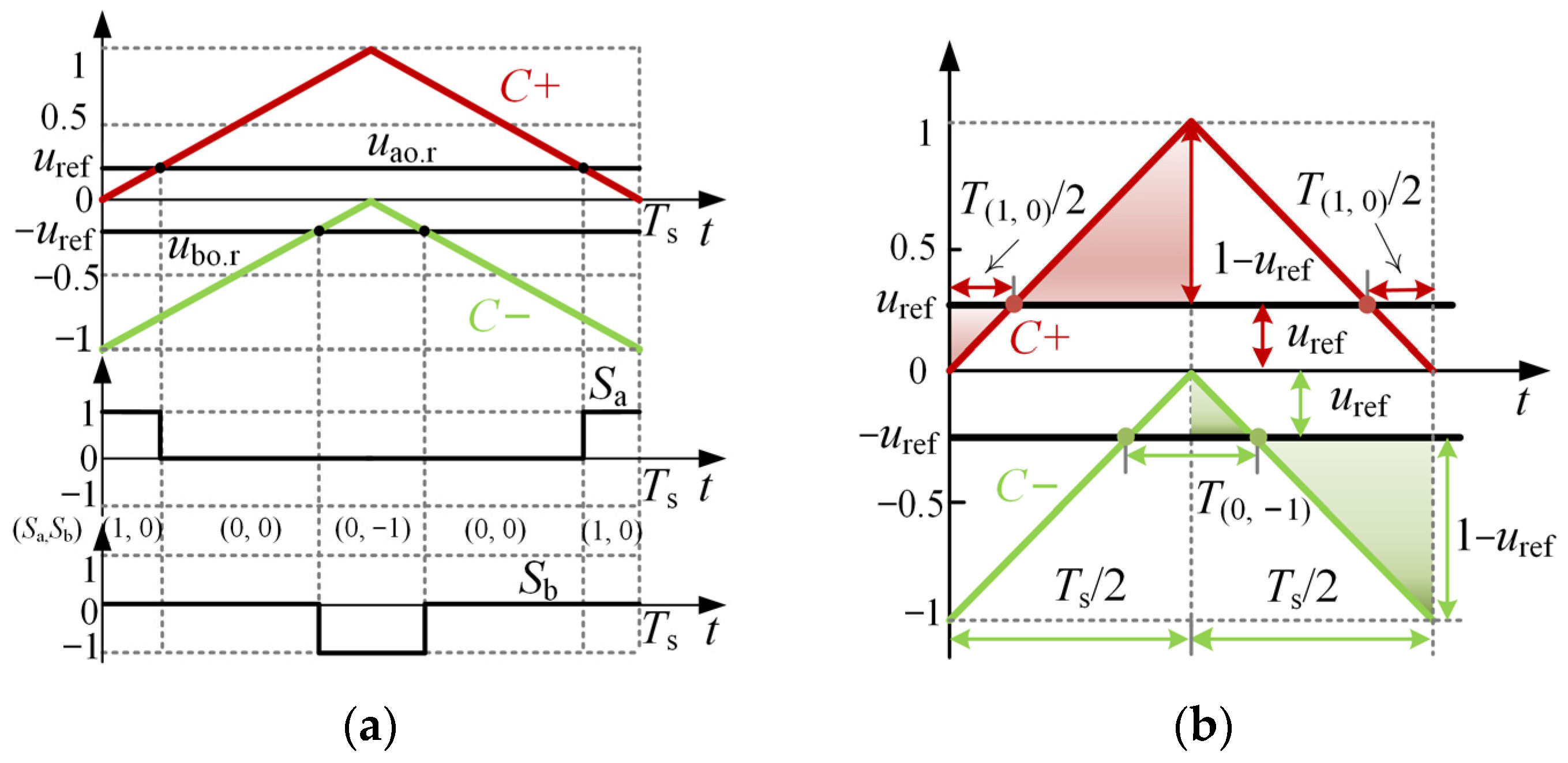
The conventional modulation strategy employed in 3L-NPC converters is illustrated in Figure 2. The switching functions (Sa and Sb) are produced by the comparison between the reference voltages of “Leg a” and “Leg b” (uao.r and ubo.r) and the triangle carriers (C+ and C−). The switching functions (Sa and Sb) for the two legs are determined based on the outcomes of comparisons, which can be expressed as follows:
S i ( i = a   or   b ) = 1 u io . r > C + 0 C u io . r C + 1 u io . r < C
where Ts is the cycle of the triangle carriers and also the switching cycle.
When the switching function Si (i = a or b) is 1, the switches Si1 and Si2 are activated; when Si (i = a or b) equals 0, the switches Si2 and Si3 are activated; when Si (i = a or b) equals to −1, the switches Si3 and Si4 are activated.
Reference voltages (uao.r and ubo.r) can be expressed as follows:
u ao . r = u ref u bo . r = u ref
where uref is the reference voltage of uab. And uref is between 0 and 1.
The frequency “fs” of triangle carriers is significantly higher than the fundamental frequency of the converter (f1). uao.r and ubo.r can, therefore, be treated as constant throughout each individual switching cycle “Ts”.
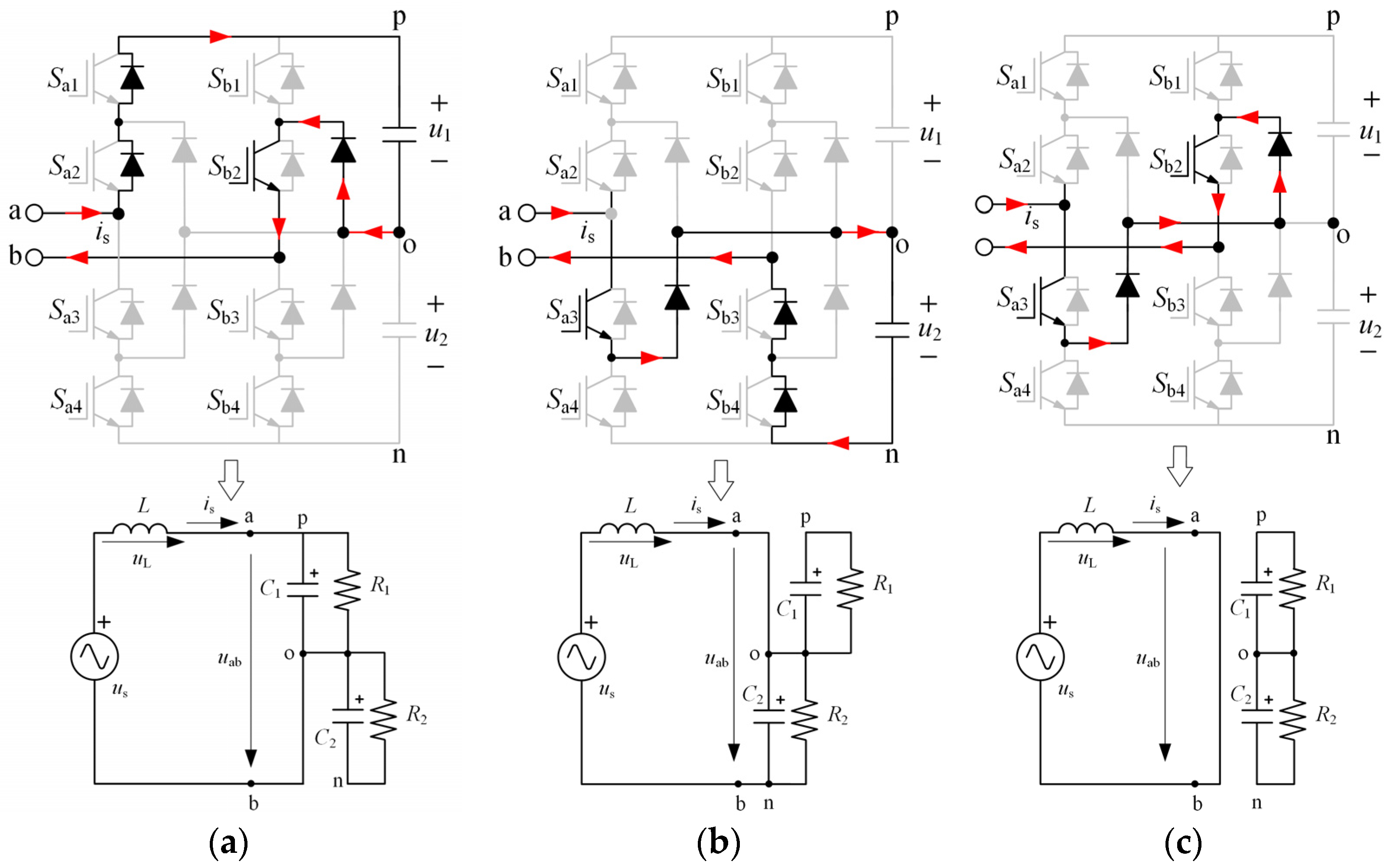
Based on the aforementioned modulation principles, when 0 ≤ uref ≤ 0.5, switching states (Sa, Sb) = (1, 0), (0, −1), and (0, 0) are involved in a Ts, as depicted in Figure 2a. When the ac current is flows from node a to node b, the equivalent circuits for the three states are shown in Figure 3. The gray elements are where is does not pass by. Sometimes, is flows through the diode connected in parallel with a switch, although the switch is activated. It depends on the direction of is, for the turn-on condition for IGBT requires the gate voltage to exceed the threshold voltage and the gate current to be sufficiently large, while maintaining the correct polarity. If is flows from node b to node a, the equivalent circuit can be figured out in a similar way.
As illustrated in Figure 2b, two similar triangles are utilized in the calculation of the switching states durations. The time intervals corresponding to (Sa, Sb) = (1, 0), (Sa, Sb) = (0, −1), and (Sa, Sb) = (0, 0) within a cycle are denoted as T(1, 0), T(0, −1), and T(0, 0), respectively. Similarly, the durations of other switching states can be obtained.

2.2. Mathematical Model

By utilizing Sa and Sb, the currents ip, in, and io can be expressed as [20]
i p = ( S a S b ) ( S a + S b + 1 ) 2 i s i n = ( S a S b ) ( S a + S b 1 ) 2 i s i o = i p + i n
Once the entire system reaches a steady state, the rate of the dc voltages across R1 and R2, (u1 and u2) becomes zero. Consequently, based on Kirchhoff’s current law (KCL), the average value of current ir within T1 is equal to the average of io, denoted as i ¯ o . By substituting the durations of switching states into (3), i ¯ o can be obtained as follows:
i ¯ o = 1 T 1 T 1 S a 2 S b 2 i s d t = 0
Based on Equation (4), the equivalent loads R1 and R2 operate in series and share the voltage. Therefore, the signs of (u2u1) and (R2R1) are identical, and this can be expressed as follows:
sgn ( u 2 u 1 ) = sgn ( R 2 R 1 )
where sgn(.) is a sign function. This “series voltage sharing” situation results in the imbalance of dc voltages on the two equivalent loads.
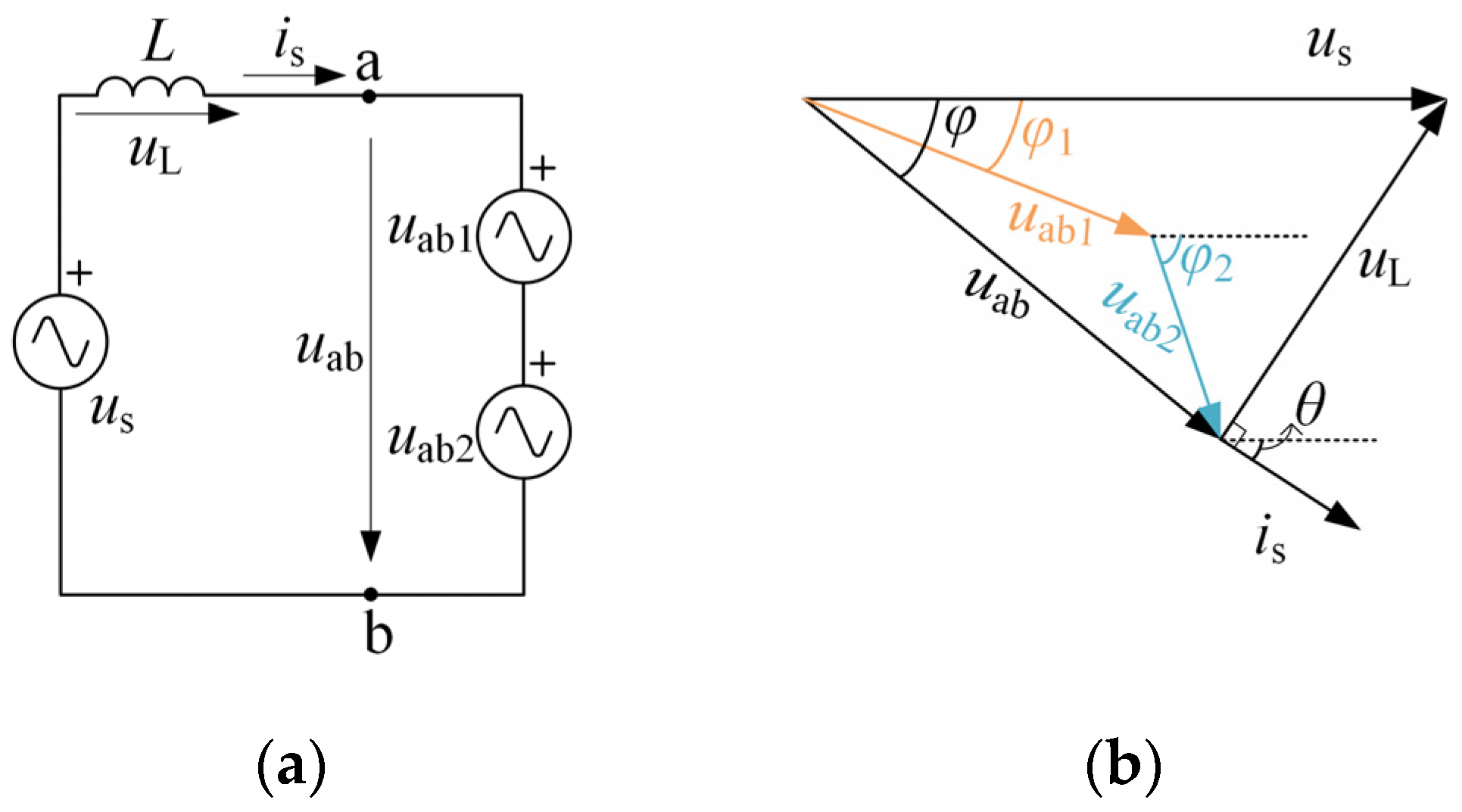
Figure 4a depicts the equivalent circuit of the system from the ac side, while Figure 4b presents the vector diagram of the ac voltages. The voltage across inductor L is denoted as uL. The equivalent voltage vectors of dc loads R1 and R2 are represented as uab1 and uab2, respectively. The phase offset between uab and us is denoted as φ, and θ represents the phase difference between is and us. The vectors in Figure 4b can be expressed as follows:
u s = U s cos ( ω 1 t ) u ab = S ab u dc = U ab cos ( ω 1 t φ ) i s = I s cos ( ω 1 t θ )
where Us, Uab, and Is are the magnitudes of us, uab, and is, respectively. ω1 is the fundamental angle frequency. Sab is the ideal switching function of the circuit. udc is the dc voltage.

2.3. Voltage Balancing

The following analysis is based on the ideal conditions.
The reference voltages and switching functions, u ao . r con , u bo . r con , S a con , and S b con , can be expressed in (7) during the voltage balancing process.
S a con u ao . r con = u ref + d z S b con u bo . r con = u ref + d z
where dz is the offset voltage.
Substituting (7) into (3), the currents ip and in can be expressed as
i p = u ref ( 2 d z + 1 ) i s i n = u ref ( 2 d z 1 ) i s
The current io can be described as
C d u 1 d t d u 2 d t + u 1 R 1 u 2 R 2 = i o
By applying io from (3) and (8) into (9), the offset voltage dz is given by the following equation:
d z = U dc * R 2 R 1 8 R 1 R 2 u ref i s sgn ( u ref i s ) sgn ( R 2 R 1 )
where U dc * represents the rated value of udc.
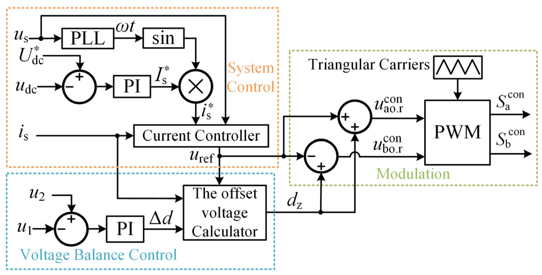
However, (10) is not applicable in cases where the unbalanced equivalent loads are unknown. To solve this problem, the voltage balance control is designed as illustrated in Figure 5. In this control scheme, the difference between u2 and u1, denoted as Δd, is processed by a PI regulator, and dz is calculated based on Δd. Since passing through a PI regulator does not alter the sign of a variable, Δd and (R2R1) share the same signs. Therefore, the sign of dz in (10) can be described as follows:
sgn ( d z ) = sgn ( u ref i s Δ d )
As depicted in Figure 5, the rectifier control strategy employed in this article utilizes a dual closed-loop PI control strategy. During the voltage balance control stage, various control methods can be introduced to enhance the range of voltage balancing based on Formula (11).

3. Quantitative Analysis of Voltage Balancing Range

In this section, the single-phase 3L-NPC converter can be represented as a two-unit H-bridge. Based on this configuration, the calculation of the maximum level of dc load imbalance and balance range are elaborated by the vector diagram.

3.1. The Two-Unit H-Bridge Equivalence

As depicted in Figure 1, the active power absorbed by the loads in a T1 can be expressed as follows:
P 1 = 1 T 1 0 T 1 u 1 i p d t = 1 T 1 0 T 1 ( 1 2 U dc * ) i p d t P 2 = 1 T 1 0 T 1 u 2 ( i n ) d t = 1 T 1 0 T 1 ( 1 2 U dc * ) ( i n ) d t
where P1 and P2 are the active powers absorbed in a fundamental cycle “T1” by R1 and R2, respectively.
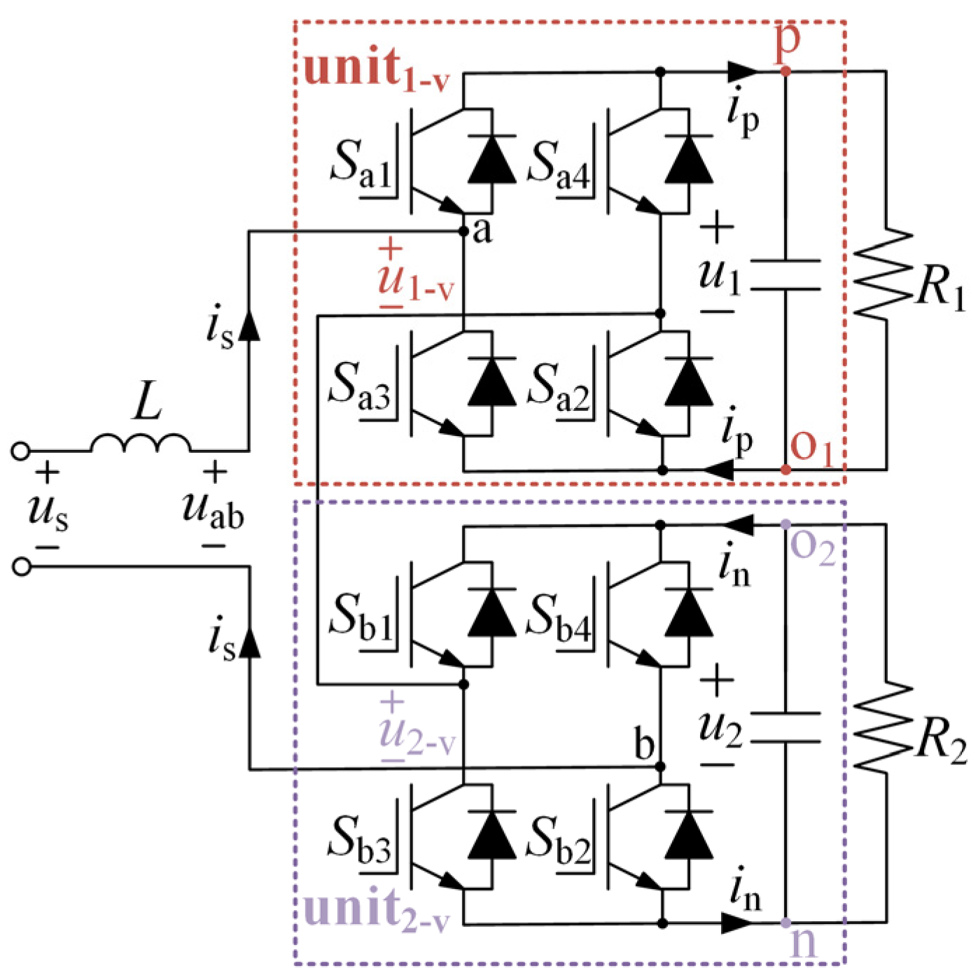
As depicted in Figure 6, node “o” is divided into two separate nodes, “o1” and “o2”. To decouple u1 and u2, the adopted rectifier is replaced with a two-unit H-bridge shown in Figure 6, which shares the same external voltage–current characteristics. The first submodule, referred to as unit1-v, consists of four switches (Sa1, Sa2, Sa3, Sa4) and four diodes, while the second submodule, known as unit2-v, comprises four switches (Sb1, Sb2, Sb3, Sb4) and four diodes. The input ac voltages of submodules unit1-v and unit2-v are u1-v and u2-v, respectively. Sa and Sb are the switching functions for unit1-v and unit2-v, respectively.
The active powers P1 and P2 in (12) represent the input active powers consumed by unit1-v and unit2-v, respectively. These active powers can be expressed in terms of u1-v and u2-v as follows:
P 1 = U 1 - v I s cos ( φ 1 con θ ) 2 P 2 = U 2 - v I s cos ( φ 2 con θ ) 2
where Is, U1-v, and U2-v are the magnitudes of is, u1-v, and u2-v, respectively. φ 1 con and φ 2 con are the phase angles of u1-v and u2-v, respectively. θ is the phase angle of is.
In the H-bridge converter, the peak magnitude of the input ac voltage is lower than that of the dc voltage. As a result, U1-v and U2-v are bound by the following additional constraints:
0 < U 1 - v   0.5 U dc * 0 < U 2 - v   0.5 U dc *
The total input active power of the adopted rectifier is derived as follows:
P total = U ab I s cos ( φ θ ) 2

3.2. Deriving the Voltage Balancing Range

The smaller resistor between the two equivalent loads is denoted as “Rmin” and the larger one is referred to “Rmax”. The level of dc load imbalance, denoted as λ, is defined as follows:
λ = 1 R min 1 R min + 1 R max
In (16), as the level of imbalance between the two equivalent loads increases, the value of λ also increases, serving as an indicator of the internal dc load imbalance.
For convenience in analysis, we assume that “R1” represents “Rmin” and “R2” represents “Rmax”. Consequently, R1 consumes more than half of the total input active powers, expressed as follows:
1 2 P total P 1 P total
In the ideal balance control range of the selected rectifier, u1 and u2 converge to U dc * /2. As a result, the dc load imbalance level “λ” can be expressed as follows:
λ = P 1 P total
By referring to (17) and (18), an approximate range of λ can derived as 0.5 < λ < 1.
Substituting (8) into (12), the active power absorbed by the Rmin in a cycle can be expressed as follows:
P 1 = 1 T 1 0 T 1 ( 1 2 U dc * ) u ref ( 2 d z + 1 ) i s d t
In order to maintain modulation signals within the linear modulation region, the restriction imposed by nonlinear modulation signals in (7) can be expressed as follows:
d z ± u ref 1
By applying (20) into (19), the active power absorbed by Rmin indicates λmax. Subsequently, using (15), (18), and (19), the upper limit of the dc load imbalance level can be calculated. Furthermore, considering (13), (15), and (17), the constraints on the magnitudes of u1-v and u2-v in (14) are further narrowed down. The process will be elaborated upon in the subsequent section, employing Method 1 to provide a comprehensive illustration.

4. Methods to Increase Balance Abilities

In this section, the balance abilities of two typical methods, namely Method 1 and Method 2, are elucidated first, and then two methods (Method 3 and Method 4) to extend the balance range of the typical two methods are discussed.

4.1. Method 1: The Basic Form

By referring to (11), the basic form of the offset voltage is written as follows:
d z = sgn u ref i s Δ d
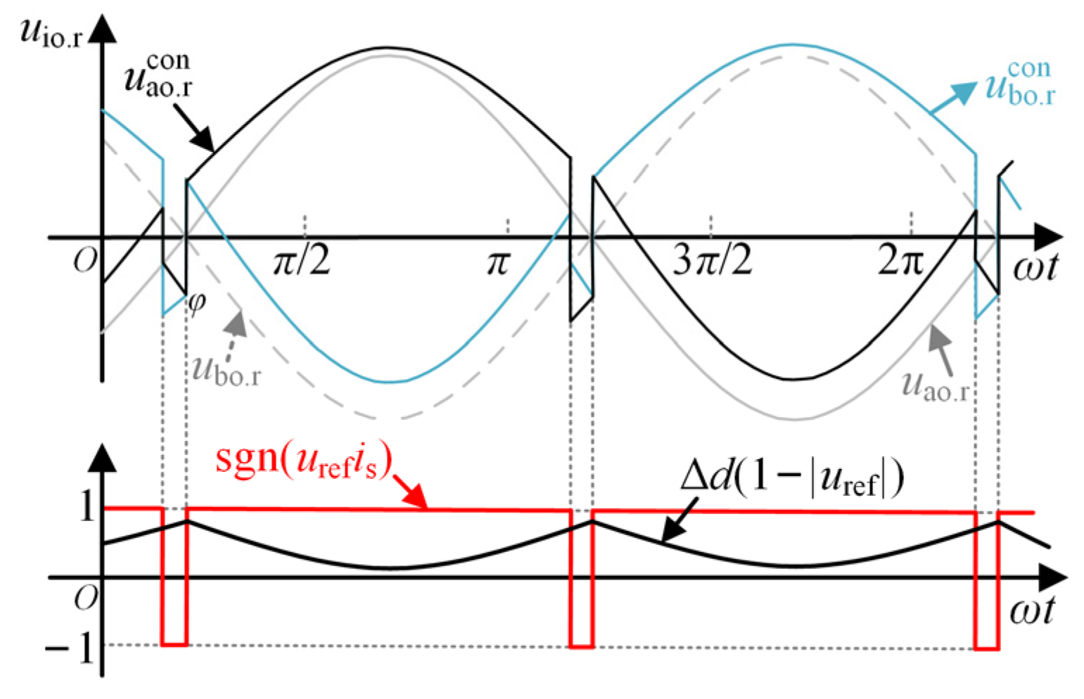
In (21), a square wave is added to the original modulation signals, taking into account the polarity of the grid current and initial signals. The modulation signals of Method 1 are elaborated in Figure 7. For ease of analysis, only waveforms with Δd > 0 are presented in this context. Here, u ao . r con and u bo . r con represent the modulation signals of the converter after implementing Method 1. It is evident that the peaks of the original signals are the most susceptible points on the superimposed modulation signals to exceed the linear modulation region. By substituting (21) into (20) and considering linear modulation, the maximum value of Δd can be derived as follows:
Δ d max = 1 U ref
where Uref is the magnitude of uref.
By applying (21) and (22) into (19), according to (15) and (18), λmax based on Method 1 is described as follows:
λ max = 1 2 + 1 U s cos θ U dc * cos ( φ θ ) 1 2 ( φ θ ) 2 tan ( φ θ ) π
According to (13), (15), (17), (19), and (22), the range of input ac voltage magnitude for each unit based on Method 1 is expressed as follows:
U s cos ( θ ) 2 cos ( φ 1 con θ ) U 1 - v U s cos ( θ ) 2 cos ( φ 1 con θ ) + 1 U s cos ( θ ) U dc * cos ( φ θ ) 1 2 ( φ θ ) 2 tan ( φ θ ) π U s cos ( θ ) cos ( φ 1 con θ ) 0 U 1 - v 0.5 U dc *
U s cos ( θ ) cos ( φ 2 con θ ) 1 2 1 U s cos ( θ ) U dc * cos ( φ θ ) 1 2 ( φ θ ) 2 tan ( φ θ ) π U 2 - v U s cos ( θ ) 2 cos ( φ 2 con θ ) 0 U 2 - v 0.5 U dc *
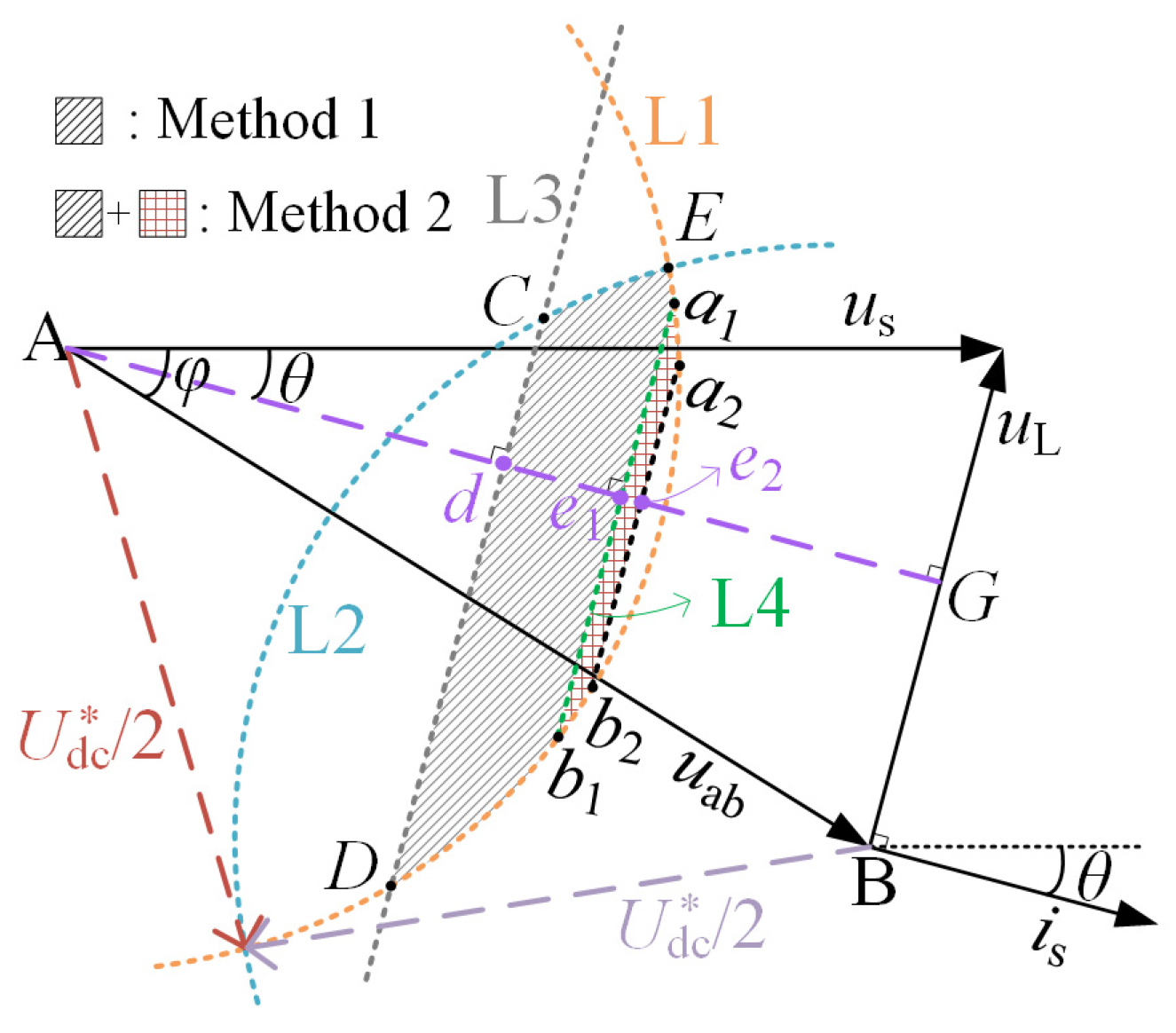
Moreover, by referring to (24) and (25), the range of ac voltage magnitudes for both H-bridge units can be visually represented by a vector diagram depicted in Figure 8. The shaded area “CDb1a1E” enclosed by “L1”, “L2”, “L3”, and “L4” illustrates the balance range of the single-phase 3L-NPC converter. The adopted rectifier is considered controllable when the submodule ac voltages, influenced by the imbalance level of the dc load, fall within this balance range. The curves “L1” and “L2” centered at points A and B with a radius of U dc * indicate the limits on U1-v and U2-v as defined in (14). The straight line “L3”, determined by (17), bisects the line segment AB and is perpendicular to the direction of the grid current vector. The straight line “L4”, representing the constraints imposed by λmax, forms a right angle with the current vector. The line segment AG, parallel to is, intersects the left boundary “L3” of the shadow region at point d and intersects the right boundary “L4” of the shadow region at point e1. The length of segment “de1” indicates the upper limit of the dc load imbalance level (λmax) based on Method 1. The longer the line segment “dd1”, the greater the balance capacity of the corresponding balancing control measures. Thus, the balance abilities are “Method 2 > Method 1”.

4.2. Method 2

The offset voltage devised in [20] is as follows:
d z = 1 u ref sgn u ref i s Δ d
In (26), the modulation signals of Method 2 are depicted in Figure 9. Compared to Method 1, the upward movement of the peaks in Method 2 relative to other points has decreased. Therefore, Method 2 is less balanced.
Substituting (26) into (20), according to linear modulation, the maximum value of Δd is expressed as follows:
Δ d max = 1
Similar to (23), the λmax based on Method 2 can be expressed as follows:
λ max = 3 2 + 2 tan ( φ θ ) 2 ( φ θ ) π + 4 U s cos ( θ ) sin ( φ θ ) 3 π U dc * 8 U s cos ( θ ) 3 π U dc *
Using Equations (13), (15), (17), (19), and (27), the expression for determining the permissible range of input ac voltage magnitudes based on Method 2 can be derived as follows:
U s cos ( θ ) 2 cos ( φ 1 con θ )   U 1 - v 3 2 + 2 tan ( φ θ ) ( φ θ ) π U s cos ( θ ) cos ( φ 1 con θ ) + 4 sin ( φ θ ) 3 π U dc * 8 3 π U dc * U s 2 cos 2 ( θ ) cos ( φ 1 con θ ) 0 U 1 - v 0.5 U dc *
8 3 π U dc * 4 sin ( φ θ ) 3 π U dc * U s 2 cos 2 ( θ ) cos ( φ 2 con θ ) 1 2 + 2 tan ( φ θ ) φ + θ π U s cos ( θ ) cos ( φ 2 con θ ) U 2 - v U s cos ( θ ) 2 cos ( φ 2 con θ ) 0 U 2 - v 0.5 U dc *
The balance range of Method 2 is graphically depicted as the shaded area “CDb2a2E” in Figure 8, as indicated by (29) and (30). As the angle φ 1 con varies, the angle φ 2 con undergoes variations, causing the endpoint of vector u1 (also the starting point of vector u2) to shift within the region “CDb2a2E”. The line segment “a2b2”, which is perpendicular to is, represents λmax and is the upper limit of the balance range based on Method 2. It is clear that the length of line segment “de2” exceeds that of “de1”. Consequently, Method 2 demonstrates a superior balance capacity in comparison to Method 1.

4.3. Method 3: Increasing the Reference DC Voltage

The load imbalance expressions in (23) and (28) clearly demonstrate that adjusting the set value of the dc voltage can result in an elevation in λmax and an expansion of the balancing capacity. By taking (23) in Method 1 as an illustration, the derivative of λmax with respect to U dc * can be expressed as follows:
λ max U dc * = U s cos θ π + 2 tan ( φ θ ) 2 ( φ θ ) π cos ( φ θ ) U dc * 2
Equation (31) is greater than zero. Consequently, as U dc * is increased to U dc con , the balance region for Method 1 can be delineated in Figure 10. Line segment “de1” transforms into line segment “de3”, thereby expanding the balance range and encompassing the shaded area “CFHa3b3GDb1a1E”. The situation pertaining to Method 2 exhibits similarity when U dc * is increased. Consequently, Method 3 proficiently augments the converter’s balance capacity.

4.4. Method 4: Reducing the Total Input Active Power

According to (23) and (28), λmax is solely influenced by the angle “φ” between uab and is, assuming that the angle “θ” between us and is remains unchanged. The only exception to this is U dc * , which has been discussed in the previous subsection. This subsection will now analyze the effect of φ on the system’s balancing capability.
The total input active power can be expressed as follows:
P total = U s I s cos θ 2
As illustrated in Figure 11, the voltage vector of the ac side inductor “uL” consistently remains perpendicular to vector “is”. Thus, the direction of uL remains unchanged due to the constant angle θ. However, as the angle φ undergoes variation, the endpoint B of vector uab is moving along a line aligned with the direction of vector uL, leading to a modification in the magnitude of the is. As a result, according to (32), there is a positive relationship between Ptotal and φ. The angle between uab and is is denoted as (φθ). By adjusting the Ptotal to P s con , the magnitude of uab varies and thereby (φθ) reduced. The vector uab shifts to u ab con .
For instance, considering Method 1, the expression for the partial derivative of λmax with respect to φ can be derived from (23). This partial derivative demonstrates a negative value, indicating that λmax and the range of input ac voltage magnitude of Method 1 can be expanded by reducing the total input active power. This relationship is illustrated in Figure 11. Similarly, when Ptotal is decreased, Method 2 follows a comparable pattern.
Nevertheless, it is important to note that the enhancement in balance ability can only be marginally extended when comparing the methods with and without Method 4. This limitation arises from the presence of a relatively low inductance on the ac side.

5. Comparing Different Approaches for Enhancing Load Balancing Capabilities

In this section, a comparison of the balancing abilities of the previously analyzed methods is presented.
The upper limit of dc load imbalance of the aforementioned methods is presented in Table 1. According to Figure 8, the balance ability of Method 2 is greater than that of Method 1. On the basis of either Method 1 or Method 2, simultaneously employing Method 3 or Method 4 can increase or extend the balance limits. Thus, the balancing abilities of Method 1 and Method 2 are smaller than that of Method 1 + Method 3, Method 2 + Method 3, Method 1 + Method 4, and Method 2 + Method 4. Additionally, enabling Method 4 can only increase the balance ability slightly for the relatively low inductance results in a small phase angle φ, leading to a limited range of movement at the end of uab. Therefore, the order of balancing abilities is “(Method 2 + Method 3) > (Method 1 + Method 3) > (Method 2 + Method 4) > Method 2 > (Method 1 + Method 4) > Method 1”.

6. Simulation Results

In this section, the maximum dc load imbalance level and balance range of these proposed methods are verified by simulation tests. The time domain simulation model of the single-phase 3L-NPC converter is established.
The main system parameters of the model are outlined in Table 2, and these parameters remain consistent across various simulation runs.
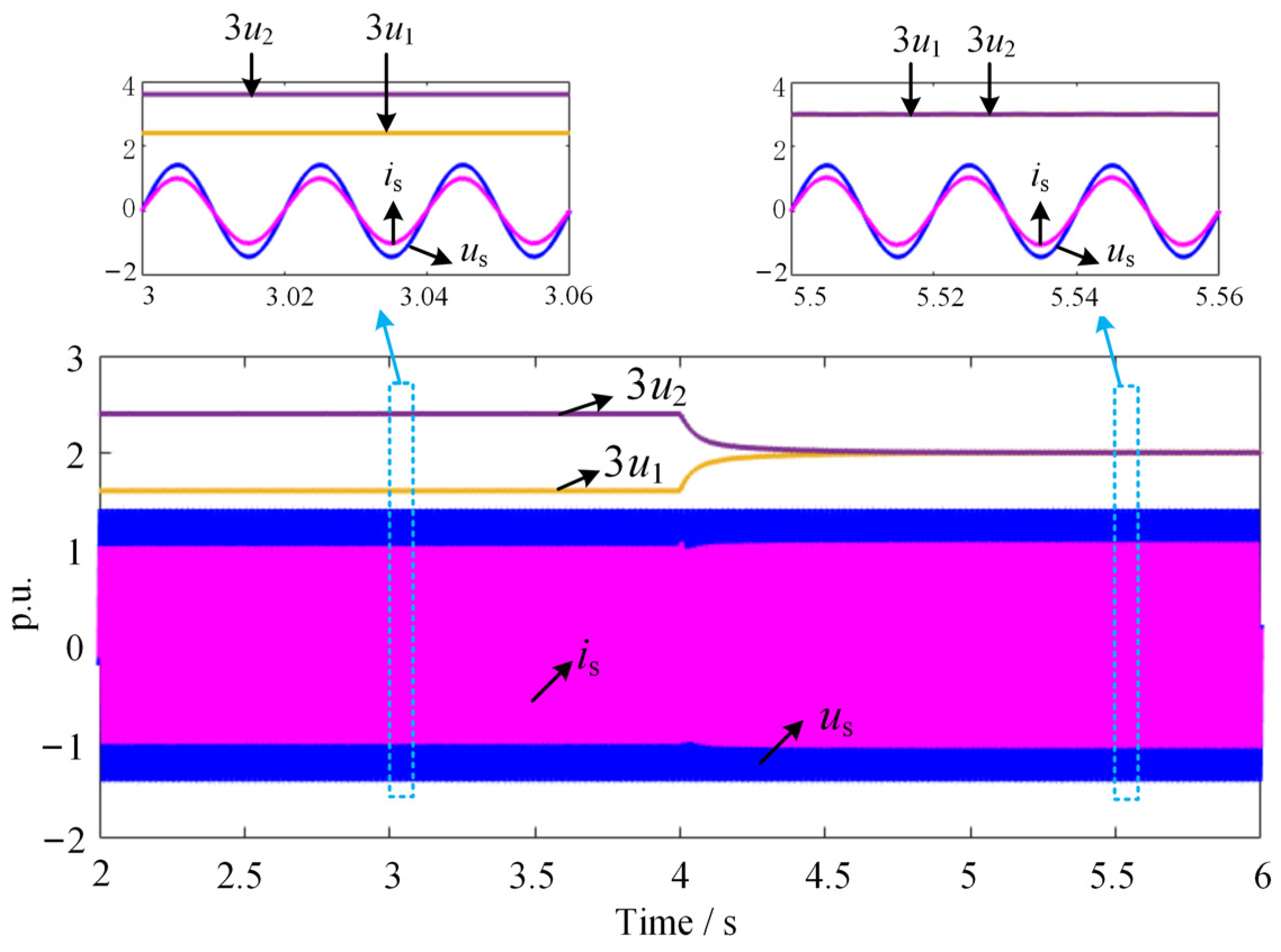
The voltages of the ac source, the dc voltages, and the grid current before and after enabling Method 1 are illustrated in Figure 12. The ac base current, ac base voltage, and dc base voltage are 8 A, 113 V, and 75 V, respectively. The system operates in the unity power factor operating condition both before and after implementing balance control. The THD values of the grid current are measured by the “Powergui FFT Analysis Tool” in Matlab/Simulink, which are 1.96% (without Method 1) and 1.93% (with Method 1).
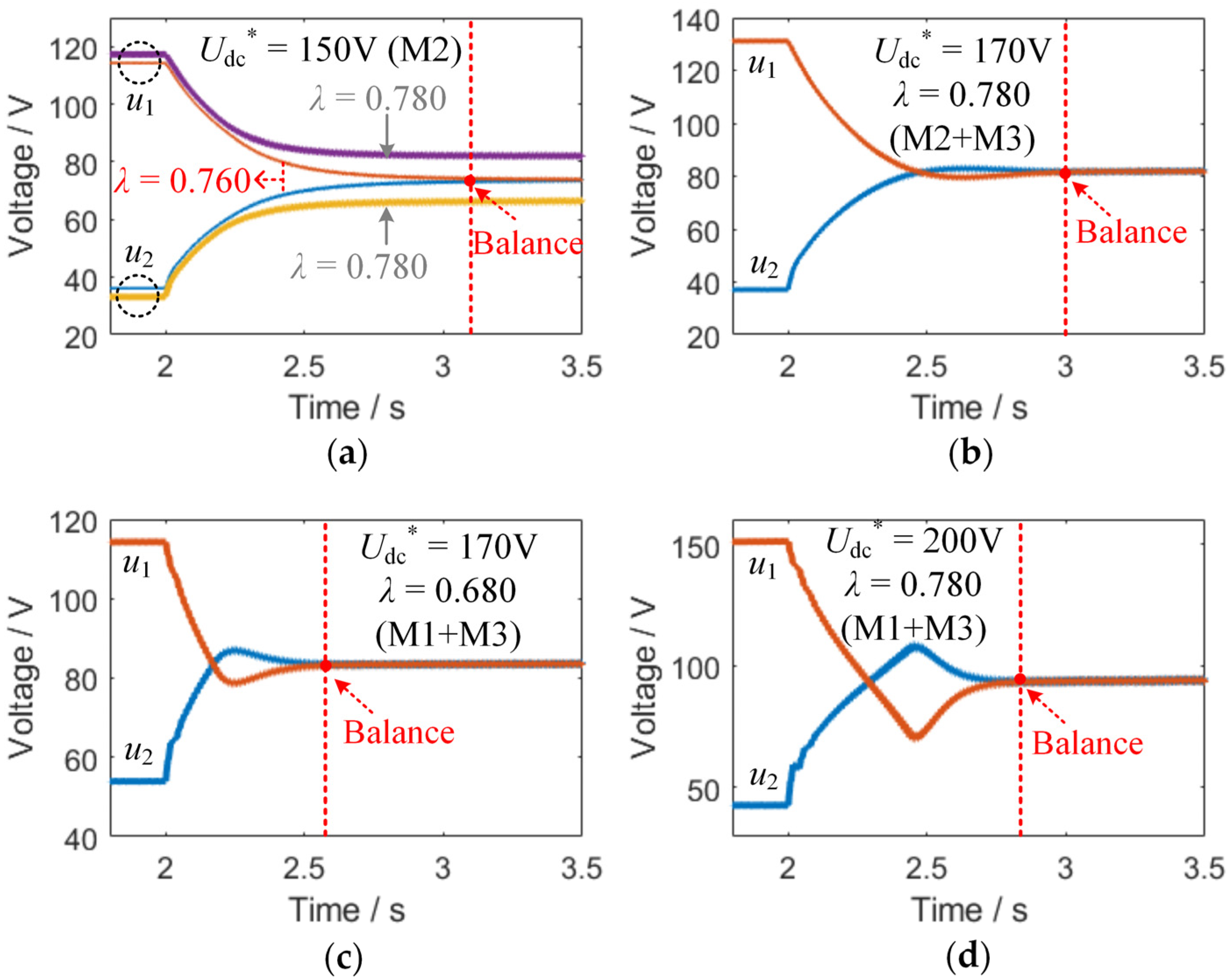
Figure 13 depicts the dc voltages when the rated dc voltage is 150 V and the imbalance level “λ” is 0.600 (R1 = 20 Ω, R2 = 30 Ω) and 0.680 (R1 = 16 Ω, R2 = 34 Ω), respectively. According to Table 1, the “λmax” of Method 1 and Method 2 are 0.665 and 0.770, respectively. In Figure 13a, when “λ = 0.600”, which is lower than both 0.665 and 0.770, both Method 1 and Method 2 reach the voltage balance. Yet, Method 1 is faster than Method 2. On the other hand, in Figure 13b, when “λ = 0.680”, which is higher than 0.665 but lower than 0.770, the dc voltages with Method 1 cannot be balanced, while those with Method 2 are balanced. As illustrated in Figure 14a, the rated dc voltage is still 150 V; yet, the imbalance level “λ” is 0.760 (R1 = 12 Ω, R2 = 38 Ω) and 0.780 (R1 = 11 Ω, R2 = 39 Ω). With Method 2, the voltages are balanced when “λ” is 0.760 (less than 0.770) and unbalanced when “λ” is 0.780 (higher than 0.770). Therefore, their balance abilities are sorted as “Method 2 > Method 1”.
The influence of Udc*on the balance ranges is depicted in Figure 14 b–d. In Figure 14b,c, the rated dc voltage is 170 V and the dc voltages are balanced. When comparing Figure 14c to Figure 13b (both at “λ = 0.680”), the voltages using Method 1 are balanced, as Udc* is increased from 150 V to 170 V. Similarly, when comparing Figure 14b to Figure 14a (both at “λ = 0.780”), the voltages with Method 2 are balanced when Udc* is increased from 150 V to 170 V. Thus, the balance limits of Method 1 and Method 2 are extended when the rated dc voltage is increased. Furthermore, in Figure 14d, the dc voltages are balanced with Method 1 (“λ = 0.780”, Udc* = 200 V), whereas they are not balanced in Figure 1a under the same “λ” and a lower Udc*. Consequently, the balance limit of Method 1 + Method 3 is higher than that of Method 2. Therefore, Method 3 is effective in voltage balancing, and the balance abilities are “(Method 2 + Method 3) > (Method 1 + Method 3) > Method 2 > Method 1”.
Additionally, the results in Figure 13 and Figure 14 are filled in Table 3. It is obvious that dc voltages can be balanced only when the load imbalance level “λ” is less than the upper limit “λmax”. Therefore, the calculations for the balance range are accurate.
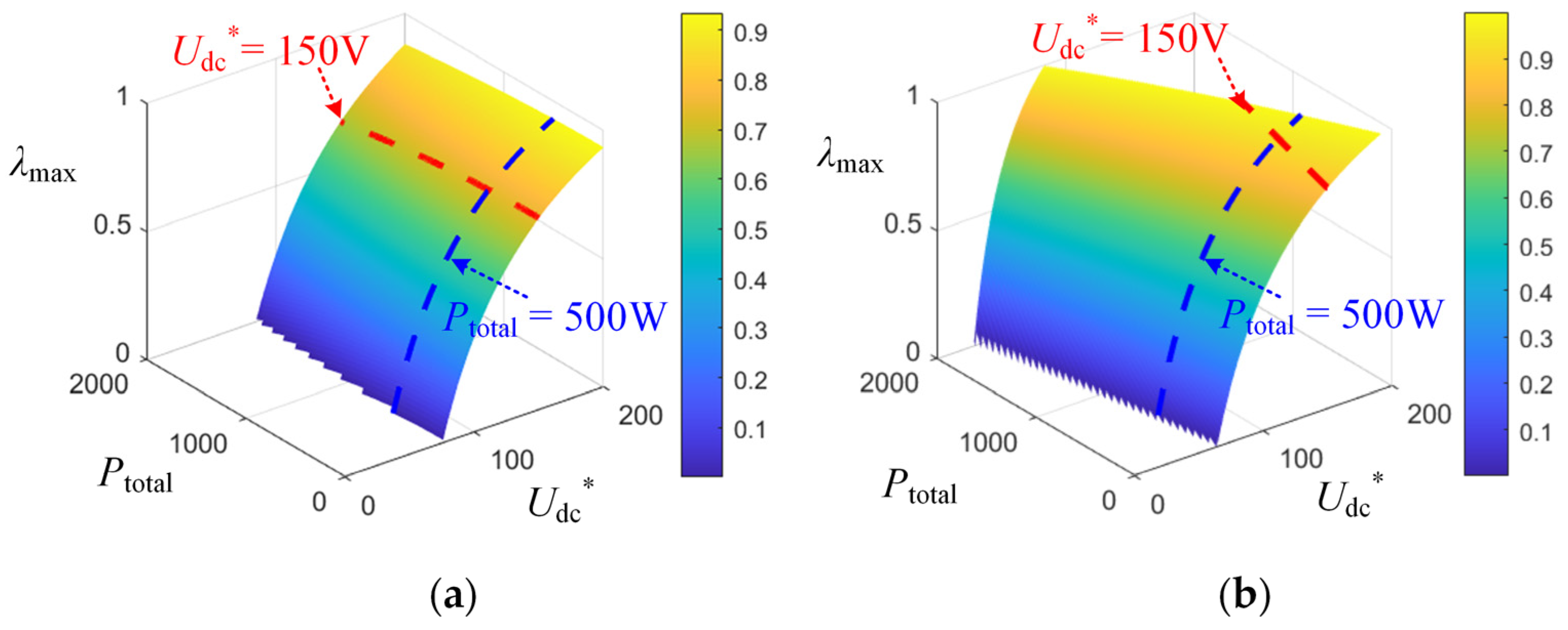
Figure 15 displays the variations in the upper limits “λmax” of Method 1 and Method 2 as the active power “Ptotal” and the rated dc voltage “Udc*” change. The red dashed lines show the variations of λmax with Ptotal when Udc* is 150 V. The blue dashed lines delineate the changes of λmax with Udc* when Ptotal is 500 W. It is evident that the influence of active power on the balancing limits is minimal, making it impractical. Thus, the hierarchy of balancing capabilities is as follows: “(Method 2 + Method 3) > (Method 1 + Method 3) > (Method 2 + Method 4) > Method 2 > (Method 1 + Method 4) > Method 1”.
Nevertheless, while configuring system parameters, there might be a significant dc load imbalance at specific power levels. Consequently, if the rated dc voltage remains constant and the dc load imbalance is substantial, the active power can be temporarily decreased to improve the balancing capacity.

7. Conclusions

This paper presents a quantitative analysis of the balancing range of single-phase 3L-NPC converters by conceptualizing the converter as a two-unit cascaded H-bridge system to decouple u1 and u2. The focus is on the balance control methods based on CBPWM with offset voltage injection. The offset voltage constraint is derived using switching functions (Sa and Sb), and the balancing range of two typical methods for the converter is determined based on power conservation principles. Novel methods are explored to expand the balance range in response to the maximum load imbalance levels of Method 1 and Method 2. A comparative analysis of these methods is conducted to evaluate their balancing capabilities. The accuracy and effectiveness of the balance range calculations are confirmed through MATLAB/Simulink simulations. This study lays a theoretical groundwork to ensure the secure and stable operation of single-phase 3L-NPC converters.

Author Contributions

Conceptualization, methodology, validation, and formal analysis, Z.W. and N.J.; writing—original draft preparation, Z.W.; writing—review and editing, N.J., S.W., J.M. and R.Z.; supervision and project administration, N.J. and S.W.; funding acquisition, S.W., J.M. and T.L. All authors have read and agreed to the published version of the manuscript.

Funding

The funding is provided by the Natural Science Foundation of Sichuan, China (No. 2023NSFSC0301).

Data Availability Statement

The raw data supporting the conclusions of this article will be made available by the authors ([email protected]) on request.

Conflicts of Interest

The authors declare no conflict of interest.

References

  1. Aghabali, I.; Bauman, J.; Kollmeyer, P.J.; Wang, Y.; Bilgin, B.; Emadi, A. 800-V Electric Vehicle Powertrains: Review and Analysis of Benefits, Challenges, and Future Trends. IEEE Trans. Transp. Electrific. 2021, 7, 927–948. [Google Scholar] [CrossRef]
  2. Rafi, M.A.H.; Bauman, J. A Comprehensive Review of DC Fast-Charging Stations with Energy Storage: Architectures, Power Converters, and Analysis. IEEE Trans. Transp. Electrific. 2021, 7, 345–368. [Google Scholar] [CrossRef]
  3. Yaramasu, V.; Dekka, A.; Kouro, S. Chapter 6—Multilevel Converters for Renewable Energy Systems; Academic Press: Cambridge, MA, USA, 2021; ISBN 978-0-323-90217-5. [Google Scholar]
  4. Emissions of Carbon Dioxide in the Transportation Sector. Available online: https://www.cbo.gov/publication/58861#_idTextAnchor051 (accessed on 3 March 2024).
  5. Emadi, A. Advanced Electric Drive Vehicles; CRC Press: Boca Raton, FL, USA, 2014. [Google Scholar]
  6. Blaabjerg, F. Control of Power Electronic Converters and Systems; Academic Press: London, UK, 2018; Volume 2, ISBN 978-0-12-805245-7. [Google Scholar]
  7. Blaabjerg, F.; Yang, Y.; Kim, K.A.; Rodriguez, J. Power Electronics Technology for Large-Scale Renewable Energy Generation. Proc. IEEE 2023, 111, 335–355. [Google Scholar] [CrossRef]
  8. Tang, Z.; Yang, Y.; Blaabjerg, F. Power Electronics-the Enabling Technology for Renewable Energy Integration. CSEE J. Power Energy Syst. 2021, 8, 39–52. [Google Scholar] [CrossRef]
  9. Ma, J.; Song, W.; Wang, S.; Feng, X. Model Predictive Direct Power Control for Single Phase Three-Level Rectifier at Low Switching Frequency. IEEE Trans. Power Electron. 2018, 33, 1050–1062. [Google Scholar] [CrossRef]
  10. Han, P.; He, X.; Ren, H.; Wang, Y.; Peng, X.; Shu, Z.; Gao, S.; Wang, Y.; Chen, Z. Fault Diagnosis and System Reconfiguration Strategy of Single-Phase Three Level Neutral-Point-Clamped Cascaded Inverter. IEEE Trans. Ind. Applicat. 2019, 55, 3863–3876. [Google Scholar] [CrossRef]
  11. Lee, J.-S.; Lee, S.-J.; Lee, K.-B. Novel Switching Method for Single-Phase NPC Three-Level Inverter with Neutral-Point Voltage Control. Int. J. Electron. 2018, 105, 303–323. [Google Scholar] [CrossRef]
  12. Faraji, F.; Mousavi, G.S.M.; Hajirayat, A.; Birjandi, A.A.M.; Al-Haddad, K. Single-Stage Single-Phase Three-Level Neutral-Point-Clamped Transformerless Grid-Connected Photovoltaic Inverters: Topology Review. Renew. Sustain. Energy Rev. 2017, 80, 197–214. [Google Scholar] [CrossRef]
  13. Shults, T.E.; Husev, O.; Blaabjerg, F.; Roncero-Clemente, C.; Romero-Cadaval, E.; Vinnikov, D. Novel Space Vector Pulsewidth Modulation Strategies for Single-Phase Three-Level NPC Impedance-Source Inverters. IEEE Trans. Power Electron. 2019, 34, 4820–4830. [Google Scholar] [CrossRef]
  14. Osawa, C.; Matsumoto, Y.; Mizukami, T.; Ozaki, S. A State-Space Modeling and a Neutral Point Voltage Control for an NPC Power Converter. In Proceedings of the Power Conversion Conference—PCC ’97, Nagaoka, Japan, 6 August 1997. [Google Scholar]
  15. Cobreces, S.; Bordonau, J.; Salaet, J.; Bueno, E.J.; Rodriguez, F.J. Exact Linearization Nonlinear Neutral-Point Voltage Control for Single-Phase Three-Level NPC Converters. IEEE Trans. Power Electron. 2009, 24, 2357–2362. [Google Scholar] [CrossRef]
  16. Stala, R. Application of Balancing Circuit for DC-Link Voltages Balance in a Single-Phase Diode-Clamped Inverter withTwo Three-Level Legs. IEEE Trans. Ind. Electron. 2011, 58, 4185–4195. [Google Scholar] [CrossRef]
  17. Wang, S.; Song, W.; Ma, J.; Zhao, J.; Feng, X. Study on Comprehensive Analysis and Compensation for the Line Current Distortion in Single-Phase Three-Level NPC Converters. IEEE Trans. Ind. Electron. 2018, 65, 2199–2211. [Google Scholar] [CrossRef]
  18. Salaet, J.; Alepuz, S.; Gilabert, A.; Bordonau, J.; Peracaula, J. D-Q Modeling and Control of a Single-Phase Three-Level Boost Rectifier with Power Factor Correction and Neutral-Point Voltage Balancing. In Proceedings of the 2002 IEEE 33rd Annual IEEE Power Electronics Specialists Conference, Cairns, QLD, Australia, 23–27 June 2002. [Google Scholar]
  19. Cobreces, S.; Bueno, E.J.; Rodriguez, F.J.; Salaet, J.; Bordonau, J. A New Neutral-Point Voltage Control for Single-Phase Three-Level NPC Converters. In Proceedings of the 2006 37th IEEE Power Electronics Specialists Conference, Jeju, Republic of Korea, 18–22 June 2006. [Google Scholar]
  20. Song, W.; Feng, X.; Smedley, K.M. A Carrier-Based PWM Strategy with the Offset Voltage Injection for Single-Phase Three-Level Neutral-Point-Clamped Converters. IEEE Trans. Power Electron. 2013, 28, 1083–1095. [Google Scholar] [CrossRef]
  21. Jun, E.; Sangshin-Kwak; Baek, J. Model Predictive Control Method with NP Voltage Balance by Offset Voltage Injection for Single-Phase NPC Converters. In Proceedings of the 2019 IEEE 28th International Symposium on Industrial Electronics (ISIE), Vancouver, BC, Canada, 12–14 June 2019. [Google Scholar]
  22. Etxeberria-Otadui, I.; Lopez-de-Heredia, A.; San-Sebastian, J.; Gaztanaga, H.; Viscarret, U.; Caballero, M. Analysis of a H-NPC Topology for an AC Traction Front-End Converter. In Proceedings of the 2008 13th International Power Electronics and Motion Control Conference, Poznan, Poland, 1–3 September 2008; IEEE: Poznan, Poland, 2008; pp. 1555–1561. [Google Scholar]
  23. De Freitas, I.S.; Bandeira, M.M.; Barros, L.D.M.; Jacobina, C.B.; Dos Santos, E.C.; Salvadori, F.; Da Silva, S.A. A Carrier-Based PWM Technique for Capacitor Voltage Balancing of Single-Phase Three-Level Neutral-Point-Clamped Converters. IEEE Trans. Ind. Applicat. 2015, 51, 3227–3235. [Google Scholar] [CrossRef]
  24. Chen, X.; Huang, S.; Jiang, D.; Li, B. Fast Voltage-Balancing Scheme for a Carrier-Based Modulation in Three-Phase and Single-Phase NPC Three-Level Inverters. J Electr Eng Technol. 2018, 13, 1986–1995. [Google Scholar] [CrossRef]
  25. Jun, E.-S.; Kwak, S. A Highly Efficient Single-Phase Three-Level Neutral Point Clamped (NPC) Converter Based on Predictive Control with Reduced Number of Commutations. Energies 2018, 11, 3524. [Google Scholar] [CrossRef]
  26. Lahooti Eshkevari, A.; Mosallanejad, A.; Sepasian, M.S. Design and Analysis of a Simple Predictive Power Controller for a 1.0-kV Single-phase NPC PWM Rectifier. Circuit Theory Apps. 2018, 46, 2495–2511. [Google Scholar] [CrossRef]
  27. Lee, J.-S.; Kwak, R.; Lee, K.-B. Novel Discontinuous PWM Method for a Single-Phase Three-Level Neutral Point Clamped Inverter with Efficiency Improvement and Harmonic Reduction. IEEE Trans. Power Electron. 2018, 33, 9253–9266. [Google Scholar] [CrossRef]
  28. Ma, J.; Song, W.; Wang, X.; Blaabjerg, F.; Feng, X. Low-Complexity Model Predictive Control of Single-Phase Three-Level Rectifiers with Unbalanced Load. IEEE Trans. Power Electron. 2018, 33, 8936–8947. [Google Scholar] [CrossRef]
  29. Guemez, J.G. Modelling and Control of Grid-Tied NPC Inverters. Ph.D. Thesis, University of Southampton, Southampton, UK, 2020. [Google Scholar]
  30. Jun, E.-S.; Nguyen, M.H.; Kwak, S. Model Predictive Control Method Based on Deterministic Reference Voltage for Single-Phase Three-Level NPC Converters. Appl. Sci. 2020, 10, 8840. [Google Scholar] [CrossRef]
  31. Vazquez, S.; Acuna, P.; Aguilera, R.P.; Pou, J.; Leon, J.I.; Franquelo, L.G. DC-Link Voltage-Balancing Strategy Based on Optimal Switching Sequence Model Predictive Control for Single-Phase H-NPC Converters. IEEE Trans. Ind. Electron. 2020, 67, 7410–7420. [Google Scholar] [CrossRef]
  32. Liu, Y.; Mao, X.; Ning, G.; Dan, H.; Wang, H.; Su, M. Model Predictive-Based Voltage Balancing Control for Single-Phase Three-Level Inverters. IEEE Trans. Power Electron. 2021, 36, 12177–12182. [Google Scholar] [CrossRef]
  33. Chowdhury, M.R.; Chowdhury, S.; Rahman, M.A.; Islam, M.R. Advanced Switching Sequences Based Model-Predictive Control for Single-Phase NPC Converters. IEEE Trans. Ind. Electron. 2022, 69, 3515–3526. [Google Scholar] [CrossRef]
  34. Pou, J.; Pindado, R.; Boroyevich, D. Voltage-Balance Limits in Four-Level Diode-Clamped Converters with Passive Front Ends. IEEE Trans. Ind. Electron. 2005, 52, 190–196. [Google Scholar] [CrossRef]
  35. Rivera, S.; Wu, B.; Kouro, S.; Yaramasu, V.; Wang, J. Electric Vehicle Charging Station Using a Neutral Point Clamped Converter with Bipolar DC Bus. IEEE Trans. Ind. Electron. 2015, 62, 1999–2009. [Google Scholar] [CrossRef]
  36. Vazquez, S.; Leon, J.I.; Carrasco, J.M.; Franquelo, L.G.; Galvan, E.; Reyes, M.; Sanchez, J.A.; Dominguez, E. Analysis of the Power Balance in the Cells of a Multilevel Cascaded H-Bridge Converter. IEEE Trans. Ind. Electron. 2010, 57, 2287–2296. [Google Scholar] [CrossRef]
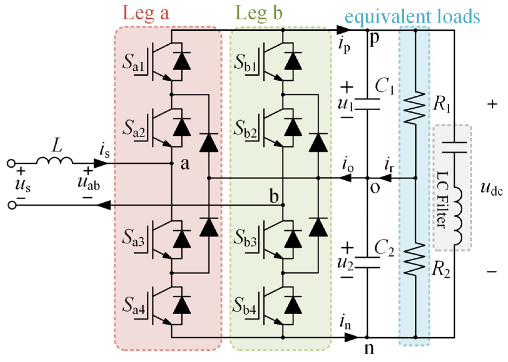
Figure 1. Structure of the single-phase 3L-NPC converter.
Energies 17 01464 g001
Figure 2. The traditional carrier-based pulse width modulation (CBPWM) in a switching cycle (0 ≤ uref ≤ 0.5): (a) switching states (Sa, Sb); (b) duration of switching states.
Energies 17 01464 g002
Figure 3. E and equivalent circuits for states in a switching period when 0 ≤ uref ≤ 0.5: (a) (Sa, Sb) = (1, 0); (b) (Sa, Sb) = (0, −1); (c) (Sa, Sb) = (0, 0).
Energies 17 01464 g003
Figure 4. Equivalent circuit and vector diagram on the ac side: (a) equivalent circuit; (b) vector diagram.
Energies 17 01464 g004
Figure 5. Control strategy of the system.
Energies 17 01464 g005
Figure 6. The two-unit H-bridge equivalence to the adopted rectifier.
Energies 17 01464 g006
Figure 7. Modulation signals of Method 1 (Δd > 0).
Energies 17 01464 g007
Figure 8. Balance range of Method 1 and Method 2.
Energies 17 01464 g008
Figure 9. Modulation signals of Method 2 (Δd > 0).
Energies 17 01464 g009
Figure 10. Balance range is extended using Method 3.
Energies 17 01464 g010
Figure 11. Balance range with reducing the input active power (Method 4).
Energies 17 01464 g011
Figure 12. The voltages and currents during operation at unity power factor.
Energies 17 01464 g012
Figure 13. DC voltages with “Udc* = 150 V”: (a) Method 1 (M1) and Method (M2) with “λ = 0.600”; (b) Method 1 (M1) and Method (M2) with “λ = 0.680”.
Energies 17 01464 g013
Figure 14. DC voltages with methods: (a) Method 2 (M2) with “λ = 0.760” and “λ = 0.780” (Udc* = 150 V). (b) Method 2 + Method 3 (M2 + M3) with “λ = 0.780” and “Udc* = 170 V”. (c) Method 1 + Method 3 (M1 + M3) with “λ = 0.680” and “Udc* = 170 V”. (d) Method 1 + Method 3 (M1 + M3) with “λ = 0.780” and “Udc* = 200 V”.
Energies 17 01464 g014
Figure 15. Upper limit “λmax” varies with Ptotal and Udc*: (a) Method 1; (b) Method 2.
Energies 17 01464 g015
Table 1. The limit of the dc load imbalance level of the methods.
MethodUpper Limit of DC Load Imbalance Level (λmax)
Method 1 1 2 + 1 U s cos ( θ ) U dc * cos ( φ θ ) 1 2 ( φ θ ) 2 tan ( φ θ ) π
Method 2 3 2 + 2 tan ( φ θ ) 2 ( φ θ ) π + 4 U s cos ( θ ) sin ( φ θ ) 3 π U dc * 8 U s cos ( θ ) 3 π U dc *
Method 1 + Method 3 1 2 + 1 U s cos ( θ ) U dc con cos ( φ θ ) 1 2 ( φ θ ) 2 tan ( φ θ ) π
Method 2 + Method 3 3 2 + 2 tan ( φ θ ) 2 ( φ θ ) π + 4 U s cos ( θ ) sin ( φ θ ) 3 π U dc con 8 U s cos ( θ ) 3 π U dc con
Method 1 + Method 4 1 2 + 1 U s cos θ 2 + x 1 2 U dc * 1 2 π arctan ( x 1 U s cos θ ) + 2 x 1 π U s cos θ
Method 2 + Method 4 3 2 8 U s cos θ 3 π U dc * + 2 x 1 π U s cos θ 2 π arctan x 1 U s cos θ
+ 4 U s cos θ 3 π U dc * x 1 U s cos θ 2 + x 1 2
Note: x 1 = 2 P s con U s cos θ ω 1 L U s sin θ .
Table 2. System parameters.
ParametersValue
Switching frequency fs/Hz5000
AC voltage source Us/V 80 2
AC side inductance L/mH5
Load (R1 + R2)/Ω50
DC link capacitor C/mF4.4
Proportional term of balance control Kp1
Integral term of balance control Ki10
Table 3. The results for the methods applied.
MethodUdc*λThe Theoretical Value of λmaxBalance Results
M1150 V0.6000.665Balanced
M1150 V0.6800.665Not Balanced
M1 + M3170 V0.6800.755Balanced
M1 + M3200 V0.7800.855Balanced
M2150 V0.6000.770Balanced
M2150 V0.6800.770Balanced
M2150 V0.7600.770Balanced
M2150 V0.7800.770Not Balanced
M2 + M3170 V0.7800.830Balanced
Disclaimer/Publisher’s Note: The statements, opinions and data contained in all publications are solely those of the individual author(s) and contributor(s) and not of MDPI and/or the editor(s). MDPI and/or the editor(s) disclaim responsibility for any injury to people or property resulting from any ideas, methods, instructions or products referred to in the content.