Abstract
In this manuscript, a direct current (DC) boost converter based on a switched-capacitor circuit with closed-loop control, tailored for applications with high-voltage gain, is introduced. The converter utilizes a network with switching capacitors to enhance voltage gain without relying on inductors, making it ideal for high-voltage scenarios. An active disturbance rejection control (ADRC)-based control scheme is used to maintain output voltage stability in the presence of disturbances. The proposed converter’s functionality and performance are assessed through simulations and experimental tests under various load conditions. A loss analysis, considering the losses from switches and diodes, is provided to determine the net efficiency. The results from both simulations and experiments show that the proposed converter achieves a high-voltage gain, excellent load regulation, and rapid transient response, highlighting its potential for applications that require a high-voltage boosting operation.
Keywords:
SC-BC; DC-DC converter; duty ratio; voltage gain; volt–sec balance; ADRC; observer; controller 1. Introduction
In recent times, there has been a significant increase in the use of energy storage devices in conjunction with renewable energy sources like fuel cells and photovoltaics (PVs). The DC characteristics of such energy sources are the major cause of increasing interest in DC microgrids. In order to maintain a steady supply of energy and balance variations in generation and demand, energy storage electrical systems stores the abundant energy for later use. They are essential for grid stability, backup power, renewable energy systems, and electric vehicles (EVs) [1]. However, these devices frequently produce low voltage, which prompts for high-gain converters to raise it to levels that are usable. Also, the energy produced by PV panels generally have low voltage due to various factors such as partial shading, dirt, lower light intensity, and lower designed efficiency of around 20%, and thus the demand for high-gain DC-DC converters is increasing to optimize the flow of power [2]. The voltage can only be increased by around two to three times the input voltage using a traditional boost converter [3]. If its duty cycle further increases to achieve a higher gain, the system tends towards instability and also, at higher duty cycles, the controller may fail to stabilize the converter. Additionally, using a converter at very high duty cycles (0.9 or above) or very low duty cycles (near 0.1) causes unfavorable nonlinear behavior and decreased efficiency [4,5,6,7]. This issue is addressed and solved in [8] by designing a Luo super-lift-based converter consisting of many switches. However, this converter has significantly increased switching losses and could achieve a voltage gain of up to around 10 only. Some authors have used a transformer in the circuit of the converter to achieve a higher gain, as in the flyback converter explained in [9]. Their circuit becomes bulky and costly with the use of a transformer, Also, the converter’s overall efficiency decreases due to the presence of leakage inductance in the transformer.
Researchers attempted to achieve higher gains by eliminating the transformers using non-isolated inductors in [10,11]. In [10], the efficiency of the converter is claimed to be around 92%. Also, the cost of the converter is high due to the presence of two high-frequency inductors. This problem is also faced by the converter in [11] as it has two coupled inductors. Also, this converter has an efficiency of around 92.7%. Some authors have achieved high gains by cascading various individual converter stages [12,13,14]. However, with the cascading phenomenon, the losses increase, resulting in reduced efficiency. In the literature, switched-capacitor-based boost converters (SC-BCs) are receiving tremendous attention from researchers for harvesting energy with a high-voltage gain from non-conventional sources [15,16]. These are hybrid types of converters that do not contain bulky transformers and give much-improved efficiency [16,17,18,19,20]. The main aim of the design of hybrid SC-BC converters is to multiply the input voltage with a network consisting of some switches and capacitors and then feed this voltage to a boost converter, thereby increasing the voltage gain to a larger value. The author in [21] developed a model of a high-gain switched-capacitor-based boost converter without the need of any inductor. However, due to the absence of an inductor, the input current rises instantly during the transient phase. This leads the input source to enter a constant current mode. This may be harmful to the devices connected at the output of this converter. In [22], the author proposed a model of a switched-capacitor-based boost converter consisting of many diodes and MOSFETs. The above-said circuit is further modified by replacing all the diodes with the MOSFETs to eliminate the voltage drops in the diodes [23]. However, this modified circuit contains many switches, that may result in poor efficiency at higher switching frequencies (due to switching losses in the MOSFETs). In [24], a switched-capacitor-based boost converter circuit was designed by the author for high-voltage gain applications with three duty ratios and an efficiency of 93.4%. Nonetheless, the use of three duty ratios makes the controllability of the said converter quite complex.
It has been seen that authors in the previously reported works have focused on the design of switched-capacitor-based converters to achieve a higher gain without considering their closed-loop control. However, it is impossible to achieve a fixed DC voltage at the output of the converter in the presence of unwanted disturbances (varying load, varying input, noise, etc.). Designing control laws for SC-BC converters is a great challenge to researchers, as these circuits are highly nonlinear and exhibit inverse response characteristics. In the present manuscript, a novel switched-capacitor-based boost converter consisting of three diodes, five MOSFETs, three capacitors, an inductor, and a load resistor is proposed. The key advantage of the designed converter is that a substantial voltage gain can be obtained by operating the switches together with two different duty ratios. This concept of two-duty ratios facilitates the user to achieve a substantially high gain without the use of an extreme duty ratio. Furthermore, the active disturbance rejection control (ADRC) is applied to the proposed converter to achieve its stable closed-loop operation. ADRC is an advanced control technique that estimates the disturbances as a separate variable and suppresses them in real time [25,26,27,28,29]. The robustness of the proposed controller towards variations in the reference voltage, input signal, and load resistance is verified through simulations and experiments. The main contributions of this work are therefore summarized as follows:
- A novel switched-capacitor-based boost converter is proposed that provides a high-voltage gain.
- The gain of the proposed converter is calculated and found to be higher than a conventional boost converter and the converters in [10,11,24].
- The recommended converter is controlled using an ADRC technique to achieve a stable and fixed DC under varying loads and environmental conditions increasing its suitability for renewable energy applications.
- Loss analysis for the circuit is performed for four different loads and efficiencies of more than 94% are achieved.
This paper has been organized in the following way. Section 2 describes the principle of operation of the proposed converter. A brief description of the mathematical modeling for the converter is given in Section 3. The performance characteristics are explained in Section 4. Section 5 describes the design and tuning method for the ADRC-based controller. Section 6 describes the results obtained from the simulation and experimental setups. Furthermore, a loss analysis is also performed which is analyzed in Section 7. The conclusion is derived in Section 8.
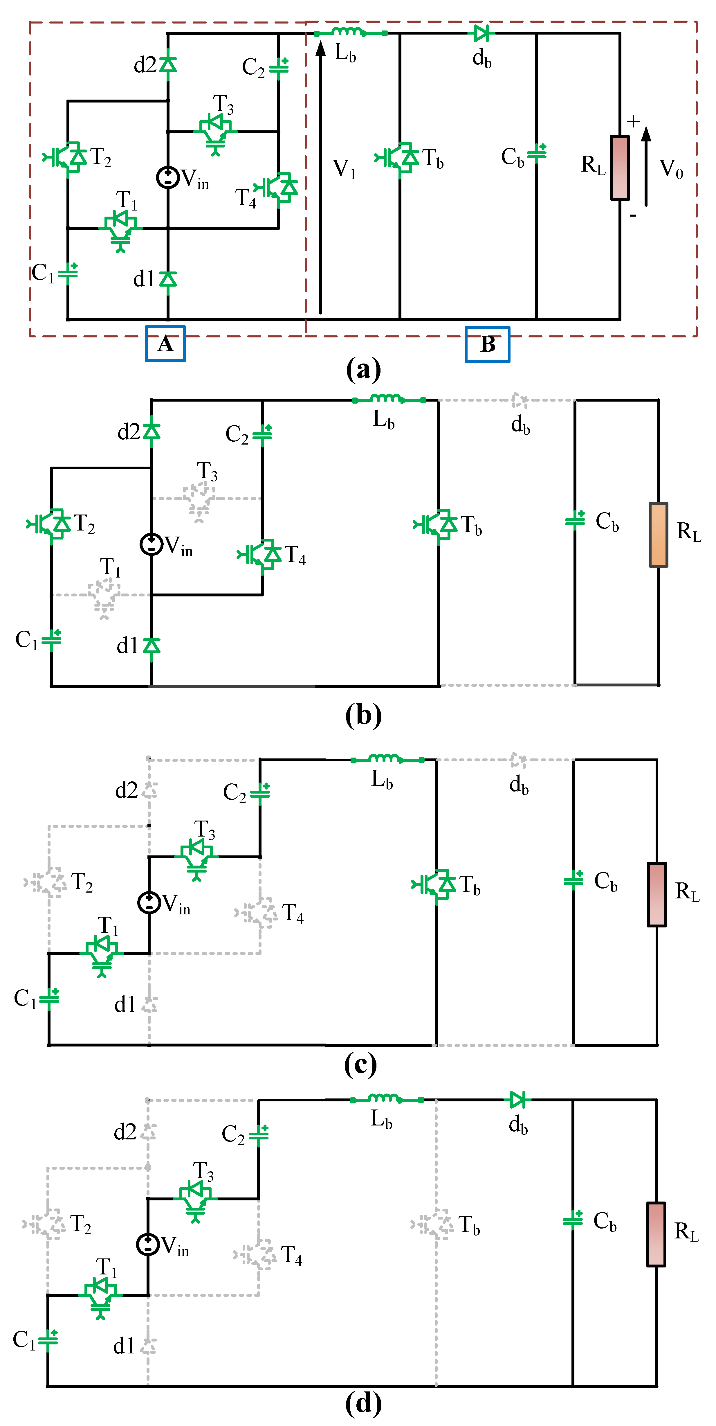
2. Proposed Circuit
The complete structure of the proposed switched-capacitor (SC)-based boost converter circuit is shown in Figure 1a. This is a hybrid structure consisting of a switched-capacitor circuit and a boost-converter circuit arranged in a cascaded manner. With the aid of the capacitors, the first stage of the circuit, which consists of a network of switched capacitors, doubles the input voltage. The second stage then increases the input voltage and transfers the energy to the load side with an enhanced output voltage. In the switched-capacitor circuit, there are four MOSFETs (, , , and ), two diodes ( and ), and two capacitors ( and ). The boost converter circuit has an inductor (), a capacitor (), a MOSFET (), a diode (), and a load resistance (). The diode voltage drop is denoted by which is approximately 0.7 V. There is no such voltage drop in the case of the MOSFETs. There are three different modes in which the circuit can function:

Figure 1.
Proposed SC-based DC-DC converter. (a) Complete circuit diagram. (b) Mode 1 operation (time interval (zd)*: , , , and are being charged). (c) Mode 2 operation (time interval (1 − z)d: capacitors are connected in series and is charged to higher voltage). (d) Mode 3 operation (time interval (1 − d): is discharged and output voltage is boosted).
The time span of the first mode is , where z is the charging duty cycle of the switched-capacitor circuit over the span . The duration of the second and third modes are and , respectively. The circuit diagram of the first mode of operation is depicted in Figure 1b. In this mode, MOSFETs , , and are switched ON while MOSFETs and are kept OFF. The voltage across both the capacitors and keeps rising. In the meantime, the load voltage is supplied by the capacitor , which discharges through the load resistance . In the second stage, as depicted in Figure 1c, the MOSFETs , , and are switched ON while keeping the MOSFETs and OFF. This mode charges the inductor with a voltage three times the input voltage by connecting the voltages across the capacitors and the source in series. On the load side, the capacitor still discharges through the load as in the first stage. In the third stage, only the MOSFET is switched OFF keeping the other circuit conditions as they were in the second stage. Here, the stored energy in the capacitors combined with the stored energy in the inductor and voltage source is plunged to the capacitor , so that the output voltage is increased in comparison with the input voltage depending on the duty ratio of . Also, the load resistor is supplied by the load current through the input source.
3. Mathematical Modeling of Proposed Converter
As mentioned in the previous section, the SC-BC has three modes of operation. The differential equations are obtained independently in these three modes of operation. To obtain the combined differential equation, the state-space averaging technique is used. The diode voltage drop is considered to be 0.7 V. The internal resistance of the source voltage () is designated while that of the inductor is designated . The internal resistance of MOSFET is very small and is neglected. The value of the capacitances in the switched-capacitor circuit is equal and can be denoted by C. Also, the voltage across these capacitors will be equal and is denoted by .
3.1. Mode 1
3.2. Mode 2
3.3. Mode 3
To combine the three modes in a complete interval the state-space averaging technique is used such that the three modes are summed up by multiplying with , , and , respectively. The averaged Equations (10)–(12) are given as follows:
Small signal analysis can be carried out by introducing a small perturbation on all the state variables. However, in order to develop the model, smaller perturbations are ignored, keeping only the average values of the variables such as , , , , , and .
Hence, these changes are substituted into Equations (10)–(12) to obtain a large signal model in Equations (13)–(15) written below as follows:
Under steady-state conditions, the above time derivatives may be equated to zero. Therefore, we have the following (16):
The diode voltage drop may be nullified by replacing diodes with MOSFETs.
3.4. Small Signal Modeling of the Developed Converter
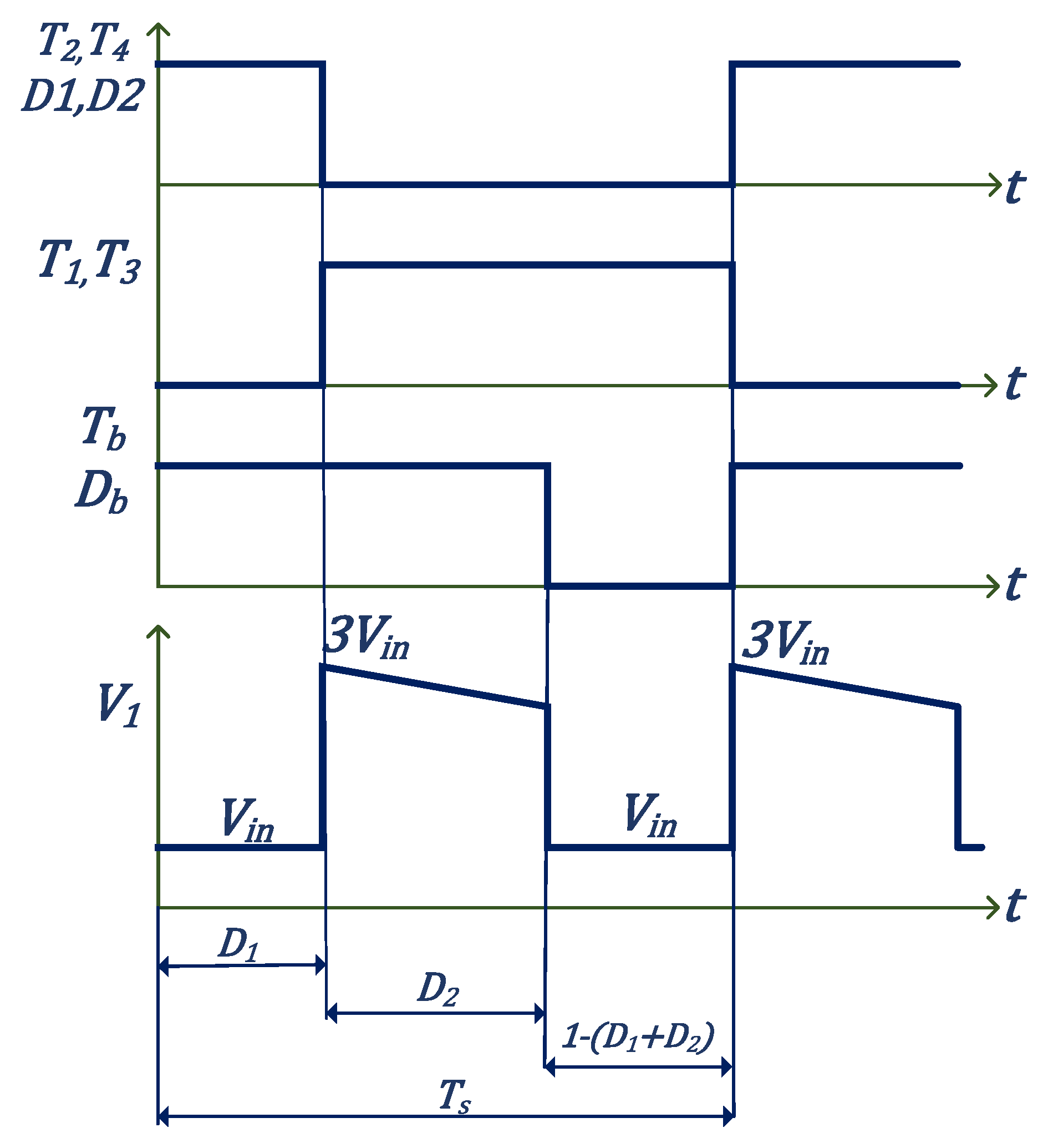
The three modes of the converter are explained by assuming the duty ratio of all three modes as , , and , respectively. The timing diagram depicting all the modes is shown in Figure 2. This figure also depicts the ON and OFF times of each switch and diode. Neglecting the diode voltage drop, the averaged model of the suggested converter using Equations (1)–(9) in terms of and is given as follows:
where . The small signal model could be derived by perturbing each of the variables in Equation (18). The perturbed variables could be depicted as .
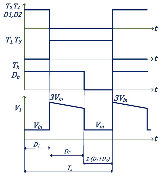
Figure 2.
Timing diagram depicting all the modes.
The above perturbations are substituted in Equation (18) and the steady-state parts are removed. Hence, the small signal model of the designed converter is obtained as follows:
This equation can be written in simplified form as follows:
where the matrices A, , , and are stated in Equation (19). This equation may be used to obtain the transfer function of the circuit in the terms of different variables such as , , and independently.
3.5. Gain Calculations by Volt–Sec Balance of Inductor
The differential equation of the inductor current with respect to time is written for all three modes and, finally, the volt–sec balance is applied over a time period.
Mode 1: Consider that mode 1 operates for a period of , where is the duty cycle of the switches corresponding to the first mode. Kirchhoff’s voltage law (KVL) is applied to the loop containing the inductor which results in the following:
Mode 2: Mode 2 is assumed to occur for a period of , where is the duty cycle of the switches corresponding to the second mode. Hence, applying the KVL across the inductor results in the following equation:
Mode 3: The third mode occurs for a time span of . The KVL equation for the inductor is given by the following:
The volt–sec balance equation across the inductor for the complete time period is given by the following:
Therefore,
It is presumable in the steady condition that . Hence, the voltage gain equation is calculated as follows:
4. Comparison of the Proposed Converter’s Performance
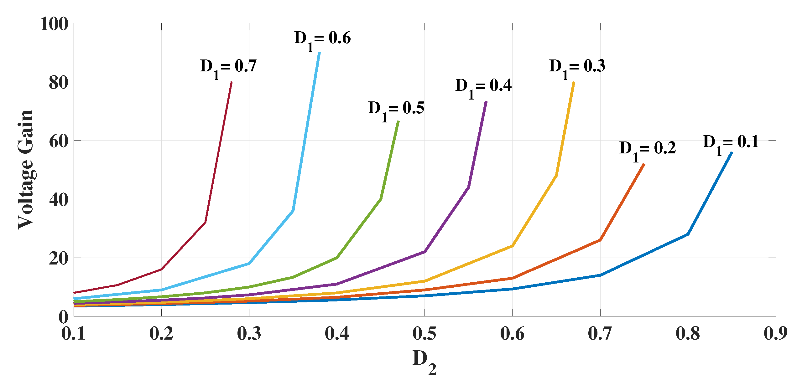
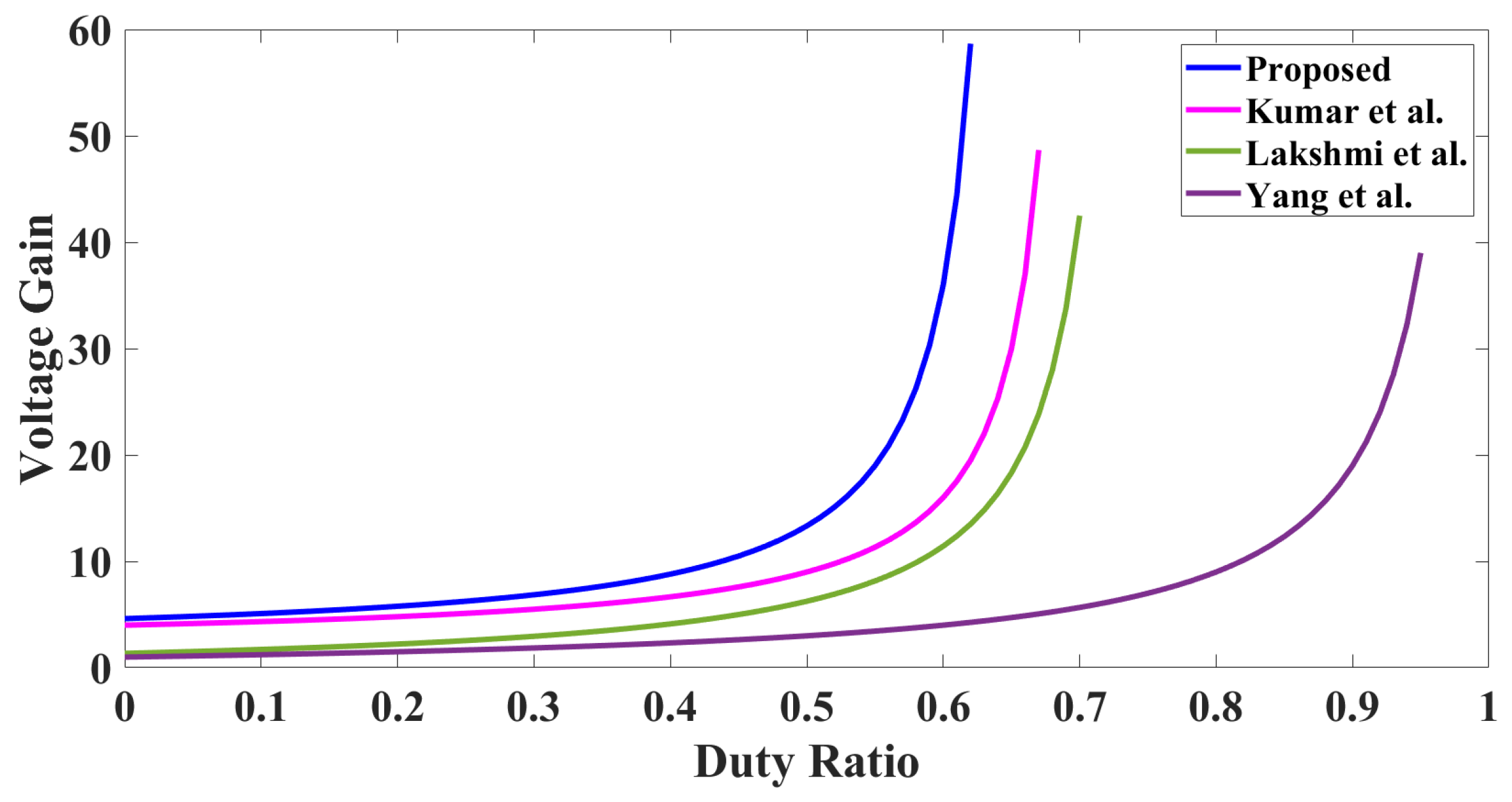
Equation (25) provides the introduced converter’s voltage gain. The gain depends on as well as . The effect of and on the gain is observed by varying for a fixed value of and the response hence obtained is plotted as depicted in Figure 3. Here, different values of are selected and, at these values, the effect of varying is studied on the gain. As the value of increases, the curve shifts from right to left. A few alternative converters shown in [10,11,24] are compared with the proposed converter’s various performance attributes. A gain of 46 is achieved at and while, for , , and , the converter in [24] produces a gain of 31. The converter presented in [10] attains its maximum gain of around 35 while the proposed converter achieves its highest gain of 95. Figure 4 displays the gain’s comparison of the various converters and proves that the presented converter achieves the highest gain. Table 1 compares the voltage gain, voltage stress, and several other components of the proposed converter with those of existing converters. On comparing with the other converters, it is found that the suggested converter is capable of achieving much higher gain for the same values of duty ratios. The voltage stress on the diodes and switches is comparable to that of the converter in [10] and lower than that of the traditional boost converter. Also, fewer inductors are needed to generate a comparably larger gain. Furthermore, the theoretical efficiencies of the various converters are also compared and listed in Table 1. The efficiency of the developed converter is calculated in Section 7. The advocated converter’s theoretical efficiency is around 96 % and is higher than the converters in [10,11,20].
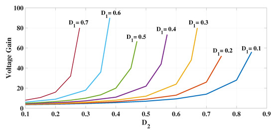
Figure 3.
Plot for voltage gain vs. with different .
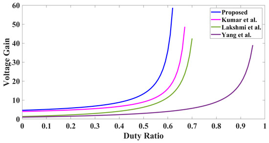
Figure 4.
Comparison of gain of proposed topology and topologies in [10,11,24].

Table 1.
Comparison of presented and existing converters.
5. ADRC-Based Control of the Proposed Converter
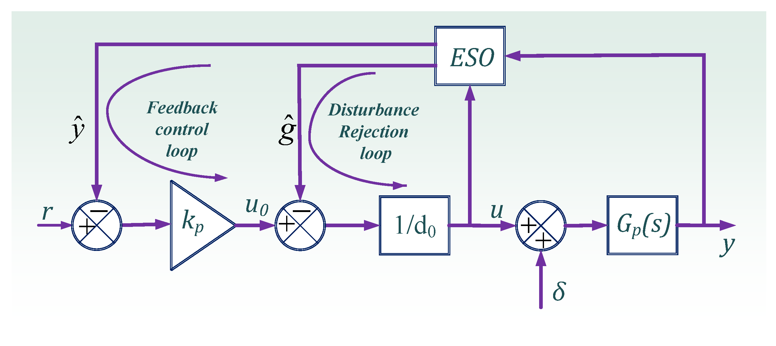
For practical applications, there is a need for regulated output from the converter. In order to obtain the intended output from the converter, a closed-loop control framework is required. All robustness and stability requirements are met by the active disturbance rejection control approach. The disturbance variable’s estimation and its real-time suppression or rejection form the basis of the ADRC approach [29,30]. The fundamental block diagram of the closed-loop ADRC control structure is shown in Figure 5.
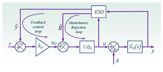
Figure 5.
A closed-loop ADRC control block schematic diagram.
In this figure, y is the obtained output, is the output estimate, is the estimate of the disturbance comprising the unmodeled dynamics and external and internal disturbances, and r is the reference. The controller’s gain is denoted by . Furthermore, corresponds to the transfer function of the developed converter, the external disturbance is denoted by , and u is the final control signal. The extended state observer (ESO) differentiates the output and the disturbance signal, and estimates them separately. Further, the disturbance is canceled by the selection of a proper controller.
The modeling of the converter’s section B is conducted independently in order to use the control approach on the converter in an appropriate manner. The control signal provided by the controller drives the switch (). The transfer function of section B of the converter is derived and formulated by Equation (27):
5.1. Controller Design
Equation (28) represents the conversion of the transfer function of the converter derived from Equation (27) into the time domain:
where and are the numerator’s coefficients, indicating the dynamics of the zeroes, and and are the denominator’s coefficients in the real transfer function, showing the pole dynamics. The system’s gain is denoted by , and any inaccuracy in the presumption of is represented by . represents the external disturbances. Equation (28) can be summarized by Equation (29) as follows:
where
In Equation (31), the pole dynamics are represented by , whereas all the disturbances and unmodeled dynamics are represented by . Once more, g may be expressed as in Equation (32):
Since , can be given by Equation (34):
With the aforementioned presumptions, the state-space Equation (36) is constructed as follows:
where , , , and are the state matrices of the proposed high-gain converter.
The observer is intended for the system described above, as seen in Equation (37):
Here, the observer’s state variable is denoted by , is the observer’s gain, and ‘T’ stands for the matrix’s transposition.
The third-order observer’s characteristic equation may be constructed with poles assigned to . This would lead to Equation (38) as follows:
A proportional derivative type controller is selected to reject the disturbance term in real time as given by Equation (42) as follows:
where and .
The characteristic equation of a controller may be constructed with poles assigned to . This would lead to Equation (43) as follows:
The above equation results in and . Equation (44) provides the controller’s transfer function as follows:
5.2. Frequency Domain Analysis and Parameter Tuning
Stability analysis can be performed for the closed-loop system by using Equations (36), (37), and (42) as given by Equation (45):
where and . Now, using an equivalence transformation , where , the state estimation Equation (45) is now given by Equation (46):
To fulfill the criteria of BIBO stability, the eigen values of Equation (46) must be in the left half plane. Here, the scaled reference and are always bounded and the condition of stability is only dependent on , which means that should be differentiable [31].
The selection of tuning parameters is a crucial part of the closed-loop performance of the system. The author of [31,32] gave specific guidelines for the selection of the controller’s and observer’s bandwidths. Based on this, the controller’s and observer’s bandwidths were selected as rad/s and rad/s. Accordingly, the values of the controller’s and observer’s gains were calculated.
The closed-loop system’s stability can be proved by drawing the Bode plot as shown in Figure 6. This figure clearly demonstrates that the closed-loop system is stable with gain and phase margins at 20.1 dB and 71.9 degrees respectively.
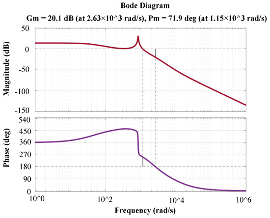
Figure 6.
Bode plot of the closed-loop system.
6. Simulation and Experimental Results
To analyze the servo and regulatory performances, simulations and experimental verifications are carried out. Additional research is conducted on the regulatory performance in relation to the input voltage and load resistance fluctuations.
6.1. Simulation Results
The simulation was carried out by utilizing the Simscape power system toolkit and the MATLAB/Simulink 2021a platform. Table 2 displays the circuit’s specs.
Table 2.
Specifications for the developed converter’s circuit.
The discrete mode of operation was used for the control system design. The simulation study is performed under various scenarios consisting of input voltage and load fluctuations.
Figure 7 shows the diagram for the output voltage, input voltage, load current, and duty cycle following a momentary variation in the reference voltage. In this case, the input voltage is set to 5 V and a 100 fixed resistor is used. The variation in reference voltage is performed in various steps as 12 V-15 V-20 V and then back to 20 V-15 V-12 V. The response from Figure 7 shows that the output voltage adjusts to match the reference voltage as it fluctuates due to the adjustment of the duty ratio provided by the controller with a settling time of 0.02 s. The output current also settles to a new value with the settlement of the output voltage. Here, it can be noticed that the output of 20 V is obtained at a duty ratio of 0.4 proving the converter exhibits high gain.
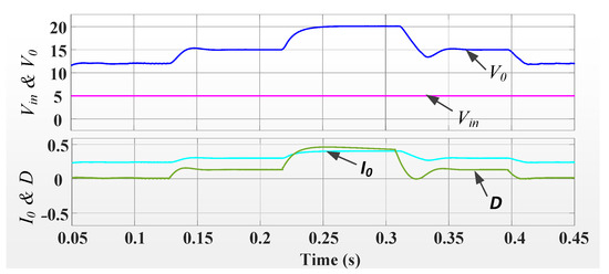
Figure 7.
Output voltage response for varying reference.
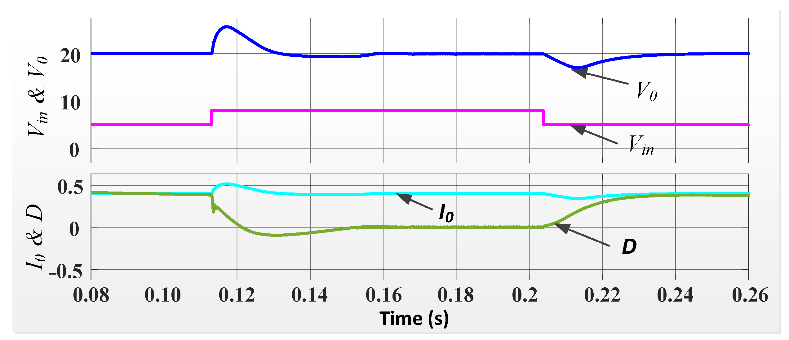
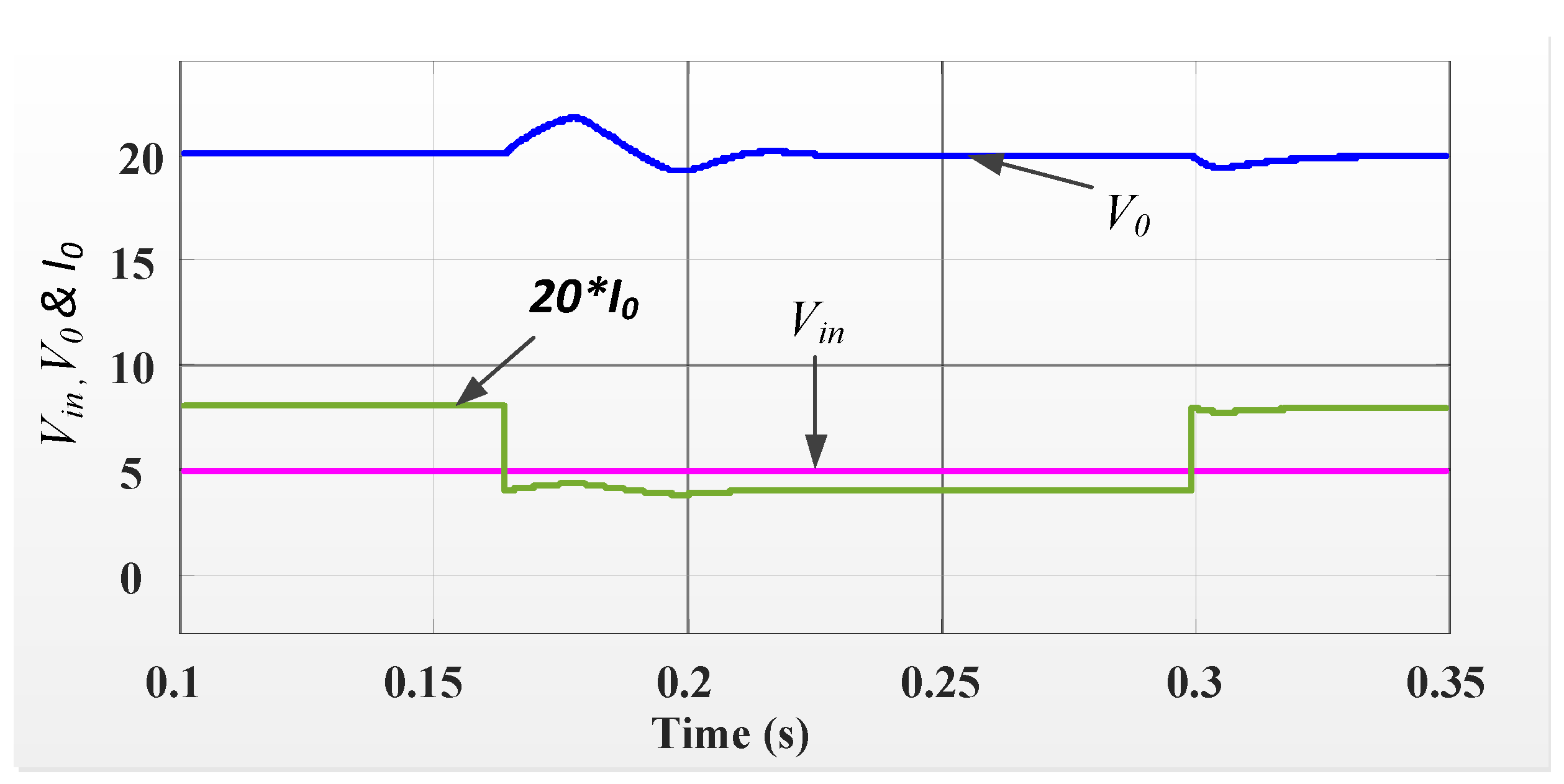
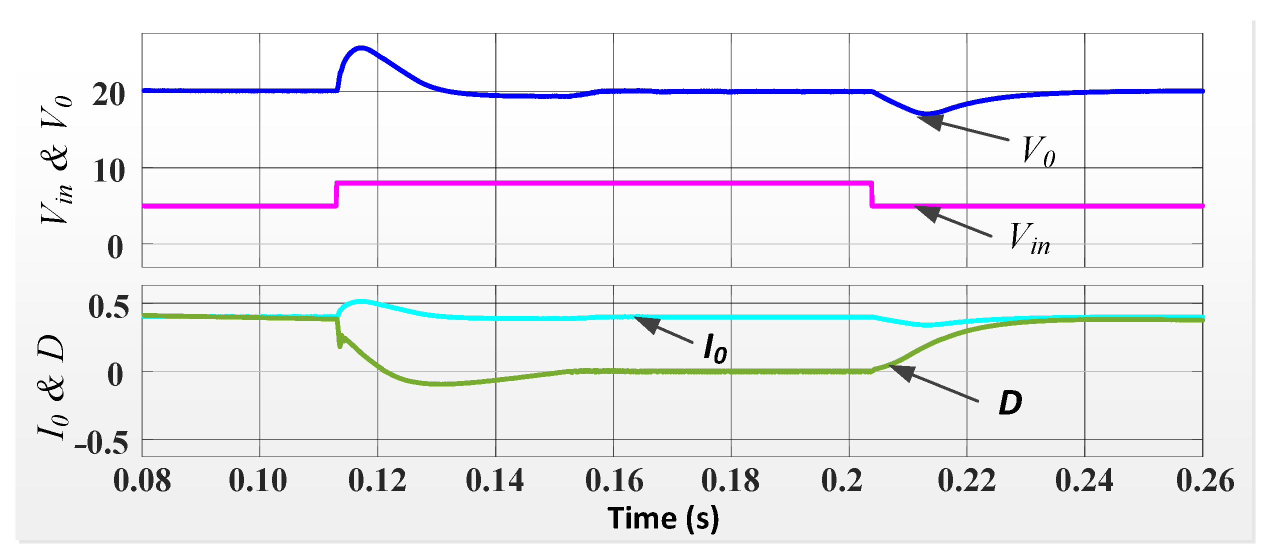
The responses obtained using simulation for varying input are presented in Figure 8. In this case, the reference voltage is set to 20 V and a 100 load resistor is used. Two steps are taken to vary the input voltage. Initially, it is settled at 5 V, then it is changed to 8 V and back to 5 V at certain instants of time as shown in Figure 8. The output response displayed by Figure 8 may be used to assess how the controller can swiftly and effectively regulate the output while suppressing disturbances such as sudden fluctuations in input voltage. ADRC uses the ESO to identify the variations in the states of the converter due to the fluctuations in input voltage. After that, it uses error feedback to dynamically modify the duty cycle in order to keep the output voltage steady. Even when input voltage fluctuates unpredictably, this method guarantees strong, adaptive control.
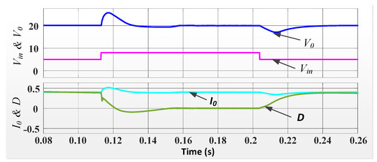
Figure 8.
Response of the output voltage to varying input.
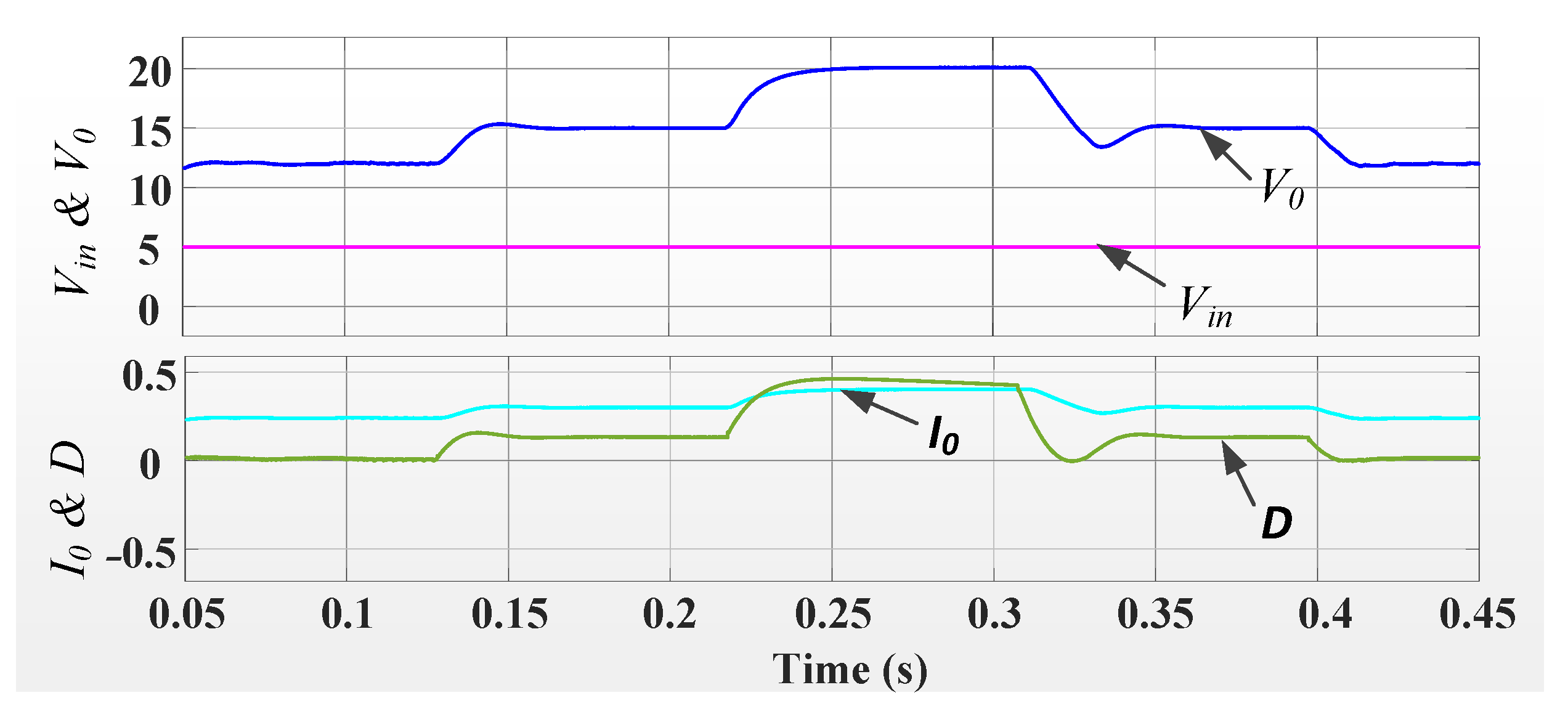
Furthermore, the load resistance is varied while the setpoint and the input voltages remain fixed at 20 V and 5 V, respectively. A 50 load resistor is utilized initially but, after a short while, it is abruptly changed to 100 and then back to 50 . Figure 9 displays the responses under this load variation. Since the load current is lower, the response of the current is multiplied by 20 and plotted thereafter for improved visibility, which explains the variation in the load. The output voltage settles to the reference voltage right away and has a very small ripple magnitude. The resulting response demonstrates decisively the controlled system’s capacity to reject disturbances under various load conditions. The variables like output voltage and inductor current are continually monitored by the ESO. These parameters are changed by an abrupt change in load, and the ESO records this as a disturbance in its state estimations. After that, the state error feedback produces a duty cycle according to the disturbance estimates and error. Hence, it provides a robustness against the varying loads.
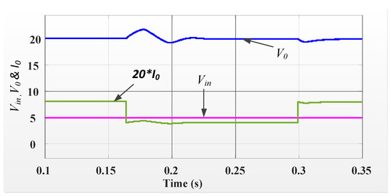
Figure 9.
Response of the output voltage to varying load.
6.2. Hardware Results
The complete experimental setup is depicted in Figure 10. A 200 watt prototype is developed for the proposed circuit. In the experimental setup, MOSFET-IXFH80N65X2 designed by IXYS company from Milpitas, CA, USA and Diode-SL80F040 manufactured by SL Power Electronics, a company based in the Calabasas, CA, USA were used. A gate driver circuit is used to feed the control signal to the MOSFET’s gate terminal.
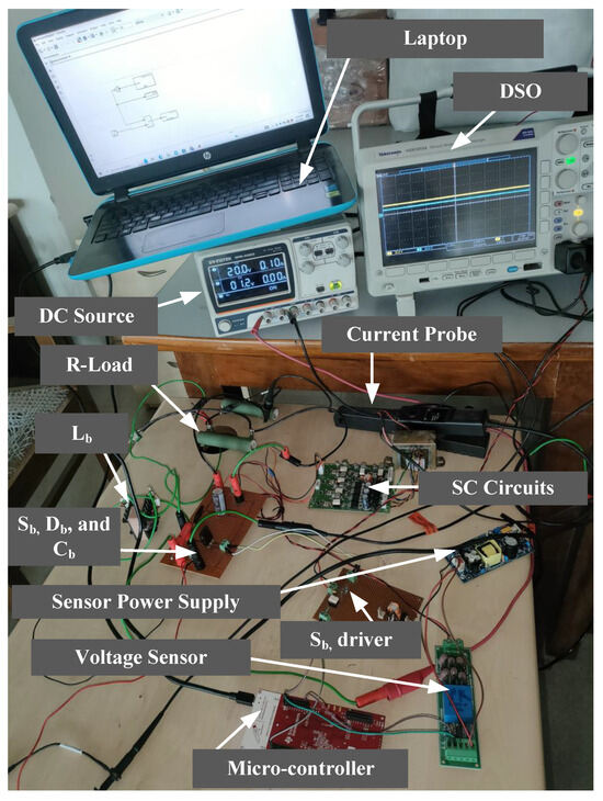
Figure 10.
Experimental prototype.
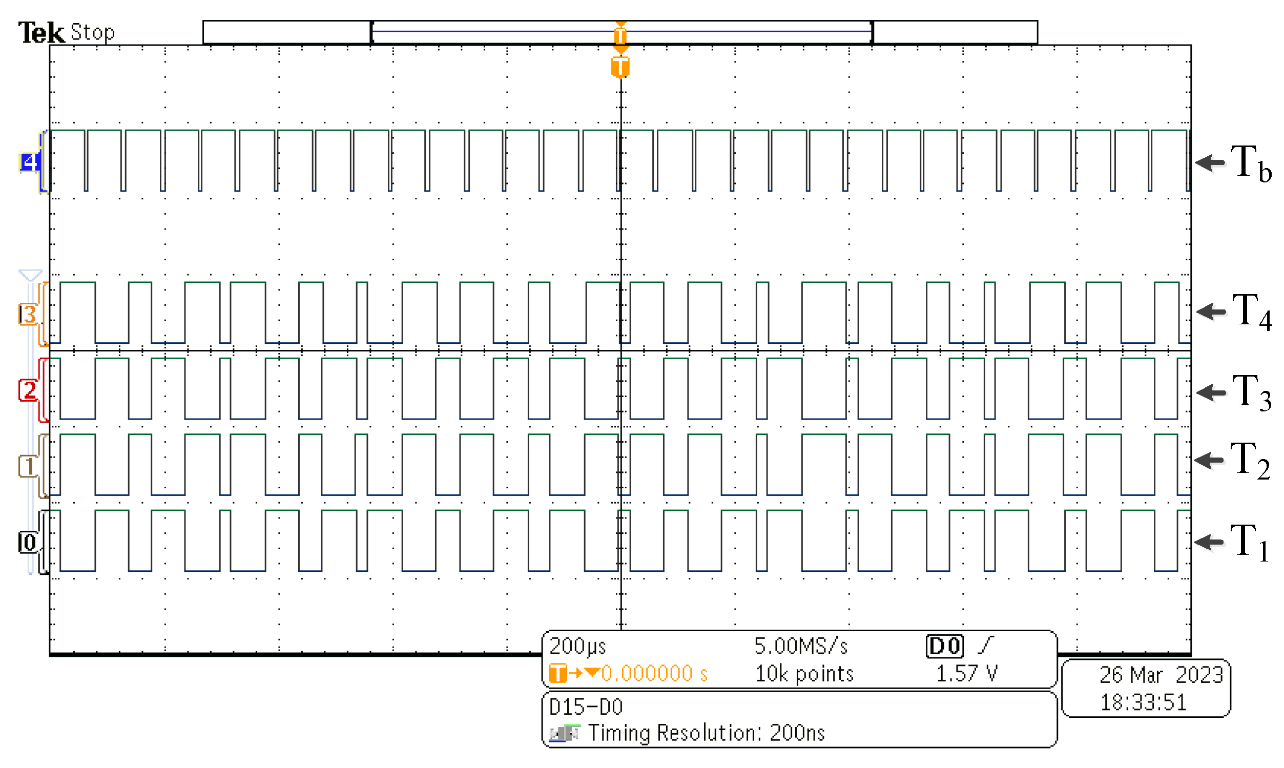
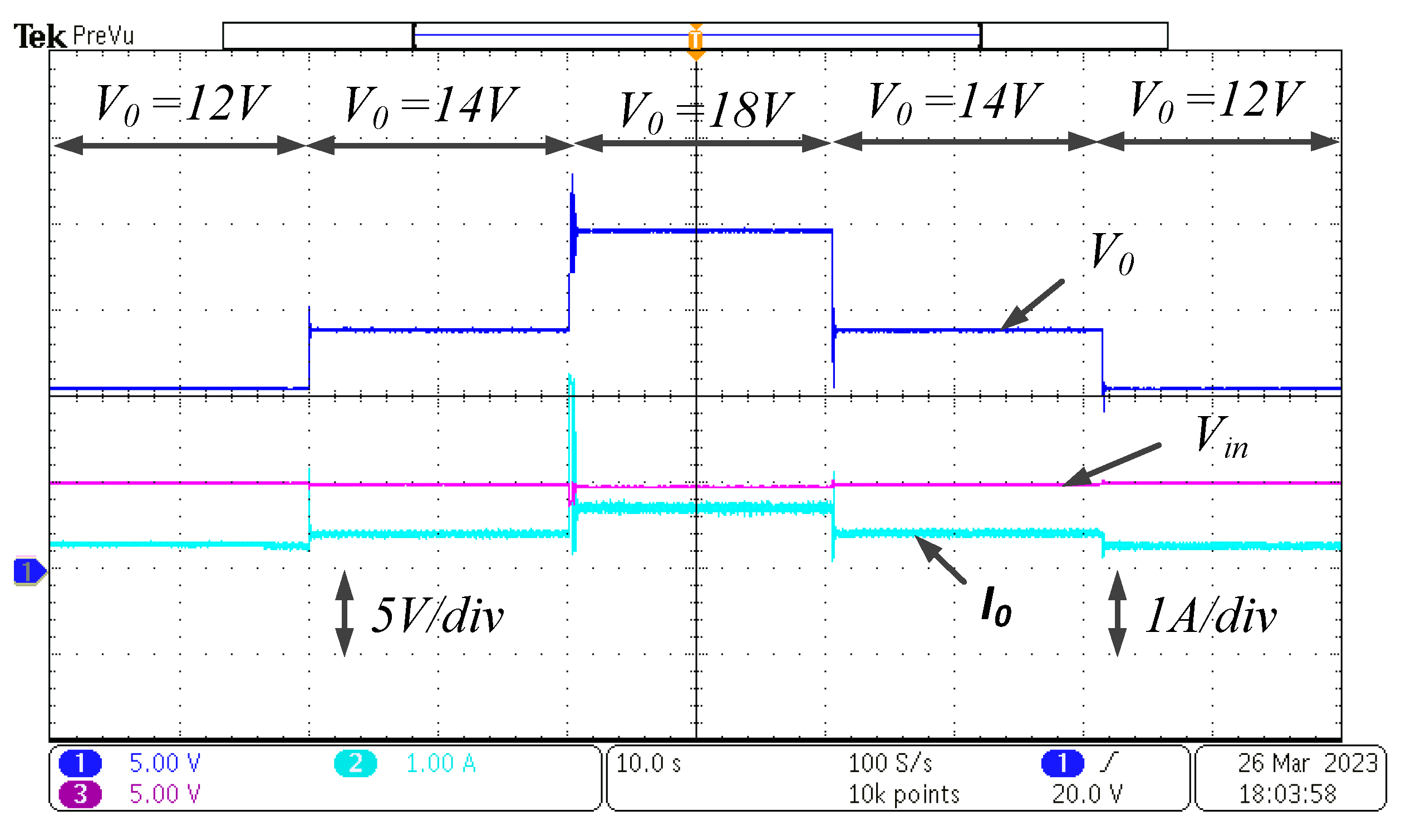
The gate driver circuit enhances the PWM pulse generated by microcontroller TMS320F 28379D designed by Texas Instruments (TI), a company based in the Dallas, TX, USA is programmed by the MATLAB code composer studio. The gate pulse fed to various MOSFETs is shown in Figure 11. Here, the numbers ‘0’ to ‘4’ beside the pulses represents the switching pulses for the switches , , , and respectively as labelled in the Figure 11. An LV-55P voltage sensor developed and manufactured by LEM (Liaisons Electroniques et Mécaniques), a company based in Pfäffikon, Switzerland is used to sense the output voltage and feed it to the microcontroller that ultimately supplies the controller feedback structure. An APCSMP09 source designed by APC Instruments, a company based in India is used for supplying ±15 V to the sensor. A programmable DC source is used as the input voltage to the circuit. The waveforms are recorded on a multiport DSO with the help of current and voltage probes. To verify the servo performance of the system, the reference is varied similarly to that in the simulation and the response obtained is depicted in Figure 12. From the figure, it is determined that the system has a good reference tracking ability and the experimental and simulation results match satisfactorily.
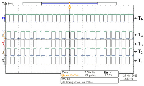
Figure 11.
Gate pulses for different switches.
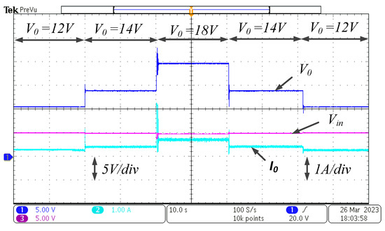
Figure 12.
Responses obtained for variation in reference.
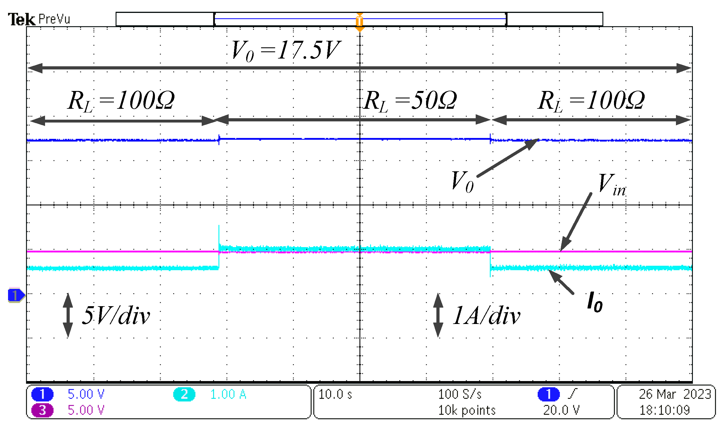
Disturbance rejection abilities can be inferred from Figure 13 and Figure 14. This shows that the effect of disturbance owing to load and input voltage variations on the output voltage is suppressed immediately by the controller. The load variations are performed by varying the resistance from 100 to 50 to 100 , keeping the reference and input voltages at 20 V and 5 V, respectively. The output voltage remains constant in spite of variations in the load. However, the load affects the load current. Similarly, no effect is seen on the output voltage when the input voltage is varied from 5 V to 8 V to 5 V, keeping the reference at 20 V and load at 100 .
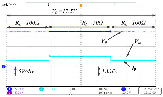
Figure 13.
Responses obtained for variation in load.
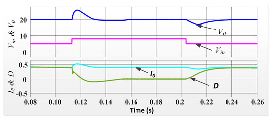
Figure 14.
Responses obtained for variation in input.
7. Loss Analysis for the Proposed Converter
Using the model that the author developed in [33], the detailed loss calculations are performed by taking into account the losses occurring in the switches (switching () + conduction losses ()) and diodes (conduction losses ()). These losses are computed for ON-state voltage drops and energy factors with the help of quadratic curves. A curve-fitting tool is used for obtaining these curves with the help of datasheets of the switches and diodes. In this work, the datasheet of MOSFET IXFH80N65X2 is used for the respective calculations. The corresponding Equations (47)–(51) are given as follows:
Here, and are the ON-state voltage drops of the MOSFET and diode, respectively. is the current through the switch and is the current through the diode. and are the energy factors of the MOSFET in the ON and OFF states, respectively. The OFF-state energy factor for the diode is denoted by . Equations (47)–(51) are used to calculate the losses according to the procedure explained in [33,34,35]. From Equation (52), the efficiency for the developed converter may be obtained as follows:
where and are the output and input powers of the converter, respectively. The calculated losses and efficiencies are summarized in Table 3. The table summarizes the losses of each switch and diode calculated during four different rated power outputs and the efficiencies are calculated accordingly. From the table, it can be seen that maximum efficiency is obtained at 96.6% when the rated power is 111 watts. The experimental efficiencies are also calculated for the proposed circuit and it is found to be lower than the theoretical efficiency. The full load experimental efficiency for the proposed circuit is calculated to be 94.07%. The efficiency value decreases both above and below the full load.
Table 3.
An evaluation of the proposed converter’s efficiency.
8. Conclusions
The presented converter makes use of a switched-capacitor network to meet the requirement of a significantly high-voltage gain for renewable energy applications. The switches are operated with two individual duty ratios, providing a very-high-voltage gain. The availability of two duty ratios makes it easier for the user to attain large gains without utilizing a single duty ratio at higher values. The variations in the voltage gain with respect to duty cycles are demonstrated graphically. In the proposed converter, the voltage stress on the switches is lower as compared to those obtained in [22,23]. Both switching and conduction losses are taken into account for calculating the converter’s efficiency. The efficiency of the designed converter for various loads is found to be above 95%. The closed-loop control strategy utilizing the ADRC controller is implemented on the proposed converter by selecting the controller’s and observer’s bandwidths as 900 rad/s and 3600 rad/s, respectively. Both simulation and experimental outcomes validate that the newly developed converter along with the ADRC control attains an elevated voltage gain, effective load regulation, and rapid transient response that make the converter suitable for microgrid applications. Other advanced control techniques such as sliding mode control, adaptive control, model predictive control, etc. may be implemented on the newly constructed converter.
Author Contributions
Conceptualization, P.K. and A.K.S. (Ashutosh Kumar Singh); methodology, P.K.; software, P.K. and A.K.S. (Ashutosh Kumar Singh); validation, P.K. and A.K.S. (Ashutosh Kumar Singh); formal analysis, P.K.; investigation, P.K.; resources, P.K. and A.K.S. (Ashutosh Kumar Singh); data curation, P.K.; writing—original draft preparation, P.K.; writing—review and editing, P.K. and M.A.; visualization, P.K.; supervision, M.A. and R.K.M.; project administration, P.K., A.K.S. (Ashutosh Kumar Singh) and M.A.; funding acquisition, A.K.S. (Akshay Kumar Saha). All authors have read and agreed to the published version of the manuscript.
Funding
This research received no external funding.
Data Availability Statement
The original contributions presented in the study are included in the article; further inquiries can be directed to the corresponding author.
Conflicts of Interest
The authors declare no conflicts of interest.
References
- Kebede, A.A.; Kalogiannis, T.; Van Mierlo, J.; Berecibar, M. A comprehensive review of stationary energy storage devices for large scale renewable energy sources grid integration. Renew. Sustain. Energy Rev. 2022, 159, 112213. [Google Scholar] [CrossRef]
- Appelbaum, J.; Peled, A.; Aronescu, A. Wall Shading Losses of Photovoltaic Systems. Energies 2024, 17, 5089. [Google Scholar] [CrossRef]
- Luo, F.L.; Ye, H. Advanced dc/dc Converters; CRC Press: Boca Raton, FL, USA, 2016. [Google Scholar]
- Dahale, S.; Das, A.; Pindoriya, N.M.; Rajendran, S. An overview of DC-DC converter topologies and controls in DC microgrid. In Proceedings of the 2017 7th International Conference on Power Systems (ICPS), Shivajinagar, India, 21–23 December 2017; pp. 410–415. [Google Scholar]
- Zhao, Q.; Lee, F.C. High-efficiency, high step-up DC-DC converters. IEEE Trans. Power Electron. 2003, 18, 65–73. [Google Scholar] [CrossRef]
- Hwu, K.; Peng, T. A novel buck–boost converter combining KY and buck converters. IEEE Trans. Power Electron. 2011, 27, 2236–2241. [Google Scholar] [CrossRef]
- Smedley, K.M.; Cuk, S. Dynamics of one-cycle controlled Cuk converters. IEEE Trans. Power Electron. 1995, 10, 634–639. [Google Scholar] [CrossRef]
- Luo, F.L.; Ye, H. Super-lift boost converters. IET Power Electron. 2014, 7, 1655–1664. [Google Scholar] [CrossRef]
- Zhang, J.; Huang, X.; Wu, X.; Qian, Z. A high efficiency flyback converter with new active clamp technique. IEEE Trans. Power Electron. 2010, 25, 1775–1785. [Google Scholar] [CrossRef]
- Lakshmi, M.; Hemamalini, S. Nonisolated high gain DC–DC converter for DC microgrids. IEEE Trans. Ind. Electron. 2017, 65, 1205–1212. [Google Scholar] [CrossRef]
- Yang, L.S.; Liang, T.J. Analysis and implementation of a novel bidirectional DC–DC converter. IEEE Trans. Ind. Electron. 2011, 59, 422–434. [Google Scholar] [CrossRef]
- Maksimovic, D.; Cuk, S. Switching converters with wide DC conversion range. IEEE Trans. Power Electron. 1991, 6, 151–157. [Google Scholar] [CrossRef]
- Loera-Palomo, R.; Morales-Saldaña, J.A. Family of quadratic step-up dc–dc converters based on non-cascading structures. IET Power Electron. 2015, 8, 793–801. [Google Scholar] [CrossRef]
- Wijeratne, D.S.; Moschopoulos, G. Quadratic power conversion for power electronics: Principles and circuits. IEEE Trans. Circuits Syst. Regul. Pap. 2011, 59, 426–438. [Google Scholar] [CrossRef]
- Singh, A.K.; Raushan, R.; Mandal, R.K.; Ahmad, M.W. A New Single-Source Nine-Level Quadruple Boost Inverter (NQBI) for PV Application. IEEE Access 2022, 10, 36246–36253. [Google Scholar] [CrossRef]
- Tran, V.T.; Nguyen, M.K.; Choi, Y.O.; Cho, G.B. Switched-capacitor-based high boost DC-DC converter. Energies 2018, 11, 987. [Google Scholar] [CrossRef]
- Nguyen, M.K.; Duong, T.D.; Lim, Y.C. Switched-capacitor-based dual-switch high-boost DC–DC converter. IEEE Trans. Power Electron. 2017, 33, 4181–4189. [Google Scholar] [CrossRef]
- Chen, S.J.; Yang, S.P.; Huang, C.M.; Chou, H.M.; Shen, M.J. Interleaved high step-up DC-DC converter based on voltage multiplier cell and voltage-stacking techniques for renewable energy applications. Energies 2018, 11, 1632. [Google Scholar] [CrossRef]
- Folmer, S.; Stala, R. DC-DC high voltage gain switched capacitor converter with multilevel output voltage and zero-voltage switching. IEEE Access 2021, 9, 129692–129705. [Google Scholar] [CrossRef]
- Kumar, M.; Yadav, V.K.; Verma, A.K. Switched capacitor based high gain boost converter for renewable energy application. IEEE J. Emerg. Sel. Top. Ind. Electron. 2023, 4, 818–826. [Google Scholar] [CrossRef]
- Janabi, A.; Wang, B. Switched-capacitor voltage boost converter for electric and hybrid electric vehicle drives. IEEE Trans. Power Electron. 2019, 35, 5615–5624. [Google Scholar] [CrossRef]
- Abutbul, O.; Gherlitz, A.; Berkovich, Y.; Ioinovici, A. Step-up switching-mode converter with high voltage gain using a switched-capacitor circuit. IEEE Trans. Circuits Syst. Fundam. Theory Appl. 2003, 50, 1098–1102. [Google Scholar] [CrossRef]
- Rodič, M.; Milanovič, M.; Truntič, M.; Ošlaj, B. Switched-Capacitor boost converter for low power energy harvesting applications. Energies 2018, 11, 3156. [Google Scholar] [CrossRef]
- Kumar, P.; Ajmeri, M.; Singh, A.K.; Mandal, R.K. Novel high-gain boost converter with experimentally validated ADRC control technique for renewable energy applications. Electr. Eng. 2024, 1–10. [Google Scholar] [CrossRef]
- Zhou, R.; Fu, C.; Tan, W. Implementation of linear controllers via active disturbance rejection control structure. IEEE Trans. Ind. Electron. 2020, 68, 6217–6226. [Google Scholar] [CrossRef]
- Herbst, G. A Simulative Study on Active Disturbance Rejection Control (ADRC) as a Control Tool for Practitioners. Electronics 2013, 2, 246–279. [Google Scholar] [CrossRef]
- Chu, Z.; Wu, C.; Sepehri, N. Active disturbance rejection control applied to high-order systems with parametric uncertainties. Int. J. Control Autom. Syst. 2019, 17, 1483–1493. [Google Scholar] [CrossRef]
- Kumar, P.; Ajmeri, M. Robust control of a single-ended primary inductor converter using adrc technique. Eng. Res. Express 2023, 6, 015010. [Google Scholar] [CrossRef]
- Ahmad, S.; Ali, A. Active disturbance rejection control of DC–DC boost converter: A review with modifications for improved performance. IET Power Electron. 2019, 12, 2095–2107. [Google Scholar] [CrossRef]
- Li, H.; Liu, X.; Lu, J. Research on linear active disturbance rejection control in DC/DC boost converter. Electronics 2019, 8, 1249. [Google Scholar] [CrossRef]
- Gao, Z. Scaling and bandwidth-parameterization based controller tuning. In Proceedings of the Atlantic Coast Conference, Tallahassee, FL, USA, 13–16 March 2003; pp. 4989–4996. [Google Scholar]
- Gao, Z. Active disturbance rejection control: A paradigm shift in feedback control system design. In Proceedings of the 2006 American Control Conference, Minneapolis, MN, USA, 14–16 June 2006; p. 7. [Google Scholar]
- Ali, A.I.M.; Sayed, M.A.; Takeshita, T. Isolated single-phase single-stage DC-AC cascaded transformer-based multilevel inverter for stand-alone and grid-tied applications. Int. J. Electr. Power Energy Syst. 2021, 125, 106534. [Google Scholar] [CrossRef]
- Singh, A.K.; Mandal, R.K. A Novel 17-Level Reduced Component Single DC Switched-Capacitor-Based Inverter with Reduced Input Spike Current. IEEE J. Emerg. Sel. Top. Power Electron. 2022, 10, 6045–6056. [Google Scholar] [CrossRef]
- Singh, A.K.; Mandal, R.K.; Anand, R. Quasi-Resonant Switched-Capacitor-Based Seven-Level Inverter with Reduced Capacitor Spike Current. IEEE J. Emerg. Sel. Top. Power Electron. 2023, 11, 1953–1965. [Google Scholar] [CrossRef]


Disclaimer/Publisher’s Note: The statements, opinions and data contained in all publications are solely those of the individual author(s) and contributor(s) and not of MDPI and/or the editor(s). MDPI and/or the editor(s) disclaim responsibility for any injury to people or property resulting from any ideas, methods, instructions or products referred to in the content. |
© 2024 by the authors. Licensee MDPI, Basel, Switzerland. This article is an open access article distributed under the terms and conditions of the Creative Commons Attribution (CC BY) license (https://creativecommons.org/licenses/by/4.0/).