

Advanced Single-Phase PLL-Based Transfer Delay Operators: A Comprehensive Review and Optimal Loop Filter Design


Abstract
1. Introduction
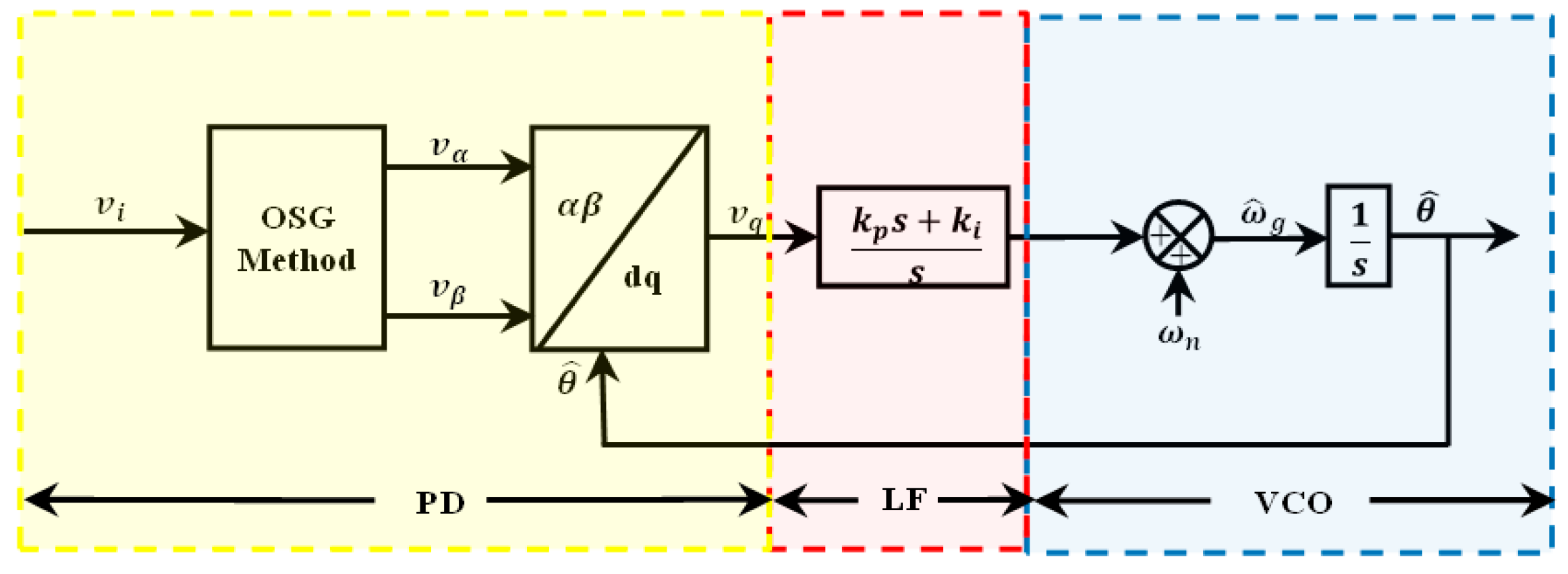
2. Transfer Delay PLLs
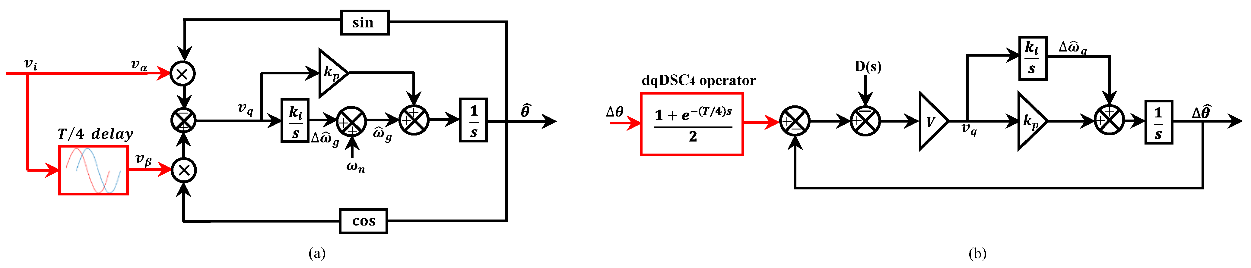
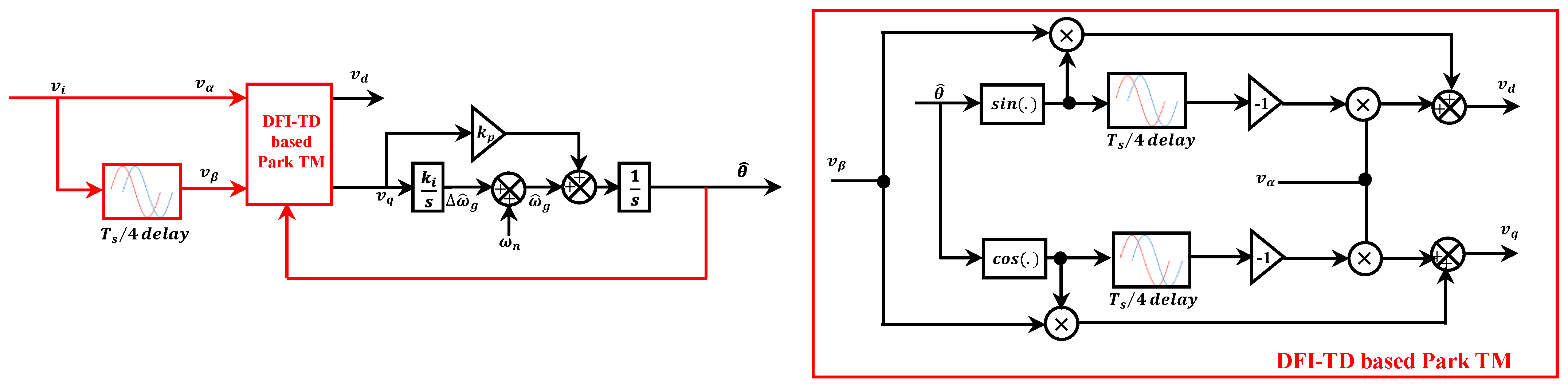
2.1. Standard TD-PLL
2.2. Non-Frequency Dependent TD-PLL (NTD-PLL)
2.3. Enhanced Time Delay PLL (ETD-PLL)
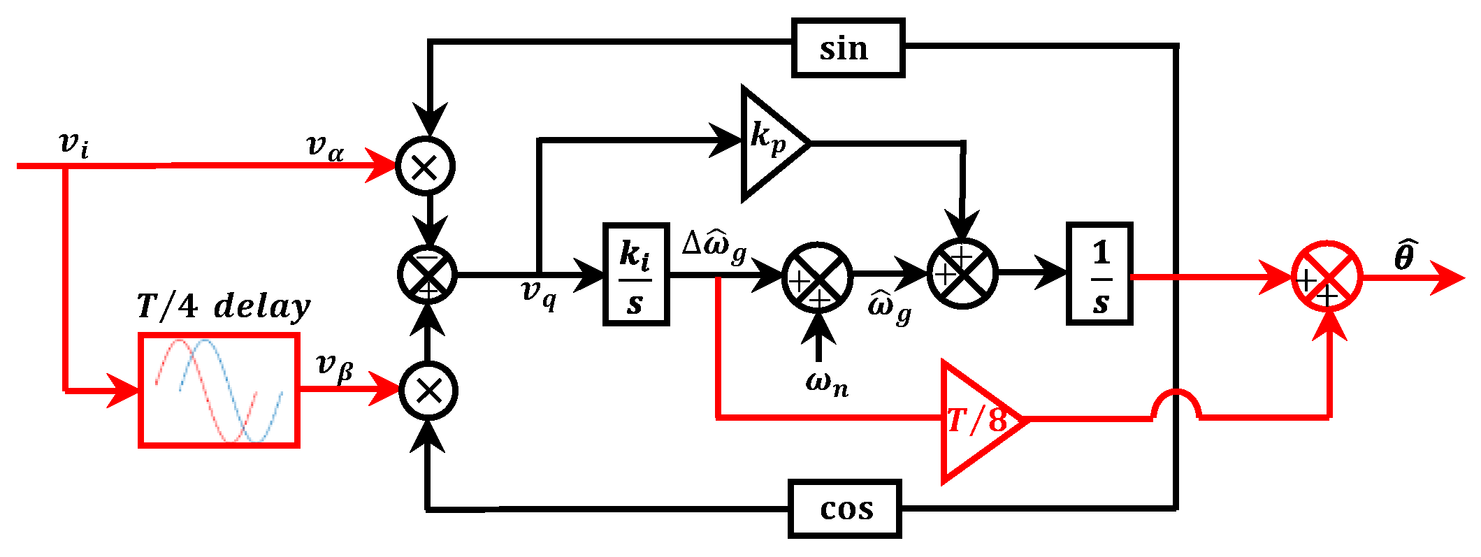
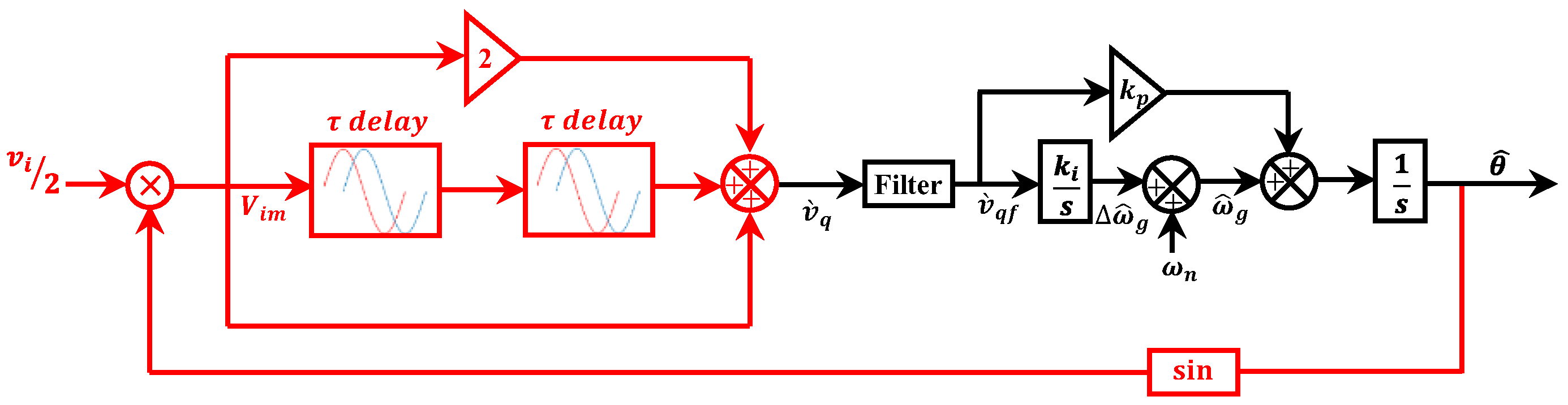
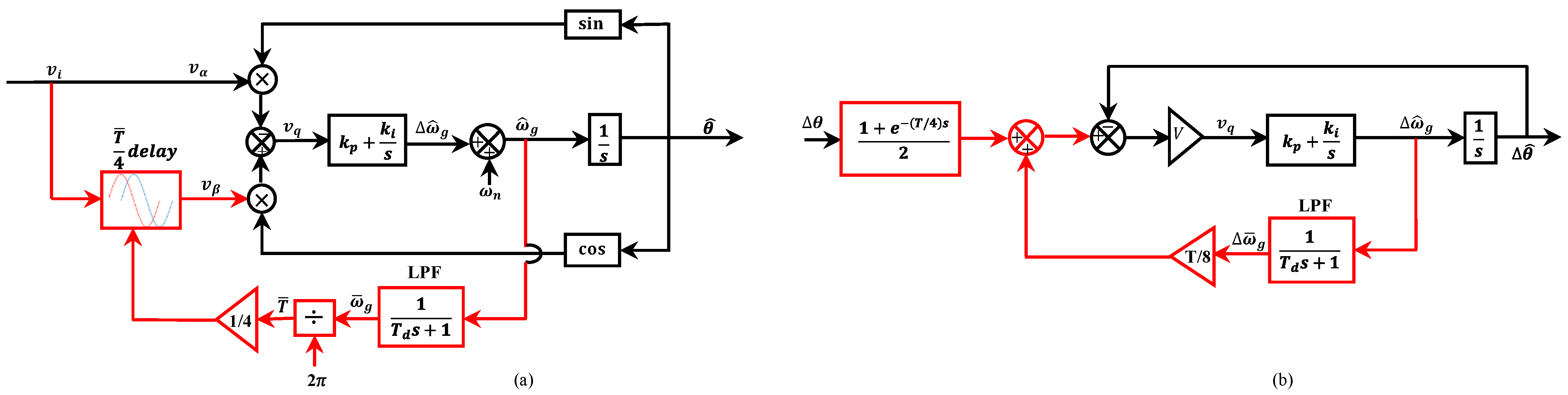
2.4. Adaptive Time Delay PLL (ATD-PLL)
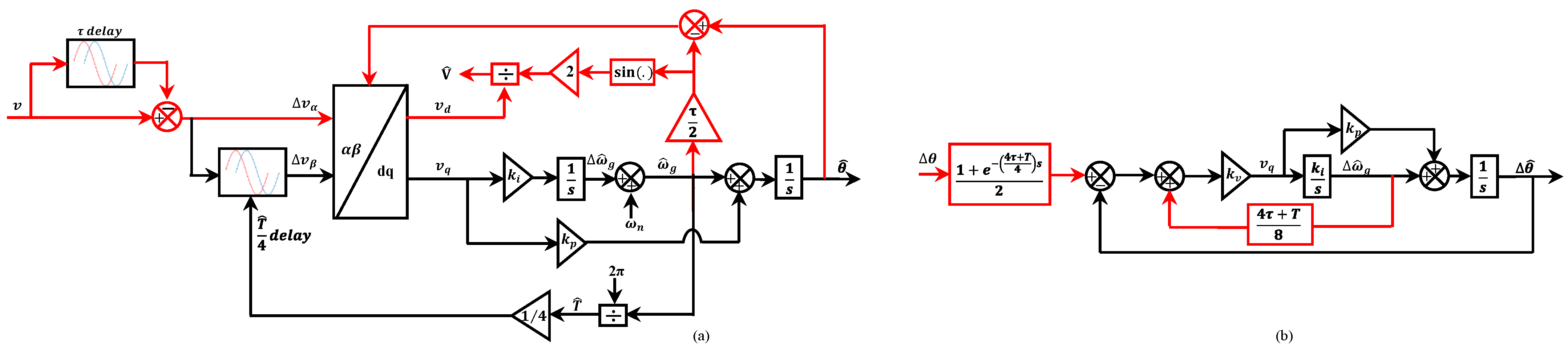
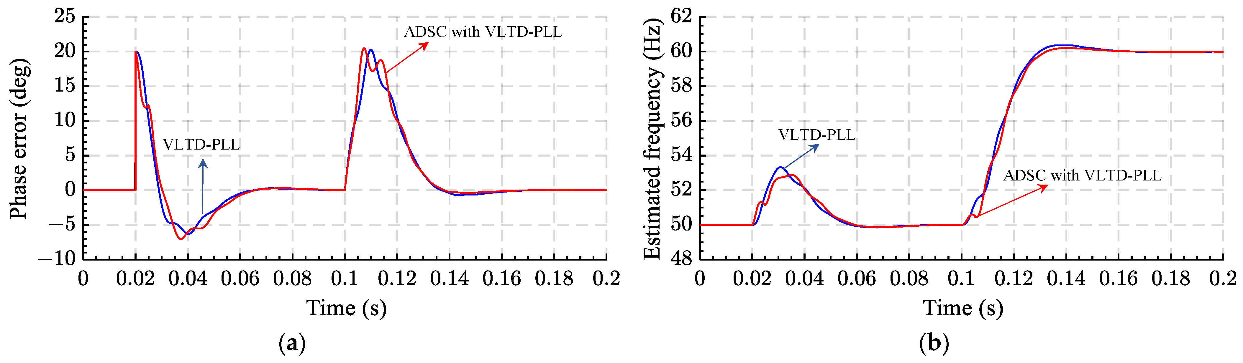
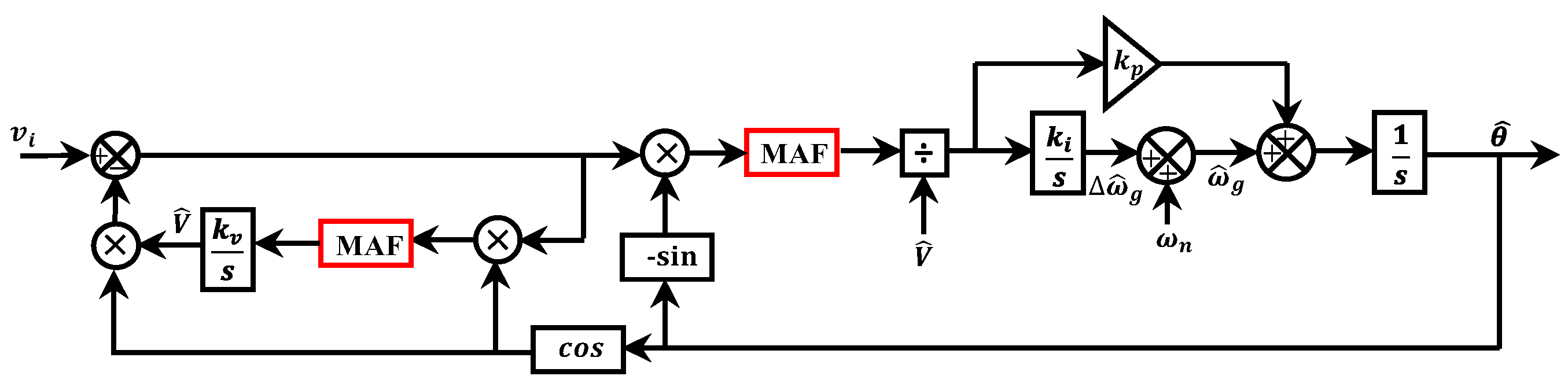
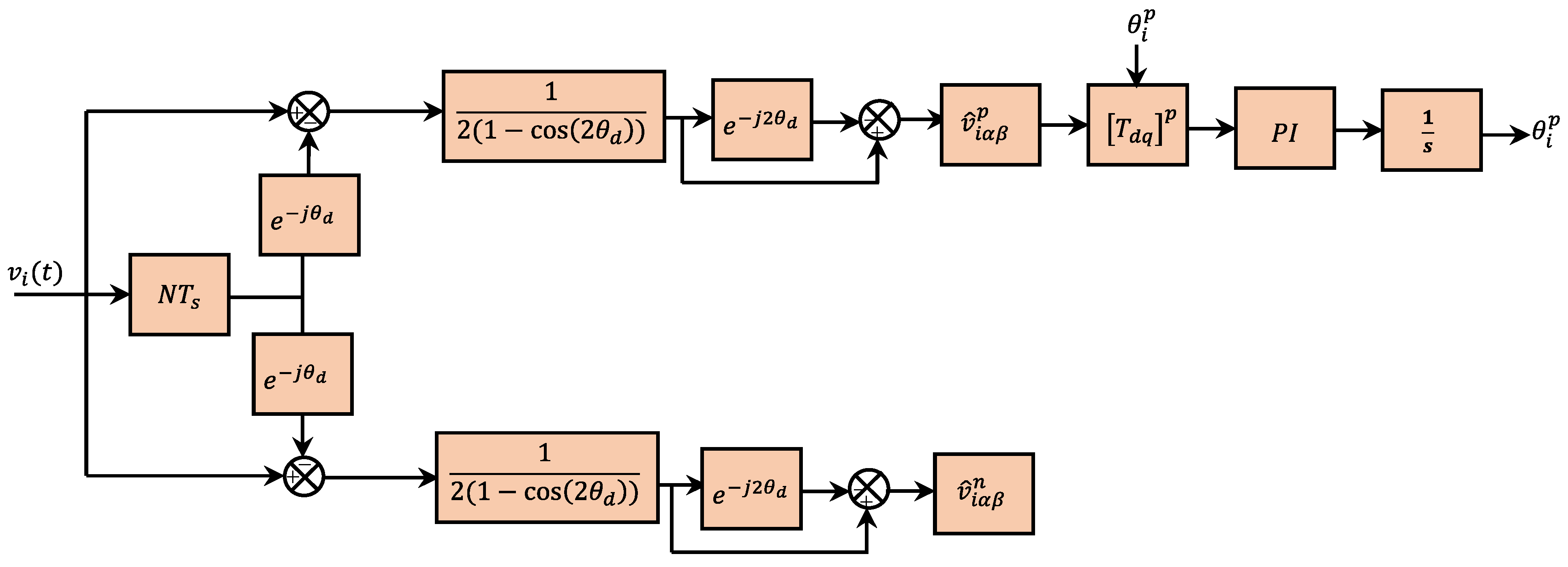
2.5. Variable Length Time Delay PLL (VLTD-PLL)
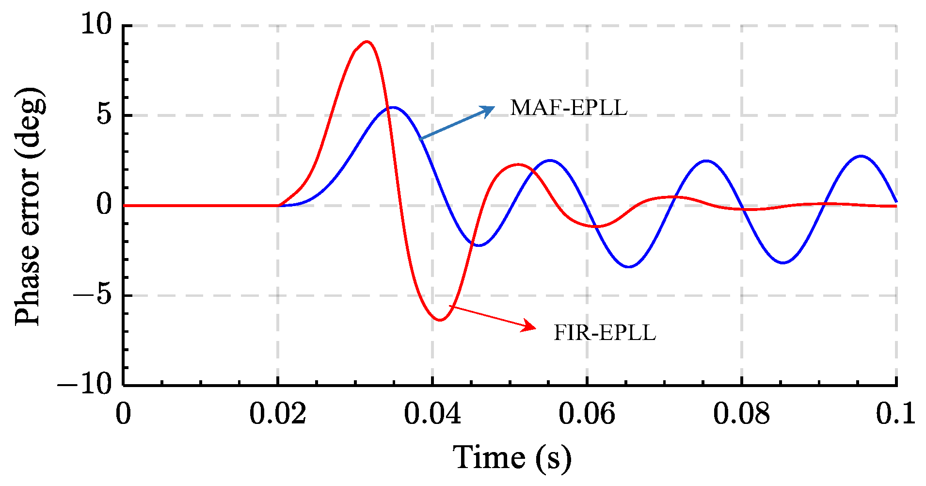
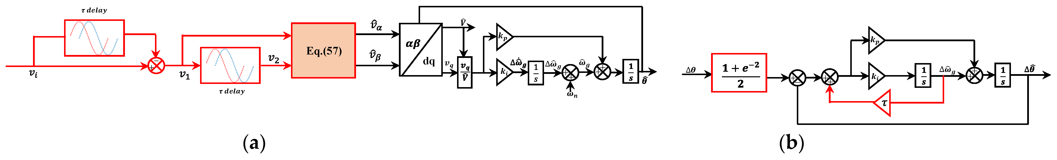
2.6. Enhanced PLL-Based Moving Average Filter or a Finite Impulse Response Filter
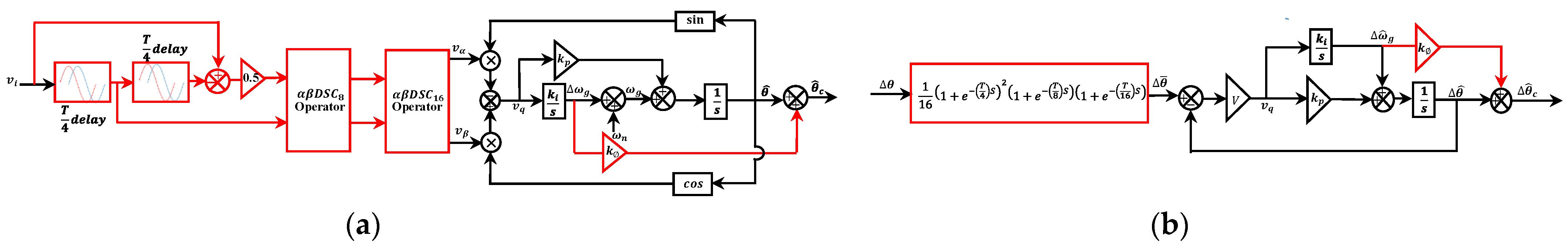
2.7. Advanced 1- DSC-PLLs
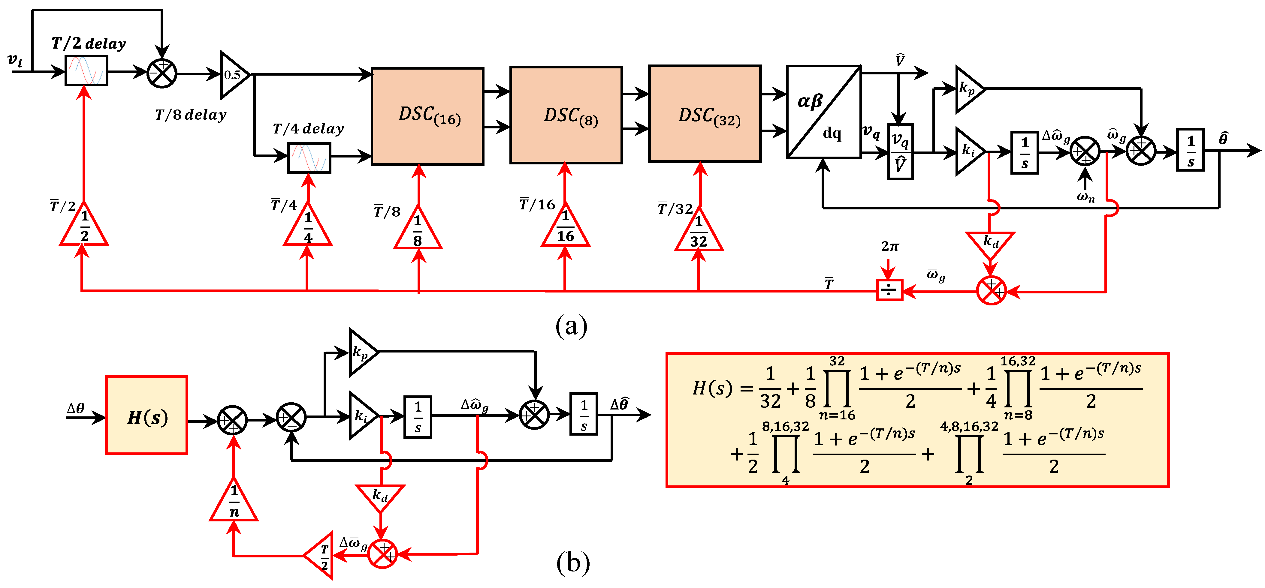
2.7.1. Adaptive 1- CDSC-PLL
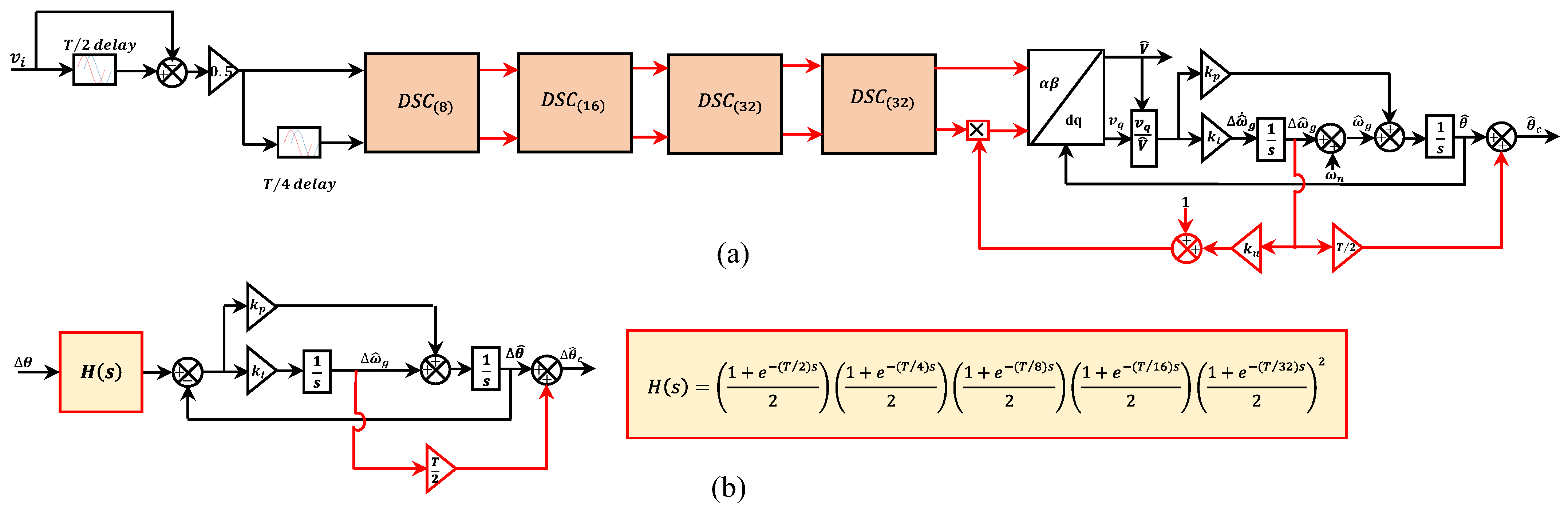
2.7.2. Non-Adaptive 1- CDSC-PLL1
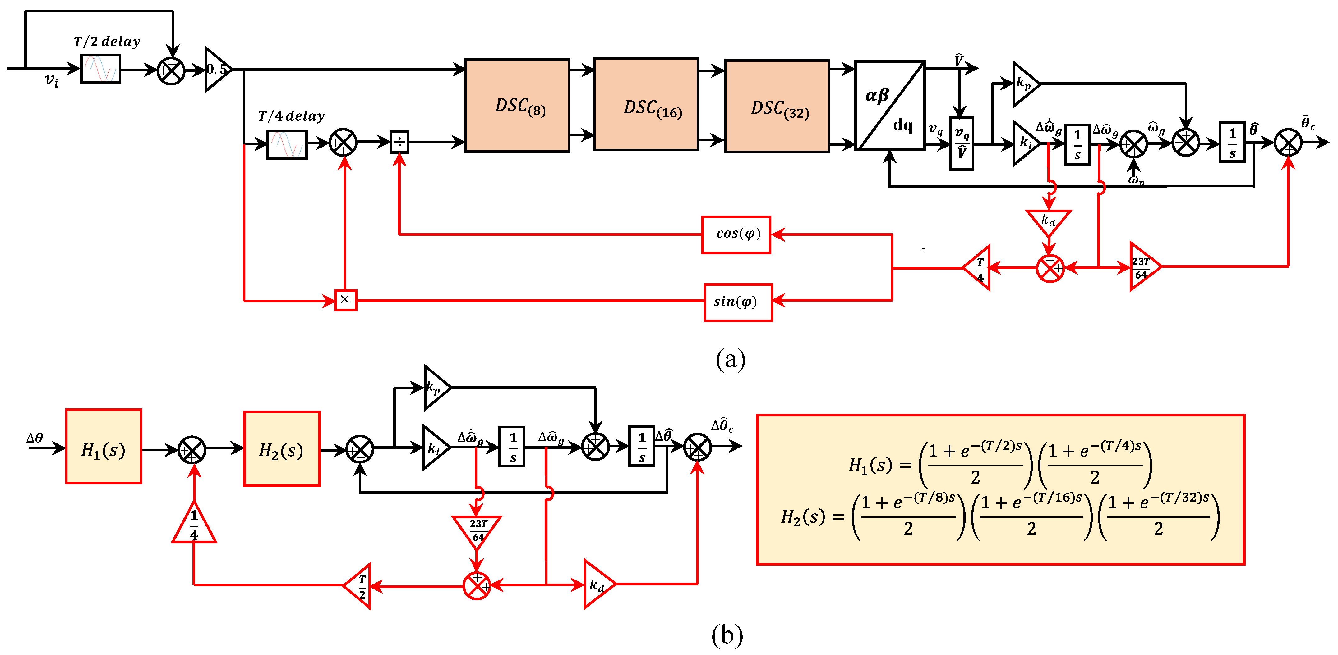
2.7.3. Non-Adaptive 1- CDSC-PLL2
2.8. Fast Delayed Signal Cancellation-Based PLL (FDSC-PLL)
2.9. Two Sample PLL (2S-PLL)
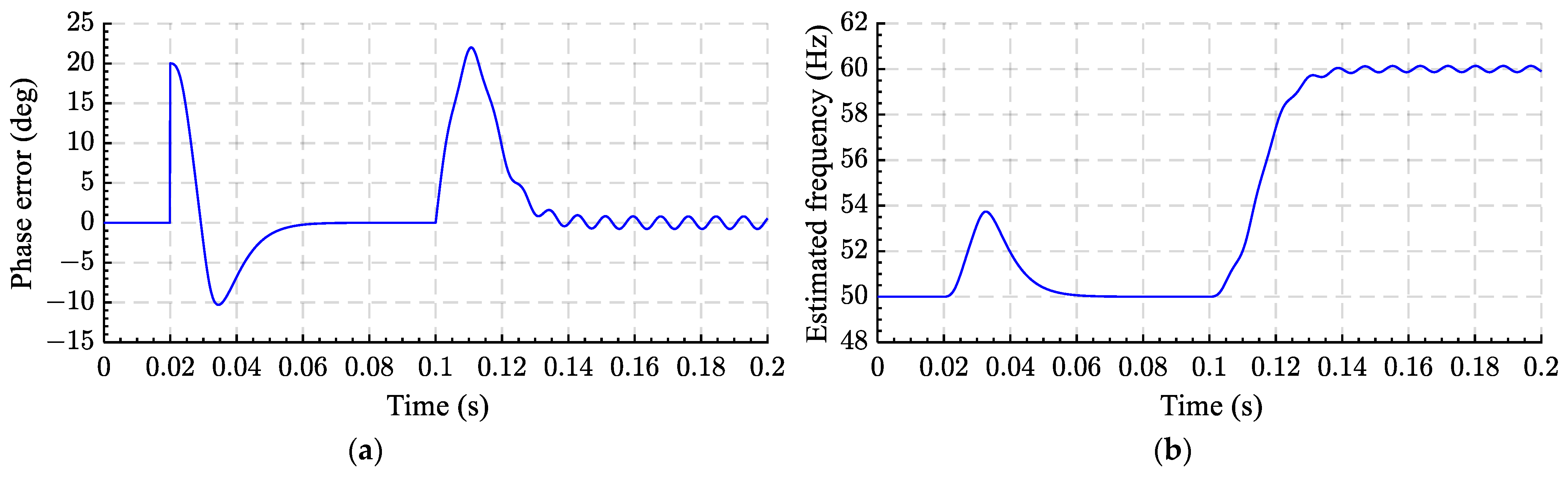
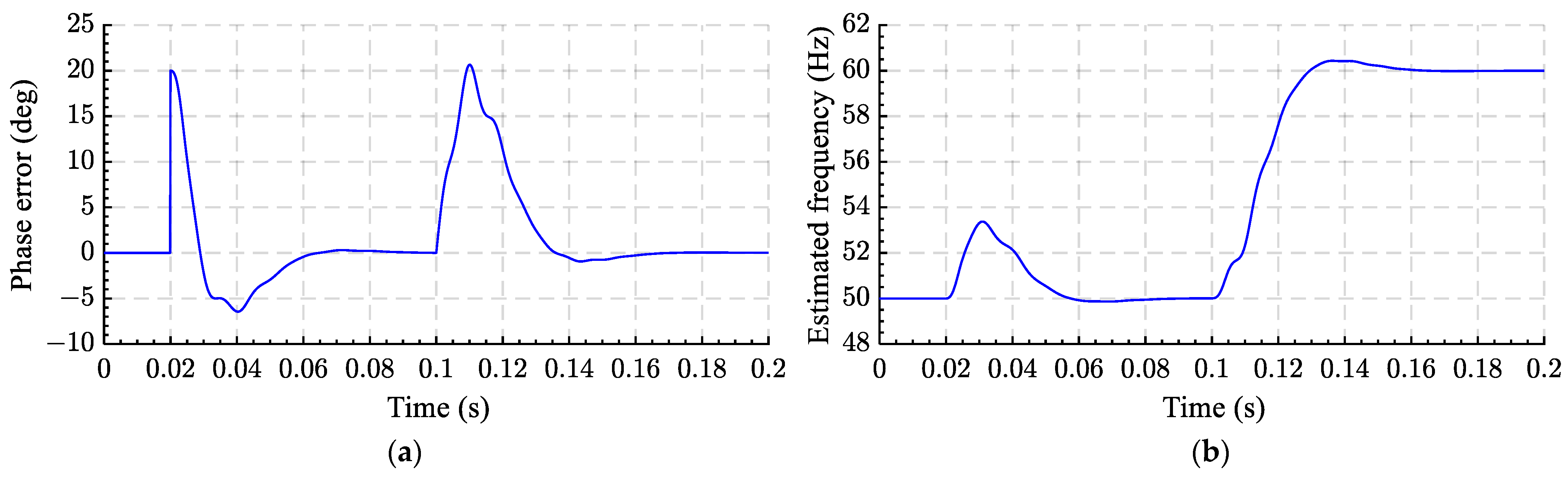
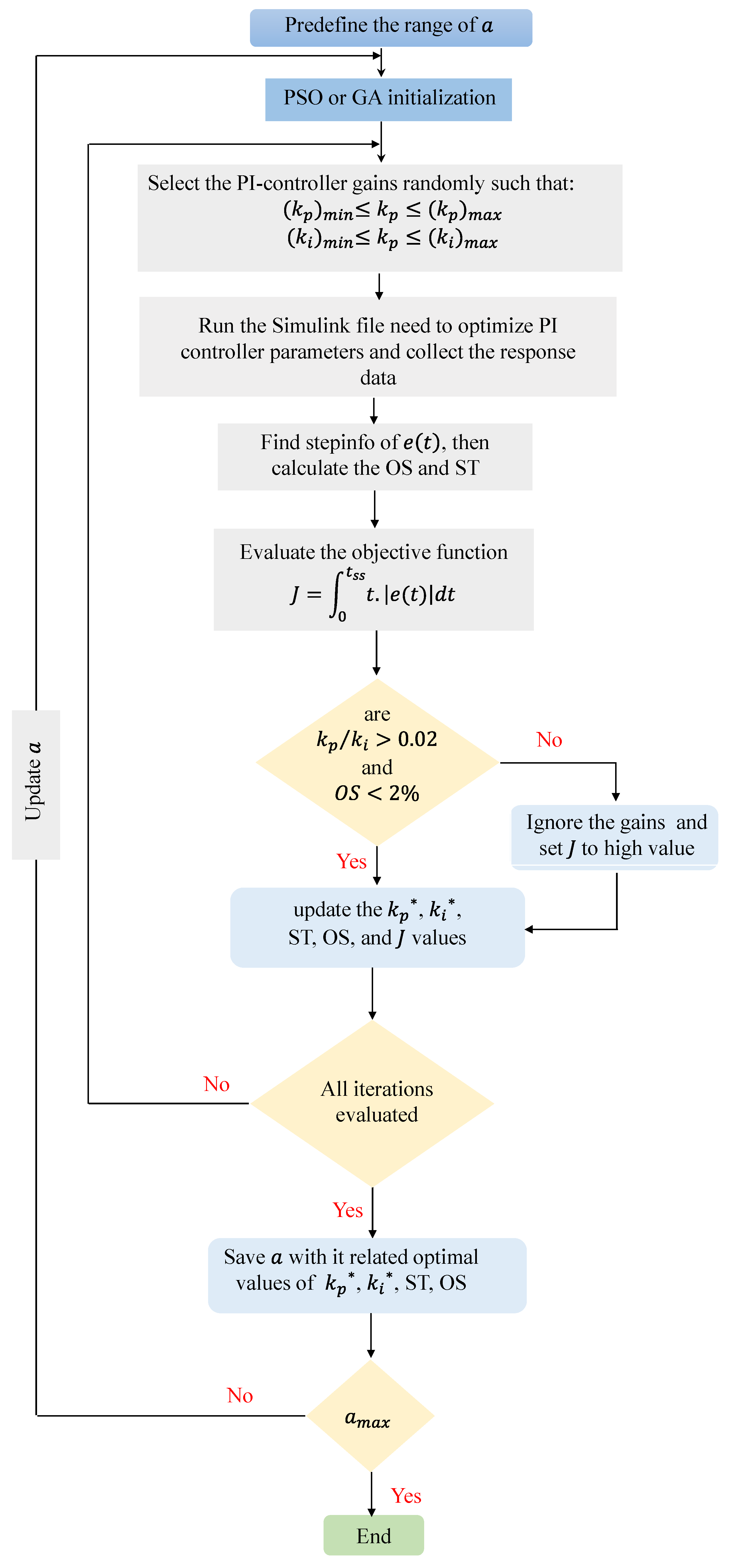
3. Optimal Loop Filter (LF) Design Based on a Large-Signal Model
4. Discussion
- The conventional TD-PLL requires a phase compensator to achieve a zero average phase error under the frequency variation. However, the harmonics filtering is poor and cannot reject the DC offset.
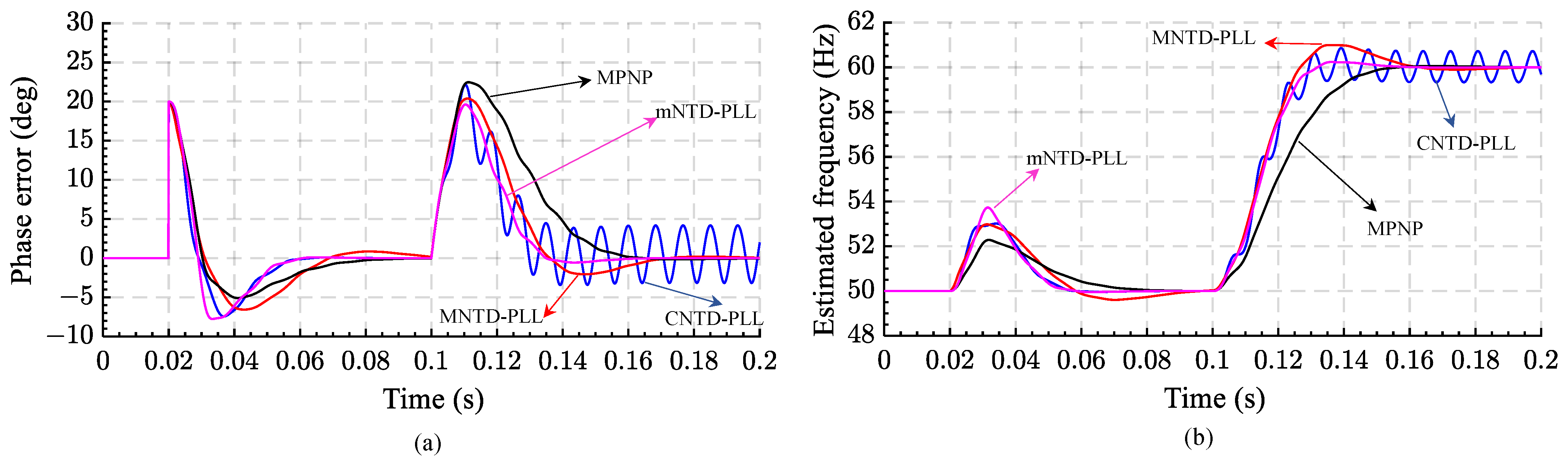
- The CNTD-PLL structure has a five-modified version, including an MNTD-PLL, MNP, MPNP, mNTD-PLL, and tNTD-PLL. The double frequency oscillatory error under the frequency drafts is eliminated from all except the CNTD-PLL and mNTD-PLL, which still suffer from it in frequency and amplitude responses, respectively. The harmonics filtering and DC offset rejection are poor for all except MNP and MPNP. However, all disturbances are mitigated using MNP and MPNP depending on the selected MAF window length, resulting in a slow dynamic performance and high memory requirements.
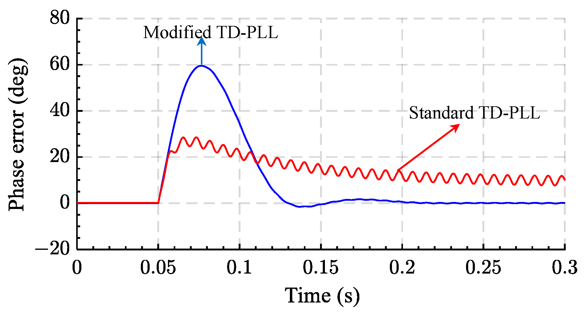
- The ETD-PLL, ATD-PLL, VLTD-PLL, and ADSC-based VLTD-PLL perfectly removed the double frequency oscillatory error under the frequency draft. However, only ADSC-based VLTD-PLLs can reject the DC offset perfectly. The ATD-PLL has a minimum memory requirement compared with this group of PLLs.
- All of the MAF-EPLLs, FIR-EPLLs, and modified FIR-EPLLs have good harmonic filtering. However, MAF-EPLLs cannot reject DC offset unless the window length is the same as the fundamental grid period.
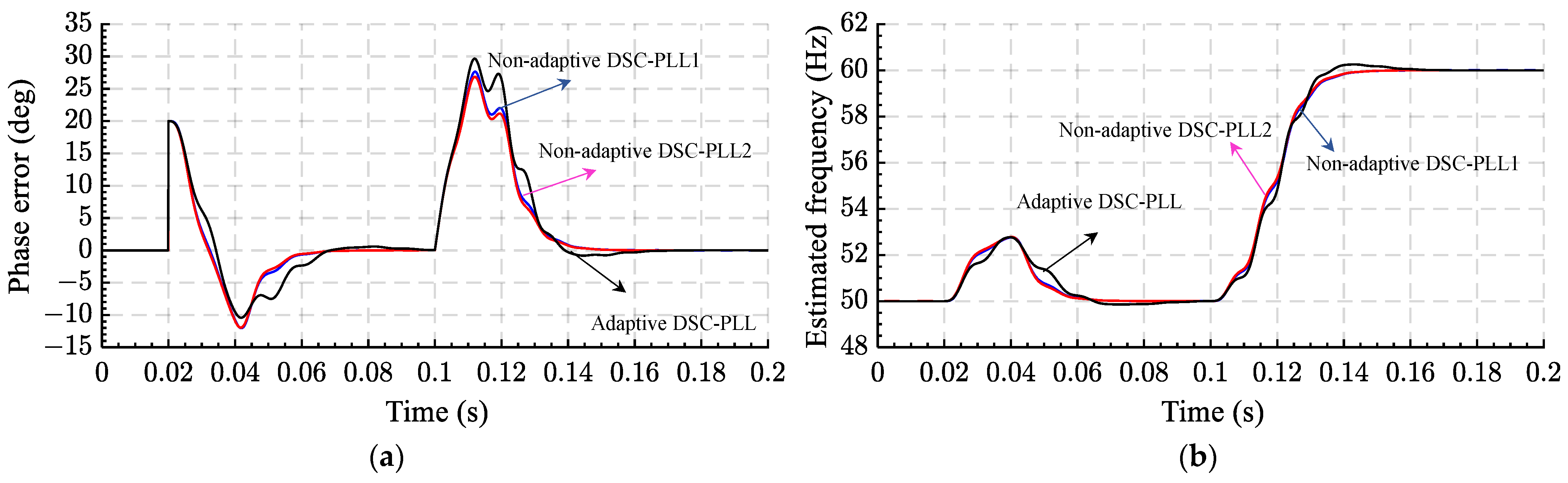
- Good harmonics filtering and the perfect DC offset rejection are achieved using adaptive and non-adaptive DSC-PLLs. However, the use of adaptation operators increased the design complexity.
- It is well known that the estimated amplitude is a by-product of the PLL. In the nominal frequency case, the d-axis output of the Park transformation estimates the grid voltage. However, amplitude correction must be applied to the estimated d-axis component using frequency-fixed DC offset rejection to estimate the amplitude correctly. The correction factor can be obtained from the transfer function of the PLL.
5. Conclusions
Author Contributions
Funding
Conflicts of Interest
Abbreviations
| ATD-PLL | Adaptive TD-PLL |
| ADSC | Arbitrarily Delayed Signal Cancellation |
| CE | Characteristic Equation |
| CDSC | Cascaded Delayed Signal Cancellation |
| CNTD-PLL | Conventional NTD-PLL |
| DFOE | Double Frequency Oscillatory Error |
| DSP | Digital Signal Processing |
| ETD-PLL | Enhanced TD-PLL |
| FDSC-PLL | Fast DSC-PLL |
| FIR-EPLL | A Finite Impulse Filter |
| IAE | The Integral Absolute Error |
| ISE | The Integral Square Error |
| ITAE | The Integral Time Absolute Error |
| GA | Genetic Algorithm |
| LSM | Large-Signal Model |
| LTI | Linear Time-Invariant |
| LTP | Linear Time-Periodic Framework |
| LF | Loop Filtering |
| LQR | Linear Quadratic Regulator |
| MAF | Moving Average Filter |
| MNTD-PLL | Modified NTD-PLL |
| MPNP | MAF PLC NTD-PLL |
| MDNTD-PLL | Modified Digital NTD-PLL |
| MSNPLL | Modified Standard NTD-PLL |
| NTD-PLL | Non-Frequency Dependant TD-PLL |
| OS | Overshoot |
| PI | Proportional-Integral |
| PD | Phase Detector |
| PM | The Phase Margin |
| PLC | Phase Lead Compensator |
| PLL | Phase-Locked Loop |
| pPLL | Power Based PLL |
| PSO | Particle Swarm Optimization |
| QSG | Quadrature Signal Generation |
| ST | Settling Time |
| SSM | Small-Signal Model |
| SO | Symmetrical Optimum |
| SRF | Synchronous Reference Frame |
| 2S-PLL | Two Sample-Based PLL |
| TD | Time Delay |
| tNTD-PLL | A Truly NTD-PLL |
| TM | Transformation Matrix |
| VCO | Voltage Controlled Oscillator |
| VLTD-PLL | Variable Length TD-PLL |
| List of symbols | |
| 1- | Single phase |
| The constant that determines the phase margin | |
| , | Terms decaying to zero at time constant equal |
| The deviation of the grid frequency from its nominal value | |
| The deviation in estimated grid frequency | |
| The deviation in the estimated phase | |
| The deviation in the grid voltage phase | |
| Positive parameter selected to be equal to 1 | |
| The phase error compensator of the ETD-PLL | |
| The amplitude scaling factor | |
| The proportional gain of the PI controller | |
| The optimal proportional gain of the PI controller based optimization algorithm; GA and PSO | |
| The integral gain of the PI controller | |
| The optimal integral gain of the PI controller based optimization algorithm; GA and PSO | |
| The filtered version of the estimated grid period of the VLTD-PLL | |
| The delay length of mNTD-PLL | |
| Half of the selected time delay | |
| The ratio between the proportional gain over the integral gain | |
| The window period of MAF | |
| τ | The delay length of the ADSC |
| Grid voltage phase | |
| The estimated phase | |
| A constant value equal to | |
| The initial phase | |
| V | The grid amplitude |
| The estimated grid amplitude | |
| N | The number of samples in the DSP memory |
| and | The time-domain αβ -signals |
| vi | The grid voltage |
| The PI controller input signal | |
| ωn | The nominal grid frequency |
| The cut-off frequency of lowpass filter | |
| The actual grid frequency | |
| The estimated frequency | |
| ωN | The natural damping |
| The crossover frequency | |
| The desired damping ratio |
Appendix A

| TD-PLLs Types | PI-Controller Parameters | Tuning Method | ||
|---|---|---|---|---|
|
Standard TD-PLL | Second order characteristic | = | ||
| CNTD-PLL | Symmetric optimum method | = | ||
| MNTD-PLL | , | Symmetric optimum method | = | |
| MPNP | Symmetric optimum method | = | ||
| mNTD-PLL | ---------------------------- | ---------------------------- | = | |
| ETD-PLL | Second order characteristic | = | ||
| ATD-PLL | Second order characteristic | = | ||
| VLTD-PLL | Second order characteristic | = | ||
| ADSC with VLTD-PLL | Second order characteristic | = | ||
| mFIR-EPLL | , | Second order characteristic | = | |
| Adaptive CDSC-PLL | Second order characteristic | = | ||
|
Non-adaptive DSC-PLL1 | Second order characteristic | = | ||
|
Non-adaptive DSC-PLL2 | Second order characteristic | = |
Appendix B
| Tuning Method | Parameters | Range |
|---|---|---|
| Second order characteristic | (0.5–1) (2) [rad/s] | |
| Symmetric optimum method | (1.732–3.732) |
References
- Karimi-Ghartemani, M. Linear and pseudolinear enhanced phased-locked loop (EPLL) structures. IEEE Trans. Ind. Electron. 2013, 61, 1464–1474. [Google Scholar] [CrossRef]
- Karimi-Ghartemani, M.; Karimi, H.; Khajehoddin, S.A.; Hoseinizadeh, S.M. Efficient modeling systematic design of enhanced phase-locked loop structures. IEEE Trans. Power Electron. 2022, 37, 9061–9072. [Google Scholar] [CrossRef]
- Xia, T.; Zhang, X.; Tan, G.; Liu, Y. All-pass-filter-based PLL for single-phase grid-connected converters under distorted grid conditions. IEEE Access 2020, 8, 106226–106233. [Google Scholar] [CrossRef]
- Smadi, I.A.; Albatran, S.; Ahmad, H.J.J.E. On the performance optimization of two-level three-phase grid-feeding voltage-source inverters. Energies 2018, 11, 400. [Google Scholar] [CrossRef]
- Albatran, S.; Smadi, I.A.; Ahmad, H.J.; Koran, A.J.E. Online optimal switching frequency selection for grid-connected voltage source inverters. Electronics 2017, 6, 110. [Google Scholar] [CrossRef]
- Giotopoulos, V.; Korres, G.J.E. Implementation of Phasor Measurement Unit Based on Phase-Locked Loop Techniques: A Comprehensive Review. Energies 2023, 16, 5465. [Google Scholar] [CrossRef]
- Silwal, S.; Karimi-Ghartemani, M.; Karimi, H.; Davari, M.; Zadeh, S.M.H. A multivariable controller in synchronous frame integrating phase-locked loop to enhance performance of three-phase grid-connected inverters in weak grids. IEEE Trans. Power Electron. 2022, 37, 10348–10359. [Google Scholar] [CrossRef]
- Dash, A.; Muduli, U.R.; Al Jaafari, K.; Al Hosani, K.; Iqbal, A.; Behera, R.K. Harmonic mitigation and dc offset rejection for grid-tied dstatcom with cesogi-wpf control. In Proceedings of the 2022 3rd International Conference on Smart Grid and Renewable Energy (SGRE), Doha, Qatar, 20–22 March 2022; pp. 1–6. [Google Scholar]
- Li, Y.; Wang, D.; Ning, Y.; Hui, N. DC-offset elimination method for grid synchronisation. Electron. Lett. 2017, 53, 335–337. [Google Scholar] [CrossRef]
- Karimi-Ghartemani, M.; Khajehoddin, S.A.; Jain, P.K.; Bakhshai, A.; Mojiri, M. Addressing DC component in PLL and notch filter algorithms. IEEE Trans. Power Electron. 2011, 27, 78–86. [Google Scholar] [CrossRef]
- Smadi, I.A.; Atawi, I.E.; Ibrahim, A.A. An Improved Delayed Signal Cancelation for Three-Phase Grid Synchronization with DC Offset Immunity. Energies 2023, 16, 2873. [Google Scholar] [CrossRef]
- Liu, B.; An, M.; Wang, H.; Chen, Y.; Zhang, Z.; Xu, C.; Song, S.; Lv, Z. A simple approach to reject DC offset for single-phase synchronous reference frame PLL in grid-tied converters. IEEE Access 2020, 8, 112297–112308. [Google Scholar] [CrossRef]
- Xie, M.; Wen, H.; Zhu, C.; Yang, Y. DC offset rejection improvement in single-phase SOGI-PLL algorithms: Methods review and experimental evaluation. IEEE Access 2017, 5, 12810–12819. [Google Scholar] [CrossRef]
- Ardalan, P.; Rasekh, N.; Khaneghah, M.Z.; Abrishamifar, A.; Saeidi, M. A modified SOGI-FLL algorithm with DC-offset rejection improvement for single-phase inverter applications. Int. J. Dyn. Control 2022, 10, 2020–2033. [Google Scholar] [CrossRef]
- Golestan, S.; Guerrero, J.M.; Vasquez, J.C. DC-offset rejection in phase-locked loops: A novel approach. IEEE Trans. Ind. Electron. 2016, 63, 4942–4946. [Google Scholar]
- Ahmed, H.; Benbouzid, M. Demodulation type single-phase PLL with DC offset rejection. Electron. Lett. 2020, 56, 344–347. [Google Scholar] [CrossRef]
- Hoseinizadeh, S.M.; Karimi, H.; Karimi-Ghartemani, M. A Robust Phase-Locked Loop-Integrated Controller in Stationary Frame for Voltage Source Converters Connected to Weak and Unbalanced Grids. IEEE Trans. Ind. Electron. 2023. [Google Scholar] [CrossRef]
- IEC 61727:2004; Characteristics of the Utility Interface for Photovoltaic (PV) Systems. IEC: Geneva, Switzerland, 2004.
- IEEE Std 1547-2003; IEEE Standard for Interconnecting Distributed Resources with the Electric Power System. IEEE: Piscataway, NJ, USA, 2003.
- Arranz-Gimon, A.; Zorita-Lamadrid, A.; Morinigo-Sotelo, D.; Duque-Perez, O. A review of total harmonic distortion factors for the measurement of harmonic and interharmonic pollution in modern power systems. Energies 2021, 14, 6467. [Google Scholar] [CrossRef]
- Khan, S.; Singh, B.; Makhija, P. A review on power quality problems and its improvement techniques. In Proceedings of the 2017 Innovations in Power and Advanced Computing Technologies (i-PACT), Vellore, India, 21–22 April 2017; pp. 1–7. [Google Scholar]
- IEEE Std 519-2014; IEEE Recommended Practice and Requirements for Harmonic Control in Electric Power Systems. IEEE: New York, NY, USA, 2014.
- EN 50160; Voltage Characteristics of Electricity Supplied by Public Distribution Systems. CENELEC: Bruxelles, Belgium, 2010.
- Nejabatkhah, F.; Li, Y.W.; Wu, B. Control strategies of three-phase distributed generation inverters for grid unbalanced voltage compensation. IEEE Trans. Power Electron. 2015, 31, 5228–5241. [Google Scholar]
- Zhang, Y.; Roes, M.; Hendrix, M.; Duarte, J. Symmetric-component decoupled control of grid-connected inverters for voltage unbalance correction and harmonic compensation. Int. J. Electr. Power Energy Syst. 2020, 115, 105490. [Google Scholar] [CrossRef]
- Zhang, P.; Li, L. Vibration and noise characteristics of high-frequency amorphous transformer under sinusoidal and non-sinusoidal voltage excitation. Int. J. Electr. Power Energy Syst. 2020, 123, 106298. [Google Scholar] [CrossRef]
- Yang, D.; Wang, X.; Liu, F.; Xin, K.; Liu, Y.; Blaabjerg, F. Symmetrical PLL for SISO impedance modeling and enhanced stability in weak grids. IEEE Trans. Power Electron. 2019, 35, 1473–1483. [Google Scholar] [CrossRef]
- Xu, J.; Bian, S.; Qian, Q.; Qian, H.; Xie, S. Robustness improvement of single-phase inverters under weak grid cases by adding grid current feedforward in delay-based phase-locked loop. IEEE Access 2020, 8, 124275–124287. [Google Scholar] [CrossRef]
- Hu, B.; Nian, H.; Li, M.; Xu, Y.; Liao, Y.; Yang, J. Impedance-based analysis and stability improvement of DFIG system within PLL bandwidth. IEEE Trans. Ind. Electron. 2021, 69, 5803–5814. [Google Scholar] [CrossRef]
- Xu, J.; Qian, Q.; Zhang, B.; Xie, S. Harmonics and stability analysis of single-phase grid-connected inverters in distributed power generation systems considering phase-locked loop impact. IEEE Trans. Sustain. Energy 2019, 10, 1470–1480. [Google Scholar] [CrossRef]
- Golestan, S.; Guerrero, J.M.; Gharehpetian, G.B. Five approaches to deal with problem of DC offset in phase-locked loop algorithms: Design considerations and performance evaluations. IEEE Trans. Power Electron. 2015, 31, 648–661. [Google Scholar] [CrossRef]
- Smadi, I.A.; Fawaz, B.H.B. DC offset rejection in a frequency-fixed second-order generalized integrator-based phase-locked loop for single-phase grid-connected applications. Prot. Control Mod. Power Syst. 2022, 7, 1–13. [Google Scholar] [CrossRef]
- Sonam, K.; Nikhil, P.; Sudeep, B.; Atul, G. Implementation of single-phase modified SRF-PLL using model based development approach. In Proceedings of the 2017 North American Power Symposium (NAPS), Morgantown, WV, USA, 17–19 September 2017; pp. 1–6. [Google Scholar]
- Golestan, S.; Guerrero, J.M.; Vasquez, J.C. Single-phase PLLs: A review of recent advances. IEEE Trans. Power Electron. 2017, 32, 9013–9030. [Google Scholar] [CrossRef]
- Han, Y.; Luo, M.; Zhao, X.; Guerrero, J.M.; Xu, L. Comparative performance evaluation of orthogonal-signal-generators-based single-phase PLL algorithms—A survey. IEEE Trans. Power Electron. 2015, 31, 3932–3944. [Google Scholar] [CrossRef]
- Iov, F.; Zhao, W.; Kerekes, T.J.E. Robust PLL-Based Grid Synchronization and Frequency Monitoring. Energies 2023, 16, 6856. [Google Scholar] [CrossRef]
- Herrejón-Pintor, G.A.; Melgoza-Vázquez, E.; Monroy-Morales, J.L.J.E. A Three-Phase Synchronization Algorithm Based on a Modified DSOGI with Adjustable Re-Filtering. Energies 2023, 16, 6500. [Google Scholar] [CrossRef]
- Golestan, S.; Matas, J.; Abusorrah, A.M.; Guerrero, J.M. More-stable EPLL. IEEE Trans. Power Electron. 2021, 37, 1003–1011. [Google Scholar] [CrossRef]
- Escobar, G.; Ibarra, L.; Valdez-Resendiz, J.E.; Mayo-Maldonado, J.C.; Guillen, D. Nonlinear stability analysis of the conventional SRF-PLL and enhanced SRF-EPLL. IEEE Access 2021, 9, 59446–59455. [Google Scholar] [CrossRef]
- Sevilmiş, F.; Karaca, H. Efficient implementation and performance improvement of three-phase EPLL under non-ideal grid conditions. IET Power Electron. 2020, 13, 2492–2499. [Google Scholar] [CrossRef]
- Wang, G.; Wu, F. Virtual quadrature-coordinate EPLL for single-phase grid information synchronisation. Electron. Lett. 2019, 55, 109–111. [Google Scholar] [CrossRef]
- Martins, C.H.; Moreira, M.G.; Vale-Cardoso, A.S. A New Approach for EPLL-Based Frequency Estimation under Severe Disturbances. In Proceedings of the 2019 IEEE 10th Annual Information Technology, Electronics and Mobile Communication Conference (IEMCON), Vancouver, BC, Canada, 17–19 October 2019; pp. 0862–0869. [Google Scholar]
- Mohamadian, S.; Pairo, H.; Ghasemian, A. A straightforward quadrature signal generator for single-phase SOGI-PLL with low susceptibility to grid harmonics. IEEE Trans. Ind. Electron. 2021, 69, 6997–7007. [Google Scholar] [CrossRef]
- Prakash, S.; Singh, J.K.; Behera, R.K.; Mondal, A. Comprehensive analysis of SOGI-PLL based algorithms for single-phase system. In Proceedings of the 2019 National Power Electronics Conference (NPEC), Tiruchirappalli, India, 13–15 December 2019; pp. 1–6. [Google Scholar]
- Xu, J.; Qian, H.; Hu, Y.; Bian, S.; Xie, S. Overview of SOGI-based single-phase phase-locked loops for grid synchronization under complex grid conditions. IEEE Access 2021, 9, 39275–39291. [Google Scholar] [CrossRef]
- Kalkoul, S.; Benalla, H.; Nabti, K.; Reama, A. Comparison among single-phase PLLs based on SOGI. In Proceedings of the 2020 6th International Conference on Electric Power and Energy Conversion Systems (EPECS), Istanbul, Turkey, 5–7 October 2020; pp. 118–122. [Google Scholar]
- Lima, F.K.D.A.; Araujo, R.G.; Tofoli, F.L.; Branco, C.G.C. A phase-locked loop algorithm for single-phase systems with inherent disturbance rejection. IEEE Trans. Ind. Electron. 2019, 66, 9260–9267. [Google Scholar] [CrossRef]
- Xiao, F.; Dong, L.; Li, L.; Liao, X. A frequency-fixed SOGI-based PLL for single-phase grid-connected converters. IEEE Trans. Power Electron. 2016, 32, 1713–1719. [Google Scholar] [CrossRef]
- Golestan, S.; Mousazadeh, S.Y.; Guerrero, J.M.; Vasquez, J.C. A critical examination of frequency-fixed second-order generalized integrator-based phase-locked loops. IEEE Trans. Power Electron. 2017, 32, 6666–6672. [Google Scholar] [CrossRef]
- Stojic, D.; Tarczewski, T.; Niewiara, L.J.; Grzesiak, L.M. Improved Fixed-Frequency SOGI Based Single-Phase PLL. Energies 2022, 15, 7297. [Google Scholar] [CrossRef]
- Sahoo, A.; Mahmud, K.; Ravishankar, J. An enhanced frequency-adaptive single-phase grid synchronization technique. IEEE Trans. Instrum. Meas. 2021, 70, 9002611. [Google Scholar] [CrossRef]
- Du, H.; Sun, Q.; Cheng, Q.; Ma, D.; Wang, X. An adaptive frequency phase-locked loop based on a third order generalized integrator. Energies 2019, 12, 309. [Google Scholar] [CrossRef]
- Herrejón-Pintor, G.A.; Melgoza-Vázquez, E.; Chávez, J.D.J. A modified SOGI-PLL with adjustable refiltering for improved stability and reduced response time. Energies 2022, 15, 4253. [Google Scholar] [CrossRef]
- Gude, S.; Chu, C.-C. Single-phase enhanced phase-locked loops based on multiple delayed signal cancellation filters for micro-grid applications. IEEE Trans. Ind. Appl. 2019, 55, 7122–7133. [Google Scholar] [CrossRef]
- Wang, S.; Etemadi, A.; Doroslovački, M. Adaptive cascaded delayed signal cancellation PLL for three-phase grid under unbalanced and distorted condition. Electr. Power Syst. Res. 2020, 180, 106165. [Google Scholar] [CrossRef]
- Ullah, I.; Ashraf, M. Comparison of synchronization techniques under distorted grid conditions. IEEE Access 2019, 7, 101345–101354. [Google Scholar] [CrossRef]
- Sevilmiş, F.; Karaca, H. Implementation of enhanced non-adaptive cascaded DSC-PLLs for renewable energy systems. Int. J. Electr. Power Energy Syst. 2022, 134, 107470. [Google Scholar] [CrossRef]
- Reza, M.S.; Sadeque, F.; Hossain, M.M.; Ghias, A.M.; Agelidis, V.G. Three-phase PLL for grid-connected power converters under both amplitude and phase unbalanced conditions. IEEE Trans. Ind. Electron. 2019, 66, 8881–8891. [Google Scholar] [CrossRef]
- Wu, F.; Li, X. Multiple DSC filter-based three-phase EPLL for nonideal grid synchronization. IEEE J. Emerg. Sel. Top. Power Electron. 2017, 5, 1396–1403. [Google Scholar] [CrossRef]
- Golestan, S.; Guerrero, J.M.; Vasquez, J.C.; Abusorrah, A.M.; Al-Turki, Y. All-pass-filter-based PLL systems: Linear modeling, analysis, and comparative evaluation. IEEE Trans. Power Electron. 2019, 35, 3558–3572. [Google Scholar] [CrossRef]
- Gautam, S.; Xiao, W.; Lu, D.D.-C.; Ahmed, H.; Guerrero, J.M. Development of frequency-fixed all-pass filter-based single-phase phase-locked loop. IEEE J. Emerg. Sel. Top. Power Electron. 2021, 10, 506–517. [Google Scholar] [CrossRef]
- Sevilmiş, F.; Karaca, H. A fast hybrid PLL with an adaptive all-pass filter under abnormal grid conditions. Electr. Power Syst. Res. 2020, 184, 106303. [Google Scholar] [CrossRef]
- Yang, L.; Cao, T.; Chen, H.; Dong, X.; Zhang, S. Robust Control and Optimization Method for Single-Phase Grid-Connected Inverters Based on All-Pass-Filter Phase-Locked Loop in Weak Grid. Energies 2022, 15, 7355. [Google Scholar] [CrossRef]
- Wang, Z.; Fu, P.; Huang, L.; Chen, X.; He, S.; Zhang, X.; Yang, J. Performance improvement of a three-phase PLL under distorted grid conditions based on frequency adaptive hybrid pre-filtering. IET Power Electron. 2022, 15, 1429–1440. [Google Scholar] [CrossRef]
- Bamigbade, A.; Khadkikar, V.; Al Hosani, M. Single-phase type-1 frequency-fixed FLL for distorted voltage condition. IEEE Trans. Ind. Electron. 2020, 68, 3865–3875. [Google Scholar] [CrossRef]
- Huang, R.; Zhang, M.; Li, Z.; Hou, C.; Zhu, M.; Guo, M. Influence of SOGI bandwidth on stability of single phase inverter in weak grid. In Proceedings of the IECON 2020 The 46th Annual Conference of the IEEE Industrial Electronics Society, Singapore, 18–21 October 2020; pp. 3779–3784. [Google Scholar]
- Guan, Q.; Zhang, Y.; Kang, Y.; Guerrero, J.M. Single-phase phase-locked loop based on derivative elements. IEEE Trans. Power Electron. 2016, 32, 4411–4420. [Google Scholar] [CrossRef]
- Stojić, D.; Georgijević, N.; Rivera, M.; Milić, S. Novel orthogonal signal generator for single phase PLL applications. IET Power Electron. 2018, 11, 427–433. [Google Scholar] [CrossRef]
- Muddasani, S.; Teja, A.R. Orthogonal Signal Generation based PLL using Arbitrary Order Exact Differentiator with Inherent Disturbance Rejection for Single Phase Systems. In Proceedings of the IECON 2020 The 46th Annual Conference of the IEEE Industrial Electronics Society, Singapore, 18–21 October 2020; pp. 5088–5093. [Google Scholar]
- Ke, S.; Li, Y.J.E. Grid-Connected Phase-Locked Loop Technology Based on a Cascade Second-Order IIR Filter. Energies 2023, 16, 3967. [Google Scholar] [CrossRef]
- Freijedo, F.D.; Doval-Gandoy, J.; Lopez, O.; Acha, E. Tuning of phase-locked loops for power converters under distorted utility conditions. IEEE Trans. Ind. Appl. 2009, 45, 2039–2047. [Google Scholar] [CrossRef]
- Golestan, S.; Freijedo, F.D.; Vidal, A.; Guerrero, J.M.; Doval-Gandoy, J. A quasi-type-1 phase-locked loop structure. IEEE Trans. Power Electron. 2014, 29, 6264–6270. [Google Scholar] [CrossRef]
- Luo, W.; Wei, D. A frequency-adaptive improved moving-average-filter-based quasi-type-1 PLL for adverse grid conditions. IEEE Access 2020, 8, 54145–54153. [Google Scholar] [CrossRef]
- Mellouli, M.; Hamouda, M.; Slama, J.B.H.; Al-Haddad, K. A third-order MAF based QT1-PLL that is robust against harmonically distorted grid voltage with frequency deviation. IEEE Trans. Energy Convers. 2021, 36, 1600–1613. [Google Scholar] [CrossRef]
- Wang, X.; Wang, D.; Yu, L.; Li, Y.; Zhou, S. Performance Enhancement of QT1-PLL by using cascaded filtering stage. Energy Rep. 2022, 8, 1271–1282. [Google Scholar] [CrossRef]
- Ahmed, H.; Biricik, S.; Komurcugil, H.; Benbouzid, M. Enhanced quasi type-1 PLL-based multi-functional control of single-phase dynamic voltage restorer. Appl. Sci. 2021, 12, 146. [Google Scholar] [CrossRef]
- Wang, X.; Wang, D.; Yu, L.; Li, Y.; Zhou, S. An improved Quasi-Type-1 PLL based on paralleled filtering stage. Energy Rep. 2021, 7, 36–43. [Google Scholar] [CrossRef]
- Li, Y.; Wang, D.; Han, W.; Tan, S.; Guo, X. Performance improvement of quasi-type-1 PLL by using a complex notch filter. IEEE Access 2016, 4, 6272–6282. [Google Scholar] [CrossRef]
- Sepahvand, H.; Saniei, M.; Mortazavi, S.S.; Golestan, S. Performance improvement of single-phase PLLs under adverse grid conditions: An FIR filtering-based approach. Electr. Power Syst. Res. 2021, 190, 106829. [Google Scholar] [CrossRef]
- Hamed, H.A.; El Moursi, M.S. A new type-2 PLL based on unit delay phase angle error compensation during the frequency ramp. IEEE Trans. Power Syst. 2019, 34, 3289–3293. [Google Scholar] [CrossRef]
- Kanjiya, P.; Khadkikar, V.; El Moursi, M.S. Obtaining performance of type-3 phase-locked loop without compromising the benefits of type-2 control system. IEEE Trans. Power Electron. 2017, 33, 1788–1796. [Google Scholar] [CrossRef]
- Ugarte, M.; Carlosena, A. Performance comparison and design guidelines for type II and type III PLLs. Circuits Syst. Signal Process. 2015, 34, 3395–3408. [Google Scholar] [CrossRef]
- Bamigbade, A.; Khadkikar, V.; Al Hosani, M. A Type-3 PLL for Single-Phase Applications. In Proceedings of the 2019 IEEE Industry Applications Society Annual Meeting, Baltimore, MD, USA, 29 September–3 October 2019; pp. 1–6. [Google Scholar]
- Aravind, C.; Rani, B.I.; Manickam, C.; Guerrero, J.M.; Ganesan, S.I.; Nagamani, C. Performance evaluation of type-3 PLLs under wide variation in input voltage and frequency. IEEE J. Emerg. Sel. Top. Power Electron. 2017, 5, 971–981. [Google Scholar] [CrossRef]
- Zhu, C.; Li, X.; Shi, L.; Liu, Y.; Yao, B.; Si, D. A new nonlinear Type3-PLL with noise rejection and fast locking performance in tracking telemetry and command systems. Acta Astronaut. 2019, 157, 397–403. [Google Scholar] [CrossRef]
- Dall’Asta, M.S.; Lazzarin, T.J.E.B. Small-Signal Modeling and Stability Analysis of a Grid-Following Inverter with Inertia Emulation. Energies 2023, 16, 5894. [Google Scholar] [CrossRef]
- Bamigbade, A.; Khadkikar, V.; Al Hosani, M. A type-3 PLL for single-phase applications. IEEE Trans. Ind. Appl. 2020, 56, 5533–5542. [Google Scholar] [CrossRef]
- Prakash, S.; Singh, J.K.; Behera, R.K.; Mondal, A. A type-3 modified SOGI-PLL with grid disturbance rejection capability for single-phase grid-tied converters. IEEE Trans. Ind. Appl. 2021, 57, 4242–4252. [Google Scholar] [CrossRef]
- Golestan, S.; Monfared, M.; Freijedo, F.D.; Guerrero, J.M. Advantages and challenges of a type-3 PLL. IEEE Trans. Power Electron. 2013, 28, 4985–4997. [Google Scholar] [CrossRef]
- Akhtar, M.A.; Saha, S. Analysis and comparative studies on impact of Transport Delay and Transforms on the performance of TD-PLL for single phase GCI under grid disturbances. Int. J. Electr. Power Energy Syst. 2020, 115, 105488. [Google Scholar] [CrossRef]
- Golestan, S.; Guerrero, J.M.; Vidal, A.; Yepes, A.G.; Doval-Gandoy, J.; Freijedo, F.D. Small-signal modeling, stability analysis and design optimization of single-phase delay-based PLLs. IEEE Trans. Power Electron. 2015, 31, 3517–3527. [Google Scholar] [CrossRef]
- Gautam, S.; Lu, Y.; Xiao, W.; Lu, D.D.C.; Golsorkhi, M.S. Dual-loop control of transfer delay based PLL for fast dynamics in single-phase AC power systems. IET Power Electron. 2019, 12, 3571–3581. [Google Scholar] [CrossRef]
- Gautam, S.; Lu, Y.; Hassan, W.; Xiao, W.; Lu, D.D.-C. Single phase NTD PLL for fast dynamic response and operational robustness under abnormal grid condition. Electr. Power Syst. Res. 2020, 180, 106156. [Google Scholar] [CrossRef]
- Golestan, S.; Monfared, M.; Freijedo, F.D.; Guerrero, J.M. Design and tuning of a modified power-based PLL for single-phase grid-connected power conditioning systems. IEEE Trans. Power Electron. 2012, 27, 3639–3650. [Google Scholar] [CrossRef]
- Akhtar, M.A.; Saha, S.; Singh, R. A second look on nonfrequency-dependent transport delay-based PLL: Performance enhancement under frequency deviations. IEEE Trans. Power Electron. 2021, 36, 13365–13371. [Google Scholar] [CrossRef]
- Smadi, I.A.; Kreashan, H.A.; Atawi, I.E.J.E. Enhancing the filtering capability and the dynamic performance of a third-order phase-locked loop under distorted grid conditions. Energies 2023, 16, 1472. [Google Scholar] [CrossRef]
- Akhtar, M.A.; Saha, S. A truly NTD-based PLL: Simple approach of double-frequency oscillation rejection. IEEE Trans. Power Electron. 2021, 37, 1217–1222. [Google Scholar] [CrossRef]
- Gautam, S.; Lu, Y.; Xiao, W.; Lu, D.D.-C.; Golsorkhi, M.S. Comparative Study of Phase Lead Compensator based In-loop Filtering Method in Single-Phase PLL. In Proceedings of the IECON 2020 The 46th Annual Conference of the IEEE Industrial Electronics Society, Singapore, 18–21 October 2020; pp. 4947–4954. [Google Scholar]
- Akhtar, M.A.; Saha, S. A systematic approach of loop filter tuning of TD-Based PLLs using LQR-Based approach considering time delay. IEEE J. Emerg. Sel. Top. Power Electron. 2020, 10, 2424–2434. [Google Scholar] [CrossRef]
- Elrayyah, A.; Sozer, Y.; Elbuluk, M. Robust phase locked-loop algorithm for single-phase utility-interactive inverters. IET Power Electron. 2014, 7, 1064–1072. [Google Scholar] [CrossRef]
- Golestan, S.; Guerrero, J.M.; Abusorrah, A.; Al-Hindawi, M.M.; Al-Turki, Y. An adaptive quadrature signal generation-based single-phase phase-locked loop for grid-connected applications. IEEE Trans. Ind. Electron. 2016, 64, 2848–2854. [Google Scholar] [CrossRef]
- Golestan, S.; Guerrero, J.M.; Vasquez, J.C. LTP modeling of single-phase T/4 delay-based PLLs. IEEE Trans. Ind. Electron. 2020, 68, 9003–9008. [Google Scholar] [CrossRef]
- Golestan, S.; Guerrero, J.M.; Vasquez, J.C.; Abusorrah, A.M.; Al-Turki, Y. Research on variable-length transfer delay and delayed-signal-cancellation-based PLLs. IEEE Trans. Power Electron. 2017, 33, 8388–8398. [Google Scholar] [CrossRef]
- Smadi, I.A.; Fawaz, B.H.B. Phase-locked loop with DCoffset removal for single-phase grid-connected converters. Electr. Power Syst. Res. 2021, 194, 106980. [Google Scholar] [CrossRef]
- Smadi, I.A.; Altabbal, H.; Fawaz, B.H.B. A Phase-Locked Loop With Inherent DC Offset Rejection for Single-Phase Applications. IEEE Trans. Ind. Inform. 2022, 19, 200–209. [Google Scholar] [CrossRef]
- Golestan, S.; Guerrero, J.M.; Vasquez, J.C.; Abusorrah, A.M.; Al-Turki, Y. Advanced single-phase DSC-based PLLs. IEEE Trans. Power Electron. 2018, 34, 3226–3238. [Google Scholar] [CrossRef]
- Contreras, C.; Guajardo, D.; Diaz, M.; Rojas, F.; Espinoza, M.; Cardenas, R. Fast Delayed Signal Cancellation based PLL for unbalanced grid conditions. In Proceedings of the 2018 IEEE International Conference on Automation/XXIII Congress of the Chilean Association of Automatic Control (ICA-ACCA), Concepcion, Chile, 17–19 October 2018; pp. 1–6. [Google Scholar]
- Lamo, P.; Pigazo, A.; Azcondo, F.J. Two-sample PLL with harmonic filtering capability applicable to single-phase grid-connected converters. IEEE J. Emerg. Sel. Top. Power Electron. 2020, 9, 3072–3082. [Google Scholar] [CrossRef]


| TD-PLLs | Advantages | Drawbacks | DC Offset Rejection | Harmonic Filtering | Num. of TD Operator | Ref. |
|---|---|---|---|---|---|---|
| 1 Standard TD-PLL | ||||||
| a. Without compensator | 1. Simple structure 2. Maintaining faster dynamics compared with other OSGs | 1. Non-orthogonal signal generation due to non-adaptive delay length in the presence of frequency variations 2. Phase offset and double frequency oscillatory error in the presence of frequency variations 3. Poor harmonics filtering | No | No, poor | 1 | [91] |
| b. With compensator | 1. A zero average phase error in the presence of frequency variations | 1. A double-frequency oscillatory error still appears | No | No, poor | 1 | [91] |
| 2 NTD-PLL | ||||||
| a. Conventional NTD-PLL (CNTD-PLL) | 1. Simple structure 2. Fast dynamic response 3. Immune to grid frequency variations | 1. It suffers from a limited harmonic and double frequency oscillatory error in the presence of frequency variations 2. Instability when the faults occurred | No | No, poor | 2 | [91] |
| b. Modified NTD-PLL (MNTD-PLL) | 1. Simple structure 2. Stable 3. Fast estimation of phase and frequency components | 1. Weak DC offset rejection and harmonics filtering. | No | No, poor | 2 | [92] |
| c. MAF NTD-PLL (MNP) | 1. All types of disturbances are eliminated when ) | 1. The filtering stage introduces a phase delay, lowers PLL control bandwidth and hampers system dynamics 2. Poor dynamic performance 3. The type of disturbance removed depends on the selected value of | Yes | Yes | 2 | [93] |
| d. MAF PLC NTD-PLL (MPNP) | 1. Fast dynamic response and operational robustness against abnormal grid conditions 2. A phase delay caused by filtering structure is reduced using PLC 3. Clean synchronization with THD less than 0.3%. | 1. Additional filters used increase the implementation complexity 2. High memory requirements | Yes, perfect | Yes, perfect | 2 | [93] |
| e. mNTD-PLL | 1. Simple, stable, and efficient digital implementation structure. 2. Fast phase and frequency estimations | 1. The estimation amplitude suffers from DFOE under frequency draft | No | No | 2 | [95] |
| f. tNTD-PLL | 1. Simple structure 2. The estimated parameters are free from all DFOEs under phase, frequency, and amplitude variations. | 1. It suffers from the distorted response under DC offset and harmonics disturbances | No | No | 3 | [97] |
| 3 Enhanced TD-PLL (ETD-PLL) | ||||||
| a. ETD-PLL | 1. Fast dynamic response 2. Ease of implementation 3. Accurate phase and frequency estimation in the presence of frequency variations 4. High ability to reject double frequency errors due to large frequency variation | 1. Extra cost of complex implementation | No | Yes, quite good | [91] | |
| 4 ATD-PLL | ||||||
| 1. A simple approach to completely remove a phase offset error and double-frequency oscillatory error during the frequency drifts 2. The approximation of the cos and sin functions in the frequency feedback loop reduced the computational effort | 1. Low-cost application and viable only for small frequency variations 2. Weak DC offset rejection and harmonics filtering | No | Yes, medium | 1 | [101,102] | |
| 5 VLTD-PLL | ||||||
| a. VLTD-PLL | 1. It has perfectly removed the double-frequency disturbance. 2. Fast dynamic response | 1. Highly non-linear 2. Complex in practical implementation compared with ATD-PLL | No | Yes, medium | 1 | [103] |
| b. ADSC-based VLTD-PLL | 1. It has perfectly removed the double-frequency disturbance 2. Fast dynamic response 3. Perfect DC offset rejection | 1. Memory requirement is increased | Yes, perfect | Yes, medium | 2 | [104] |
| 6 | ||||||
| a. MAF-EPLL | 1. Good harmonic filtering 2. Completely blocks all frequency components that their frequency is an integer multiple of the inverse of its window length | 1. Pass DC offset component 2. Slow dynamic response 3. Memory requirement depends on the sampling frequency | No | Yes, Good | 0 | [79] |
| b. FIR-EPLL | 1. Fast dynamic response 2. Perfect DC offset rejection and harmonic filtering | 1. High DSP memory requirement 2. Memory requirement depends on the sampling frequency | Yes | Yes, perfect | [79] | |
| c. Modified FIR-EPLL | 1. Fast dynamic response | 1. High DSP memory requirement | Yes | 2 | [32] | |
| 7 Advanced DSC-PLL | ||||||
| a. Adaptive DSC-PLL | 1. Fast transient response 2. It perfectly rejects the harmonics and DC offset from the grid voltage | 1. The complexity and cost of implementation increased due to the use of frequency adaptive operators | Yes | Yes, perfect | 8 | [106] |
| b. Non-adaptive DSC-PLL1 | 1. Fast dynamic response 2. It perfectly rejects the harmonics and DC offset from the grid voltage 3. The use of non-adaptive operators decreases the cost of implementation | 1. Under off-nominal frequency, some oscillatory ripples appeared in their estimated parameters. 2. It does not block the harmonics completely | Yes | Yes, Good | 10 | [106] |
| c. Non-adaptive DSC-PLL2 | 1. Fast dynamic response 2. It perfectly rejects the harmonics and DC offset from the grid voltage 3. The use of non-adaptive operators decreases the cost of implementation | 1. Under off-nominal frequency, some oscillatory ripples appeared in their estimated parameters. 2. It does not block the harmonics completely | Yes | Yes, Good | 8 | [106] |
| 8 FDSC-PLL | ||||||
| FDSC-PLL | 1. Fast convergence under balanced or unbalanced fault grid conditions | 1. The reduction in used appeared in noise and overshoot in the estimated grid frequency | No | No | 1 | [107] |
| 9 2S-PLL | ||||||
| 1. High immunity to harmonic distortion 2. Minimal computational burden is used with an adaptive filter | 1. Computational burden depends on the number of observers used | No | Yes, Good | 1 | [108] | |
| Algorithms | |
|---|---|
| PSO | Swarm size = 10 Max. iteration = 20 [] = [20 1000] [] = [2000 100,000] |
| GA | Generation = 10 Max. iteration = 20 [] = [20 1000] [] = [2000 100,000] |
| ADSC-based VLTD-PLL | PSO Algorithm | |||||
| a | OS (%) | ST (ms) | J | |||
| 4 | 1010.70 | 8566.5 | 0.550 | 27.2 | 0.0187 | |
| 5 | 820.6275 | 89,557.1 | 0.901 | 26.5 | 0.0168 | |
| 8 | 833.6018 | 99,682.6 | 0.930 | 25.6 | 0.0147 | |
| 10 | 889.6368 | 99,963.6 | 0.641 | 25.8 | 0.0151 | |
| 20 | 1072.60 | 99,949 | 0.374 | 32.0 | 0.0207 | |
| GA Algorithm | ||||||
| 4 | 921.3099 | 91,354.1 | 0.70900 | 31.9 | 0.0190 | |
| 5 | 754.8568 | 72,239.3 | 0.31700 | 18.4 | 0.0188 | |
| 8 | 936.1972 | 86,697.3 | 0.00772 | 24.3 | 0.0172 | |
| 10 | 1011.50 | 94,310.3 | 0.00762 | 24.3 | 0.0169 | |
| 20 | 1031.60 | 93,599.4 | 0.37500 | 32.4 | 0.0218 | |
| The mFIR-EPLL | PSO Algorithm | |||||
| 4 | 984.5934 | 93,258.5 | 0.1250 | 20.4 | 0.0238 | |
| 5 | 878.5227 | 95,345.3 | 0.2380 | 18.2 | 0.0198 | |
| 8 | 781.3861 | 99,991.6 | 0.1570 | 15.8 | 0.0133 | |
| 10 | 734.2352 | 93,843.1 | 0.0464 | 16.6 | 0.0118 | |
| 20 | 601.1943 | 99,517.2 | 0.3070 | 11.4 | 0.00799 | |
| GA Algorithm | ||||||
| 4 | 589.7581 | 53,551.0 | 0.6420 | 30.4 | 0.0318 | |
| 5 | 611.9827 | 68,325.7 | 0.8710 | 27.2 | 0.0243 | |
| 8 | 954.4283 | 96,713.9 | 0.0104 | 25.4 | 0.0152 | |
| 10 | 591.6748 | 75,155.4 | 0.2900 | 15.8 | 0.0138 | |
| 20 | 437.3930 | 54,748.5 | 0.2040 | 16.9 | 0.0135 | |
| PLL Type | SSM Method | Optimization Method |
|---|---|---|
| ADSC-based VLTD-PLL | ||
| mFIR-EPLL |
| Disturbance Type | The ADSC-Based VLTD-PLL | mFIR-EPLL | ||
|---|---|---|---|---|
| SSM Gains | Optimal Gains | SSM Gains | Optimal Gains | |
| 10 Hz frequency jump and 0.10 pu DC offset | ||||
| 2% frequency settling time (ms) | 42.5 | 24.3 | 49.90 | 11.40 |
| Frequency overshoot (%) | 0.3635 | 0.0076 | 0.6876 | 0.2902 |
| Peak phase error (°) | 21.09 | 18.36 | 19.15 | 12.66 |
| Absolute peak frequency error (Hz) | 0.22 | 0 | 0.42 | 0.19 |
| 20° phase jump and 0.10 pu DC offset | ||||
| 2% phase settling time (ms) | 42.2 | 27.7 | 40.7 | 16.20 |
| Phase overshoot (%) | 35.17 | 36.86 | 32.408 | 46.183 |
| Absolute peak frequency error (Hz) | 52.88 | 54.69 | 52.96 | 59.62 |
Disclaimer/Publisher’s Note: The statements, opinions and data contained in all publications are solely those of the individual author(s) and contributor(s) and not of MDPI and/or the editor(s). MDPI and/or the editor(s) disclaim responsibility for any injury to people or property resulting from any ideas, methods, instructions or products referred to in the content. |
© 2024 by the authors. Licensee MDPI, Basel, Switzerland. This article is an open access article distributed under the terms and conditions of the Creative Commons Attribution (CC BY) license (https://creativecommons.org/licenses/by/4.0/).
Share and Cite
Bany Fawaz, B.H.; Smadi, I.A.; Albatran, S.A.; Atawi, I.E. Advanced Single-Phase PLL-Based Transfer Delay Operators: A Comprehensive Review and Optimal Loop Filter Design. Energies 2024, 17, 419. https://doi.org/10.3390/en17020419
Bany Fawaz BH, Smadi IA, Albatran SA, Atawi IE. Advanced Single-Phase PLL-Based Transfer Delay Operators: A Comprehensive Review and Optimal Loop Filter Design. Energies. 2024; 17(2):419. https://doi.org/10.3390/en17020419
Chicago/Turabian StyleBany Fawaz, Bayan H., Issam A. Smadi, Saher A. Albatran, and Ibrahem E. Atawi. 2024. "Advanced Single-Phase PLL-Based Transfer Delay Operators: A Comprehensive Review and Optimal Loop Filter Design" Energies 17, no. 2: 419. https://doi.org/10.3390/en17020419
APA StyleBany Fawaz, B. H., Smadi, I. A., Albatran, S. A., & Atawi, I. E. (2024). Advanced Single-Phase PLL-Based Transfer Delay Operators: A Comprehensive Review and Optimal Loop Filter Design. Energies, 17(2), 419. https://doi.org/10.3390/en17020419