1. Introduction
Solar energy is an extraordinary resource that offers immense potential for clean, renewable power. An average of 342 watts of solar energy irradiates each square meter (m
2) of the Earth’s surface, resulting in a staggering total power of 4.4 × 10
16 watts reaching the Earth per annum [
1]. Consequently, governments and researchers worldwide continue to dedicate their time and resources to finding the best solutions for clean energy harnessing and availability, reducing carbon emissions, and making renewables the global energy use while unlocking the full solar energy potential, e.g., COP-28. Initially, solar energy harvesting relied heavily on silicon materials to fabricate solar cells and modules. However, recent strides in technology have spotlighted the promising capabilities of thin-film solar cells. Despite their potential, concerns about the high production costs of silicon, its limited availability, and the toxicity of some materials used in thin-film solar cell fabrications have led scientists to explore alternative options, such as the Sb
2Se
3 [
2,
3].
Sb
2Se
3 has emerged as a promising light absorber material with good photocatalytic properties and is suitable for use in low-cost, non-toxic thin film solar cells. Its advantages over other common materials are notably abundant, non-toxic, and cost-effective [
4].
While Sb
2Se
3 shows immense promise, significant challenges remain, chiefly centered around enhancing efficiency and stability. It is confirmed that the Sb
2Se
3 material is not listed amongst the highly toxic materials by either American, European Union, or Chinese regulation authorities, nor in the lethal dose LD50 or lethal concentration LCt50 data [
5]. Ongoing research endeavors focus on optimizing the quality of Sb
2Se
3 films and comprehending their material properties. Should these efforts succeed in cost reduction and efficiency enhancement, Sb
2Se
3 thin film solar cells could emerge as a pivotal renewable power source. Moreover, their flexibility opens doors for integrating solar power into a multitude of applications, further expanding their potential impact.
Sb
2Se
2 is a semiconductor material with good optical, electrical, structural, and even magnetic properties, with an earthly abundance of 0.2 ppm Sb and 0.05 ppm Se elements. Sb
2Se
3 belongs to the family of inorganic binary group V
2-VI
3 semiconductor materials, mostly referred to as the metal chalcogenides, and has less structural complexity, consists of layered chalcogenide semiconductor that has attracted considerable interest, mainly due to its exceptional thermoelectric [
6] and photovoltaic properties, and can be used as photodetectors [
7,
8]. It has energy bandgaps between 1.10 eV and 1.30 eV, exhibiting band gap tunability property, high optical absorption (>10
5 cm
−1), high saturated vapor pressure, and low melting point (885 K) [
2,
5]. Sb and Se are abundant and readily available elements [
9] with simple binary composition, fixed orthorhombic crystalline phase, and low toxicity [
10]. It has lattice constants of a = 11.73 Å, b = 3.96 Å, and c = 11.73 Å, having a primitive cell volume (volume of the smallest repeating unit, or primitive cell, in a crystal lattice) of 544.86 Å
3. Thus, Sb
2Se
3 has a crystal structure comprising one-dimensional (1D) [Sb
4Se
6]
n nano-ribbons, where the ribbons are held together by a weak Van der Waals bonding. The 1D crystal topology is one of the critical benefits of Sb
2Se
3 for better performance in the making of photovoltaic solar cell devices [
11].
Furthermore, Sb
2Se
3 material has been grown by several methods, such as Thermal Evaporation [
6,
7], Ultrasonic Spray Pyrolysis [
10,
12], Vapor Transport Deposition [
13], Chemical Vapor Deposition [
14], electrodeposition [
2,
4,
12], etc. The electrodeposition technique is a well-established method for thin-film semiconductor materials growth and has been used for centuries in the extraction of metals from their natural ores and in the coating of jewelry made up of noble materials such as gold and silver [
13]. In this research, the electrodeposition technique was implored for the fabrication of Sb
2Se
3 semiconductor materials not just because of its suitability in the formation of adherent quality homogeneous thin-film layers on conductive glass substrates but also due to its eco-friendly low-temperature requirements, and less costs. This was considered a suitable method due to its potential for cost-effective large-scale production of PV modules. Sb
2Se
3 material is readily available and can be used as absorber layers in the making of photovoltaic solar cell devices. Reports on the Sb
2Se
3 semiconductor material two-electrode electrodeposition growth technique are not readily available; however, others have reported the growth using three electrodes. Because of the low-temperature requirement associated with the electrodeposition process, post-growth annealing should be used to achieve more crystalline material [
7]. It was inferred that the Sb
2Se
3 thin films heat treated for a longer time portrayed lower photocurrent properties [
15]. This is because, without heat treatment at the required temperature, the transition from the amorphous to crystalline phase becomes difficult. That is why, in this research, a two-stage, optimized heat treatment process in air was explored to first cause a reaction between the unreacted elements (Se and Sb) and secondly to re-crystallize the material.
Higher efficiencies were reported for thin-film semiconductor solar cell devices based on other materials such as (CdTe), Cu(In,Ga)(S,Se)
2 (CIGSSe), CIS(Se), and CZTS(Se). The achieved efficiencies of up to 22.1%, 23.4%, and 12.6%, respectively, for CdTe-, CIGS-, and CZTS-based thin film solar cells [
16] are very encouraging. However, problems of the rare earthly presence of most of the materials and their high toxicity (especially of Cd and Zn) have diverted research attention to the less toxic chalcogenides. These chalcogenides, such as Sn(S/Se), Sb
2(S/Se)
3, Bi
2S
3, and CuSb(S/Se)
2, have recently demonstrated promising results in thin film solar cell applications [
2,
17,
18,
19].
Antimony selenide (Sb
2Se
3) has garnered significant attention as a semiconductor material boasting exceptional optoelectronic properties and demonstrating up to 10% record efficiency, with the possibility for further improvement [
4]. For over a decade now, it has been meticulously developed as a crucial light absorber layer in thin-film solar cell devices. Despite this progress, existing state-of-the-art Sb
2Se
3 devices face challenges, notably concerning suboptimal band alignment and interface recombination losses [
20,
21]. These issues significantly hamper device performance, sparking an imperative need for pioneering research aimed at comprehensively understanding the material’s behavior.
In this research, Sb
2Se
3 material is grown via a two-electrode electrodeposition method, unlike other types of growth methods that are more expensive, demand high temperatures, or are prone to the addition of impurities from reference electrodes, e.g., Ag/AgCl [
22]. The novelty of this work is that this is the first attempt to grow both p-Type and n-Type Sb
2Se
3 material from the same electrolyte, which gives an opportunity to fabricate homojunction PV devices from a single electrolytic bath. The material is subjected to different characterization techniques that enable the determination of the conductivity type, optical absorption, chemical composition, crystalline structure, and morphology. The goal is to enhance Sb
2Se
3 material quality, refine its morphology, and optimize its crystallinity, ultimately aiming to be utilized in the making of high-efficiency photovoltaic solar cell devices.
2. Experimental Procedures
Owing to its simplicity, low cost, scalability, and manufacturability, the electrodeposition technique was used in growing high-quality thin films of Sb
2Se
3 semiconductor materials [
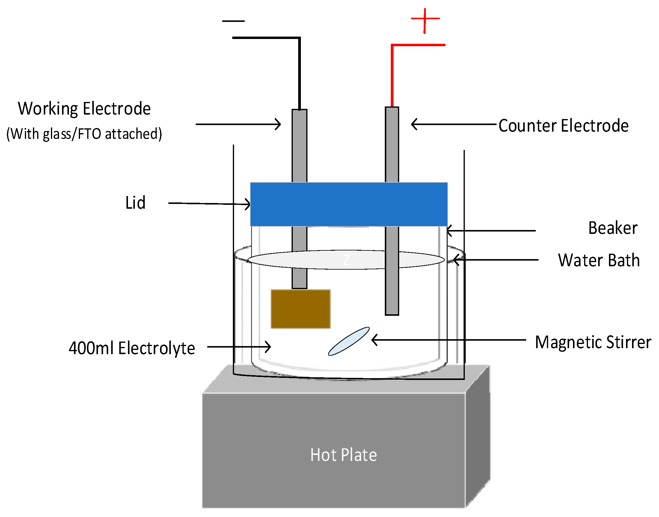
23] on glass/(FTO) substrates with 7 Ω/□ sheet resistance. The electrochemical setup used is shown in
Figure 1.
An electrolytic solution was prepared by dissolving 0.5 mM Sb2O3 (99.999%) and 0.1 mM SeO2 (99.999%) in 20 mL of sulfuric acid. The solution was stirred for three hours to enable the solution to mix completely and for the solute’s dissolution. The acid precursor solution was then heated at 160 °C for 2 h and allowed to cool to room temperature. The cold solution was then diluted with 400 mL deionized water (>15 Mohms.cm Pure Lab Chorus, ELGA) in a polytetrafluoroethylene (PTFE) beaker placed in a water bath, and the whole setup was placed on top of a magnetic hot plate with a magnetic stirrer, stirring continuously at a 120 rpm stirring rate, and maintained throughout the experiment. The process involved heating the solution to 200 °C and maintaining it at this temperature until it became transparent, which took approximately 4 h. Subsequently, the solution was subjected to a lower temperature heating (120 °C) for the next 48 h before initiating the electrodeposition process. Throughout the heating and setting of the electrolyte solution, deionized water was periodically added to both the electrolyte and the bath to maintain a constant solution homogeneity and volume (400 mL). This addition of water served to compensate for the portion of the electrolyte loss via evaporation since the bath is covered with a lid having three holes, where two served for the electrodes, while the third for de-pressuring the bath, thereby preventing too much evaporation during the extended heating period. Pure carbon rods were used as electrodes. The growth temperature was maintained at 85.0 ± 0.2 °C. Even though the higher growth temperature is desired for semiconductors, this growth temperature is limited by the boiling point of water.
Before the electrodeposition, the substrate was cut into 1 × 2 cm
2 sizes, cleaned using cotton buds and detergents, ultrasonically cleaned using deionized water (or ELGA deionized water of 15 MΩ.cm resistivity), acetone/alcohol was used to degrease the surface, and then rinsed again with deionized water. Then, the substrates were allowed to dry under nitrogen gas (N
2) flow. The glass/FTO slide was then attached to the cathode electrode using a PTFE tape before connecting to a computer-controlled potentiostat (Gill AC, ACM instruments, Cumbria, UK). All chemicals used were of high purity grade and purchased from Sigma Aldrich (MERCK, Gillingham, UK). H
2SO
4 and NH
4OH were used to maintain the pH at 2.0 ± 0.2. Cyclic voltammetry was carried out to determine the growth voltages required for the electrodeposition. This is a first-step approach for the growth of any quality thin-film semiconductor material via the electrodeposition route. Cyclic voltammetry enables the identification of the range of growth potentials required for the electrodeposition and the potential at which hydrogen gas starts evolving. This is because too much hydrogen evolvement could hinder or mar uniform layer growths and cause serious thin-film surface non-adhesion and de-lamination. However, some generation of hydrogen during the growth of the material could be beneficial in the reduction of defects through passivation. Using the potentiometer, different voltages were applied to the electrodes, and the current density through the electrolyte was monitored in both forward and reversed directions while a constant medium stirring rate was maintained. The current versus voltage graphs (voltammogram) were plotted, which enabled the determination of the range of growth voltages required for the electrodeposition process. The voltage range was subdivided as per the number of different semiconductor layers to be grown, as shown in
Figure 2.
Electrodeposition was carried out at constant cathodic potential for an average time of 20 min. The electrodeposition growth’s duration depends on the electrolyte’s concentration, the growth’s voltage, the heat applied, the electrolyte’s stirring rate, and the resistivity of the substrate layer. The images of Sb
2Se
3 samples deposited at different fixed voltages per growth are shown in
Figure 2.
The electrodeposition method provides a good platform for controlling material properties (optical, structural, morphological, and electrical), which could be achieved by adjusting the preparative parameters such as growth voltage, temperature of the electrolyte, pH, precursor concentrations, stirring rate, deposition time and the ability to master the post-deposition annealing temperature. While bearing in mind that the key requirement is that the substrate must be conductive, e.g., conductive glass/FTO.
Electrodeposited layers at ~85 °C are not suitable for fabrication of electronic devices. These must undergo post-deposition heat treatments to improve their structural, morphological, electrical, and optical properties. However, considering the effect of heat treatment temperature employed during annealing, an addition of heat above a minimum threshold could lead to a total disintegration of the sample material. This is because annealing temperature has a direct bearing on the re-crystallization or disintegration of the sample material. Hence, the minimum temperature required for annealing may vary from material to material, the kind of material growth used, precursors making up the electrolyte, and its concentration, electrolyte’s stirring rate, precursor solutes, manner of electrolyte formation or formulation, and duration of the sample growth. In this research, after numerous experimentations, layers of Sb2Se3 materials were heat treated at 150 °C for 2.25 h to complete reactions between the unreacted Sb and Se. Then, a second stage of heat treatment at 350 °C for 15 min was carried out to improve the crystallinity of the material layers.
Different analytical methods, such as photoelectrochemical cell (PEC) measurements, Optical absorption spectroscopy, X-ray diffraction (XRD), Scanning Electron Microscopy (SEM- Quanta 650), and Raman microscopy (DXR2), were used to characterize the samples produced.
PEC is a technique used for the measurement of the electrical conductivity type of the grown Sb
2Se
3 semiconductor material and can be performed for any other thin-film samples grown on conductive substrates. To make this measurement, a 0.1 M aqueous solution of sodium thiosulfate (Na
2S
2O
3) was made into a 20 mL beaker of deionized water, as shown in
Figure 3.
The sample was attached to a pure carbon electrode, and another carbon rod was used as the counter electrode. The two electrodes were completed by connecting with an external digital voltameter. A solid/liquid interface was created between the semiconductor thin film and the Na2S2O3 electrolyte solution by immersing the layer in the liquid solution. This acts as a simple Schottky contact, and the corresponding voltages were recorded under illumination (VL (mV)) and under darkness (VD (mV)) conditions. Differences between the two individual voltages give the photoelectrochemical cell (PEC) measurement in millivolt. This is, in fact, the Voc of the solid/liquid junction. The sign of the PEC signal represents the conductivity type, while its magnitude indicates the doping concentration of the semiconductor material.
UV-Vis optical spectrophotometry is a technique used to carry out measurements of the optical absorption of semiconductor materials. In this work, the ultraviolet-visible spectrophotometer (Cary 50 Scan UV-Vis Spectrophotometer) was used, and the absorption spectra wavelengths used ranged between 190 and 2500 nm. The results obtained were later analyzed using Tauc plots.
Considering the expression in Equation (2), the Tauc plot was obtained by plotting (ahʋ)
2 against the light energy hʋ (eV). Where A-is the absorbance,
h is Planck’s constant, m = 1/2 is for the direct bandgap semiconductor materials, and T is the percentage (%) transmittance [
9].
Tauc equation expresses a relationship between the incident photon frequency (ʋ), Planck’s constant (h), and the optical energy bandgap (Eg). Extension of the straight-line portion of the Tauc plot provides a possible energy bandgap of the material.
X-ray diffraction (XRD) was utilized to characterize the crystal structure and phase composition of the synthesized Sb2Se3 thin film materials. The XRD measurements were performed at room temperature using PANalytical X’Pert diffractometer (Worcestershire, UK) with Cu Kα radiation (λ = 1.54 Å) as the X-ray source, shape factor (K = 0.9) assuming spherical crystallites. The X-ray diffractometer was set at 2 θ = 41.131°, Omega offset = 15.563°, Goniometer = PW3050, resolution = normal 0.001°, sample stage = spinner pw3064. Voltage and current generator were set at 40 kV and 40 mA, respectively, while the instrument broadening was described by the full width at half maximum (FWHM). The thin film samples were mounted on a low background silicon sample holder and scanned over a 2 θ range of 0–90° with a step size of 0.02°. The resulting diffraction patterns were analyzed to identify the crystalline phases present based on the peak positions and intensities. Structural parameters such as lattice constants, grain sizes, dislocation density, and preferred orientations could be extracted from the XRD data by profile fitting and application of the Scherrer equation.
The XRD characterization provides insights into the crystallographic structure of the Sb2Se3 thin film materials. Bragg’s law is used in the field of X-ray diffraction to describe the relationship between the wavelength (λ) of incident radiation, the spacing between atomic planes (d) in a crystal lattice, and the angle (θ) at which the radiation is scattered or diffracted by the crystal lattice.
Bragg’s law is fundamental in determining the angles at which diffraction peaks occur within the crystalline lattice.
The Debye–Scherrer equation plays a fundamental role in the precise determination of material crystallite sizes.
In tandem with the Debye–Scherrer equation, the Scanning Electron Microscopy (SEM) technique stands out as a valuable tool for the assessment of crystal grain sizes. This technique is further enhanced through Energy-Dispersive X-ray Analysis (EDX), which not only confirms the presence of constituent elements within the Sb2Se3 material but also validates their authenticity.
In addition to SEM and EDX, Raman Spectroscopy measurements were conducted on the Sb
2Se
3 material. This non-destructive analytical method is pivotal for investigating vibrational modes within materials. It relies on the phenomenon of inelastic scattering of monochromatic light, typically emitted from a laser source [
24].
3. Results and Discussion
3.1. Cyclic Voltametric Study
Figure 4 displays a representative voltammogram of the electrolyte employed in this study. Notably, when considering the electrode potentials, antimony (Sb) registers a potential of +0.21 V, whereas selenium (Se) exhibits a higher potential at +0.74 V. Interestingly, the voltammogram reveals that Se commences its deposition on the glass/FTO substrate prior to Sb, despite Sb having a lower electrode potential.
Specifically, in the cyclic voltammetry plot, Se’s deposition initiates at a relatively low voltage of approximately 348 mV, whereas Sb’s deposition commences at a higher voltage, around 700 mV. It is important to highlight that the onset of hydrogen gas evolution falls within the voltage range of 1230 mV to 1500 mV [
1]. This early hydrogen evolution at lower voltages plays a crucial role in semiconductor layer growth by passivating material defects and contributing to the formation of a uniform thin-film layer.
However, it is worth noting that at higher voltages, around 2250 mV, the electrochemical bath experiences thin-film surface layer de-lamination, attributed to an intensified hydrogen gas evolution process. Consequently, the voltage range of 1600 mV to 1950 mV has been identified as the suitable range for achieving Sb
2Se
3 thin-film semiconductor layers, as exemplified in
Figure 2. Layers of the Sb
2Se
3 semiconductor materials grown consist of mixtures of Sb
2Se
3 and unreacted Sb and Se elements due to low-temperature growth. Profilometry shows that layers grown for ~20 min at ~1740 mV have an average thickness of ~1.68 µm. Therefore, annealing was carried out to improve the material crystallinity.
3.2. Photoelectrochemical Cell Measurement (PEC)
Since the material was grown on top of conductive substrates (FTO), other conductivity-type measurement techniques are not feasible here. Thus, the photoelectrochemical cell measurement (PEC) technique was used to determine the electrical conduction type of the Sb2Se3 semiconductor material.
The PEC system utilized in this study (as depicted in
Figure 4) was meticulously calibrated using standard materials of known electrical conduction Types, such as n-Type cadmium sulfide (CdS) [
17,
25]. This calibration served as a critical baseline reference for subsequent measurements.
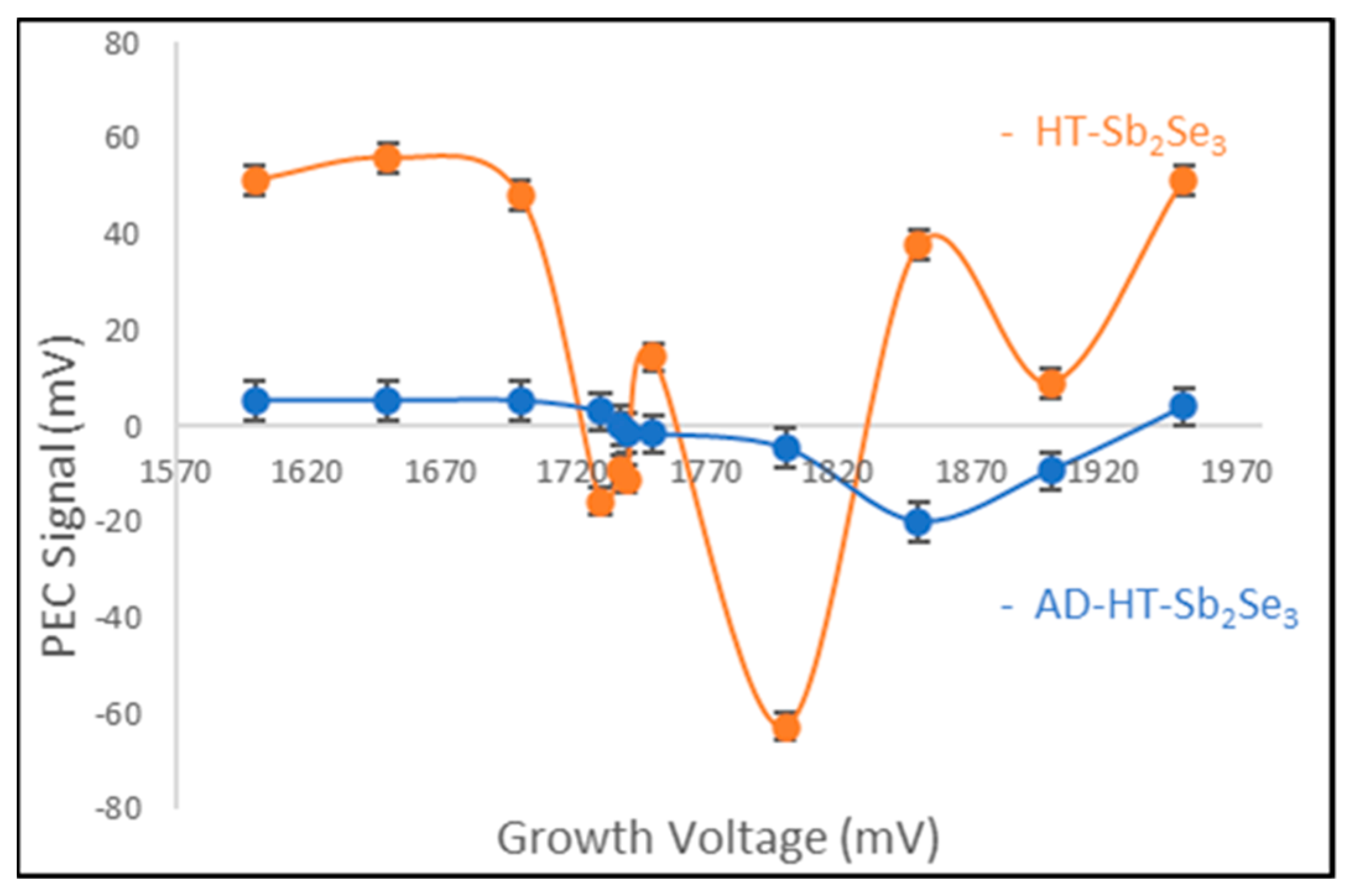
Figure 5 presents PEC results for AD-deposited (AD) and post-deposition heat-treated (HT) Sb
2Se
3 thin film samples grown by electrodeposition at ~85 ± 0.2 °C. The HT-Sb
2Se
3 curve corresponds to Sb
2Se
3 films after annealing, while the AD-Sb
2Se
3 curve is for the AD-deposited films prior to heat treatment. At the low 85 °C growth temperature, the AD-Sb
2Se
3 films are expected to contain unreacted Sb and Se elements rather than the fully formed Sb
2Se
3 semiconductor material [
10]. Thus, the AD-Sb
2Se
3 films do not provide reliable electrical characterization. However, after 150 °C heat treatment for 2.25 h and 350 °C re-heat treatment for 15 min, respectively, the Sb and Se unreacted elements are expected to fully react to form Sb
2Se
3 [
26,
27], as shown in
Figure 5.
Thus, it becomes evident that by varying the growth potentials of the material, both the conductivity types can be measured directly from the same electrochemical bath without the need for any external dopants. These distinct conductivity types are a reflection of the stoichiometry of the thin film layers. For instance, as seen in
Figure 5, when we examine the AD-Sb
2Se
3 curve, it is apparent that p-Type Sb
2Se
3 semiconductor materials were produced at lower growth potentials. This occurrence can be attributed to a positive PEC signal obtained from the potential difference between the voltage measurements under the dark (V
D) and under illumination (V
L). This may happen due to the presence of more selenium in the material. Conversely, at higher growth potentials, the materials exhibit n-Type conductivities due to the presence of more antimony in the layers. The critical insight here lies in the intrinsic point, which occurs around a growth potential of ~1740 mV for this electrodeposition bath. This intrinsic point signifies the deposition of stoichiometric material at this growth voltage (equal deposition of both Sb and Se on the glass substrate) [
28]. Generally, the materials grown within this voltage are characterized by high crystalline grains, slower growth rate, and good material quality. The more crystalline a semiconductor material is, the better it can be considered for use in making high-quality photovoltaic solar cell devices.
The HT-Sb2Se3 layers also exhibit the same trend of electrical conductivity types up to ~1800 mV. However, the layers grown above this voltage show an unexpected behavior, most probably due to the introduction of unwanted chemical reactions taking place at higher voltages during electrodeposition. The exact reason for this return to p-Type electrical conductivity is not known at present. In the case of electronic device fabrication, both p-Type and n-Type materials can be grown from the same electrolyte between the 1600 mV and 1800 mV voltages.
3.3. Optical Absorption
The energy bandgap is a key optical property of semiconductor materials that determines their electrical and optical behavior. In this work, the bandgap of antimony selenide (Sb
2Se
3) thin films fabricated via electrodeposition was investigated in the AD-deposited and annealed states using UV-Vis spectrophotometer (UV-3600 plus, 00687 SHIMADZU, Kyoto, Japan). AD-deposited Sb
2Se
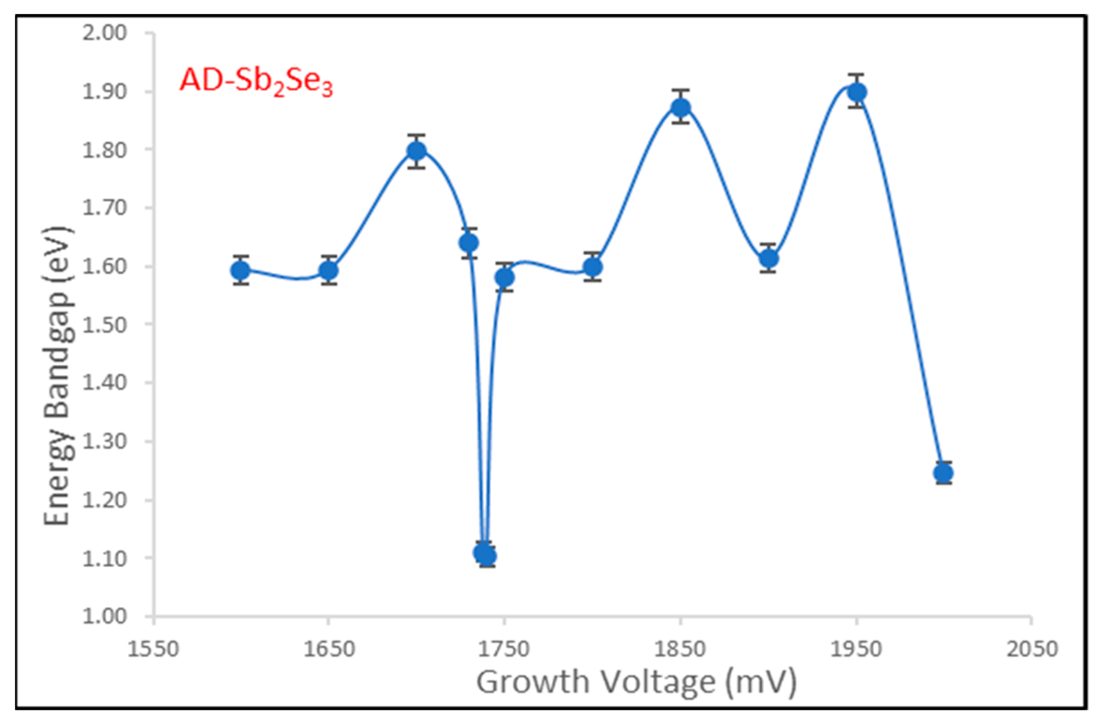
3 films are expected to contain unreacted, nanostructured Sb and Se phases, as shown in
Figure 6 and
Figure 7 where the dotted lines intercepting with the horizontal axis of the two figures give the respective optical energy bandgap reading for each material curve.
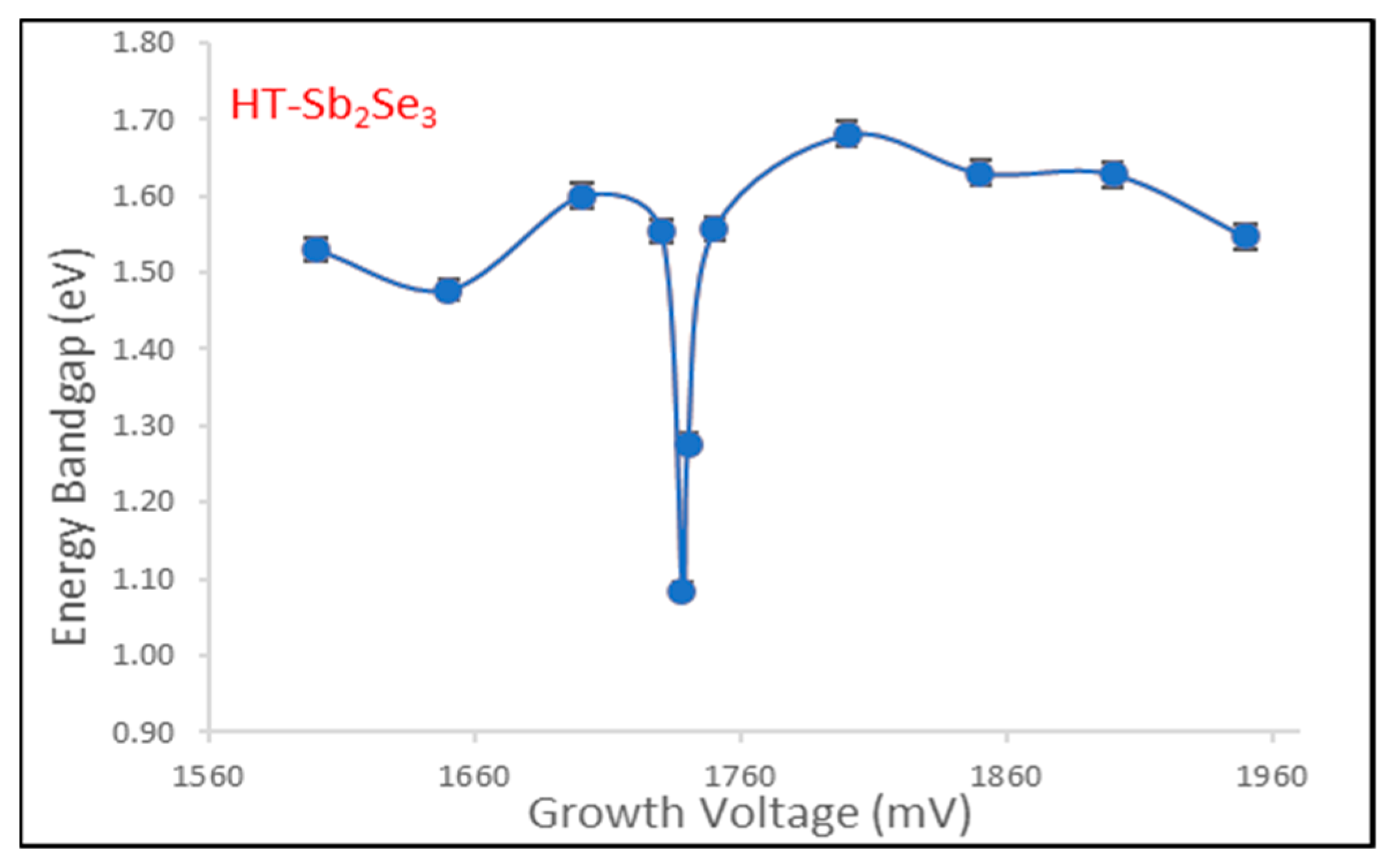
Annealing enables full reaction to form Sb
2Se
3 crystalline phase in
Figure 8 and
Figure 9.
Optical absorption measurements were performed at room temperature over a spectral range of 190–2500 nm. Tauc plots of (αhν)
2 versus photon energy (hν) were plotted to estimate the optical energy bandgap, e.g., by extrapolating the linear region to the x-axis intercept [
4,
19]. The Tauc plot analysis (
Figure 6,
Figure 7,
Figure 8 and
Figure 9) revealed a wide energy bandgap range of 1.10–1.90 eV for AD-Sb
2Se
3 and a narrow bandgap range of 1.08–1.68 eV for the annealed Sb
2Se
3 thin films. The convergence in bandgap values following heat treatment suggests improved crystallinity and Sb
2Se
3 phase formation, which is consistent with XRD analysis. The wider energy bandgap distribution in the AD-deposited state may be attributed to quantum confinement effects arising from the unreacted, nanoscale Sb and Se particles. Overall, the results demonstrate that the bandgap can be tuned by controlling the deposition and annealing parameters during Sb
2Se
3 thin film fabrication.
Figure 7 and
Figure 9 show the dependence of optical bandgap energy (Eg) on the deposition voltage for both AD-deposited and heat-treated Sb
2Se
3 thin films fabricated via electrochemical deposition. The bandgap values were the average values obtained from Tauc plots based on optical absorption measurements, as described previously. As the applied voltage during electrodeposition growth increases from 1600 mV to 2000 mV, the resulting bandgap of the annealed Sb
2Se
3 films remains relatively constant in the narrow range of 1.08–1.68 eV. The constant ~1.28 eV Sb
2Se
3 bandgap aligns well with reported values for bulk crystalline Sb
2Se
3 semiconductor materials [
4,
20].
3.4. X-ray Diffraction (XRD) Spectroscopic Analysis
XRD measurement allows the determination of the level of crystallinity of Sb
2Se
3 semiconductor materials produced by electrodeposition.
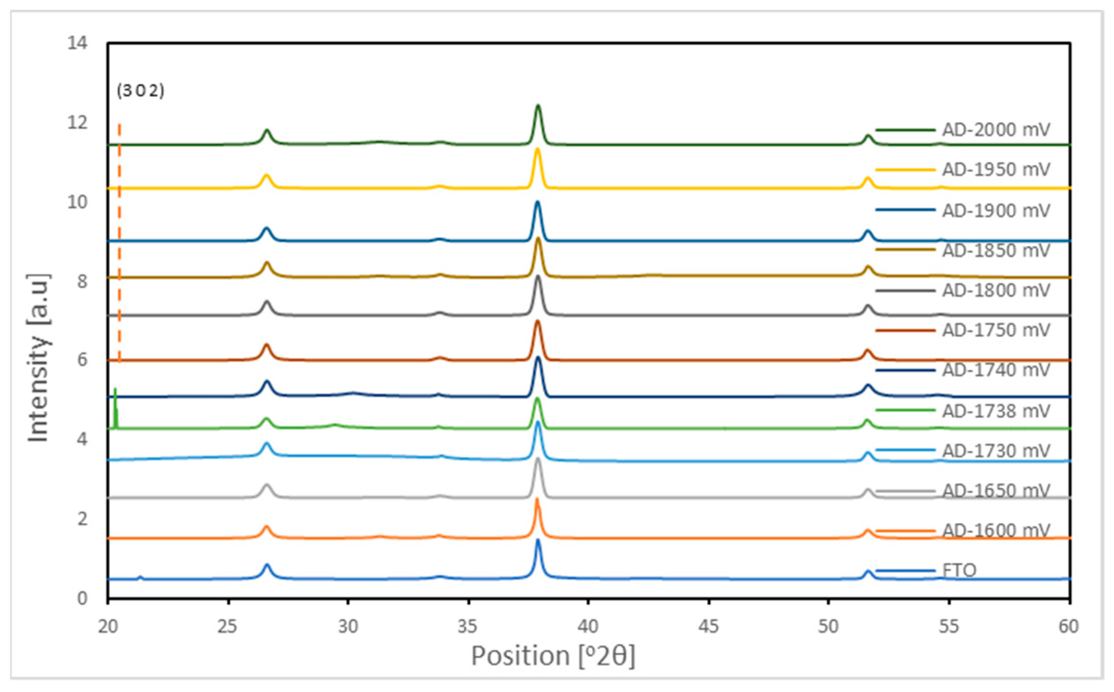
Figure 10 shows the X-ray diffraction patterns for AD-deposited Sb
2Se
3 thin films grown by electrochemical deposition at various voltages. This material appeared to be characterized by amorphous nature as there seemed to be no observable peaks before annealing. Annealing can undoubtedly reduce the number of bulk defects and grain boundaries that can catalyze recombination [
4,
21].
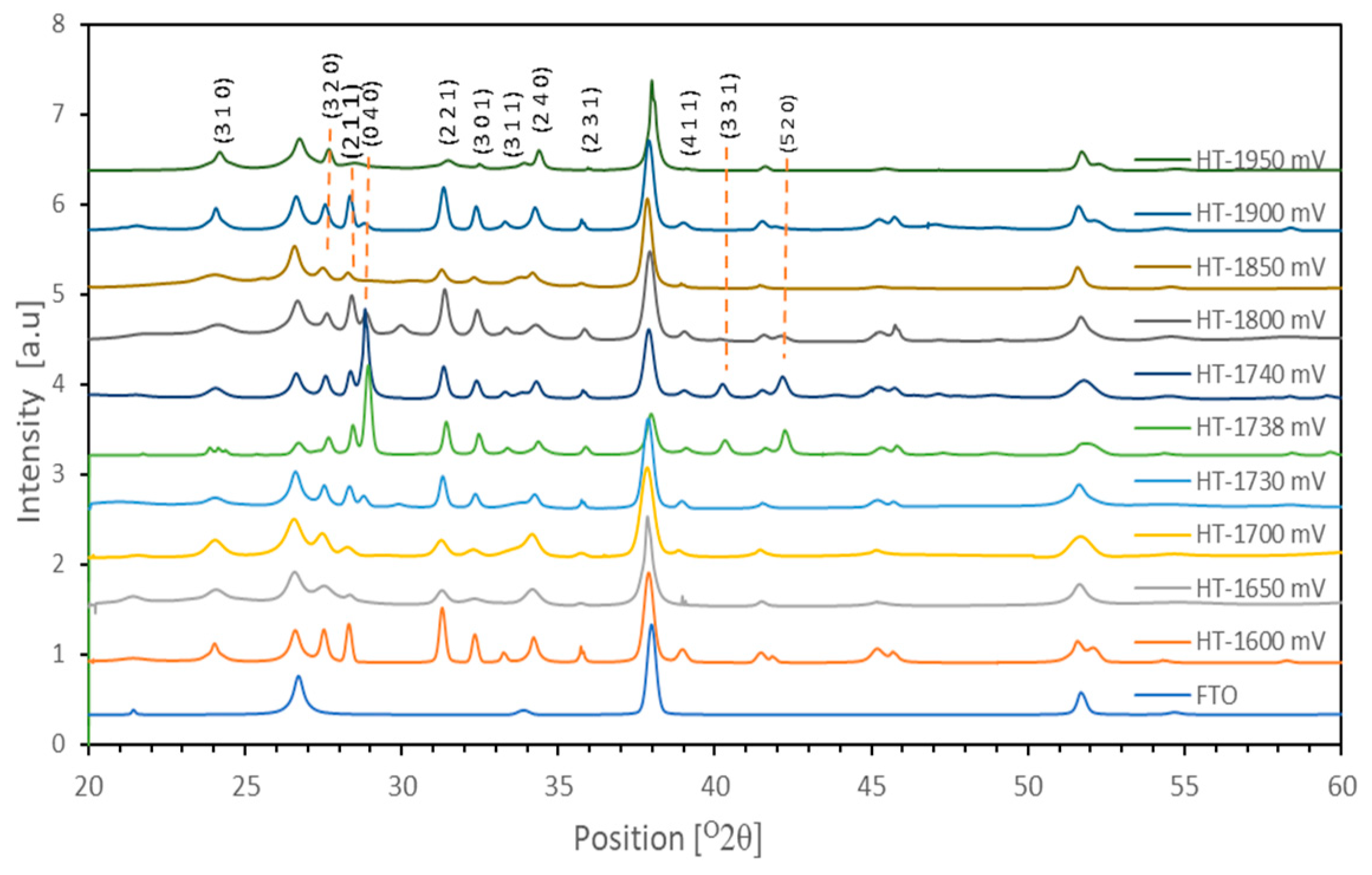
At the defined deposition voltages of 1740 mV, 1738 mV, and 1600 mV, the Sb
2Se
3 phase formation appears more defined and crystalline based on the sharper (211) peaks (
Figure 11). The broader peaks around 24°, 36°, and 45° indicate lower intensities around those voltages, implying reduced crystalline quality, which may be attributed to kinetic effects favoring amorphous film growth.
Additionally, the presence of unreacted Sb and Se is evident from the amorphous AD-Sbe
2Se
3 XRD patterns and supported by EDX analysis [
29]. This incomplete reaction is expected for films deposited at the low temperature of ~85 °C. Estimated grain sizes from Scherrer analysis range from 106 to 365 nm across the various voltages (
Table 1). Overall, the XRD/EDX results confirm the successful formation of nanostructured crystalline Sb
2Se
3 thin films with preferential (2 2 1) and (0 4 0) orientation in the heat-treated state.
Apart from the (310), (320), (211), (301), (311), (221), (040), (240), (231), (411), (331), and (520) peaks, other peaks correspond to the FTO substrate. To increase the material crystallinity, two-stage heat treatment conditions were utilized where the samples were first heat treated at 150 °C for 2.25 h to react with the unreacted elements (Se and Sb). The material was allowed to cool down to room temperature, and layers were re-heated at 350 °C for another 15 min to increase the semiconductor material’s crystallinity.
After the heat treatments in air, the XRD measurements were repeated for these materials.
Figure 11 shows how the micrographs have greatly improved, with better peaks portraying improved crystalline quality for these samples. This is possible because the remaining unreacted elements seemed to have now completely reacted as depicted in the crystalline XRD peaks, and the amorphous nature of these elements has completely disappeared with now intense peaks (
Figure 11) arising especially for the growth samples 1600 mV, 1738 mV, and 1740 mV, which had diminished peaks of zero intensity before annealing, but now developed into stronger intensity peaks after annealing. The films exhibit diffraction patterns that can be indexed to the crystalline Sb
2Se
3 phase (JCPDS 01-089-0821), which is orthorhombic.
The prominent peaks (211) reflections around 2 θ = 28°, 31° and (0 4 0) 2 θ = 28.9° indicate preferred orientations along this plane. The weak peaks such as the (3 1 0), (3 1 1), (2 3 1), and (4 1 1) around 2 θ = 24.3°, 33.3°, 35.98°, and 39.18° suggest random crystallite orientations perpendicular to the substrate.
Grain sizes were estimated using Debye–Scherrer’s equation, and the results for all layers were tabulated. Scherrer’s equation used in this analysis is
where D is the crystallite size,
is the full width at half maximum in radians, θ is the Bragg angle in degrees, and λ = 1.54 Å is the wavelength of X-rays used [
30].
Details of the XRD results for HT-Sb
2Se
3 layers are recorded in
Table 1. Since AD-Sb
2Se
3 layers do not exhibit any well-developed XRD peaks, only the heat-treated samples are reported here.
Even the 1730 mV sample, which had no visible material peak before annealing, now developed some peaks, though with a crystallite size of 106 nm, smaller than the other material peaks. This shows how significant it is for a scientist to ensure an optimum annealing condition is established before selecting the final material that can be used in the making of PV devices. From
Table 1, 1600 mV, 1738 mV, and 1740 mV sample growths have shown good promise for use in the making of high-efficiency solar cell devices. This is because they have better crystalline grain quality, as evidenced by the calculated crystallite sizes. The more crystalline a material is, the better it can be used in the making of high-efficiency photovoltaic solar cell devices [
5,
31].
where δ is the dislocation density in nm
−2 and ϵ is the microstrain, which is dimensionless.
Dislocation density (δ) refers to the imperfection in the crystal lattice due to the misalignment of the lattice points from their reference positions, which can occur randomly [
32,
33].
Systematic heat treatments performed on the Sb2Se3 material clearly improve the material quality. Results indicate a significant reduction in lattice imperfections in the material, as evidenced in the reduction in dislocation density due to material quality improvements, thanks to the systematic approaches followed during annealing. Quantitative XRD analysis revealed that heat treatments result in a notable decrease in defects and dislocations, leading to enhanced crystallinity and improved perfection of the lattice structure. The data provide comprehensive evidence on the enhancement of the structural order and quality of the Sb2Se3 material.
3.5. Scanning Electron Microscopy (SEM) Analysis
A scanning electron microscope (FEI Quanta 650, Oregon, OR, USA) was used to study the surface morphology, range of grain sizes, and microstructure of the thin-film Sb
2Se
3 semiconductor material.
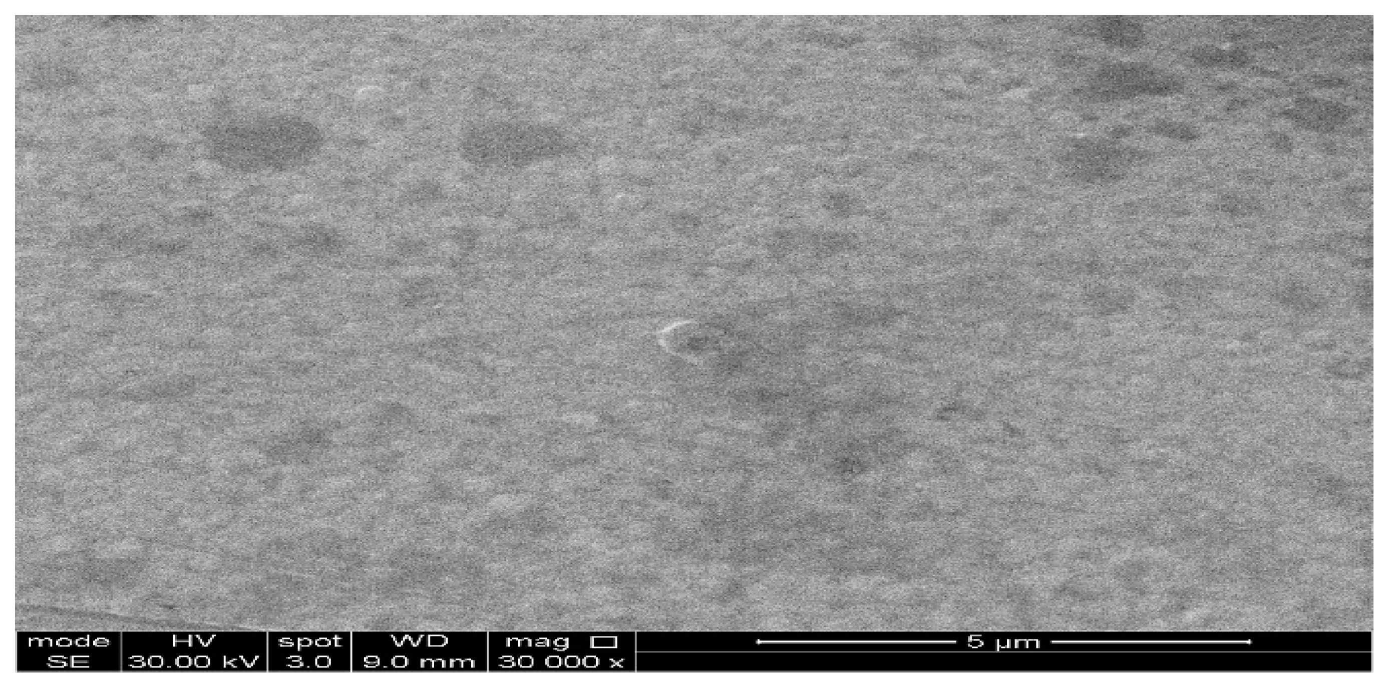
Figure 12,
Figure 13,
Figure 14 and
Figure 15 showed different images captured for both AD-deposited and heat-treated Sb
2Se
3 semiconductor materials. The Sb
2Se
3 thin-film grains appeared as small discrete nanoparticles with uniform irregular shapes and fewer grain boundaries but well-defined facets. This clearly agglomerates to forming large grain structures, as clearly seen in the grain clusters in
Figure 12. This material appeared to have very little grain porosity or voids, as the grain cluster intercalation appeared rigid and uniform. The morphology appeared uniform, with an average grain size of 3.26 µm.
The Sb2Se3 thin film appeared to be made up of larger grains, which occurred because of the agglomeration of smaller crystallite grains.
In
Figure 14, the average grain sizes are presented for the annealed Sb
2Se
3 material that was grown at 1738 mV. Additionally, an Energy Dispersive X-ray (EDX) analysis of the Sb
2Se
3 thin-film layer at 1738 mV reveals the presence of individual constituent elements atop the glass/fluorine-doped tin oxide substrate.
Within this analysis, it is evident that calcium (Ca) and silicon (Si) constituents are derived from the glass substrate, whereas the presence of carbon (C) can be attributed to the carbon electrodes employed during the electrodeposition process. This layer, as depicted, provides a comprehensive representation of the compositional distribution of these constituent elements within the sample’s cross-section.
3.6. Energy Dispersive X-ray (EDX) Spectroscopy
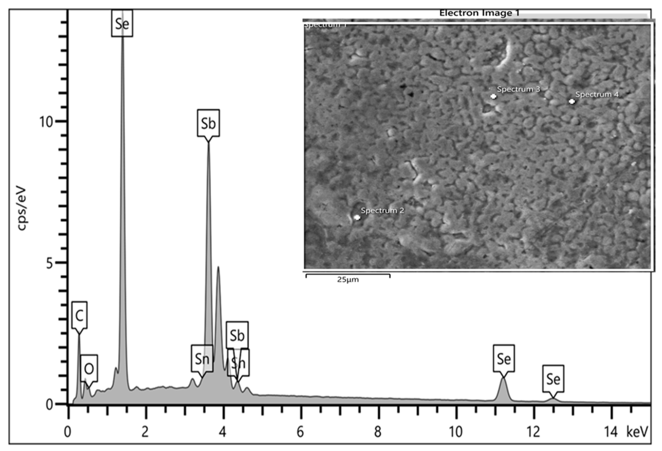
Energy Dispersive X-ray spectroscopy (EDX) attached to Quant 650 was used for the compositional analysis of the atomic elements present in the sample material via the use of Aztec software (version 6.0). The below spectra captured at the different parts of the 1738 mV Sb2Se3 growth show the presence of both constituent elements, Sb and Se, at reasonable proportions.
Thus, it was confirmed that the material grown is basically Sb
2Se
3 as confirmed by the spectra in
Figure 16. The insert showed some of the spectra captured during meticulous measurements.
The compositional weight percent (wt%) ratio between Sb and Se computed is approximately 1. This indicates the stoichiometric uniformity of the individual elemental formation of the Sb
2Se
3 semiconductor material on the thin-film layer,
Table 2.
3.7. Raman Spectroscopy
Raman spectroscopy is an efficient and non-destructive characterization technique utilized for the identification and investigation of molecular fingerprints, crystallinity, strain, and stress of semiconductors or solid-state materials. This technique relies on the inelastic scattering of monochromatic light, mainly laser sources ranging from ultraviolet (244–380) nm through visible (380–750) nm to near-infrared (750–900) nm.
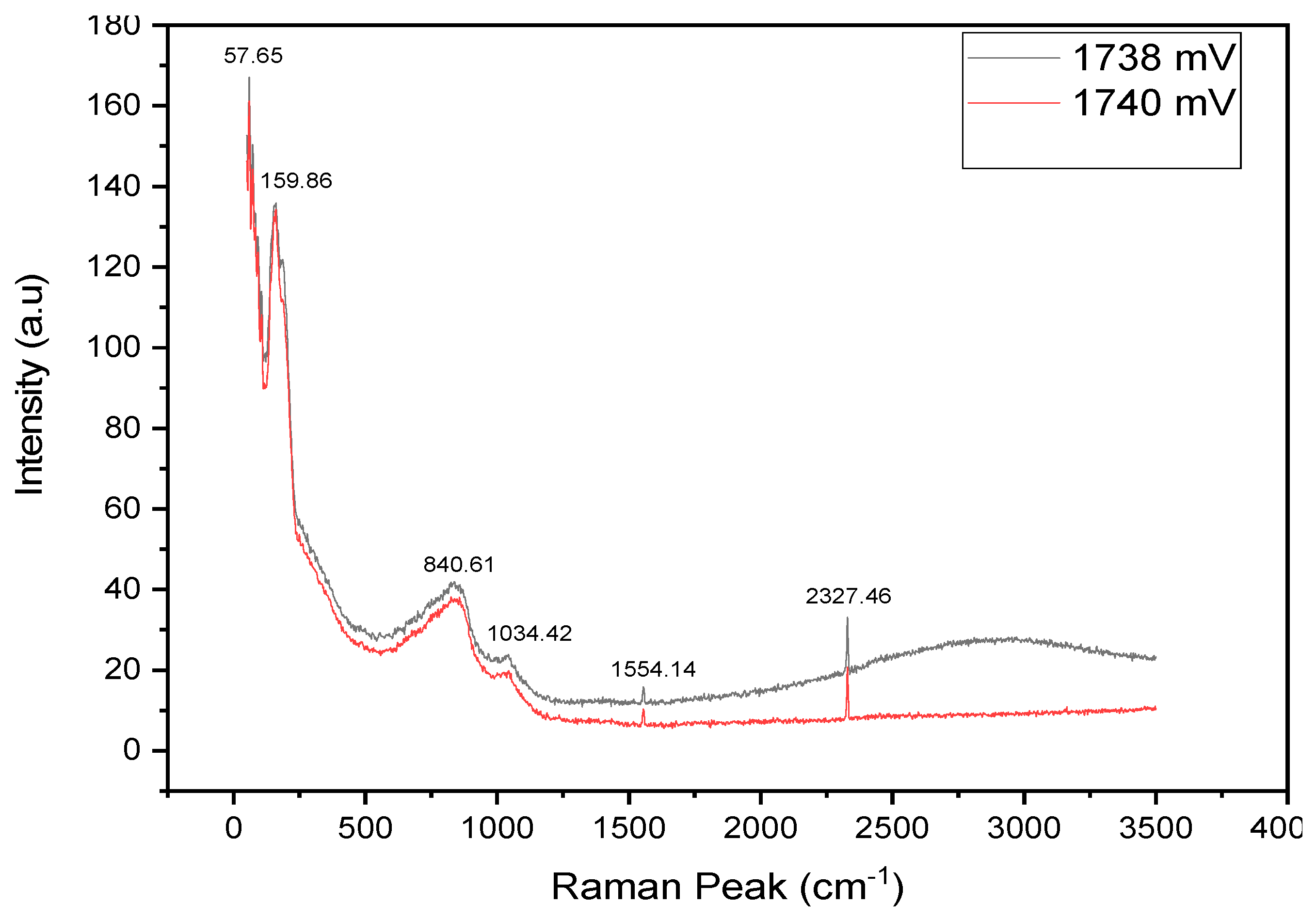
In this research study, DXR-2 Raman Microscope equipped with a 10× objective and a 50-micron slit size was employed. The choice of excitation source was a HeNe laser line with a wavelength of 633 nm. This setup was used to perform scans on the two best material layers of HT-Sb
2Se
3 samples grown at voltage potentials of 1738 mV and 1740 mV.
Figure 17 shows that the Raman modes for the 1738 mV and 1740 mV are very similar, except for the hump observed for the 1738 mV sample between the Raman peaks 2500 cm
−1 and 3500 cm
−1. This highlights that the optimum growth voltage is at 1740 mV.
During these scans, 8 mW laser power was applied and carefully controlled to avoid any damage to the sample material. Results analysis revealed the presence of distinct longitudinal optical vibration peaks (LO) at 57.65 cm−1, 159.86 cm⁻1, 840.61 cm−1, 1034.42 cm−1, 1554.14 cm−1, and 2327.46 cm−1.
This experimental setup and observation provide valuable insights into the vibrational properties of the Sb2Se3 semiconductor material and contribute immensely to the understanding of its unique characteristics. Longitudinal optical (LO) phonons are vibrations in a solid in which atoms oscillate back and forth along the direction of propagation of the wave. LO phonons interact strongly with light, leading to a coupling between LO phonons and electromagnetic waves in polar crystals.
The crystalline phase identification was complemented with the XRD measurements (
Figure 10 and
Figure 11), and the results indicate that it belongs to the pbnm (62) space group with an orthorhombic crystalline phase. In this research, the 57.65 cm
−1 and 150.86 cm
−1 Raman spectra displayed peaks have been confirmed to be among the dominant peaks commonly assigned to the Sb
2Se
3 phase [
29,
34].
