Article

Efficiency and PF Improving Techniques with a Digital Control for Totem-Pole Bridgeless CRM Boost PFC Converters

Department of Electronic Engineering, Hanbat National University, Daejeon 34158, Republic of Korea
Energies 2024, 17(2), 369; https://doi.org/10.3390/en17020369
Submission received: 10 December 2023 / Revised: 5 January 2024 / Accepted: 9 January 2024 / Published: 11 January 2024
(This article belongs to the Section F3: Power Electronics)

Abstract

:
A totem-pole bridgeless boost converter is one of the most promising topologies for the power factor correction (PFC) stage in high-power applications due to its high efficiency and small number of components. However, due to the totem-pole structure of the field-effect transistor (FET), very high switching loss occurs via the reverse recovery current of the body diode. To solve these problems, critical mode (CRM) control is a good solution to achieve the valley switching technique. With valley switching of CRM control, the switching loss decreases drastically with decreasing turn-on voltage. But, although the CRM control enables valley switching, it is hard to make an exact valley switching control with general zero-voltage detection circuits. In addition, when a frequency limitation scheme is applied to prevent a very high frequency, the switch can operate with hard switching at the boundary of the frequency limitation. Furthermore, the CRM boost PFC has a low PF and high total harmonic distortion (THD) under light-load conditions due to the large negative current resulting from resonance between the inductor and parasitic capacitance. It becomes worse at near-zero input voltage since the resonance current becomes larger near zero-input voltage. Therefore, in this paper, a totem-pole bridgeless boost PFC converter with high efficiency, high PF, and low THD is developed using TMS320F28377 by Texas Instruments. Based on the basic digital structure of the totem-pole bridgeless converter, the proposed controls help with exact valley switching, PF and THD improvement, and frequency limitation. The prototype converter is verified using 90–264 VAC input voltages and 450 V/3.3 kW output specifications.

1. Introduction

The era of global warming has ended and “the era of global boiling has arrived”, the United Nations (UN) Secretary-General said at the UN headquarters in New York City. Although humanity has experienced significant growth and progress through technological advancement, as society continues to evolve, there is a growing concerning about increasing environmental pollution. Naturally, there has been a growing demand for eco-friendly electric vehicles (EVs), and it stimulated the development of various EV components [1,2,3].
Among the various EV components, an on-board charger (OBC) performs an important role since it charges the battery of an EV. In general, the OBC is composed of a two-stage structure, consisting of power factor correction (PFC) and DC/DC converter [4,5,6,7]. For the PFC stage, the boost converter shown in Figure 1 is usually used since it has a simple structure, and, for the DC/DC stage, a phase-shifted full-bridge converter and an LLC resonant converter are used because they have high efficiency for high-power applications, such as with an OBC [8,9,10,11].
However, as the output power increases due to an increase in battery capacity, high efficiency becomes more important to reduce thermal problems. Therefore, to improve the efficiency of the PFC stage, the conventional boost PFC stage was changed to have high efficiency in the high-power stage. As a result, totem-pole bridgeless boost converters (shown in Figure 2) are increasingly being used in high-power applications, such as in OBCs, to have a high efficiency. The totem-pole bridgeless boost converter is a type of bridgeless boost converter. Among the various bridgeless boost converters, it has high efficiency and low common-mode (CM) noise compared [12,13,14,15,16,17]. But, due to the totem-pole structure of QB1 and QB2, a reverse recovery current of QB1 flows to QB2 when QB1 is turned on in the positive cycle, which causes large switching loss at QB2 [18,19,20]. The reverse recovery current of QB2 also flows to QB1 when QB2 is turned on in the negative cycle of the input voltage.
To solve this problem, the CRM control of the totem-pole bridgeless boost converter is a good candidate. With CRM control, QB1 and QB2 are turned off at zero current, and it does not cause reverse recovery current. In addition, since CRM control enables zero-voltage switching or valley switching, it has low switching-loss compared to continuous conduction mode (CCM) control. However, CRM control has some limitations: Firstly, although CRM control can achieve valley switching, it is hard to achieve an exact valley switching operation with basic zero current detection (ZCD) circuits. In addition, CRM control has a large current distortion under light-load conditions due to resonance between the inductor and parasitic capacitance, resulting in a low power factor (PF) and high total harmonic distortion (THD). Furthermore, since CRM control causes very high switching frequency near zero voltage, it is general to limit the maximum switching frequency. But, when the converter operates near maximum frequency, the hard switching can be occurred resulting in high switching loss.
Various studies have aimed to solve the aforementioned problems of CRM operation. In [21,22,23], research was conducted to achieve exact valley switching with a basic ZCD circuit. In [21], new timer circuits were proposed to achieve the optimal valley switching point inCRM operation. As shown in Figure 3, a ZCD circuit uses auxiliary winding to sense the inductor voltage VLB1. It is transferred to the ZCD circuit as VLB2, which is scaled down and has reverse polarity. Finally, VZCD voltage is made by eliminating the negative voltage of VLB2. And, voltage dividing resistors and clamp diodes are required to limit the voltage for digital IC. As a result, when VZCD becomes zero, in which the inductor current also becomes zero, the gate signal of QB2 is turned on. However, the exact point where VZCD becomes zero occurs when the resonant current between inductor and output capacitance of MOSFET is at its peak value. Since the resonant current helps the valley switching of the MOSFET, gate signal QB2 should be turned on when resonant current becomes zero at t4, which is the optimal point. Therefore, in that paper, the author used timer circuits to cause a time-delay until that optimal point. In [22], the study also used a basic ZCD circuit, which senses an inductor current with external winding and two resistors. Since the ZCD circuit does not sense the optimal valley switching point, the study used a time-delay. But, similar to [21], it requires additional components for the proposed control. In [23], it sensed the drain voltage of a switch to achieve the optimal valley switching point. With the proposed circuit and control method, the study achieved optimal valley switching, but it required many sensing components, including three switches.
In [24], hard switching operation near maximum switching frequency was studied. A switch of the CRM boost converter should be turned on at the exact valley switching point to reduce the switching loss. But, since the switching frequency becomes very high near zero-input voltage, a maximum frequency limitation scheme was implemented, and the switch was skipped during the limitation period. The problem occurs at a boundary of frequency limitation, as shown in Figure 4. As shown in the figure, although the inductor current becomes zero, the gate signal is not turned on because it is in the maximum frequency period Tlimit. But, when Tlimit ends, the gate signal is turned on with hard switching. To solve this problem, the proposed method skips the first valley point. Because the possibility of hard switching only occurs the end of the frequency limitation, by skipping the first valley point it can always achieve valley switching. However, similar to previous methods, it also requires additional circuits to make a valley-skipping function.
In [25], relieving current distortion under a light-load condition was studied. As shown in Figure 5, since the CRM boost converter operates with valley switching, it always has a negative current. The negative current occurs via resonance between an inductor and the parasitic capacitance, and the resonant current becomes large at near zero-input voltage. Because the negative current decreases the average current, it causes large current distortion near zero-input voltage. To solve the problem, [25] adopted a new variable frequency scheme to reduce the negative current near zero-voltage. However, [25] requires additional components to implement a variable frequency scheme.
Therefore, to solve the aforementioned problems, efficiency- and PF-improving techniques via digital control is proposed for totem-pole bridgeless CRM boost PFC converters using a TI digital signal processor (DSP) TMS320F28377. Compared with the conventional methods, the proposed converter does not require additional components to implement the proposed scheme. With a basic ZCD circuit, the proposed converter achieves exact valley switching, and the proposed converter also maintains valley switching at the boundary of the frequency limitation. In addition, by using the additional on-time scheme, the proposed converter reduces the current distortion caused by negative resonance current. As a result, the proposed converter achieves high efficiency, high PF, and low THD with additional techniques. The feasibility of the proposed converter was verified using the 90–264 VAC input voltage and 450 V/3.3 kW specifications.

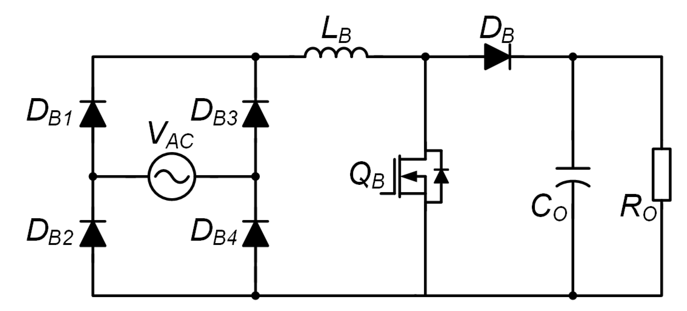
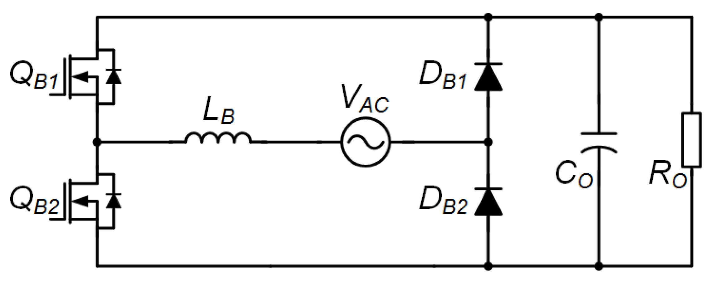
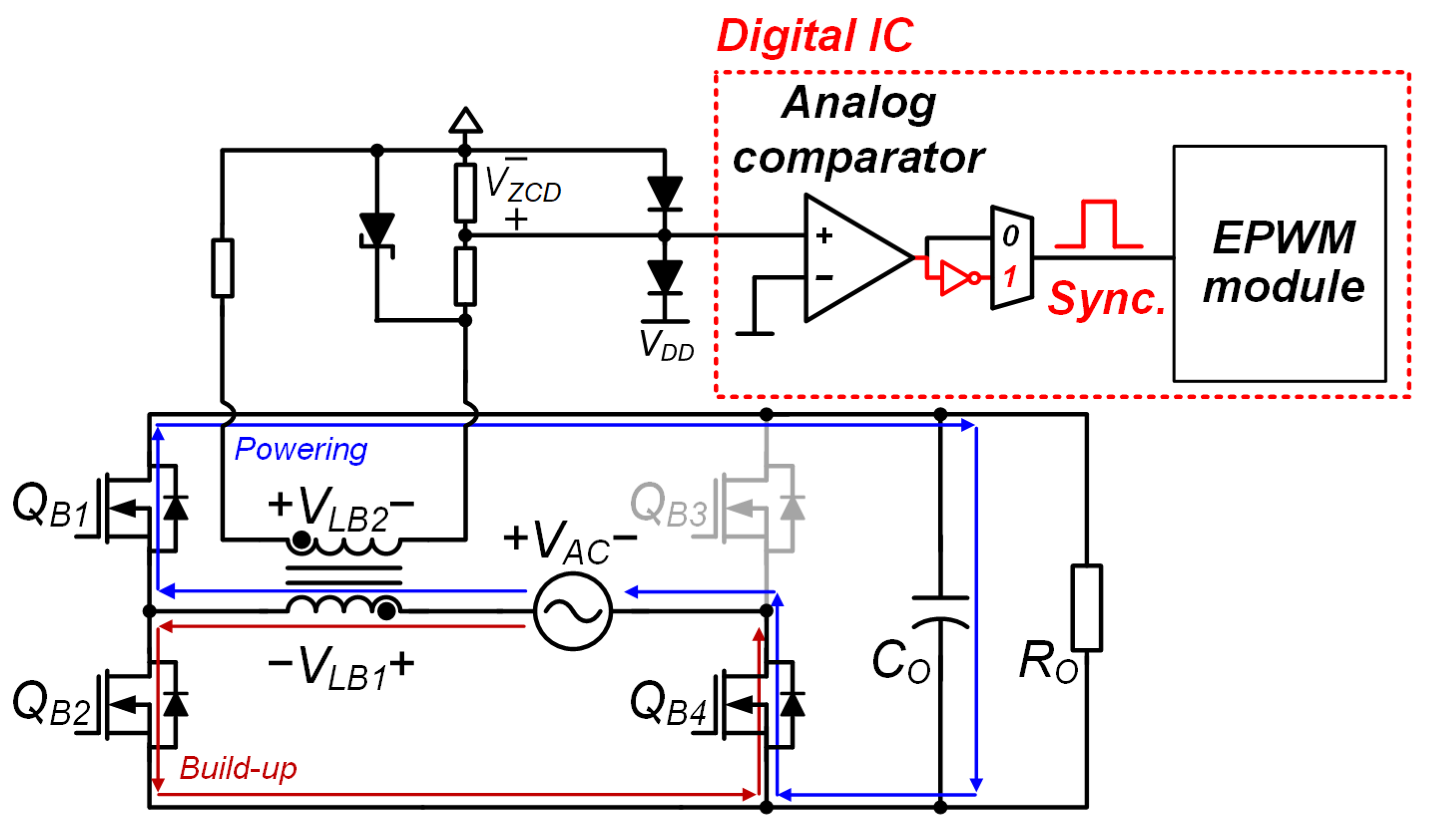
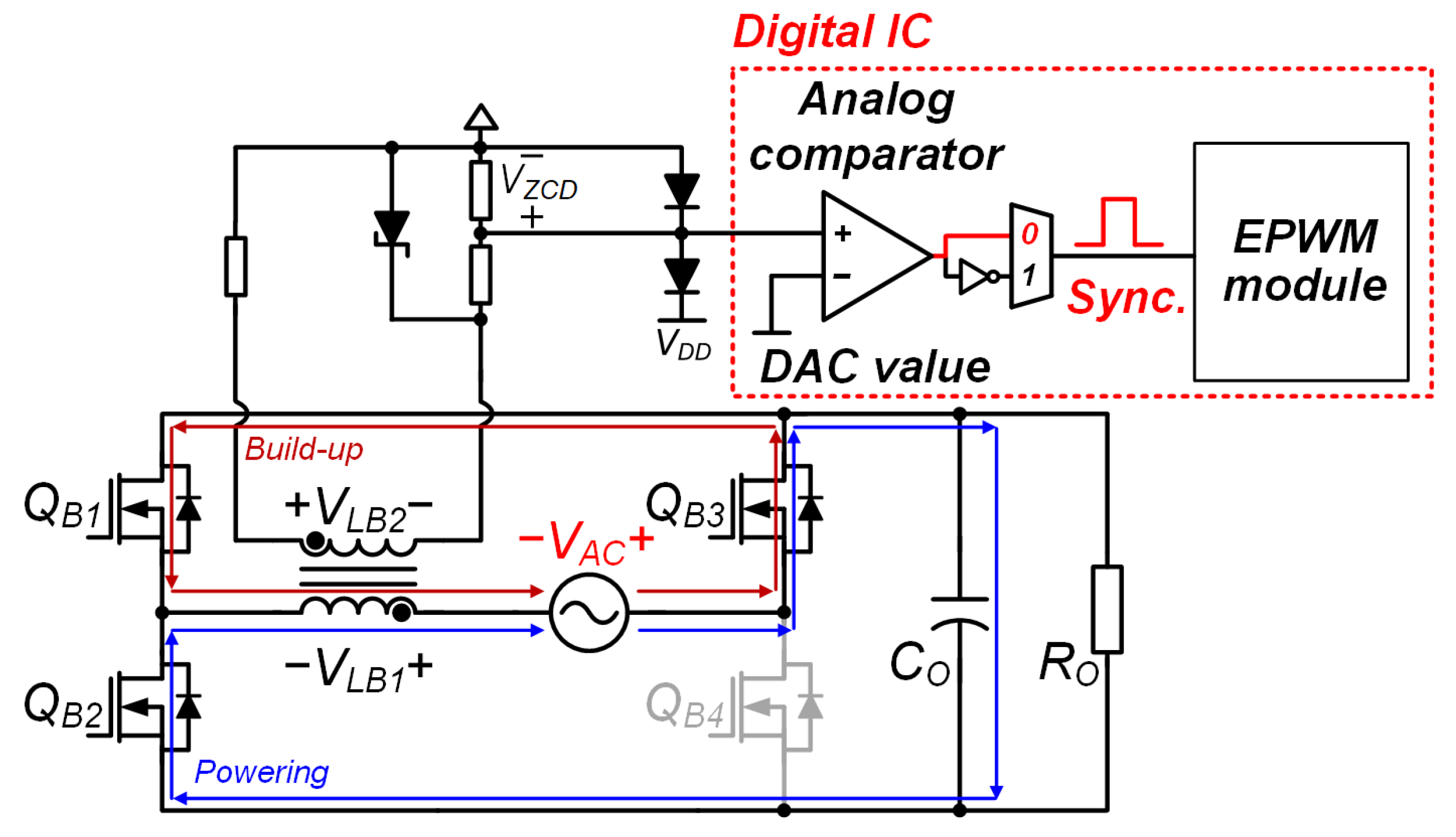
2. Basic Structure of the Digital Totem-Pole Bridgeless CRM Boost PFC Converter

The key operation of the CRM boost converter is to turn on the switch using valley switching. To achieve this, a voltage of boost inductor is generally used because the timing when the valley switching occurs is the same as the timing when the polarity of the inductor voltage is changed [26,27]. Similar to Figure 3, the inductor voltage is simply sensed with the ZCD circuit, as shown in Figure 6. As shown in figure, inductor voltage VLB1 is sensed, and it is transferred as VLB2, which makes VZCD. After the peripheral circuit is configured, the internal functions of the DSP should be set up according to the main sequence depicted in Figure 7. As shown in figure, VZCD enters the internal analog comparator of the DSP, and it is compared to the DAC value. The DAC value determines the timing when the VZCD becomes low. A low DAC value detects the timing more precisely, but it is vulnerable to a noise problem.
The output of the comparator is depicted as Comp_out, and it is synchronized with VZCD. When Comp_out occurs, a user can select the polarity between Comp_out and its inverted signal Comp_out(inverted). In a positive input cycle, Comp_out(inverted) is selected, and it is transferred to the EPWM module to make a gate signal. In the EPWM module, the DCEVT.sync signal occurs when Comp_out(inverted) becomes high, and it resets a time-base counter (EPWM_TBCTR), resulting in the turning-on of the gate signal at zero current.
In the case of a negative cycle of the input source, the role of the QB1 and QB2 are changed since input polarity is changed, as shown in Figure 8. In addition, the VLB shown in Figure 9 is the reverse of the VLB shown in Figure 7. Therefore, in a negative cycle, the Comp_out signal should not be reversed to make a trigger signal. This is easily possible by setting-up an analog comparator module. The next sequences are the same with the positive cycle. When the Comp_out signal becomes high, the DCEVT.sync signal occurs, which is used as a trigger, and the EPWM_TBCTR is reset. Because the overall sequence of the positive cycle and the negative cycle is similar, changing the polarity of the Comp_out signal at every 60 Hz cycle by sensing an input voltage source is all that is required. Since input voltage sensing is essential for every totem-pole bridgeless PFC, the sensing data is already in the DSP, and it can be used by DSP coding.

3. Additional Control Techniques

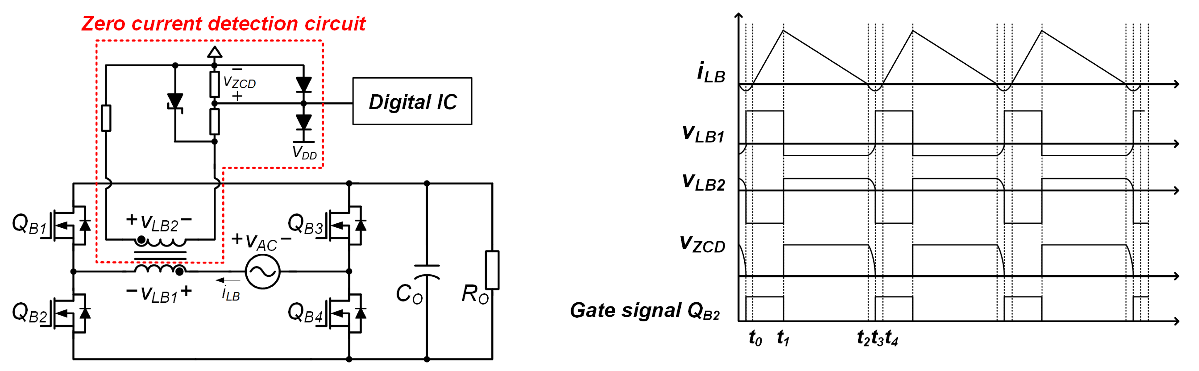
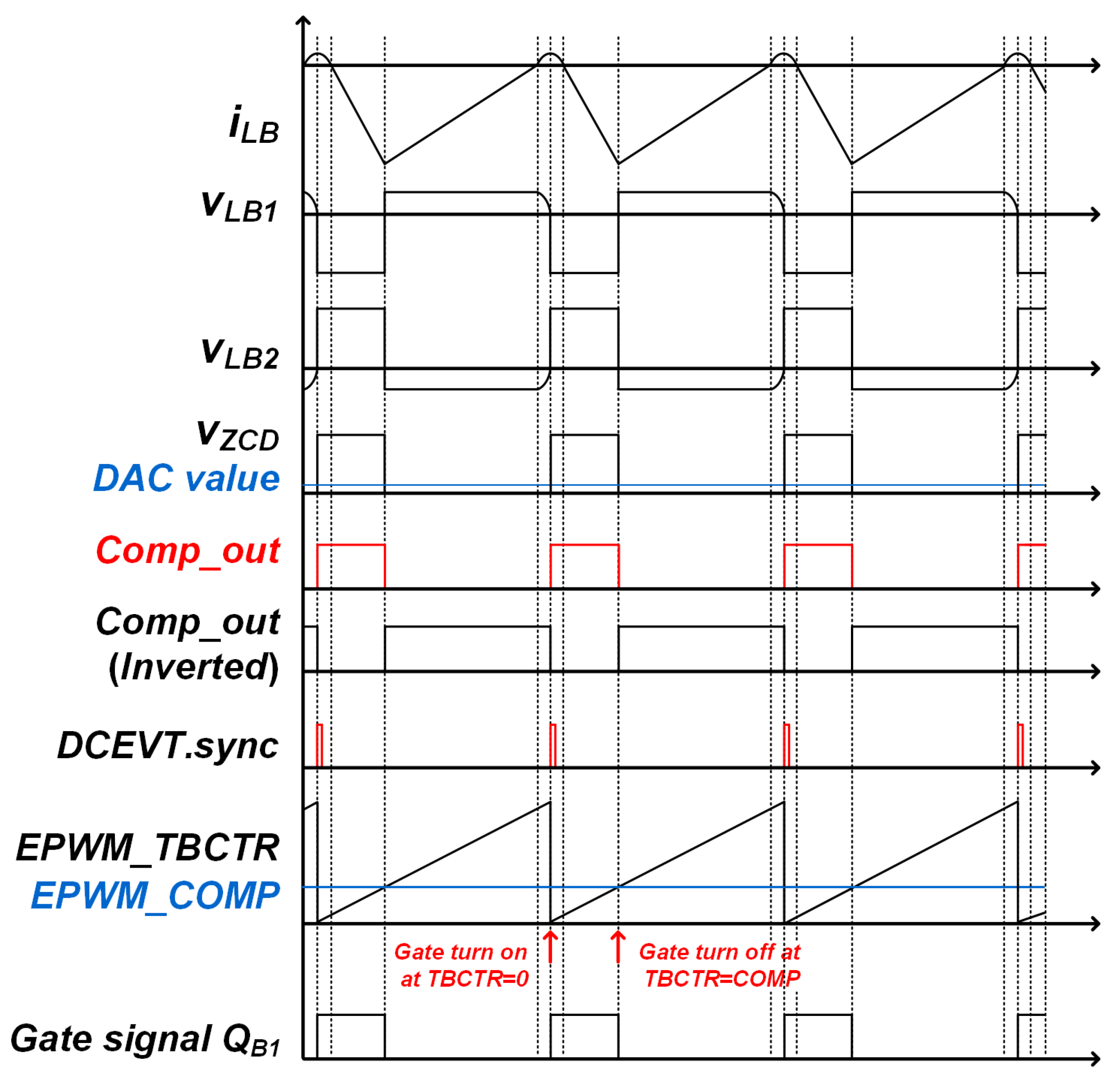
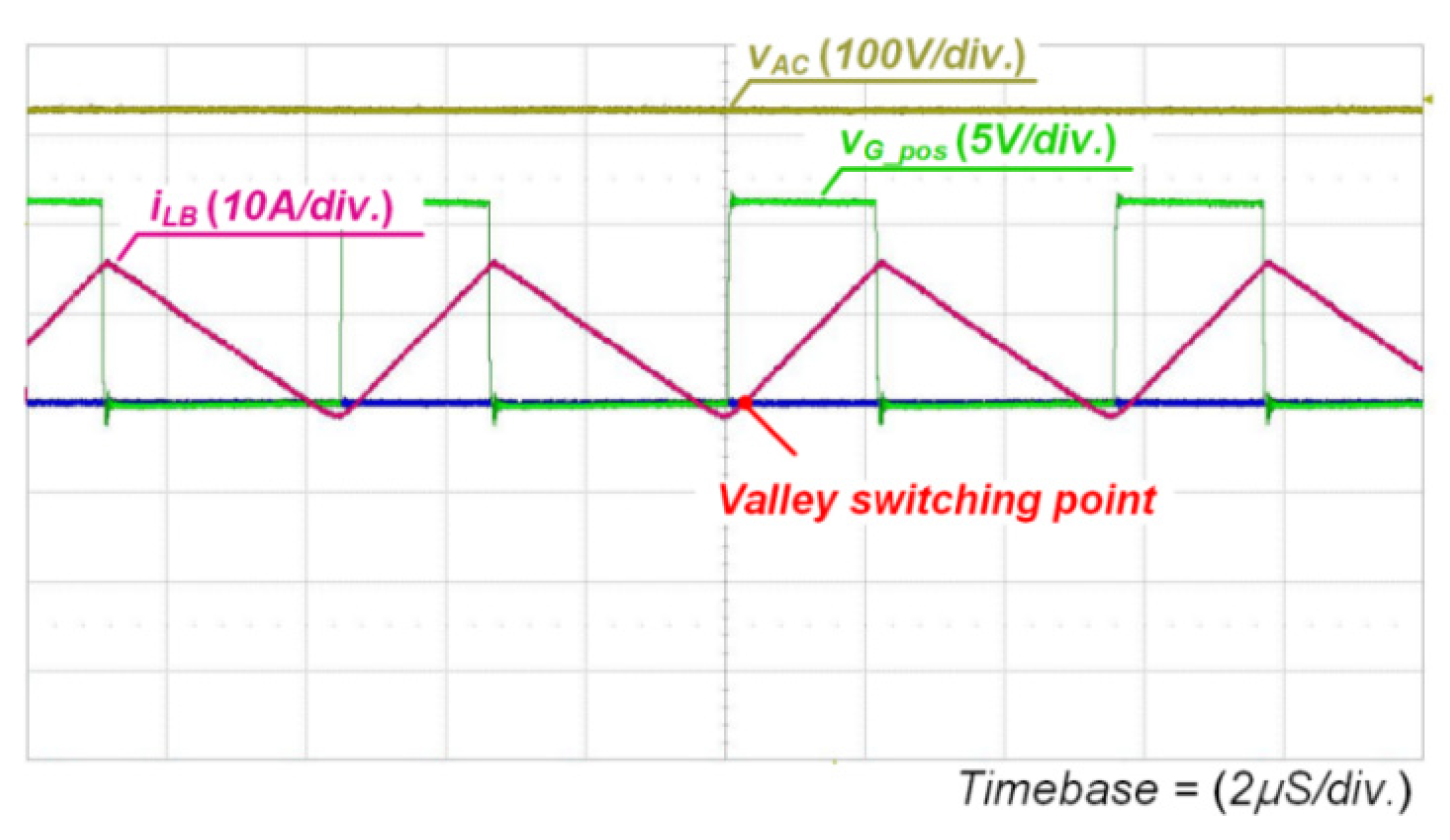
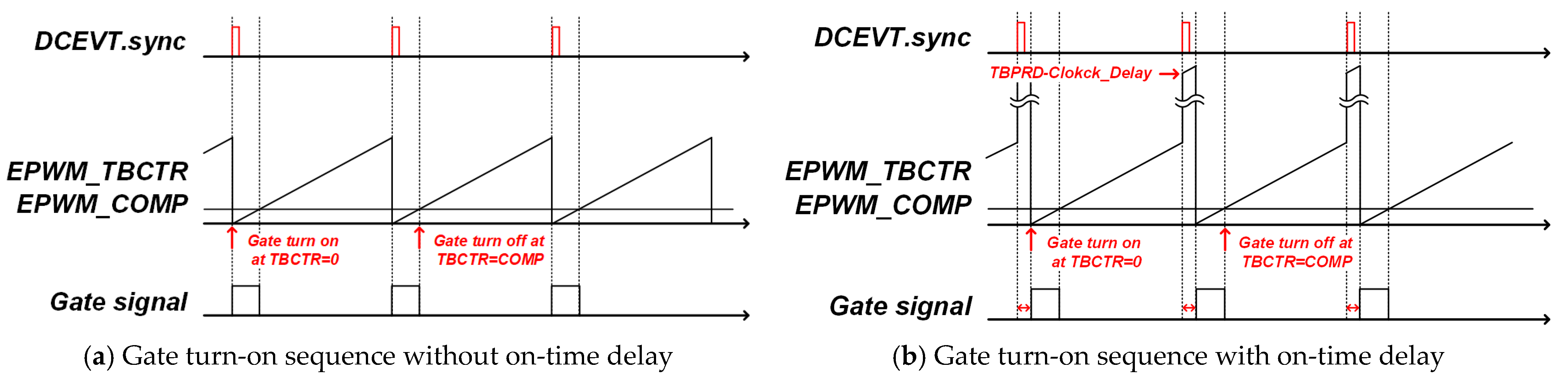
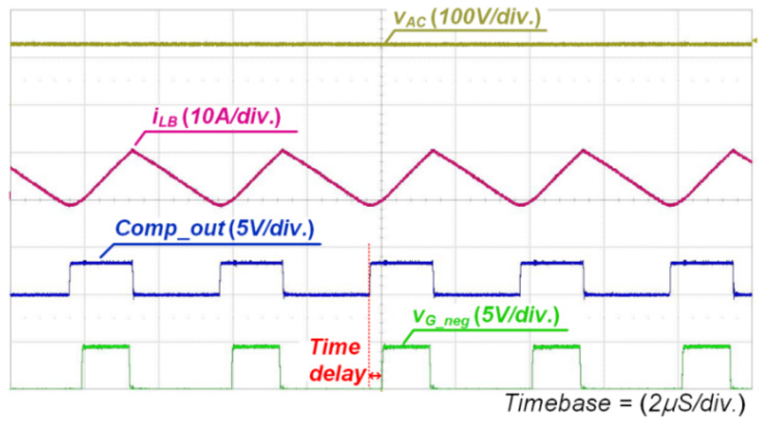
3.1. On-Time Delay Scheme for Valley Switching

With a ZCD sensing circuit and the control sequences shown in Figure 6, Figure 7, Figure 8 and Figure 9, the totem-pole bridgeless converter can be turned on with zero inductor current. However, as shown in Figure 7 and Figure 9, the gate signal is turned on at the negative peak current, which is not the exact valley switching point. This is because the trigger signal can only occur at a rising or falling edge of the signal. Therefore, with a system depicted in Figure 7 and Figure 9, the converter cannot achieve optimal valley switching. Figure 10 shows key switching waveforms of the aforementioned system.
To achieve exact valley switching, an on-time delay scheme can be applied. The key idea of the on-time delay technique is to turn-on the switch at the valley switching point by delaying the turn-on timing. Since the switch is always turned on at the negative peak current, the time remaining to the valley switching point can be calculated by using a resonant period. The resonance occurs between an output capacitor of the switch, junction capacitor of the diode, and the boost inductor. Supposing that an output capacitor of the switch is COSS, a junction capacitor of the diode is Cj, and the boost inductor is LB, the required delay time tdelay can be calculated as follows:
t d e l a y = 1 4 2 π L B ( C O S S + C j )
which is a quarter of the resonant period; non-linear characteristics are not considered for simple expression. In case of using the synchronous rectifier (SR) instead of the diode, Cj is replaced as COSS of the SR switch.
After calculating the tdelay using (1), the EPWM module should be set-up to apply on-time delay. In Figure 11a, which is the gate turn-on sequence used in Figure 7 and Figure 9, the EPWM_TBCTR is reset when the DCEVT.sync signal occurs. In contrast, in Figure 11b, the gate signal is turned on with the delay time even though the DCEVT.sync signal occurs. For this operation, the key point is to change the TBCTR action of the EPWM module when the DCEVT.sync signal occurs.
To accomplish the optimal valley switching of the switch, a time-based period (TBPRD) is used to make additional on-time delays. In the digital system, the EPWM_TBCTR increases by every 1 clock time, and when it reaches the TBPRD value, it is reset. Therefore, the TBPRD decides a switching period in a fixed frequency system. But, since the CRM control changes the switching frequency every cycle, the TBPRD is not used, and the EPWM_TBCTR is reset by other actions such as DCEVT.sync in the proposed system. The TBPRD is set only to limit the minimum frequency. However, since the EPWM_TBCTR is reset when it reaches the TBPRD, it can be used to control the EPWM_TBCTR.
In the system depicted in Figure 11a, which is the result of Figure 7 and Figure 9, when the DCEVT.sync signal occurs, the EPWM_TBCTR is reset, and the gate signal is turned on. However, in the new system shown in Figure 11b, when the DCEVT.sync occurs, the EPWM_TBCTR is not reset, and it goes to near the TBPRD value. The exact value it reaches is calculated as TBPRD-Clock_Dealy. Since the EPWM_TBCTR increases by one every one clock time of the DSP, it will reach the TBPRD after Clock_Delay * clock time, which causes the EPWM_TBCTR to be reset. For example, if the clock frequency is 200 MHz in the DSP, 1 clock time is 5 ns. Therefore, if the required on-time delay is 100 ns, the EPWM_TBCTR value should jump to TBPRD-20 when DCEVT.sync occurs. Then, after 20 clock cycles, the EPWM_TBCTR reaches the TBPRD, and the gate signal is turned on. Supposing that the value for additional on-time delay is Clock_Delay, it can be calculated as the following equation:
C l o c k _ D e l a y = t d e l a y / t c l o c k
where the tdelay is calculated with (1), and tclock is calculated with the clock frequency of the DSP.
Figure 12 shows key waveforms with the on-time delay scheme. As shown in figure, the Comp_out signal occurs at the negative peak current of the boost inductor, same as the previous method. However, although the Comp_out signal occurs, the gate signal is not turned on at that time. After that, the gate signal occurs after the time delay calculated by Equation (1), which is a quarter of the resonance time. As a result, the gate signal is turned on when the inductor current iLB becomes zero. If the gate signal is turned on before iLB is zero, it will waste energy for valley switching, and if the gate signal is turned on after iLB is larger than zero, it will also decrease the energy. Therefore, the optimal valley switching point is when iLB is exactly zero, as shown in Figure 9.

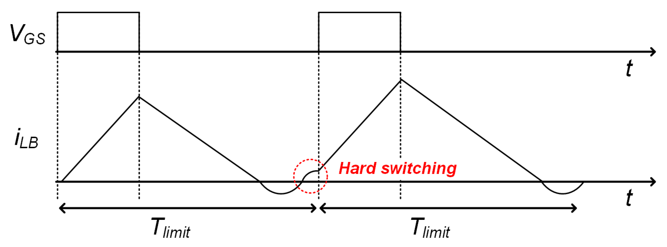
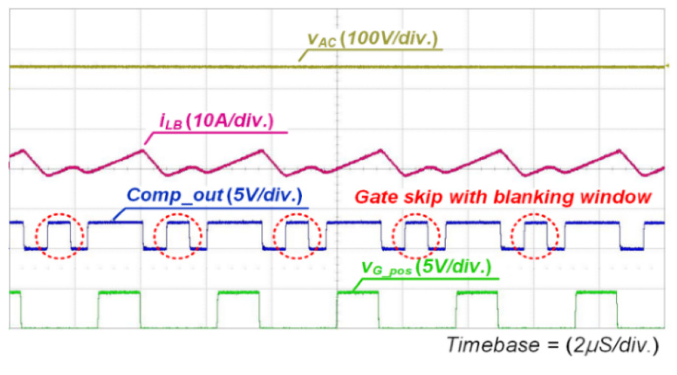
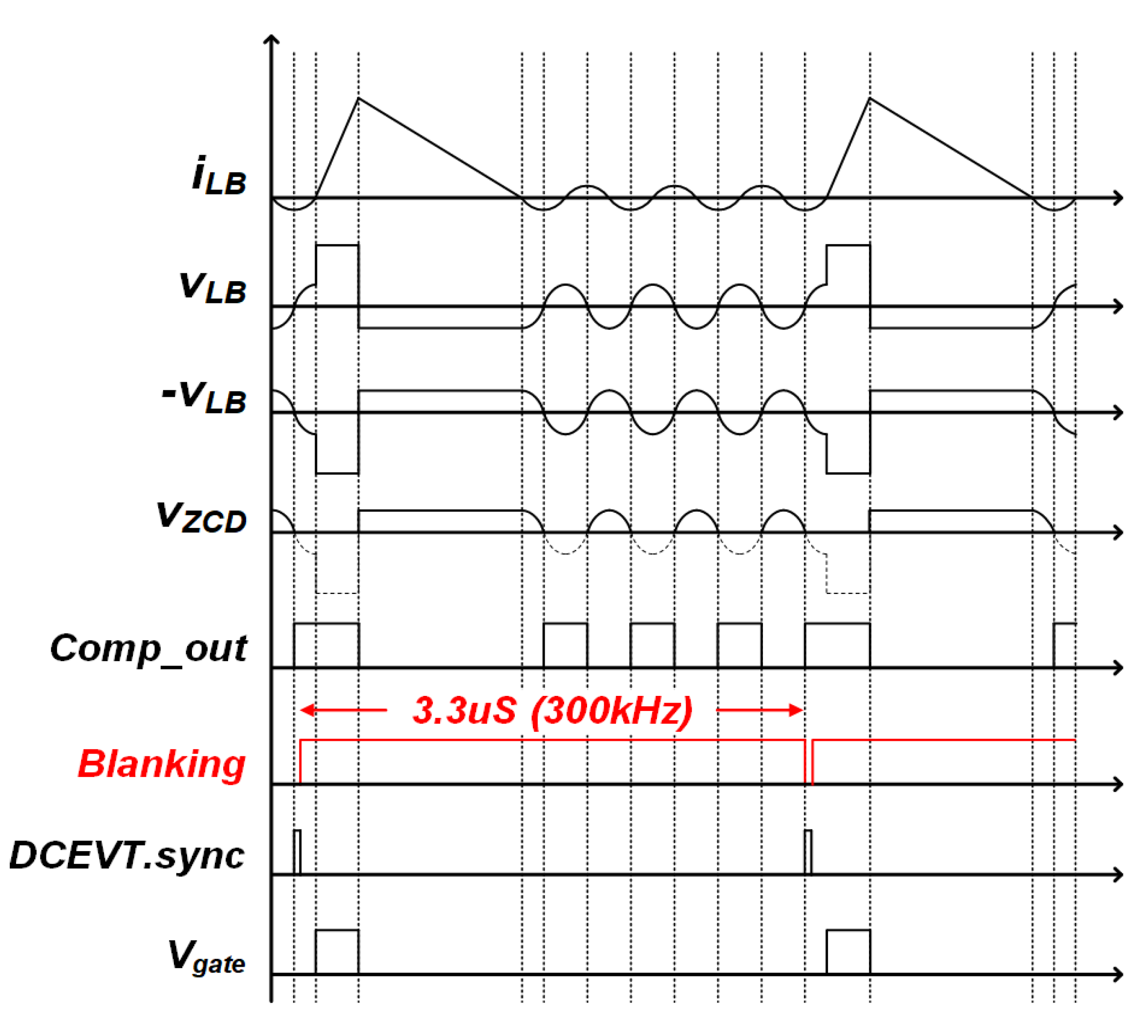
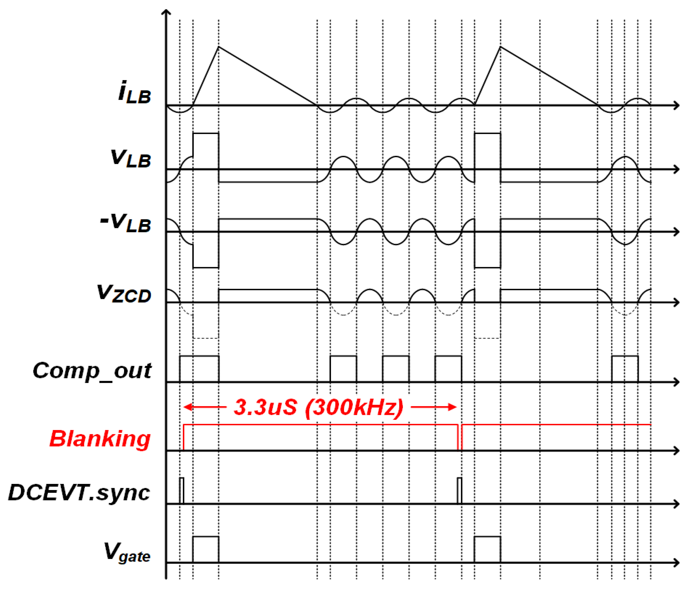
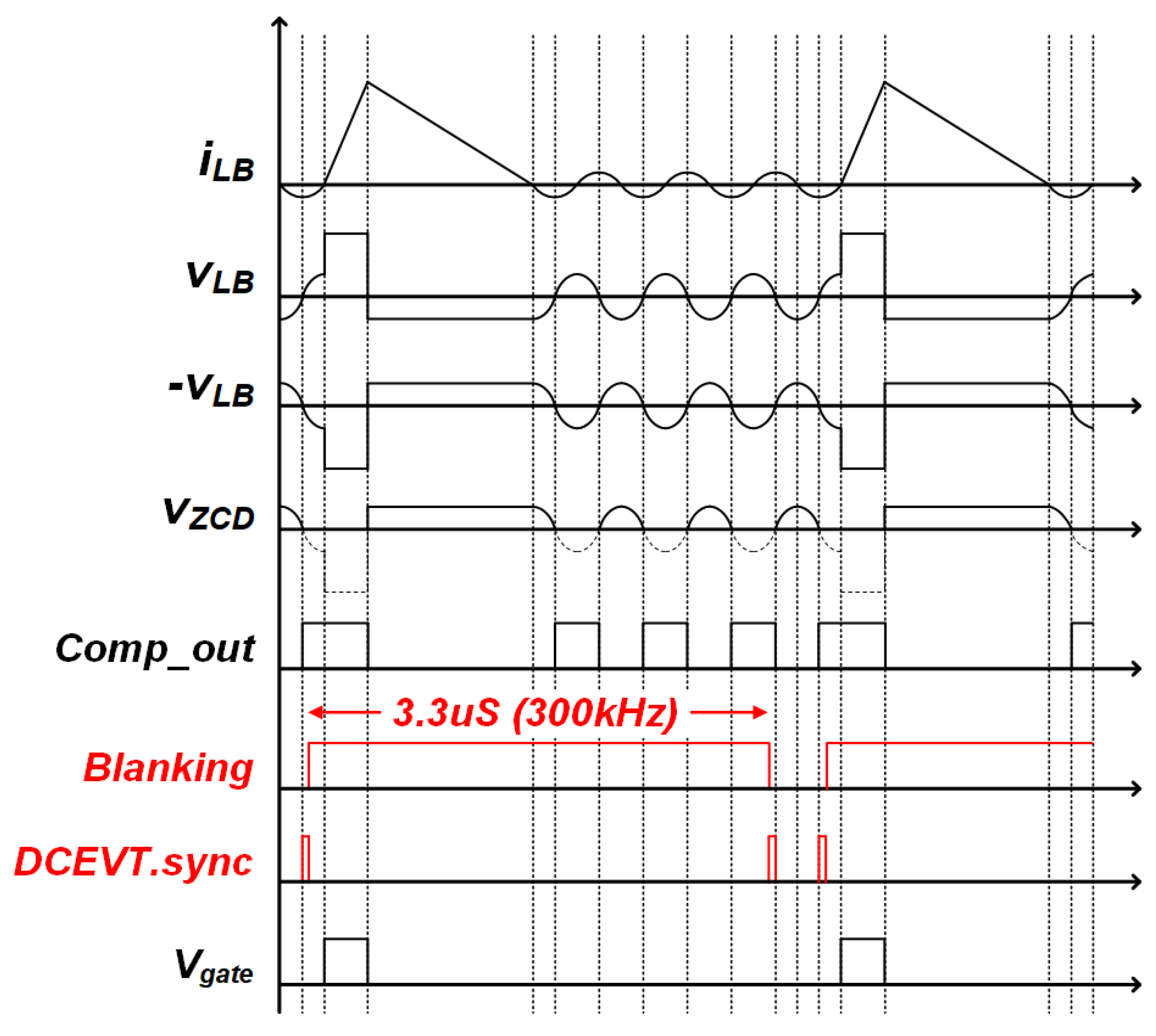
3.2. Maximum Frequency Limitation Scheme

In the CRM control, a boost converter operates with a constant on-time of the switch while the off-time of the switch varies according to the input average voltage. As a result, the CRM boost PFC converter has a variable frequency, as shown in Figure 13 [28,29]. However, since the input voltage is very low near the zero-crossing area, the ripple current of the boost inductor becomes very small, and the off-time of the switch becomes very short. As a result, the CRM boost PFC converter has a very high frequency near zero input voltage, and it is necessary to limit the maximum frequency.
To implement the maximum frequency limitation with a previous control sequence, a blanking window module can be adopted. In the system up to this point, the DCEVT.sync signal occurs when the Comp_out signal occurs. But by applying the blanking window, although the Comp_out signal occurs, the DCEVT.sync signal does not occur within the blanking window. Supposing that if the size of the blanking window is 3.3 uS, the DCEVT.sync signal never occurs during this time even though the Comp_out signal has a rising edge. As a result, EPWM_TBCTR does not reset during the blanking time, and the switch is not turned on. This limits the maximum switching frequency as 1/3.3 uS.
Figure 14 shows the key waveforms with a maximum frequency limitation scheme using the blanking window function. As shown in figure, even though the Comp_out signal occurs as iLB becomes zero, the gate signal is not turned on within blanking time. Therefore, the maximum frequency can be set-up using the blanking time.
However, when the blanking window is applied, there is a possibility to operate with a hard switching of the switch. Figure 15 shows key waveforms when the blanking window is applied. As mentioned before, although the Comp_out signal occurs, it does not cause the DCEVT.sync signal within the blanking window, which is set-up as 3.3 uS in this study. If the Comp_out signal occurs right after the blanking window is ended, as shown in figure, it transfers a trigger to the DCEVT.sync signal, and the gate signal is turned on with an optimal valley switching point.
In contrast, Figure 16 shows the key waveforms when the switch is turned on with hard switching. Compared with Figure 15, the blanking window ends while the Comp_out signal is still high. Because the blanking window ends and the Comp_out signal is high, it causes the DCEVT.sync signal, although it is not a valley switching point. As a result, it causes hard switching, which increases switching loss.
To solve the problem, an Edge filter of the EPWM module can be used. The Edge filter counts the number of occurrences of the trigger signal. If count of the Edge filter is set-up as 2, the EPWM module ignores first DCEVT.sync signal, and the switch is turned on with second DCEVT.sync. Since the possibility of the hard switching happens only at the first DCEVT.sync trigger, the valley switching can be achieved always by ignoring first DEVET.sync signal occurs after the blanking window.
Figure 17 shows the key waveforms using the Edge filter after blanking window. As shown in figure, although the Comp_out signal is high, DCEVT.sync signal is not occurs during blanking time. And, when the blanking time is ended while the Comp_out signal is high, the DCEVT.sync signal occurs. However, since the Edge filter ignores first DCEVT.sync signal, the gate signal is not turned on. After that, when the Comp_out signal occurs, it causes second DCEVT.sync signal, and the gate signal is turned on with optimal valley switching point. Consequently, the CRM boost PFC converter can limit the maximum frequency while maintains the valley switching.
Figure 18 shows the key waveforms of the CRM boost converter in near zero voltage of the input. Because the CRM boost converter has high frequency near zero voltage, the maximum frequency limitation is applied with 300 kHz. But, as shown in Figure 18a, the switch is turned on with hard switching since the DCEVT.sync signal doesn’t occur at the rising edge of the Comp_out signal due to blanking window. On the other hand, Figure 18b shows the valley switching operation although the DCEVT.sync signal occurs in the wrong point due to the end time of the blanking window function. This is because the Edge filter function filters the first DCEVT.sync signal to remove the possibility of hard switching.

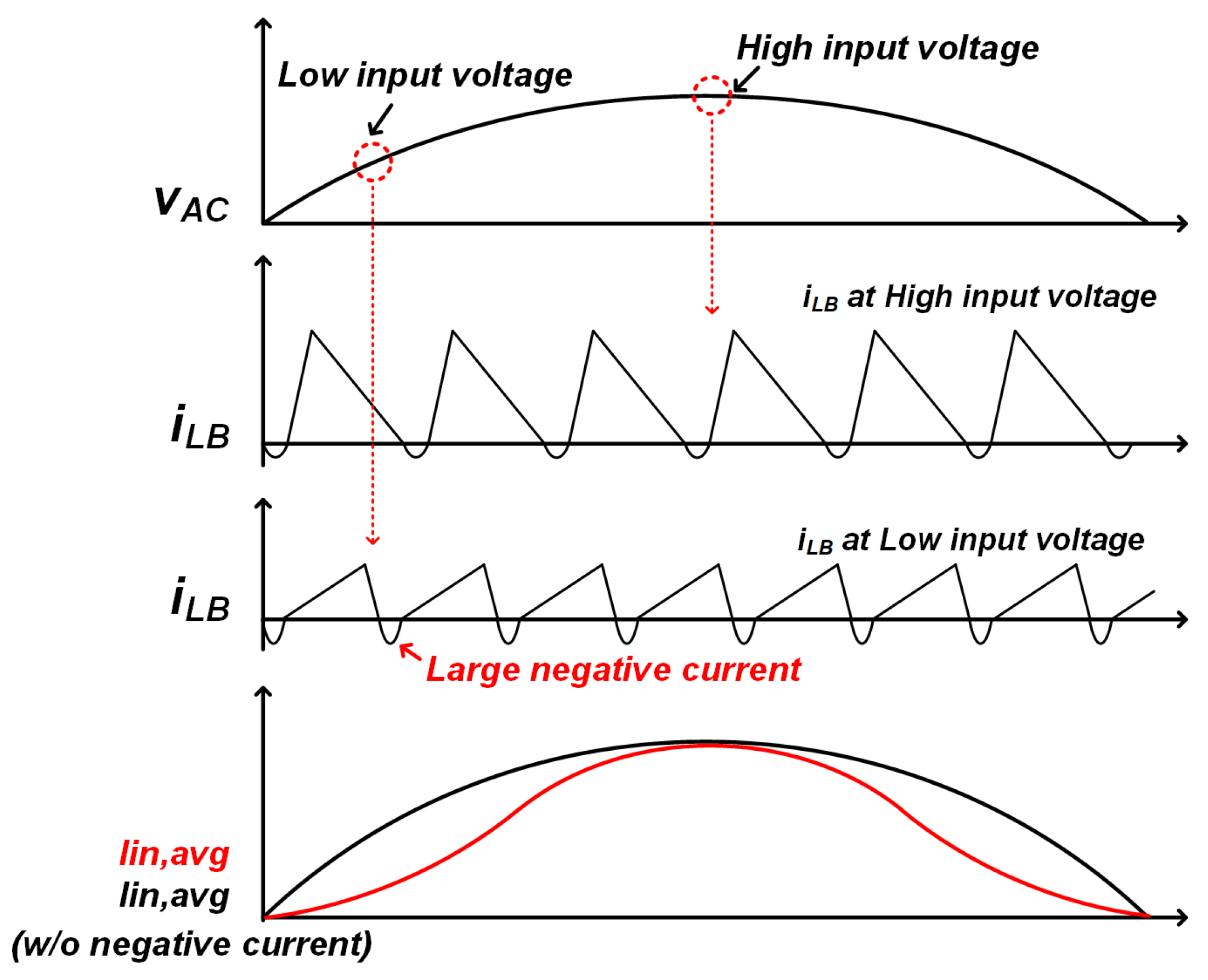
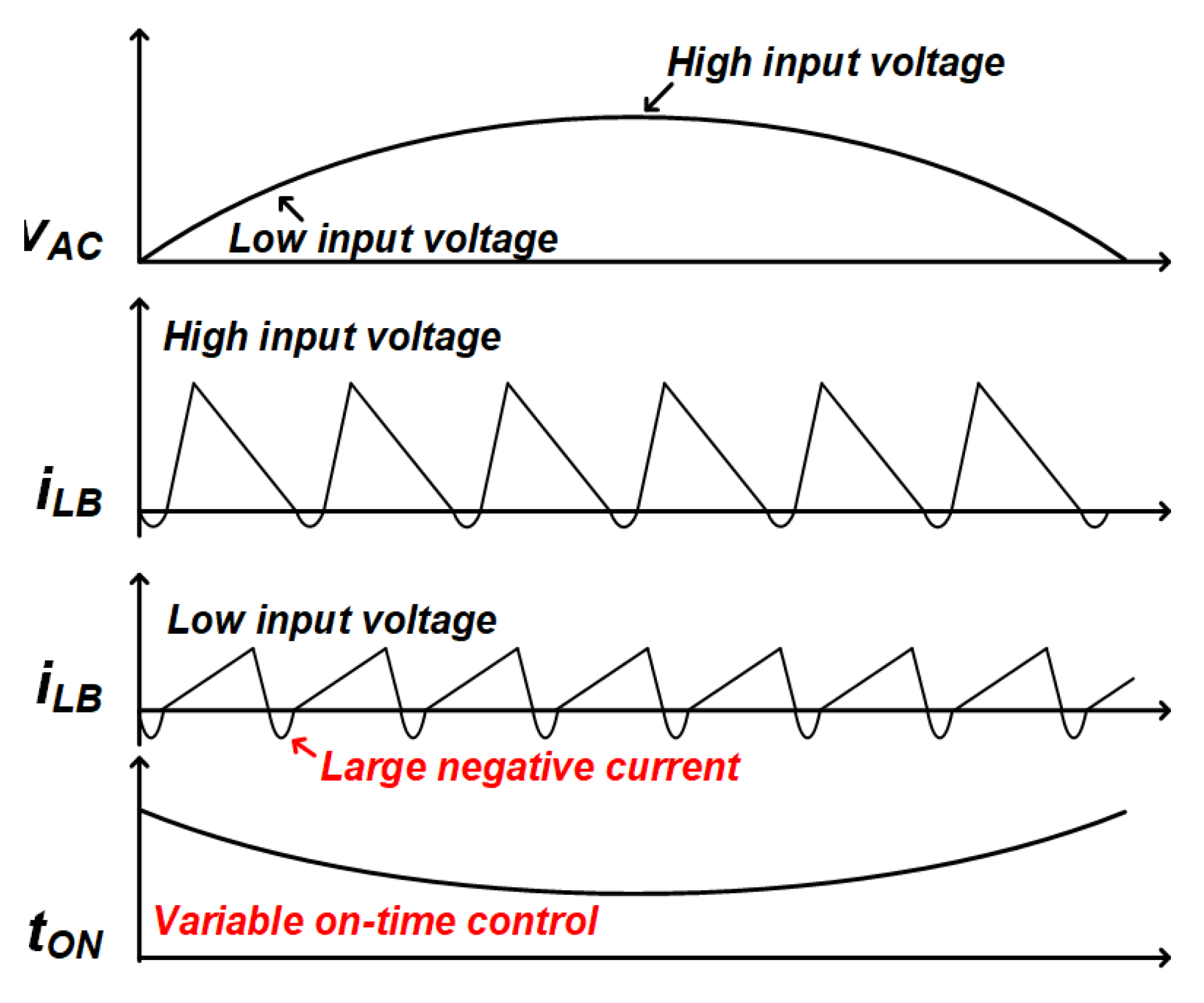
3.3. Additional On-Time Control

One of the most important factors of the PFC stage is PF. Since the totem-pole bridgeless CRM boost PFC converter is used for the PFC stage, it also has to achieve a high PF. However, the CRM-based boost converter always has low PF problems under light-load conditions due to high THD.
This problem occurs by reverse current of the boost inductor which used to valley switching of the switch. As shown in Figure 19, the input AC voltage varies with the 60 Hz cycle, and the input voltage of the PFC converter also varies at 60 Hz. But compared with the inductor current at a high input voltage, the inductor current at a low input voltage has large negative current. This is because the initial condition of the resonance is larger at low input voltage. In addition, since the average current of the boost inductor is smaller at low input voltage, the proportion of the negative current become much larger at the low input voltage than it does at the high input voltage condition. As a result, the average input current becomes smaller near the low input voltage, resulting in distortion of the sine wave.
Figure 20 shows the inductor current iLB and average current Iin according to the input voltage VAC. As shown in the figure, Iin has a distorted sine wave, especially a low average current near the low input voltage condition, even though the peak current of iLB is shaped well as input voltage.
To improve this problem, an additional on-time control scheme can be applied. Compared to a conventional CRM control, which uses a constant on-time control, a variable on-time control is adopted according to a 60 Hz AC input voltage. As shown in Figure 19, it increases on-time near low input voltage, and it reduces on-time near the high input voltage condition. Therefore, the average current near the low input voltage increases, and the average current near the high input voltage decreases. A reference signal for the variable on-time control can be implemented by adding a reverse sine shape to the conventional reference signal. To make the reverse sine shape, a scaled input voltage signal can be used. Since the average value of the reference signal should not be changed, the reverse sine wave has zero average value. Supposing that the input voltage is αVmsin(t), where α is the scale down factor, the reverse sine wave with zero average value can be calculated as follows:
0 π 2 x α V m sin t d t = 0
x = 2 α V m π
By adopting the additional reference signal using (4), the average input current has a lower THD value. Figure 21 shows the modified input current signal using the additional on-time scheme. As shown in figure, the distortion of the input current reduced significantly under the same power condition, indicating a low THD value. As a result, by adopting the additional on-time scheme, the CRM boost PFC converter achieves high PF with low THD.

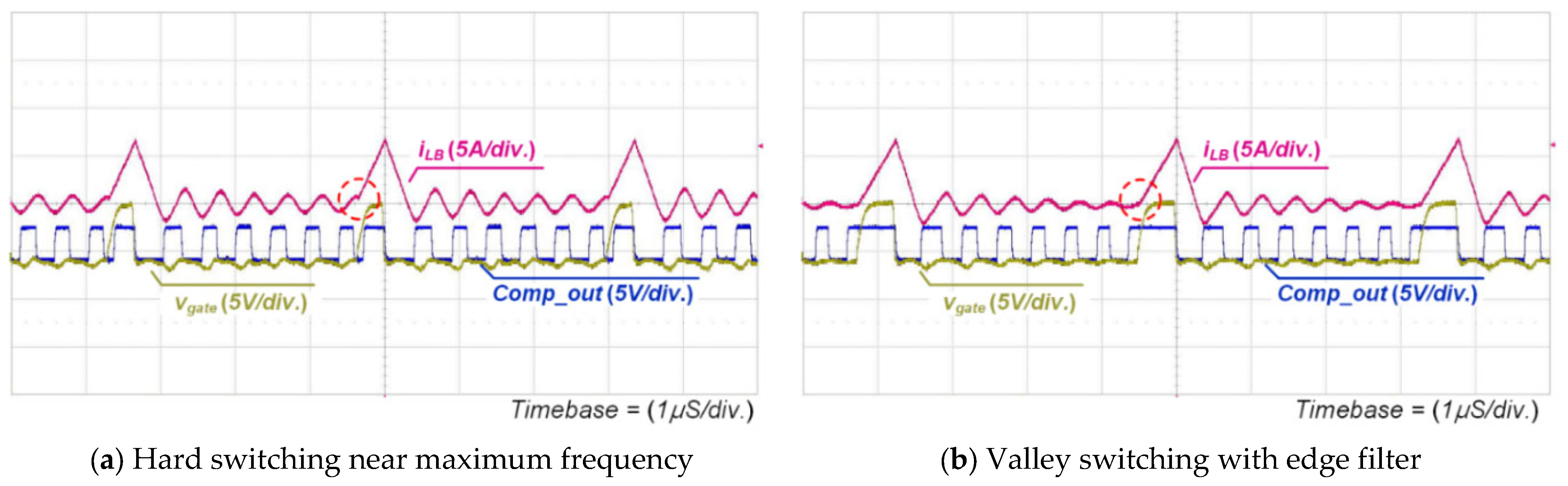
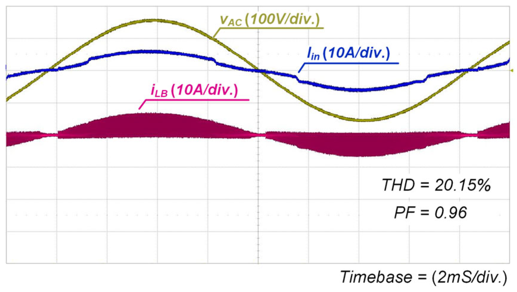
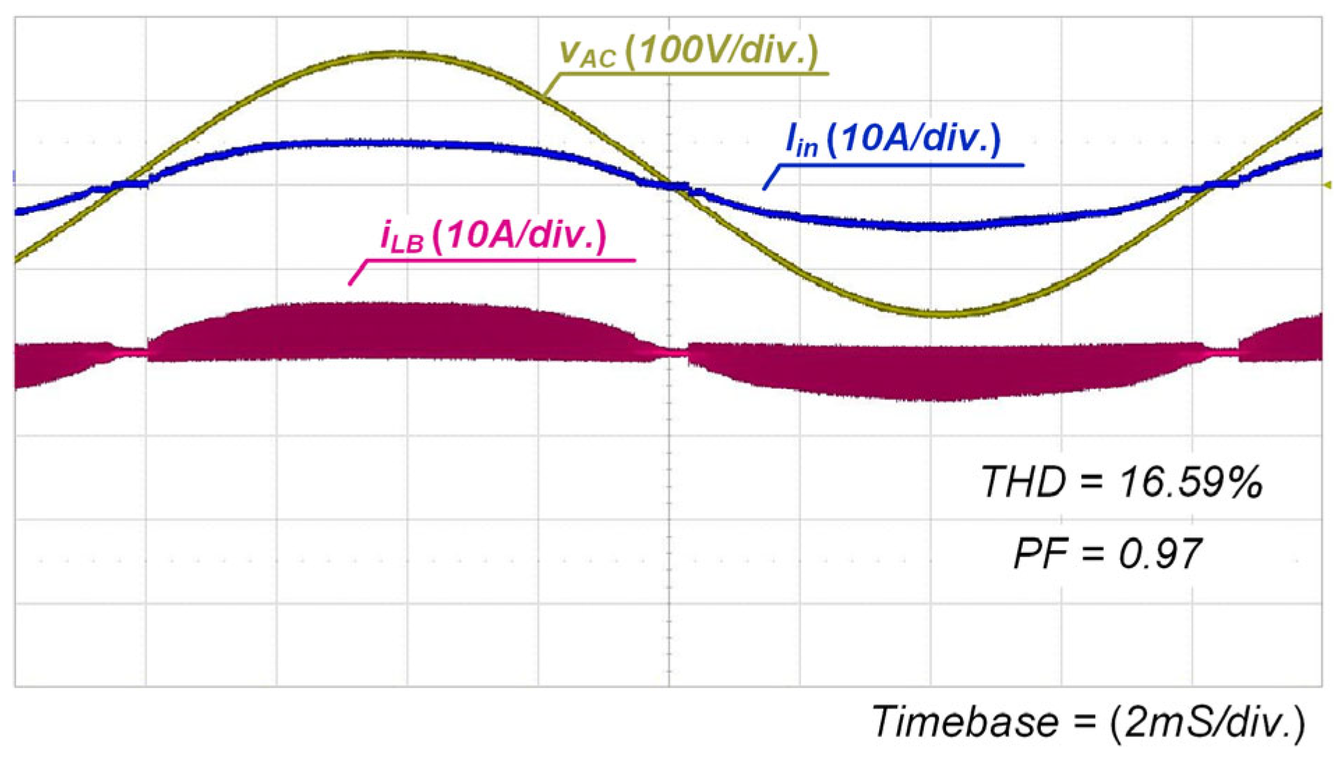
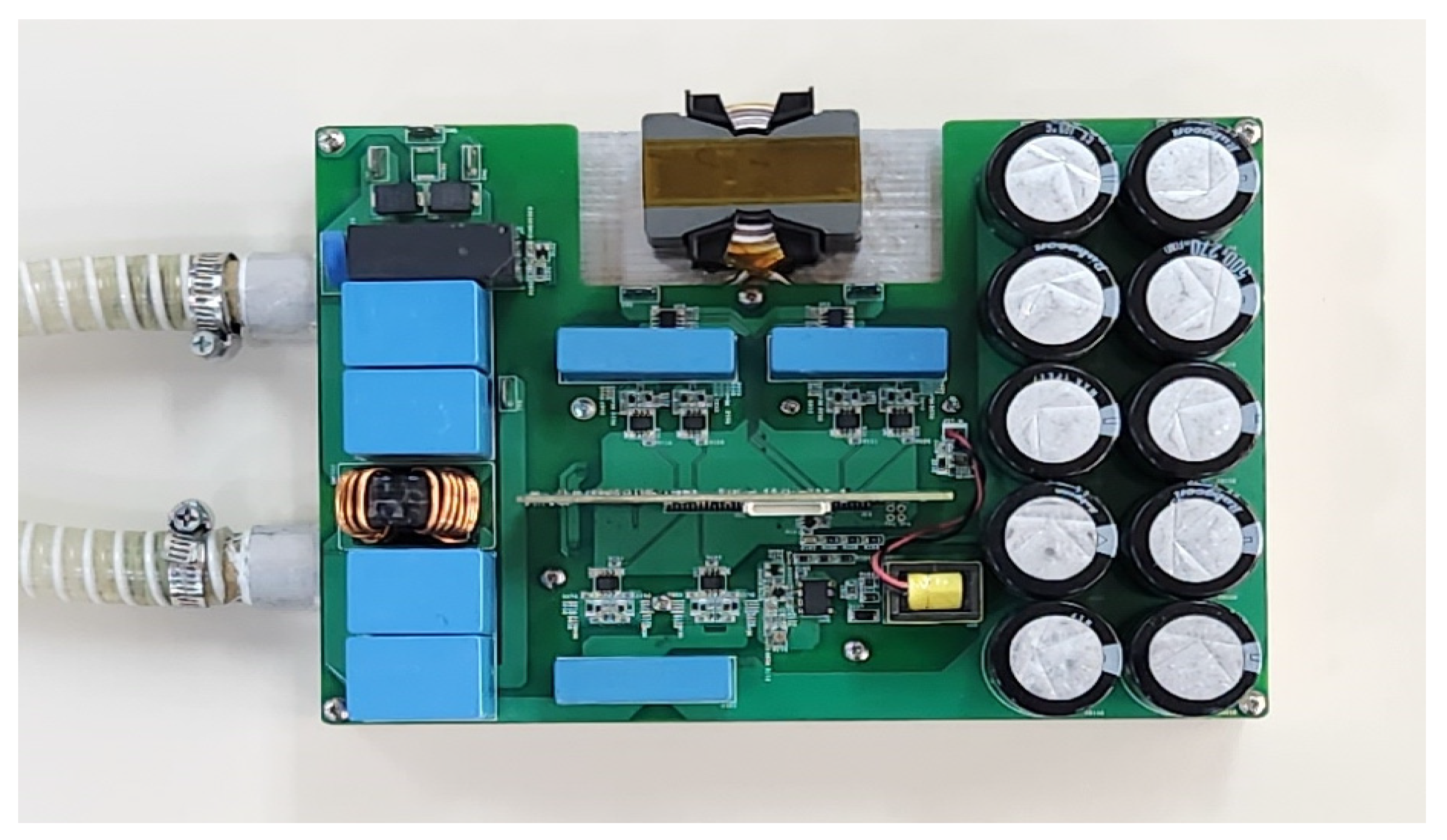
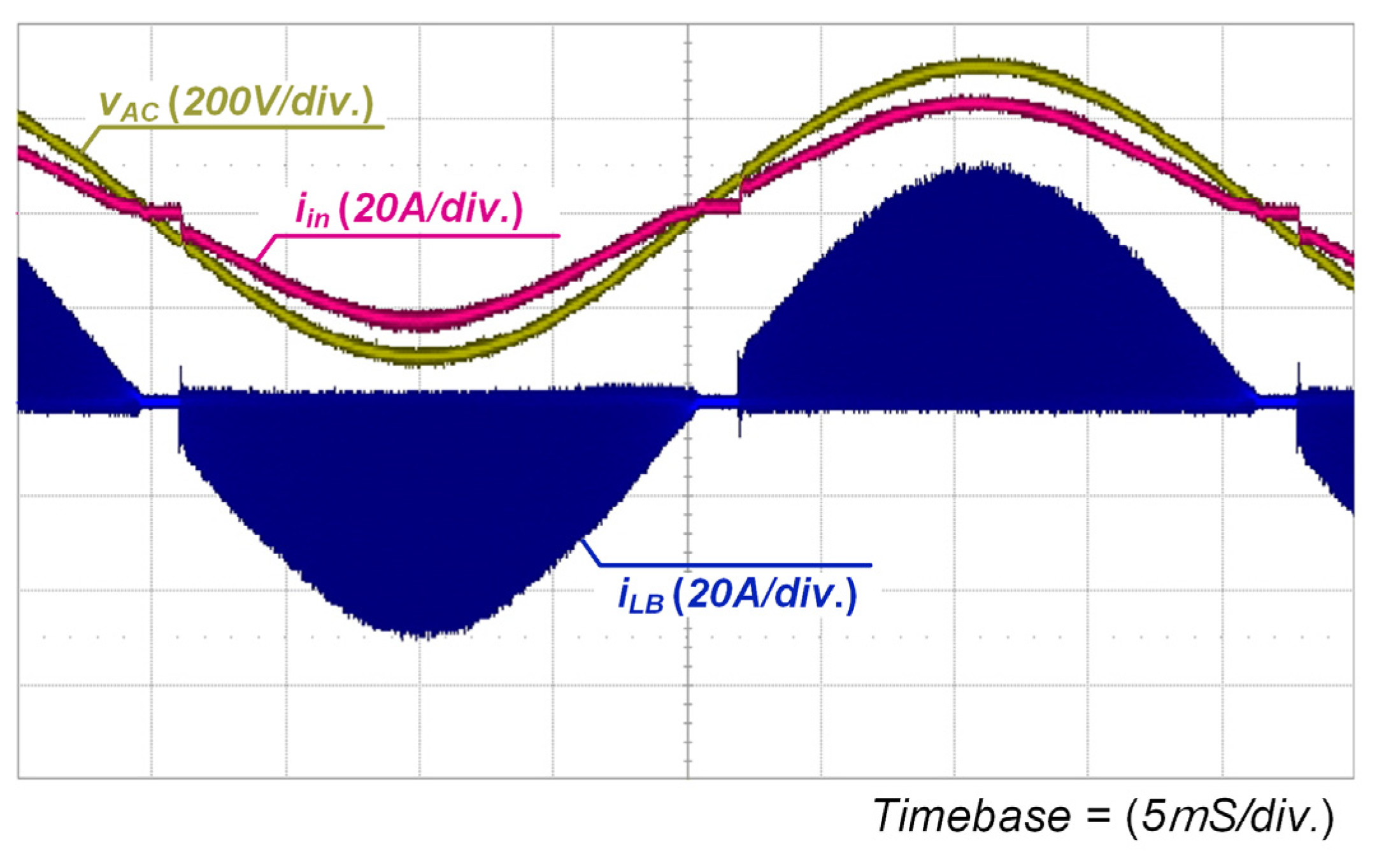
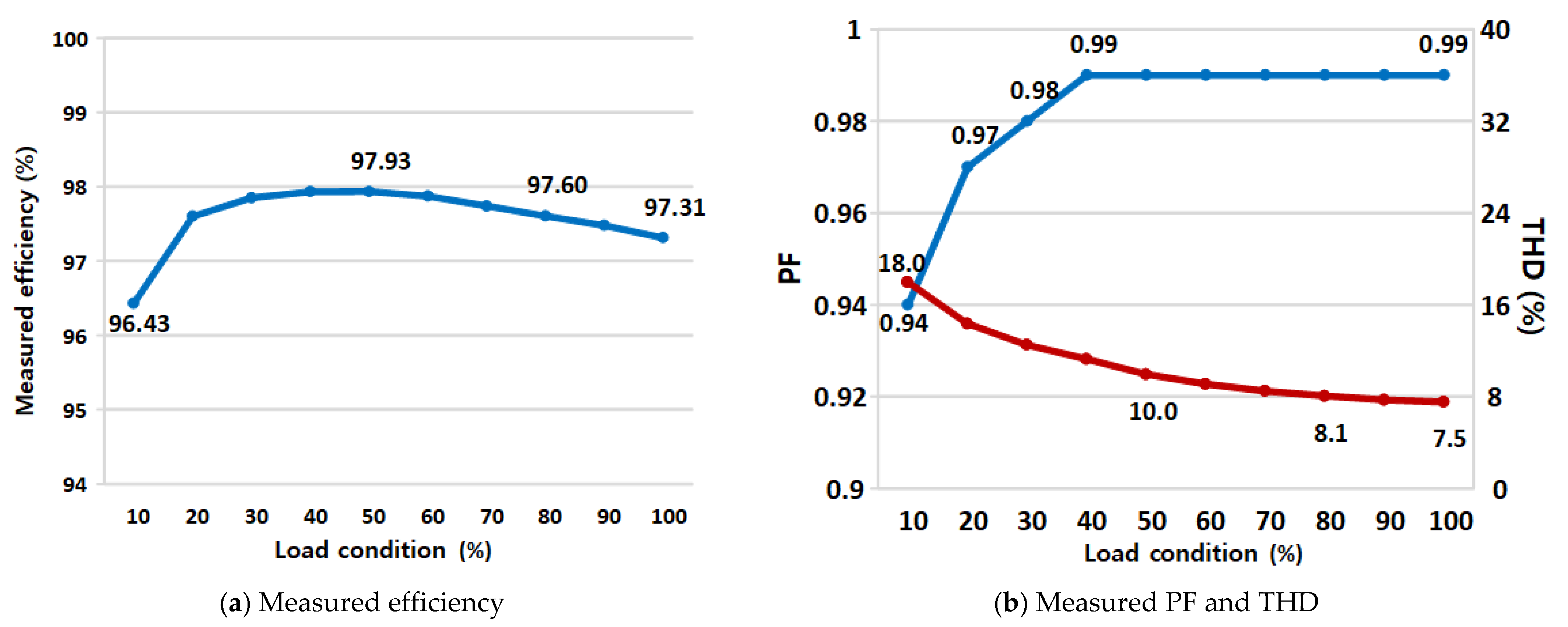
4. Experimental Results

The effectiveness and feasibility of the digital totem-pole bridgeless CRM boost PFC converter was verified using 90–264 VAC input and 450 V/3.3 kW output specifications. Detailed design parameters are listed in Table 1. To implement the digital system, a TMS320F28377 from TI was used with peripheral circuits. The GS66516T was used for switches QB1 and QB2 with a 300 kHz maximum switching frequency. The bridge diode LL25XB60 was used for the 60 Hz line frequency diodes DB1 and DB2. Lastly, the boost inductor was designed to use PQ5030 with a 0.1Φ × 300 strands litz wire considering the maximum flux density and current density. The efficiency, PF, and THD were measured with a Yokogawa WT1800 high-accuracy power analyzer. Table 2 shows comparisons between reference papers. Compared with the reference papers, the proposed system does not require auxiliary components.
Figure 22 shows the prototype converters based on Table 1. It has a water-cooling structure since it transfers high power, and the heat of the magnetic components and all switches are dissipated with the water cooling. The daughter DSP board is inserted vertically to minimize the noises from power lines.
Figure 23 shows the key waveforms of the totem-pole bridgeless CRM boost PFC converter at 220 VAC input and 450 V/3.3 kW output specifications. As shown in figure, inductor current iLB operates with critical mode to achieve valley switching. In addition, by adopting the additional on-time scheme, the input average current iin has low THD compared to the conventional CRM system.
Figure 24 shows the measured efficiency, PF, and THD under the entire load condition. As shown in Figure 24a, the maximum efficiency is around 98% under the half-load condition. It is possible to improve the efficiency of this system by decreasing the switching frequency, but since the low frequency requires a large-volume system, a 100–300 kHz switching frequency is applied, considering the size of the magnetic components. Figure 24b shows the PF and THD of the converter. As shown in the figure, both PF and THD are better under the heavy-load condition. The reason for this is that the phase-leading current of input capacitor filter degrades the PF under light-load conditions [30]. The effect of the phase-leading current becomes weak under the heavy-load condition.

5. Conclusions

In this paper, a digital CRM totem-pole bridgeless boost PFC converter is proposed with various additional techniques to improve the performance of the system. The CRM totem-pole bridgeless boost PFC converter is very attractive for topologies in high-power applications since it has a small number of components compared to a conventional boost PFC converter. However, it has many limitations of CRM operation, such as implementation of valley switching, hard-switching possibility with frequency limitation, and a current distortion near zero input voltage. To solve these problems, many studies have proposed various ideas, but most of them require additional components to implement the idea. On the other hand, this study achieves the aforementioned functions without any additional components, using the TI DSP and control schemes. As a result, the proposed system achieved high efficiency, high PF, and low THD using various techniques such as on-time delay, maximum frequency limitation, blanking window, edge filter, and additional on-time schemes. The prototype converter is verified using the 450 V/3.3 kW output specifications to target OBC. The proposed system is a good candidate for applications which require high power with high efficiency and high PF, such as electric vehicles.

Funding

This research was supported by the “Regional Innovation Strategy (RIS)” through the National Research Foundation of Korea (NRF), funded by the Ministry of Education (MOE) (2021RIS-004) and MSIT (Ministry of Science and ICT), Korea, under the ICAN (ICT Challenge and Advanced Network of HRD) program (IITP-2023-00156212), supervised by the IITP (Institute of Information & Communications Technology Planning & Evaluation).

Data Availability Statement

Data available in a publicly accessible repository.

Conflicts of Interest

The author declares no conflicts of interest.

References

  1. Zhang, L.; Wang, Y.; Wang, Z. Robust Lateral Motion Control for In-Wheel-Motor-Drive Electric Vehicles with Network Induced Delays. IEEE Trans. Veh. Technol. 2019, 68, 10585–10593. [Google Scholar] [CrossRef]
  2. Ding, X.; Wang, Z.; Zhang, L.; Wang, C. Longitudinal Vehicle Speed Estimation for Four-Wheel-Independently-Actuated Electric Vehicles Based on Multi-Sensor Fusion. IEEE Trans. Veh. Technol. 2020, 69, 12797–12806. [Google Scholar] [CrossRef]
  3. Zhang, W.; Wang, Z.; Drugge, L.; Nybacka, M. Evaluating Model Predictive Path Following and Yaw Stability Controllers for Over-Actuated Autonomous Electric Vehicles. IEEE Trans. Veh. Technol. 2020, 69, 12807–12821. [Google Scholar] [CrossRef]
  4. Zinchenko, D.; Blinov, A.; Chub, A.; Vinnikov, D.; Verbytskyi, I.; Bayhan, S. High-Efficiency Single-Stage On-Board Charger for Electrical Vehicles. IEEE Trans. Veh. Technol. 2021, 70, 12581–12592. [Google Scholar] [CrossRef]
  5. Meher, S.R.; Banerjee, S.; Vankayalapati, B.T.; Singh, R.K. A Reconfigurable On-Board Power Converter for Electric Vehicle with Reduced Switch Count. IEEE Trans. Veh. Technol. 2020, 69, 3760–3772. [Google Scholar] [CrossRef]
  6. Tong, M.; Cheng, M.; Hua, W.; Ding, S. A Single-Phase On-Board Two-Stage Integrated Battery Charger for EVs Based on a Five-Phase Hybrid-Excitation Flux-Switching Machine. IEEE Trans. Veh. Technol. 2020, 69, 3793–3804. [Google Scholar] [CrossRef]
  7. Kim, D.-H.; Lee, B.-K. Asymmetric Control Algorithm for Increasing Efficiency of Nonisolated On-Board Battery Chargers with a Single Controller. IEEE Trans. Veh. Technol. 2017, 66, 6693–6706. [Google Scholar] [CrossRef]
  8. Lee, B.-K.; Kim, J.-P.; Kim, S.-G.; Lee, J.-Y. An Isolated/Bidirectional PWM Resonant Converter for V2G(H) EV On-Board Charger. IEEE Trans. Veh. Technol. 2017, 66, 7741–7750. [Google Scholar] [CrossRef]
  9. Khaligh, A.; D’Antonio, M. Global Trends in High-Power On-Board Chargers for Electric Vehicles. IEEE Trans. Veh. Technol. 2019, 68, 3306–3324. [Google Scholar] [CrossRef]
  10. Mallik, A.; Khaligh, A. Intermediate DC-Link Capacitor Reduction in a Two-Stage Cascaded AC/DC Converter for More Electric Aircrafts. IEEE Trans. Veh. Technol. 2018, 67, 935–947. [Google Scholar] [CrossRef]
  11. Li, G.; Yang, D.; Zhou, B.; Zhang, H. A Topology-Reconfigurable LLC Resonant Converter for Wide Output Range Applications. IEEE Trans. Veh. Technol. 2022, 71, 10389–10399. [Google Scholar] [CrossRef]
  12. Mallik, A.; Lu, J.; Khaligh, A. Sliding Mode Control of Single-Phase Interleaved Totem-Pole PFC for Electric Vehicle Onboard Chargers. IEEE Trans. Veh. Technol. 2018, 67, 8100–8109. [Google Scholar] [CrossRef]
  13. Park, M.-H.; Baek, J.; Jeong, Y.; Moon, G.-W. An Interleaved Totem-Pole Bridgeless Boost PFC Converter with Soft-Switching Capability Adopting Phase-Shifting Control. IEEE Trans. Power Electron. 2019, 34, 10610–10618. [Google Scholar] [CrossRef]
  14. Amiri, P.; Eberle, W.; Gautam, D.; Botting, C. An Adaptive Method for DC Current Reduction in Totem Pole Power Factor Correction Converters. IEEE Trans. Power Electron. 2021, 36, 11900–11909. [Google Scholar] [CrossRef]
  15. LE, T.-T.; Hakim, R.M.; Choi, S. A High-Efficiency Bidirectional Single-Stage AC-DC Converter Under Wide Voltage Range for Fast Chargers. IEEE Trans. Power Electron. 2023, 38, 4945–4956. [Google Scholar] [CrossRef]
  16. Fischer, G.d.S.; Rech, C.; de Novaes, Y.R. Extensions of Leading-Edge Modulated One-Cycle Control for Totem-Pole Bridgeless Rectifiers. IEEE Trans. Power Electron. 2020, 35, 5447–5460. [Google Scholar] [CrossRef]
  17. Valipour, H.; Mahdavi, M.; Ordonez, M.; Ksiazek, P.F.; Khandekar, R.M. Extended Range Bridgeless PFC Converter with High-Voltage DC Bus and Small Inductor. IEEE Trans. Power Electron. 2021, 36, 157–173. [Google Scholar] [CrossRef]
  18. Tausif, A.; Dusmez, S. A Unified Differential Mode Noise Estimation Method and Filter Size Comparison in Single-Phase Multileg and Multilevel Totem-Pole PFC Converters. IEEE Trans. Power Electron. 2023, 38, 7197–7206. [Google Scholar] [CrossRef]
  19. Belkamel, H.; Kim, H.; Choi, S. Interleaved Totem-Pole ZVS Converter Operating in CCM for Single-Stage Bidirectional AC–DC Conversion with High-Frequency Isolation. IEEE Trans. Power Electron. 2021, 36, 3486–3495. [Google Scholar] [CrossRef]
  20. Zhang, J.; He, Y.; Hang, L. A Novel Interleaved Parallel Cascaded Three-Level PFC with Low Inductance Volt-Second and Low Common-Mode Noise. IEEE Trans. Power Electron. 2023, 38, 17–21. [Google Scholar] [CrossRef]
  21. Cheng, W.-C.; Chen, C.-L. A Zero-Current Detection Circuit with Optimal ZVS/VS for Boundary Mode Boost PFC Converter. In Proceedings of the 2012 IEEE International Symposium on Industrial Electronics, Hangzhou, China, 28–31 May 2012; pp. 137–142. [Google Scholar]
  22. Shin, J.-W.; Seo, G.-S.; Cho, B.-H.; Lee, K.-C. Modeling and implementation of digital control for critical conduction mode power factor correction rectifier. In Proceedings of the 2012 IEEE 13th Workshop on Control and Modeling for Power Electronics (COMPEL), Kyoto, Japan, 10–13 June 2012; pp. 1–8. [Google Scholar]
  23. Cho, K.-S.; Lee, B.-K.; Kim, J.-S. CRM PFC Converter with New Valley Detection Method for Improving Power System Quality. Electronics 2019, 9, 38. [Google Scholar] [CrossRef]
  24. Huber, L.; Irving, B.T.; Jovanovic, M.M. Effect of Valley Switching and Switching-Frequency Limitation on Line-Current Distortions of DCM/CCM Boundary Boost PFC Converters. IEEE Trans. Power Electron. 2009, 24, 339–347. [Google Scholar] [CrossRef]
  25. Han, J.-K.; Baek, J.-I.; Jeong, Y.; Yeon, C.-O.; Moon, G.-W. A Simple THD Improving Method for CCM Boost PFC Converter Under Mixed Conduction Mode Operation. In Proceedings of the 2017 IEEE 3rd International Future Energy Electronics Conference and ECCE Asia, Kaohsiung, Taiwan, 3–7 June 2017. [Google Scholar]
  26. Yang, Y.; Li, Z.; Song, D.; Wang, S.; Zhang, Z.; Ren, X.; Chen, Q. SR Control with Zero Current Detection Delay Compensation for GaN CRM Totem-Pole PFC Rectifier. IEEE Trans. Power Electron. 2023, 38, 7059–7068. [Google Scholar] [CrossRef]
  27. Shahzad, D.; Farooq, M.; Pervaiz, S.; Afridi, K.K. A High-Power-Density High-Efficiency Soft-Switched Single-Phase Universal Input to 28-V Isolated AC–DC Converter Module Designed for Paralleled Operation. IEEE Trans. Power Electron. 2022, 37, 8262–8280. [Google Scholar] [CrossRef]
  28. Soares, J.W.M.; Badin, A.A. High-Efficiency Interleaved Totem-Pole PFC Converter with Voltage Follower Characteristics. IEEE J. Emerg. Sel. Top. Power Electron. 2023, 11, 1879–1887. [Google Scholar] [CrossRef]
  29. Jia, Y.; Wu, H.; Yang, L.; Xu, X.; Liu, Y.; Yang, F.; Xing, Y. Characterization and Optimal Control of Totem-Pole PFC Converter with High Frequency GaN HEMTs and Low Frequency Si Diodes. IEEE Trans. Ind. Electron. 2021, 68, 10740–10749. [Google Scholar] [CrossRef]
  30. Chen, J.; Tai, W.; Xun, B.; Gong, C.; Chen, J. Improved Control Strategies for Totem-Pole PFC with True Full Range ZVS Operation. IEEE Trans. Ind. Electron. 2023, 70, 2419–2430. [Google Scholar] [CrossRef]
Figure 1. Conventional boost PFC converter structure.
Energies 17 00369 g001
Figure 2. Totem-pole bridgeless PFC converter structure.
Energies 17 00369 g002
Figure 3. ZCD circuit voltage according to an inductor current variation.
Energies 17 00369 g003
Figure 4. Hard switching problem at the boundary of frequency limitation.
Energies 17 00369 g004
Figure 5. Input current distortion problem near zero-input voltage.
Energies 17 00369 g005
Figure 6. Example of a VLB sensing circuit for digital implementation in positive input voltage.
Energies 17 00369 g006
Figure 7. Internal digital control sequence in positive input voltage.
Energies 17 00369 g007
Figure 8. Example of a VLB sensing circuit for digital implementation in negative input voltage.
Energies 17 00369 g008
Figure 9. Internal digital control sequence in negative input voltage.
Energies 17 00369 g009
Figure 10. Switch turn-on operation with sensing circuits and digital sequence in Figure 7 and Figure 9.
Energies 17 00369 g010
Figure 11. Comparison of gate turn-on sequence with gate on-time delay technique.
Energies 17 00369 g011
Figure 12. Switch turn-on operation with on-time delay technique.
Energies 17 00369 g012
Figure 13. Variable switching frequency of CRM control according to the input voltage variation.
Energies 17 00369 g013
Figure 14. Key waveforms of the maximum frequency limitation with blanking window.
Energies 17 00369 g014
Figure 15. Key waveforms of valley switching by adopting a blanking window.
Energies 17 00369 g015
Figure 16. Key waveforms of hard switching by adopting a blanking window.
Energies 17 00369 g016
Figure 17. Key waveforms with blanking window and Edge filter function.
Energies 17 00369 g017
Figure 18. Key waveforms without Edge filter and with Edge filter.
Energies 17 00369 g018
Figure 19. Key waveforms of iLB according to the input voltage value.
Energies 17 00369 g019
Figure 20. Distortion in the input average current Iin.
Energies 17 00369 g020
Figure 21. Improved average input current with additional on-time control.
Energies 17 00369 g021
Figure 22. Prototype converter with the digital control adopting additional schemes.
Energies 17 00369 g022
Figure 23. Key waveforms at 3.3 kW output specification.
Energies 17 00369 g023
Figure 24. Experimental results.
Energies 17 00369 g024
Table 1. Specifications and design examples of the prototype converter.
Totem-Pole Bridge-Less CRM Boost PFC Converter
Input/output
specifications
VAC = 220 VRMS, fline = 60 Hz
Vout = 450 V, Pout = 3.3 kW
DSPTMS320F28377
Maximum
switching frequency
fsw = 300 kHz
QB1, QB2GS66516T (600 V, 25 mΩ)
Output capacitance COSS(TR)335 pF
DB1, DB2LL25XB60 (600 V, 0.87 VF)
Output inductorPQ5030(18 μH, 0.1 Φ × 300)
Power analyzerYokogawa WT1800
Table 2. Comparisons with the reference papers.
Ref. [23]Ref. [24]Ref. [25]This Paper
FeaturesOptimal valley switchingValley switching with frequency limitationIncreasing light load PF & THDOptimal valley switchng, increasing light load PF & THD
EfficiencyIncreaseIncreaseIncrease
PFIncreaseIncreaseIncrease
THDIncreaseIncreaseIncrease
Auxiliary components2 capacitors2 monoflops3 resistors
Disclaimer/Publisher’s Note: The statements, opinions and data contained in all publications are solely those of the individual author(s) and contributor(s) and not of MDPI and/or the editor(s). MDPI and/or the editor(s) disclaim responsibility for any injury to people or property resulting from any ideas, methods, instructions or products referred to in the content.

