1. Introduction
Commutation failure stands as an inherent issue in grid commutation-based DC transmission technology [
1,
2,
3]. Statistics reveal that between 2004 and the end of 2018, Jiangsu Province’s Xitai, Jinsu, and Longzheng DC systems experienced a total of 132 commutation failures. Notably, a single DC commutation failure has the potential to trigger multiple simultaneous failures. For instance, in July 2022, a commutation failure in Shanghai Linfeng led to concurrent failures in two DC circuits located in Yihua and Genan. Such a failure will cause a sudden surge in the DC, impacting the converter valve and, in extreme cases, leading to DC lock-up and system decommissioning. This poses significant threats to the power grid’s safe and stable operation [
4,
5]. As renewable energy sources are increasingly integrated into the grid, commutation failures are manifesting in new and complex ways.
To mitigate the risk of commutation failures, practical measures in DC projects often include optimizing the DC control and protection system and installing reactive power compensation devices [
6,
7]. However, with the rising innovation of renewable energy, the fault propagation characteristics of these sources across voltage levels expose the commutation bus voltage to multiple risks, such as voltage drops, distortions, and phase shifts, simultaneously. Furthermore, the transient characteristics of multiple DC faults complexly interact, and a single DC disturbance can effortlessly affect adjacent DC systems. Consequently, there is an urgent need to enhance the existing commutation failure control strategies [
8,
9].
On the other hand, commutation failure can be entirely prevented through the use of switchable devices. Back in the 1950s, scholars both domestically and internationally introduced the topology of forced-commutation converters to enhance LCCs’ resilience against commutation failure. These forced-commutation converters encompass the capacitor-commutated converter (CCC) [
10] and the controlled series capacitor converter (CSCC) [
11]. The CCC involves capacitors serially connected between the converter valve and the converter transformer in traditional DC transmission. In the CSCC, capacitors are positioned at the converter transformer’s location, specifically on the primary side (between the commutation bus and the transformer), with anti-parallel thyristors and capacitors added in parallel. Despite their innovations, these technologies face limitations such as unbalanced capacitor voltage and high-pressure demands on the converter valve, hindering their widespread application in practical projects. Some researchers have also experimented with replacing a portion of the thyristors in each bridge arm of the converter with integrated gate-commutated thyristors (IGCTs), introducing a novel hybrid line-commutated converter (H-LCC). This advanced converter significantly reduces the likelihood of commutation failure [
12].
Drawing inspiration from the modular design and adaptable voltage control offered by the MMC-HVDC, domestic scholars have presented innovative solutions to mitigate commutation failure. Specifically, in the literature, the authors of [
13] introduced a novel grid-commutated converter topology, termed the controllable line-commutated converter (CLCC), which boasts a switchable shutdown feature. Meanwhile, the authors of [
14] approached the issue from the perspective of enhancing the controllability of the capacitor voltage in a capacitor-commutated converter. They proposed a new topology for this type of converter (the ECCC), incorporating an anti-parallel thyristor full-bridge submodule (APT-FBSM) that serially connects the converter valve and the current transformers. This topology not only prevents additional harmonic distortions during regular operation but also offers protection against AC system faults. Furthermore, it provides an auxiliary commutation voltage to the converter valve arm, expanding the system’s commutation area. This significantly reduces the likelihood of commutation failure in traditional LCCs and prevents the loss of self-recovery commonly seen in CCCs after such failures.
Based on the aforementioned ECCC topology, the authors of [
15] went a step further by integrating a cascaded full-bridge submodule (FBSM) between the converter transformer and the AC port of the converter valve. This gives rise to the series voltage-commutated converter (SVCC). The SVCC’s primary objective is to directly augment the commutation voltage area of the commutation valve. All FBSMs within the SVCC utilize fully controlled power electronic switches, such as insulated gate bipolar transistors (IGBTs) or integrated gate commutation thyristors (IGCTs), facilitating swift and versatile control over series connections. This allows smooth voltage commutation with the auxiliary valve bank. In comparison with the ECCC, the SVCC significantly broadens the commutation voltage area during the initial commutation process after a voltage failure. Consequently, it effectively widens the critical voltage range of the LCC, bolstering its resistance to commutation failure and expediting the converter’s recovery after such an event.
Recently, scholars have introduced a controllable shutdown capability in controlled line-commutated converter (CLCC) topology [
16], which was founded on the design principle of combining fully controlled and semi-controlled devices. In this process, the current flows through the fully controlled devices and waits until the thyristor’s turn-off capability is restored before reuse. These devices effectively interrupt the current, facilitating swift commutation between the bridge arms. In the event of an AC fault, the CLCC can forcibly terminate the bridge arm fault current, thus comprehensively addressing the commutation failures thereof. While considerable research has been conducted to enhance CLCCs’ operational efficiency, limited attention has been given to their integration and coordination with other flexible devices, such as VSC-HVDCs [
17].
In fact, the operational performance of CLCCs can be enhanced through the integration of flexible devices like VSCs. A CLCC can minimize power loss during HVDC commutation failures, while the devices can mitigate disturbances during its forced-commutation phase. Although some coordination strategies have been proposed for VSCs and LCCs, the CLCC has not been considered. The authors of [
18] addressed the main cause and features of the DC overcurrent, then proposed an overcurrent suppression control method for an HC-HVDC system based on the fuzzy clustering and identification approach. To realize the AC fault ride-through (FRT) of an SLVHI, a new strategy based on a DC chopper (DCC) is proposed in [
19]. Similarly, the authors of [
20] presented a new phenomenon in which the integration of a voltage-sourced converter-based high-voltage direct current (VSC-HVDC) can increase the risk of commutation failure (CF) of a line-commutated converter based HVDC (LCC-HVDC) caused by sending end AC faults, revealing the underlying mechanism. To harness the capabilities of both CLCCs and flexible devices and thus bolster system stability, for this paper, we devised a coordinated control strategy between a CLCC and a VSC. This strategy ensured seamless cooperation between the two in the event of a commutation fault. Simulation results demonstrated that our proposed method not only would enable the AC–DC hybrid system to weather commutation faults but also would accelerate the recovery process.
The paper is structured as follows:
Section 2 outlines the fundamental frameworks of the CLCC-HVDC and the VSC-HVDC, the two primary components integrated in this study.
Section 3 delves into the specifics of the coordinated control strategy between the CLCC and the VSC. Herein, the CLCC was tasked with overcoming commutation faults while the VSC focused on smoothing AC disturbances.
Section 4 presents a case study backed by simulation results, validating the efficacy of our proposed strategy. Finally,
Section 5 offers concluding remarks on this paper.
2. The Basic Structures of CLCC-HVDCs and VSC-HVDCs
2.1. The Basic Structure of a CLCC-HVDC
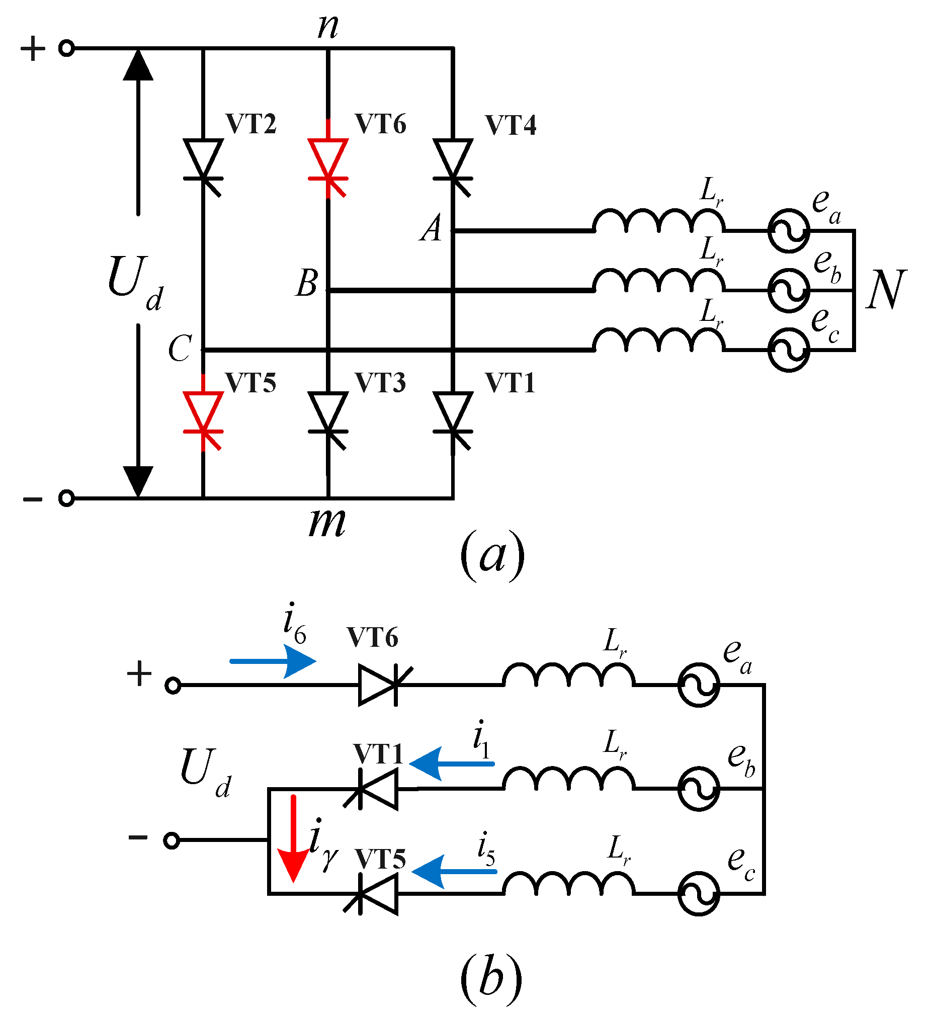
Conventional HVDC systems typically utilize three-phase bridge converters as converter units, with the fundamental structure thereof depicted in
Figure 1a. The converter valves are activated in succession from VT1 to VT6. As illustrated in the figure, the three bridge arms, labeled
A,
B, and
C, are, respectively, linked to the three phases of the inverter-side power supply. Point
n is connected to the positive terminal of the DC-side power supply, while point
m is connected to the anode. The voltage between points
n and
m constitutes DC voltage, supplying a steady unidirectional current, whereas the AC system generates the thyristor’s commutation voltage.
The influence of AC inductance in the circuit prevents the phase current from instantaneously mutating during the commutation process. The conversion of current phases requires a certain duration, referred to as commutation time or overlapping arc time. The corresponding electrical angle is known as the commutation angle or overlapping arc angle, abbreviated as μ. The electrical angle spanning from the moment the commutated valve’s current crosses 0 to the instant its applied voltage transitions from negative to positive is termed the turn-off angle or arc extinction angle, denoted as γ. If this turn-off angle is smaller than the critical one, commutation failure becomes likely. Hence, when selecting the early firing angle, it is prudent to leave some margin to prevent commutation failure.
Figure 1 illustrates the process of activating VT1 while VT5 and VT6 are already on, leading to the current in VT5 shifting to VT1. Since both terminals of VT1 are exposed to forward voltage, VT1 promptly activates and commutates upon receiving the trigger pulse. During this period, VT1, VT5, and VT6 are all conducting. However, due to the inductance in the circuit, the current transitions smoothly rather than abruptly. The currents flowing through VT1, VT5, and VT6 are denoted as
i1,
i5, and
i6, respectively. Additionally,
iγ represents the commutation currents circulating within the VT1 and VT5 circuits, sharing the same direction as
i1.
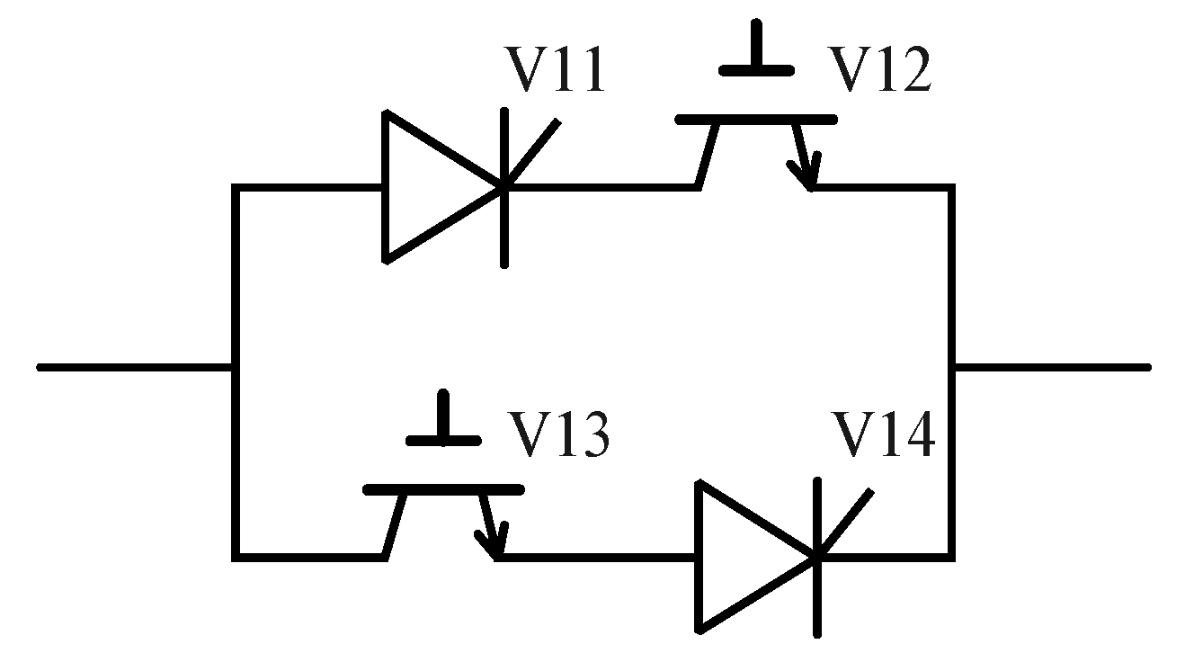
To prevent commutation failure, a thyristor, upon ceasing conduction, must be given a recovery period of at least 400 microseconds. This ensures the reliable restoration of its forward blocking capability. Following this rationale, controllable line-commutated converter (CLCC) topology becomes relevant by integrating an IGBT in series with the existing thyristor branch and introducing an auxiliary branch to facilitate commutation, as depicted in
Figure 2. In this setup, V11 and V14 are thyristors, while V12 and V13 are IGBTs. V11 and V12, connected in series, form the primary branch for high-current transmission. Conversely, V13 and V14, also in series, constitute the auxiliary branch for current transfer. During operation, the primary branch initially carries the current, with V11, V12, and V13 simultaneously activated. After 120°, the bridge arm initiates commutation. At this juncture, V12 is deactivated, while V13 and V14 of the auxiliary branch are simultaneously activated, forcing the current to commutate to the auxiliary branch. This process persists until V11 restores its forward blocking capability. Subsequently, the auxiliary branch is deactivated, awaiting the subsequent commutation cycle. This topology allows independent control of the primary and auxiliary branches, ensuring adequate recovery time for the main-branch thyristor.
2.2. The Operation Mechanism of a CLCC
The triggering logic of the novel CLCC is depicted in the accompanying
Figure 3, wherein
Sg11,
Sg12,
Sg13, and
Sg14 represent the trigger signals for the main-branch thyristor valve (V11), the main-branch full-control valve (V12), the auxiliary-branch full-control valve (V13), and the auxiliary-branch thyristor (V14), respectively. V11 is periodically triggered based on the preset firing angle. Initially, V12, V13, and V11 are simultaneously activated. Following a 120° electrical angle, V12 is concurrently deactivated with the activation of V14. This action redirects the main-branch current to the auxiliary branch, initiating the recovery process for V11. Once V11 fully restores its blocking capability, the current in V14 reaches zero, causing it to deactivate, thus completing the commutation cycle.
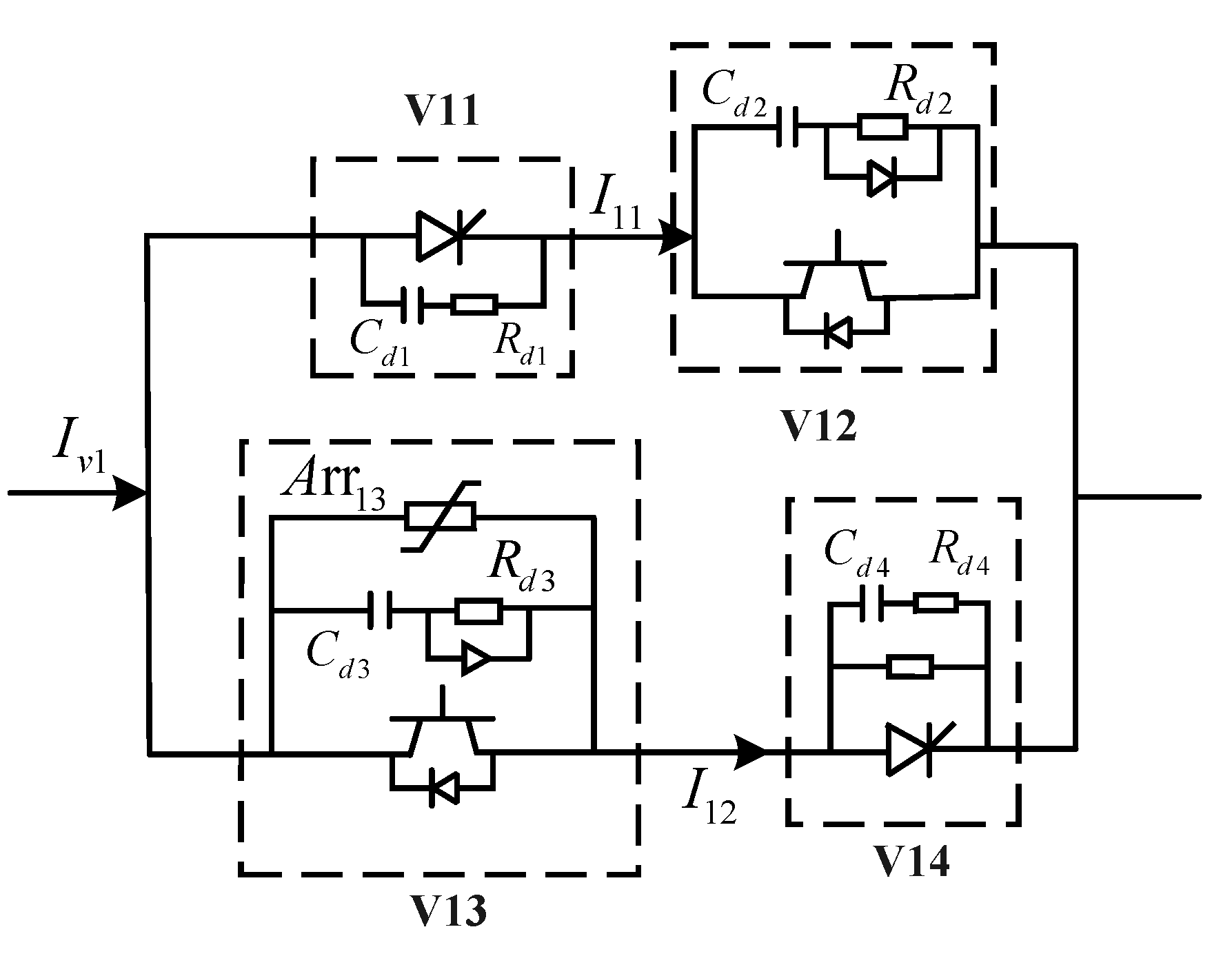
Using the VT1 converter valve as an illustrative example,
Figure 4 presents its unique internal topology. The main branch integrates the thyristor valve from a traditional LCC, with an IGBT valve connected in series, ensuring the valve group’s resilience to high voltage and currents. The primary role of the IGBT is to actively shut down and redirect the main-branch current to the auxiliary branch. Successful current transfer is ensured as long as the shutdown voltage exceeds the turn-on voltage of V13. Additionally, a metal oxide arrester (Arr13) is connected in parallel to V13, providing the necessary commutation voltage during AC-side faults and limiting potential overvoltage shutdowns.
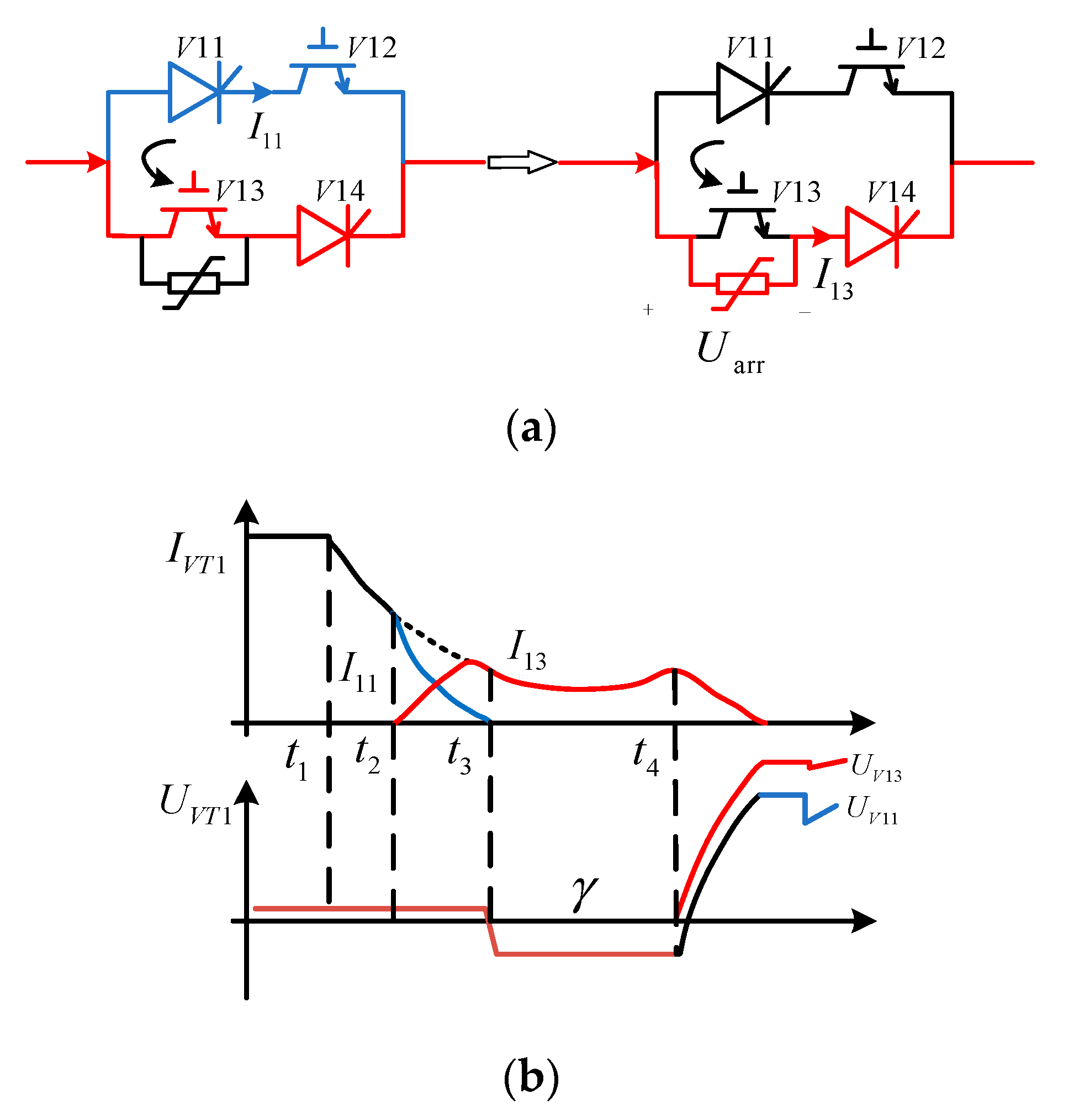
When a fault arises in the AC system at the receiving end, it leads to a drop or abnormality in the inverter-side bus voltage, subsequently causing a decrease in the DC voltage on the inverter side. Initially, the DC will increase, but it will then decrease due to the constant current control. If the fault is minor and the voltage drop is not significant, the commutation process can still proceed smoothly. However, in the event of a severe ground fault, the AC-side voltage will experience a significant drop, unable to supply the necessary commutation voltage for the inverter bridge arm, resulting in commutation failure. In such cases, the CLCC will transition to a forced-commutation state, as illustrated in
Figure 5. Specifically, (a) represents the circuit model during forced commutation, while (b) depicts the associated current and voltage variations in this state.
Prior to activating the auxiliary branch, the main branch operates similarly to its normal state. At this point, V12 is shut off. Consequently, the current shifts to the auxiliary branch, while the main-branch current, which cannot abruptly change, charges the capacitor paralleled with V12. Once the main-branch current reaches zero, V11 is deactivated, and a reverse voltage is applied to it, ensuring that V11 is securely turned off.
Given that the current during a fault condition is elevated, it requires a longer duration to taper down to zero. However, as long as the auxiliary branch remains conductive, the reverse voltage on V11 will persist. After V11 fully regains its blocking capability, V13 interrupts the high current and redirects it to the metal oxide arrester (Arr13) paralleled with it. This triggers the arrester, establishing a protective voltage. When combined with the commutation voltage, this compels the bridge arm current to commutate to the succeeding valve group.
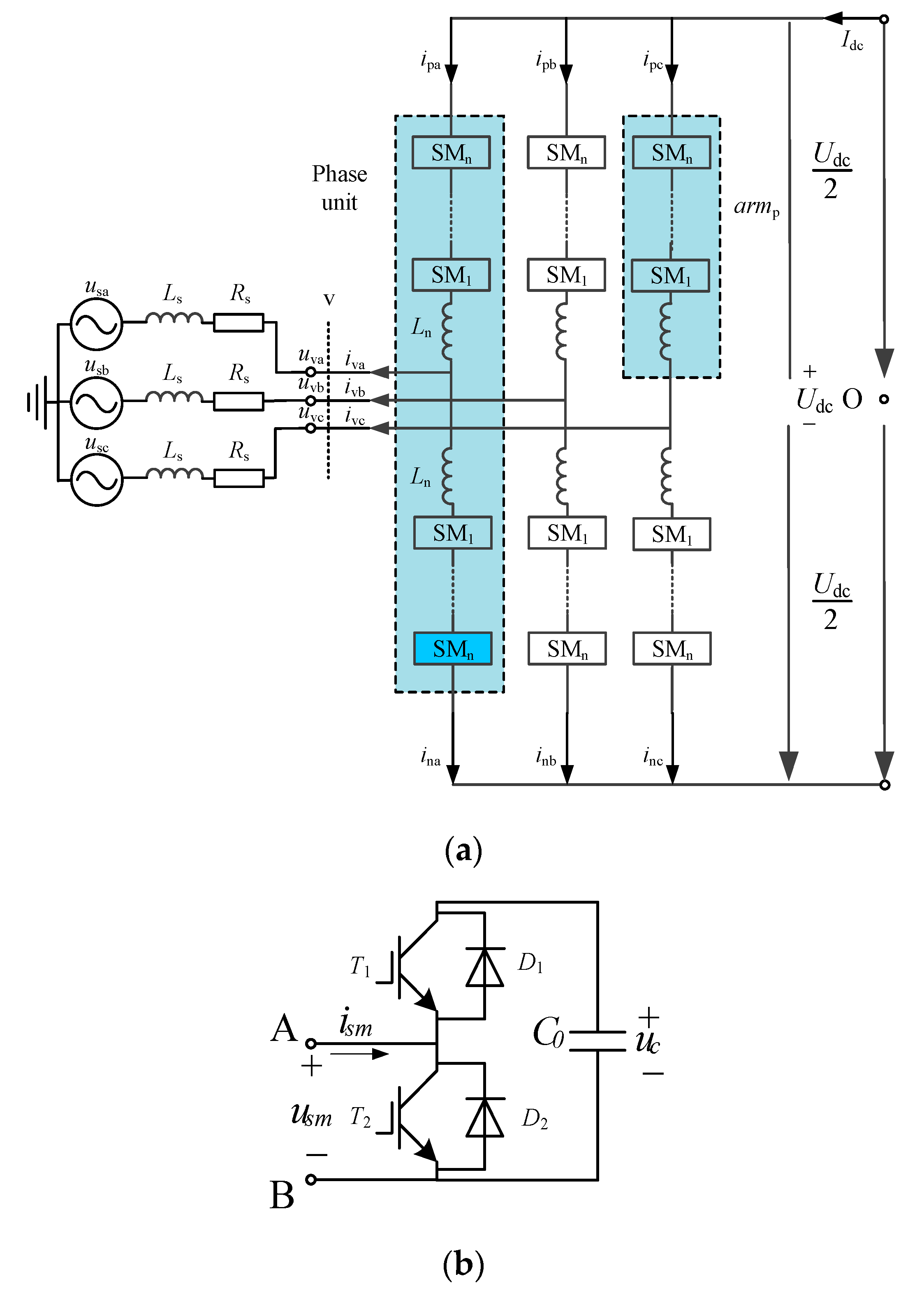
2.3. The Basic Structure of a VSC-HVDC
The topology of a VSC-HVDC converter station, specifically focusing on the basic structure of the half-bridge MMC, is presented in
Figure 5. The converter station receives three-phase ACs, which are injected into the corresponding bridge arm nodes. Multiple submodules, each composed of thyristors
T1 and
T2, diodes
D1 and
D2, and an energy storage capacitor
C0, are cascaded and connected in series to form the bridge-arm inductor
Ln, which comprises both the upper and lower bridge arms, as
Figure 6 shows. Notably, all phase units share identical parameters and structures, and the submodules within each unit are also uniformly designed. By adjusting the number of submodules being inserted or removed, the output voltage level and power can be precisely and flexibly controlled.
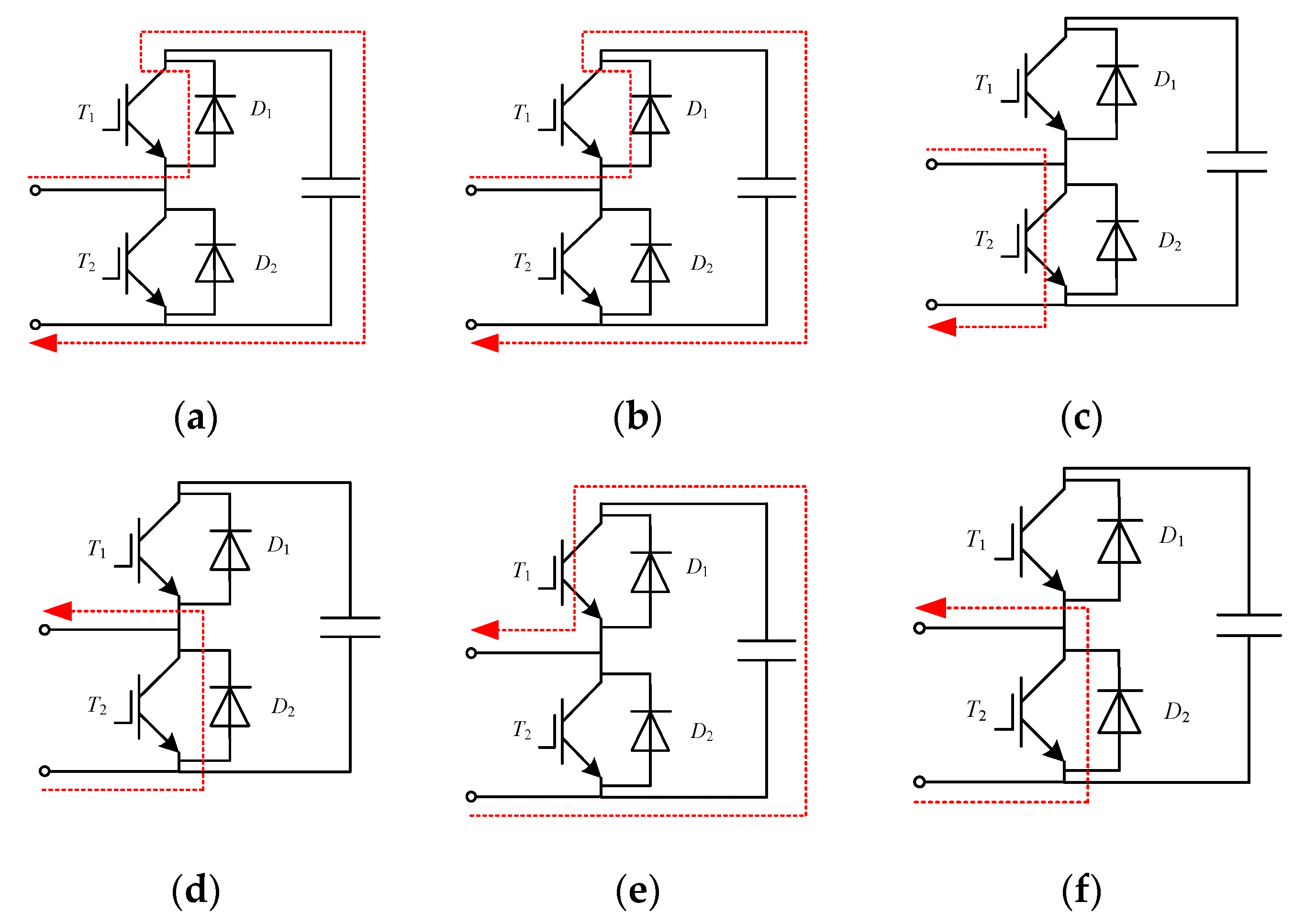
The submodule exhibits three distinct working states, as follows: both
T1 and
T2 are blocked;
T1 is activated, while
T2 is blocked; and
T1 is blocked, while
T2 is activated. These three operating states are clearly illustrated in
Figure 7.
When T1 and T2 are both deactivated, the forward operating current passes through the freewheeling D1, charging the capacitor. This specific operating mode is exclusive to the initial startup phase of the converter station. During this phase, the AC system charges the capacitor until its voltage reaches the rated level. Conversely, when both T1 and T2 are deactivated and the negative operating current bypasses the capacitor via the freewheeling D2, the entire submodule is bypassed and rendered inactive. This mode is triggered only in case of a converter station malfunction or when a submodule is removed.
In the case where T1 is activated and T2 is deactivated, the forward operating current charges the capacitor through D1, while the negative operating current discharges the capacitor through T1. Under these conditions, the current can bidirectionally flow. Notably, regardless of the current’s direction, the submodule’s output voltage corresponds to the voltage across the capacitor, indicating that the submodule is actively operational.
When T1 is deactivated and T2 is activated, the operating current bypasses the capacitor through T1 or D2, effectively bypassing the entire submodule. In this mode, the capacitor remains undischarged due to the absence of a discharge path, maintaining a constant voltage at both ends. Consequently, the output terminal voltage remains at zero. This operating mode is solely employed when designing redundant submodules.
Based on the above submodule characteristics, the nearest-level modulation technology is used by changing the number of input submodules on the upper and lower bridge arms and continuously approaching the modulation wave to achieve the rectification and inverter functions.


