Article

A New Approach to Examine the Dynamics of Switched-Mode Step-Up DC–DC Converters—A Switched State-Space Model

Department of Automatic Control and Robotics, Faculty of Electrical Engineering, Bialystok University of Technology, Wiejska 45D Street, 15-351 Bialystok, Poland
*
Author to whom correspondence should be addressed.
Energies 2024, 17(17), 4413; https://doi.org/10.3390/en17174413
Submission received: 24 June 2024 / Revised: 20 August 2024 / Accepted: 30 August 2024 / Published: 3 September 2024
(This article belongs to the Section F3: Power Electronics)

Abstract

:
Power electronic converters are important elements of many modern devices. Therefore, there is a need for a thorough analysis of their behavior and the ability to properly control them. Typically, the converter’s dynamics are investigated using the small-signal averaging method, which does not provide detailed information about the converter. In particular, it does not account for the switching ripple effect. In this paper, a novel switched state–space model of the interleaved step-up DC–DC converter is introduced. That model incorporates high-frequency information, which allows for a more in-depth dynamics analysis. The results, i.e., step and frequency responses, obtained from both theoretical models are compared to the interleaved step-up DC–DC converter model implemented in PSpice ver. 16.6 from Cadence Design Systems.

1. Introduction

The widespread use of step-up DC–DC converters in modern appliances [1] necessitates an accurate dynamic model for investigating stability and designing effective controllers. With increasing demand for power converters, a subject of high efficiency at high-rated power becomes more meaningful [2,3]. Many step-up topologies of DC–DC converters can be connected in parallel to increase the overall power rating of the converter, maintaining a single phase to work at a high-efficiency region. Multi-phase, interleaved DC–DC converters are composed of several identical phases driven interchangeably [4,5,6]. This type of topology can be effectively applied in renewable energy systems, where low voltage delivered by renewable energy generators or batteries in the range of tens of volts need to be stepped up to the level of hundreds of volts at the converter’s output [7].
Switched-mode DC–DC converters are nonlinear, time-discontinuous electronic circuits. Typically, the dynamics of DC–DC converters are investigated using small-signal averaging [8], which involves linearizing the time-discontinuous system in the steady state across periodic operating points or determining a linear trajectory with small-signal perturbations [9], resulting in linear time-invariant or linear time-periodic small-signal models, respectively. This approach transforms the time-discontinuous system into a time-continuous system, enabling further linear analysis [10].
While small-signal averaging provides a good understanding of DC–DC converter dynamics and is usually sufficient to design the controller, it does not account for the switching ripple effect. These phenomena cannot be neglected in resonant converters [11,12] or high-ripple DC–DC converters such as multi-phase interleaved topologies. In microgrid installations [13], the interaction of multiple DC–DC converters operating at different switching frequencies on a common DC bus rail introduces beat frequency oscillations causing system instability [14,15]. For this reason, it is essential to investigate the high-frequency dynamics of DC–DC converters to assess beat frequency oscillations and to design a robust control loop that suppresses beat frequency disturbances [15]. For the reasons mentioned above, the small-signal averaging method is insufficient, as it is only suitable for estimating the dynamic performance of the converter up to half the switching frequency, excluding high-frequency sideband subharmonics introduced by the PWM driving method.
Various methods have been developed to address the limitations of small-signal averaging [16], such as the multi-frequency small-signal model [17] and the modified averaged model, which introduce a sample-and-hold effect to account for high-frequency components of constant-frequency PWM modulation [18]. The describing function method [19] and generalized state–space average model [20] are more advanced techniques that can be applied to both constant and variable frequency modulation methods.
Many practical systems can be modeled by a set of subsystems and a logical rule that describes switching between them. Therefore, such systems are efficiently represented by switched dynamical systems, which have attracted much attention from researchers in the last two decades [21]. Due to such operation of power electronic converters, the switched systems theory is suitable for describing their dynamical properties. A DC–DC converter as a whole, consists of a power stage, which is an open-loop dynamical system, and a control unit. The power stage itself is a strictly non-linear object, and it works in several discontinued states. Power conversion is achieved by switching between several linear circuits that comprise the energy storage components: inductor and capacitor. The switching function is performed by transistors and diodes. In the literature, attempts have been made to use the theory of switched systems in relation to DC–DC converters, but these considerations focused mainly on the application of that approach to the control and stabilization of the converters [22,23,24,25,26,27]. To the best of the authors’ knowledge, no one has yet attempted to analyze and model the high-frequency phenomena of DC-DC converters associated with the PWM driving method using the switched state–space method.
This paper presents a new approach to modeling the dynamics of DC–DC converters, incorporating high-frequency information based on a new form of switched state–space modeling [21] of the DC–DC converter dynamics. The method will be demonstrated on the example of a multi-phase interleaved tapped-inductor step-up DC-DC converter. In contrast to single-phase topologies, in multi-phase interleaved DC–DC converters, the high-frequency product of switching is more noticeable. Each phase of the multi-phase converter is driven by the same switching frequency with a phase shift, introducing multiple sideband products of the switching frequency. The paper will present the small-signal model of the converter, predicting dynamics below half the switching frequency region. Subsequently, the switched state–space model, as an extension of the small-signal averaging model, will include information about multi-phase switching ripples. Finally, the results of switched state–space modeling will be confirmed by comparing them with the small-signal averaging model and the PSpice model of the multi-phase tapped-inductor step-up DC–DC converter in both time and frequency domains.

2. Interleaved Step-Up DC–DC Converter

The major advantage of this topology is its simplicity (i.e., small number of components per phase), allowing high efficiency and high power density of the whole interleaved system. The converter is composed of n identical sections (phases) connected in parallel and driven interchangeably.

2.1. Topology of the Converter

The topology of the tapped-inductor step-up DC–DC converter is depicted in Figure 1. The energy is stored in a magnetic field of the coupled inductors L 1 and L 2 while transistor T is turned on. In contrast to the flyback topology, the coupled inductors are connected in series, i.e., in the tapped configuration [28]. At transistor turn-off, the energy is transferred through diode D to the load R o , and the clamping diode D p suppresses the voltage spikes on the transistor to not exceed the level of the output voltage V o and transfers the leakage energy directly to the output.
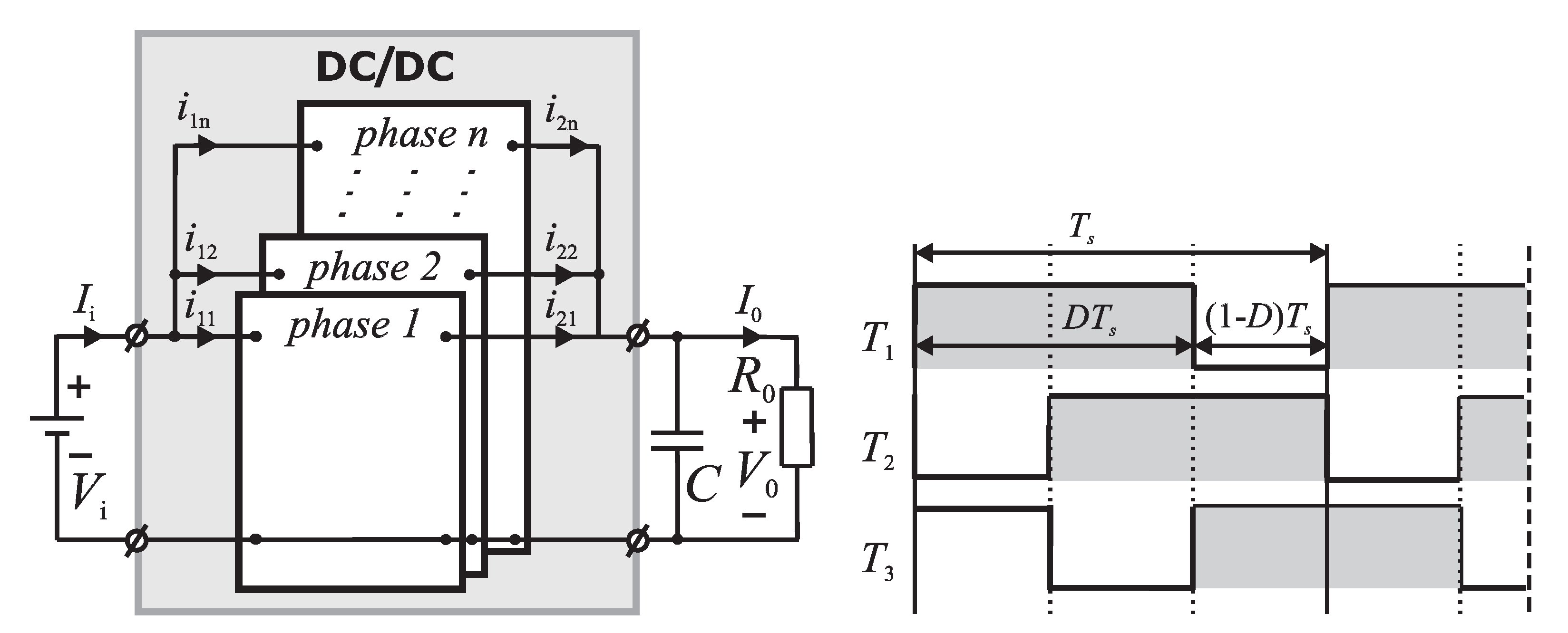
The multi-phase topology and interleaved driving of the sections are presented in Figure 2.
Parasitic parameters of the electronic components need to be considered in the model to confirm the dynamic performance of the converter’s model with PSpice simulation results (Figure 3). Therefore, a more detailed analysis of the converter’s work needs to be carried out. Thus, the leakage inductance L l k , which is caused by the non-ideal coupling between the primary and secondary windings of the inductor, is represented by a coupling coefficient k < 1 . The required output voltage is achieved by the utilization of coupled inductors with a turns ratio of N = L 2 / L 1 and an adjusting duty cycle D of the transistors’ driving signals (right-side picture of Figure 2). The model also includes parasitic resistances of individual circuit elements (see details in Section 2.4).
Moreover, the instantaneous transients during transistor turn-off are neglected, since they do not affect the dynamic behavior of the converter. Therefore, the branch with diode D p can be omitted (Figure 3).

2.2. Time Domain Analysis of the Converter’s Work

The operation of the interleaved converter composed of n sections depicted in Figure 3 can be expressed by
d i 1 d t = r 1 + r T L 1 ( 2 k ) i 1 + 1 L 1 ( 2 k ) V i d u C d t = n C ( R o + r C ) u C ( 0 < t < D T s ) ,
d i 1 d t = r 1 + r 2 + r D L 1 ( N + 1 ) 2 i 1 R o L 1 ( N + 1 ) ( R o + r C ) u C + 1 L 1 ( N + 1 ) V i d u C d t = n R o C ( N + 1 ) ( R o + r C ) i 1 1 C ( R o + r C ) u C ( D T s < t < T s ) ,
where inductor current i 1 and output capacitor voltage u C will be considered as state–space variables. Equation (1) describes the operation of the converter (Figure 3) at transistor turn-on, whereas Equation (2) expresses the state of the converter at the transistor turn-off period (Figure 2).

2.3. Active Component Choice

Considering the input voltage of V i = 40 V DC, due to boosting the voltage up to around 500 V DC, a ten-fold voltage gain is required. Considering (1) and (2) in the steady state and applying the volt-second balance across the switching period and neglecting parasitics, the following voltage gain formula can be obtained:
V o V i = 1 + N D 1 D .
Thus, for a turns ratio of around N = 4 , the required duty cycle would not exceed 0.7 . Assuming ideal coupling between the inductor’s primary and secondary windings ( k = 1 ), the voltage stress V T on the transistor can be expressed as
V T = N V i + V o 1 + N .
Likewise, the voltage stress V D on the output diode D is
V D = V o N V i .
Based on (4), a 650 V MDmesh STW88N65M5 power switch from ST Microelectronics was chosen and, considering (5), a silicon carbide fast switching 1200 V CSD10120 diode from Cree Power was selected to carry out the PSpice simulations.

2.4. Assumptions to the Model

Parasitic resistances have an impact on the dynamical behavior of the converter introducing a damping effect. In order to compare the results of theoretical modeling with the PSpice simulation outcome, the parasitic parameters of the real components need to be considered. Thus, the non-ideal magnetic coupling of coupled inductor’s windings (i.e., k < 1 ), as well as parasitic resistances, were taken into account (Figure 3) and collated in Table 1.
The model of the converter was derived with the following assumptions:
  • The transistor during the on period is represented by constant drain-to-source resistance r T ;
  • The conducting diode is represented by its series dynamic resistance r D ;
  • Diodes and transistors during the turn-off period are considered infinite resistances;
  • The resistances of the inductor windings (i.e., r 1 and r 2 ) include both DC and AC resistance components [29];
  • The inductor operates in the linear part of its B H curve;
  • The converter operates in constant current mode (CCM);
  • The rated power of a single phase does not exceed 650 W.

3. Converter Dynamics Analysis

In this section, we present the converter’s state–space model obtained from its time domain analysis. Then, the small-signal averaged model based on the averaging of state variables across the single switching period will be demonstrated. Finally, this model will be extended to the switched state–space model by splitting the total n-phase converter input current i 1 into separate currents (i.e., separate state variables) for each converter’s phase and introducing interleaved PWM driving of the phases.

3.1. Small-Signal Averaging Method

The Equations (1) and (2) can be written in the form of a state–space model given by
x ˙ ( t ) = A k x ( t ) + B k u ( t ) , k = { 1 , 2 } , y ( t ) = C x ( t ) ,
where x ( t ) R 2 is the state vector, u ( t ) R is the input, and y ( t ) R 2 is the output vector expressed by
x ( t ) = y ( t ) = i 1 ( t ) u C ( t ) , u ( t ) = V i
and the matrices A k R 2 × 2 , B k R 2 × 1 for k = { 1 , 2 } are defined as
A 1 = r 1 + r T L 1 ( 2 k ) 0 0 n C ( R o + r C ) , B 1 = 1 L 1 ( 2 k ) 0 , A 2 = r 1 + r 2 + r D L 1 ( N + 1 ) 2 R o L 1 ( N + 1 ) ( R o + r C ) n R o C ( N + 1 ) ( R 0 + r C ) 1 C ( R 0 + r C ) , B 2 = 1 L 1 ( N + 1 ) 0 .
The matrices A 1 , B 1 describe the converter dynamics in D T s period, and the matrices A 2 , B 2 represent the ( 1 D ) T s period (Figure 2). In further considerations, we assume a capacitor voltage of u C ( t ) as the system output. Therefore, the matrix C R 1 × 2 has the form
C = 0 1 .
Averaging the state variables across the single switching period T s , the state–space model (6) can be rewritten as
x ˘ ˙ ( t ) = A x ˘ ( t ) + B u ˘ ( t ) , y ˘ ( t ) = C x ˘ ( t ) ,
where x ˘ ( t ) R 2 , u ˘ ( t ) R , and y ˘ ( t ) R 2 are the average values of the state vector, input, and output vector (respectively), and the matrices A R 2 × 2 , B R 2 × 1 are given by
A = A 1 D + ( 1 D ) A 2 = ( 1 D ) ( r 1 + r 2 + r D ) L 1 ( N + 1 ) 2 D ( r 1 + r T ) L 1 ( 2 k ) R o ( 1 D ) L 1 ( N + 1 ) ( R o + r C ) n R o ( 1 D ) C ( N + 1 ) ( R o + r C ) 1 + D ( n 1 ) C ( R o + r C ) , B = B 1 D + ( 1 D ) B 2 = 1 D L 1 ( N + 1 ) + D L 1 ( 2 k ) 0 .
The matrix C in (10) is given by (9).
The advantage of the model (9) and (11) is its simplicity. However, it includes only the averaged values of the state variables, excluding above half the switching frequency information. Moreover, the above model assumes that all phases are active/inactive in the converter at the same time, which does not occur in the real system.

3.2. Switched State–Space Model Approach

To overcome the disadvantages of the averaging method, we introduce the switched state–space model in the universal n-phase form:
x ¯ ˙ ( t ) = A s w x ¯ ( t ) + B s w u ( t ) , y ¯ ( t ) = C s w x ¯ ( t ) ,
where
x ¯ ( t ) = y ¯ ( t ) = i 11 ( t ) i 12 ( t ) i 1 n ( t ) u C ( t ) R n + 1 , u ( t ) = U i n R
and the matrices A s w R ( n + 1 ) × ( n + 1 ) , B s w R ( n + 1 ) × 1 , and C s w R 1 × ( n + 1 ) are defined by
A s w = a 1 S 1 + a 2 ( 1 S 1 ) 0 0 0 a 3 ( 1 S 1 ) 0 a 1 S 2 + a 2 ( 1 S 2 ) 0 0 a 3 ( 1 S 2 ) 0 0 0 a 1 S n + a 2 ( 1 S n ) a 3 ( 1 S n ) a 4 ( 1 S 1 ) a 4 ( 1 S 2 ) a 4 ( 1 S 3 ) a 4 ( 1 S n ) a 5 ( S 1 + S 2 + + S n ) , B s w = 1 L 1 ( 2 k ) S 1 + 1 L 1 ( N + 1 ) ( 1 S 1 ) 1 L 1 ( 2 k ) S 2 + 1 L 1 ( N + 1 ) ( 1 S 2 ) 1 L 1 ( 2 k ) S n + 1 L 1 ( N + 1 ) ( 1 S n ) 0 , C s w = 0 0 0 0 1
with
a 1 = r 1 + r T L 1 ( 2 k ) , a 2 = r 1 + r 2 + r D L 1 ( N + 1 ) 2 , a 3 = R o L 1 ( N + 1 ) ( R o + r C ) , a 4 = R o C ( N + 1 ) ( R 0 + r C ) , a 5 = 1 C ( R o + r C )
and
S k = { 0 , 1 } f o r k = { 1 , 2 , , n } .
The variables S k , k = { 1 , 2 , , n } are related to the PWM signals controlling the transistors in the correspondent phases. They change their value from 0 to 1 (or vice versa) according to the switching frequency. Instead of one state variable i 1 ( t ) being responsible for the total converter current presented in the model (6), we introduce currents i 1 k ( t ) , k = { 1 , 2 , , n } associated with specific phases of the converter in order to reflect interleaved PWM driving.
In the literature, the switched state–space model often consists of a set of matrices and a switching function with values corresponding to the appropriate subsystems. This versatile description of the switched system (12)–(16) allows us to take into account all possible configurations of the system without unnecessarily defining a set of models for each switching, which originally would grow exponentially with the number of converter phases. Additionally, with this approach, there is no need to define a complicated multi-value switching function.
The considered switched state–space model allows for a more in-depth dynamics analysis than the model obtained by the averaging method, because it takes into account the dynamics of each phase independently and introduces sideband subharmonics caused by the interleaved PWM driving method.

3.3. PSpice Model

To confirm the theoretical approach, a PSpice model of the interleaved tapped-inductor step-up DC–DC converter was developed (Figure 4). The model includes parasitic series resistances of the windings and the output capacitor (ESR). The parasitic resistances of the transistor and diodes are incorporated in relevant PSpice models. Additionally, the transistors’ driving circuits composed of R g and C g improve transistor turn-off.

4. Results

In this section, we present the analysis of the converter dynamics based on the step responses with 1 V input signal change, as well as frequency responses in the range of 15 Hz–220 kHz. The load resistances and duty cycles for the selected number of phases were determined to secure the converter’s operation in both the half-rated power and full power of a single phase. Thus, four combinations of the number of converter phases and duty cycles were considered:
1.
n = 3 , D = 0.6 , and R o = 127   Ω (half-rated power);
2.
n = 3 , D = 0.7 , and R o = 127   Ω (full power);
3.
n = 5 , D = 0.6 , and R o = 77   Ω (half-rated power);
4.
n = 5 , D = 0.7 , and R o = 77   Ω (full power).
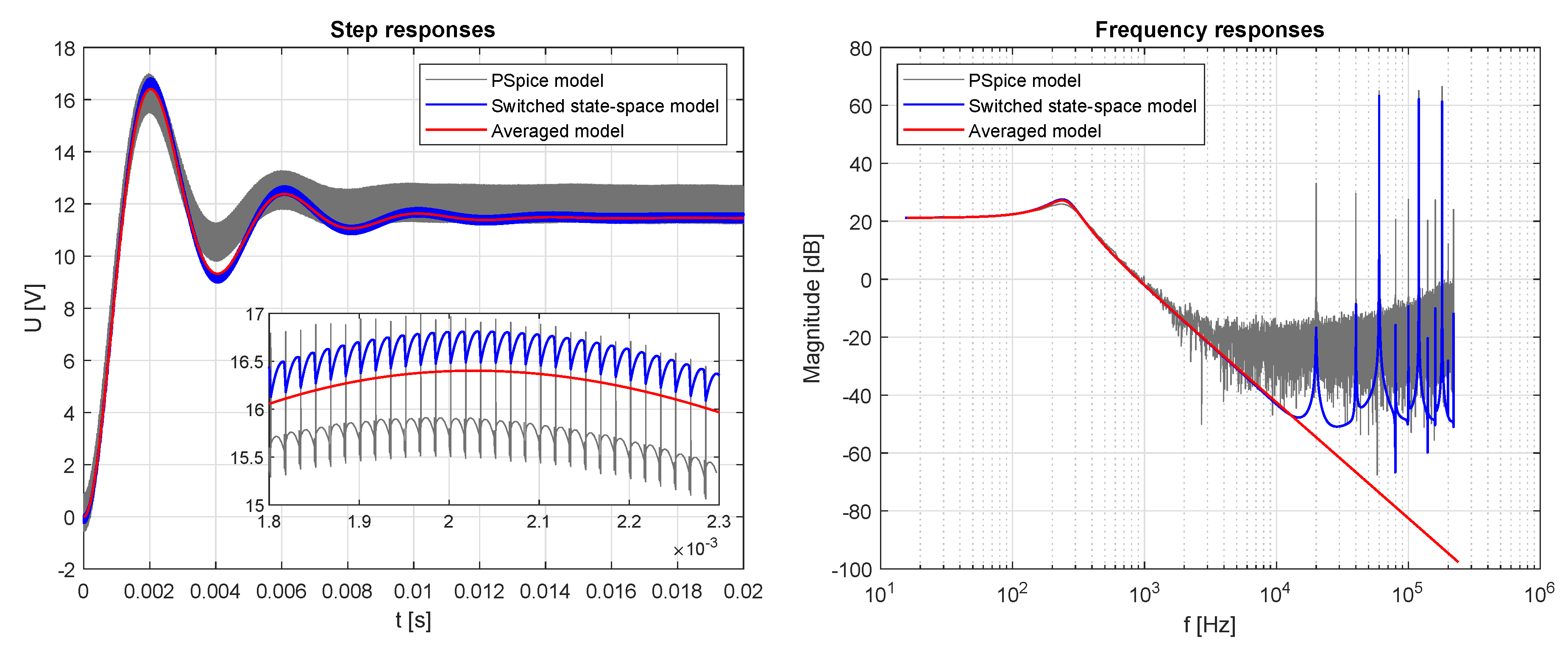
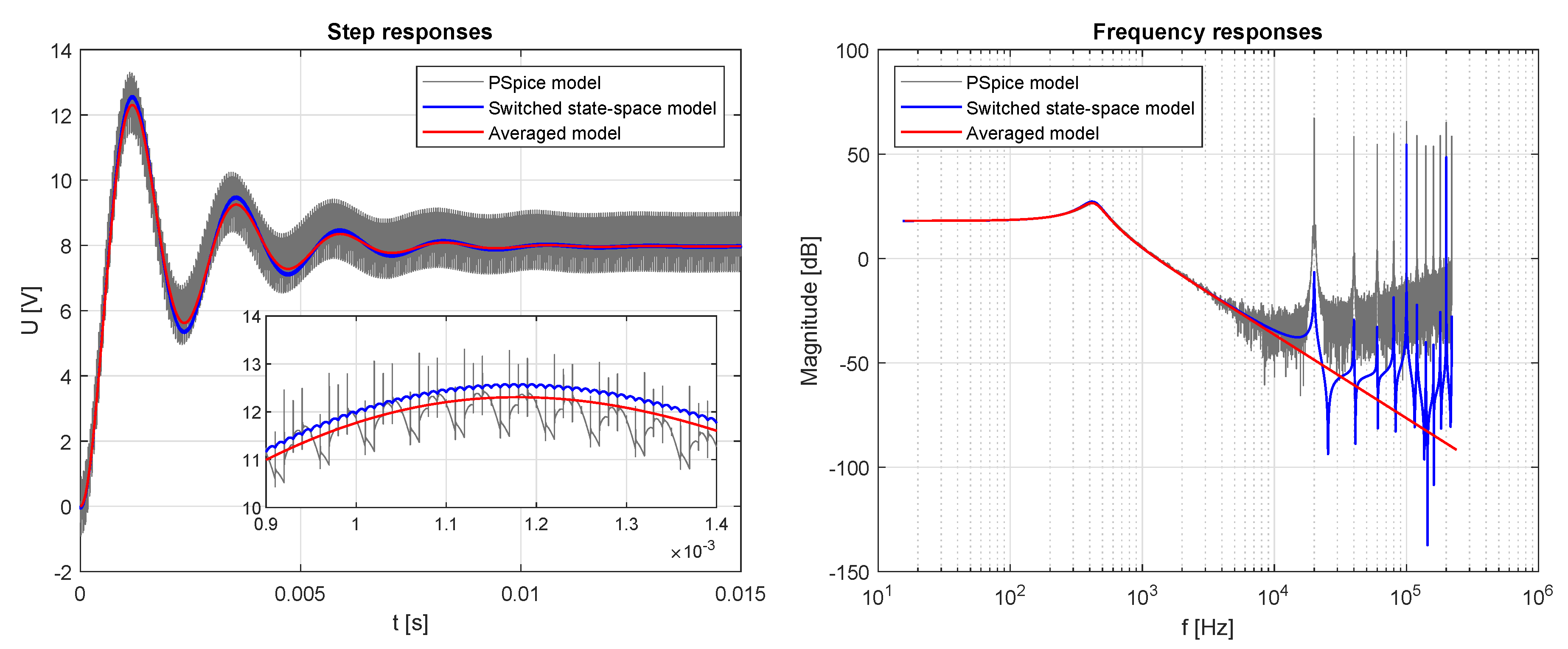
The results obtained for the PSpice model, the averaged model (9)–(11), and the switched state–space model (12)–(16) are presented in the Figure 5, Figure 6, Figure 7 and Figure 8. The following figures of step responses additionally show an enlarged fragment around the amplitude of the first peak of oscillation.
In Figure 5, Figure 6, Figure 7 and Figure 8, the averaged model was found to show no high-frequency ripples simultaneously reflecting the PSpice model’s step response. The switched state–space model showed a high-frequency product of the PWM driving, which is similar to the frequency response of the PSpice model in the range above half the switching frequency. In further analyses, both the small-signal averaging models (9)–(11) and the switched state–space models (12)–(16) will be compared to the PSpice simulation.

5. Discussion

To quantitatively evaluate the results, the following parameters were introduced (Figure 9):
  • Δ V A 1 , Δ V A 2 , and Δ V S S —relative errors of the first and second oscillations’ peak amplitudes and the relative error of the steady state value expressed by
    Δ V A j = V A j , P S p i c e V A j V A j , P S p i c e · 100 % , j = { 1 , 2 } , Δ V S S = V S S , P S p i c e V S S V S S , P S p i c e · 100 % ,
    where values for the PSpice and switched state–space models were computed as average values over one period;
  • Δ t m a x —maximum time shift between oscillations peak amplitudes over the entire response;
  • Δ t r i s e —difference between rise times, i.e., times taken by signals to change from 0.1 V S S to 0.9 V S S .
The above-mentioned parameters are listed in Table 2.
In all the considered cases, the Δ t m a x parameter did not exceed 0.1 ms. Moreover, the Δ t r i s e parameter was within 11 μ s for the switched model and 25 μ s for the averaged model, where in each case, the switched model achieved values approximately twice lower. Therefore, we obtained a high consistency for all the models in terms of the durations of transient processes, with a noticeable advantage regarding the switched state–space method. All of the presented approaches also featured a small steady state voltage error ( 0.63 % in the worst case), which translates into good static parameters regarding the considered models.
However, some differences can be noticed in the initial part of the trajectory. In the case of a 5-phase converter, the errors of Δ V A 1 and Δ V A 2 were relatively small, taking values below 3 % in most situations. These errors were significantly higher for a 3-phase converter, especially with duty cycle D = 0.6 . However, it should be noted that the signal shape is well reproduced, except for the excessive magnitude of the frequency peak within the range of 200–400 Hz, which can be seen in the frequency responses in Figure 5 and Figure 6.
The greatest differences in the averaged and switched models can be observed in the frequency responses. In the range of 15 Hz to 2–3 kHz, they were almost identical to the PSpice model responses, with a certain difference in the magnitude in the above-mentioned range of 200–400 Hz in a 3-phase converter. The difference was 2.25 dB for D = 0.6 and 1.22 dB for D = 0.7 . Above these frequencies, the frequency responses for all models retained a roll-off gain of 40 dB/decade up to 220 kHz. On the other hand, the switched model response features magnitude peaks at multiples of the PWM frequency (multiples of 20 kHz), with particular magnitude notches for multiples of 60 kHz (for the 3-phase converter) and 100 kHz (for the 5-phase converter). These peaks correspond to the peaks obtained in the PSpice model, which indicates that the switched model incorporates accurate high-frequency information that was completely missed by the averaged model.

6. Conclusions

In this paper, a new approach to modeling the dynamics of switched-mode DC–DC converters has been proposed. In particular, a method incorporating high-frequency information based on switched state–space modeling has been introduced. The main contributions of this paper can be summarized as follows:
  • An interleaved tapped-inductor step-up DC–DC converter model with parasitic parameters of the components has been developed. Based on this proposition, the small-signal averaged model of the converter has been obtained.
  • A novel switched state-space model of the analyzed converter has been derived from state–space equations and compared to the small-signal averaged model, showing the advantages of the former one.
  • The effectiveness of the presented approach has been demonstrated and discussed in comparison with the PSpice simulation results.
It has been shown that in the time domain, both averaged and switched models give similar results, reproducing the output voltage shape accurately. The biggest advantage of the switched state–space model is the high-frequency information outlining the effect of the PWM driving method on the voltage waveform and the sideband harmonics contained therein. The results are consistent with the outcomes of PSpice model simulations. The proposed approach of the switched space–state method can be successfully applied to other switched-mode converters that are described by state–space equations or small-signal averaged model, introducing a description of high-frequency component into the modeling. Furthermore, switched state–space modeling can be helpful in the analysis and synthesis of control algorithms in microgrid installations, where the high-frequency dynamics examination of DC–DC converters is important to estimate beat frequency oscillations that may cause system instability.

Author Contributions

The authors A.T. and K.B. have written and edited the paper. All authors have read and agreed to the published version of the manuscript.

Funding

The studies have been carried out in the framework of work No. WZ/WE-IA/5/2023 and financed from the funds for science by the Polish Ministry of Science and Higher Education.

Data Availability Statement

The original contributions presented in the study are included in the article, further inquiries can be directed to the corresponding author.

Conflicts of Interest

The authors have no conflicts of interest to declare.

References

  1. Blaabjerg, F.; Guerrero, J.M. Smart grid and renewable energy systems. In Proceedings of the 2011 International Conference on Electrical Machines and Systems, Beijing, China, 20–23 August 2011; pp. 1–10. [Google Scholar]
  2. Blaabjerg, F.; Yang, Y.; Ma, K.; Wang., X. Power electronics—The key technology for renewable energy system integration. In Proceedings of the 2015 International Conference on Renewable Energy Research and Applications (ICRERA), Palermo, Italy, 22–25 November 2015; pp. 1618–1626. [Google Scholar]
  3. Blaabjerg, F.; Iov, F.; Kerekes, T.; Teodorescu, R. Trends in power electronics and control of renewable energy systems. In Proceedings of the 14th International Power Electronics and Motion Control Conference EPE-PEMC 2010, Ohrid, North Macedonia, 6–8 September 2010; pp. K–1–K–19. [Google Scholar]
  4. Dwari, S.; Parsa, L. A Novel High Efficiency High Power Interleaved Coupled-Inductor Boost DC-DC Converter for Hybrid and Fuel Cell Electric Vehicle. In Proceedings of the 2007 IEEE Vehicle Power and Propulsion Conference, Arlington, TX, USA, 9–12 September 2007; pp. 399–404. [Google Scholar]
  5. Li, W.; Xiang, X.; Li, C.; Li, W.; He, X. Interleaved High Step-Up ZVT Converter With Built-In Transformer Voltage Doubler Cell for Distributed PV Generation System. IEEE Trans. Power Electron. 2012, 28, 300–313. [Google Scholar] [CrossRef]
  6. Gitau, M.N.; Hofsajer, I.W. Analysis of a 4-phase tapped-inductor DC-DC converter for high boost ratio wide input voltage range applications. In Proceedings of the IECON 2014—40th Annual Conference of the IEEE Industrial Electronics Society, Dallas, TX, USA, 29 October–1 November 2014; pp. 5468–5474. [Google Scholar]
  7. Tomaszuk, A.; Krupa, A. High efficiency high step-up DC/DC converters—A review. Bull. Pol. Acad. Sci. Tech. Sci. 2011, 59, 475. [Google Scholar] [CrossRef]
  8. Erickson, R.W.; Maksimović, D. Fundamentals of Power Electronics, 3rd ed.; Springer: Cham, Switzerland, 2020. [Google Scholar]
  9. Kazimierczuk, M.K. Pulse-Width Modulated DC-DC Power Converters, 2nd ed.; Wiley: Hoboken, NJ, USA, 2015. [Google Scholar]
  10. Antsaklis, P.J.; Michel, A.N. Linear Systems; Birkhäuser: Boston, MA, USA, 2005. [Google Scholar]
  11. Chakraborty, S.S.; Hatua, K.; Bhattacharya, S. A Control Method to Reduce Overshoots in High-Frequency Link Current and Voltages at Load Transients of a Dual-Active-Bridge Series-Resonant Converter. IEEE J. Emerg. Sel. Top. Power Electron. 2023, 4, 525–537. [Google Scholar] [CrossRef]
  12. Harasimczuk, M.; Kopacz, R.; Tomaszuk, A. Lossless Clamp Circuit With Turn-OFF Voltage and Current Reduction in High Step-Up DC–DC Converter With Coupled Inductor. IEEE Trans. Power Electron. 2024, 39, 1074–1086. [Google Scholar] [CrossRef]
  13. Zhang, J. Analysis of High Gain DC-DC Converters for DC Microgrid. In Proceedings of the 2023 IEEE 3rd International Conference on Power, Electronics and Computer Applications (ICPECA), Shenyang, China, 29–31 January 2023. [Google Scholar]
  14. Xu, H.; Zhu, Y.; Lin, Z. Beat Frequency Oscillation Analysis for a DC Microgrid with Multiple Boost Converters. In Proceedings of the 2023 IEEE 14th International Symposium on Power Electronics for Distributed Generation Systems (PEDG), Shanghai, China, 9–12 June 2023; pp. 866–870. [Google Scholar]
  15. Yue, X.; Boroyevich, D.; Lee, F.C.; Chen, F.; Burgos, R.; Zhuo, F. Beat Frequency Oscillation Analysis for Power Electronic Converters in DC Nanogrid Based on Crossed Frequency Output Impedance Matrix Model. IEEE Trans. Power Electron. 2018, 33, 3052–3064. [Google Scholar] [CrossRef]
  16. Yue, X.; Wang, X.; Blaabjerg, F. Review of Small-Signal Modeling Methods Including Frequency-Coupling Dynamics of Power Converters. IEEE Trans. Power Electron. 2018, 34, 3313–3328. [Google Scholar] [CrossRef]
  17. Xiangpeng, C.; Jinjun, L.; Danhong, X.; Zipeng, L. An Enhanced Multi-frequency Small-signal Model for the Close-loop Design in Buck Converters. In Proceedings of the 2018 IEEE Energy Conversion Congress and Exposition (ECCE), Portland, OR, USA, 23–27 September 2018; pp. 1453–1458. [Google Scholar]
  18. Xiangpeng, C.; Jinjun, L.; Yiming, T.; Danhong, X. A Comparison of Average Model, Sampled-data Model and Multi-frequency Model Based on DC/DC Converters. In Proceedings of the 2018 International Power Electronics Conference (IPEC—Niigata 2018—ECCE Asia), Niigata, Japan, 20–24 May 2018; pp. 2435–2440. [Google Scholar]
  19. Li, J.; Lee, F.C. New Modeling Approach and Equivalent Circuit Representation for Current-Mode Control. IEEE Trans. Power Electron. 2010, 25, 1218–1230. [Google Scholar]
  20. Azer, P.; Emadi, A. Generalized State Space Average Model for Multi-Phase Interleaved Buck, Boost and Buck-Boost DC-DC Converters: Transient, Steady-State and Switching Dynamics. IEEE Access 2020, 8, 77735–77745. [Google Scholar] [CrossRef]
  21. Liberzon, D. Switching in Systems and Control. In Systems and Control: Foundations and Applications; Birkhäuser: Boston, MA, USA, 2003. [Google Scholar]
  22. Becerra, G.J. Control and Observation of Switched Systems. Application to Power Converters. PhD Thesis, INSA de Lyon, Villeurbanne, France, 2019. [Google Scholar]
  23. Corona, D.; Buisson, J.; De Schutter, B.; Giua, A. Stabilization of switched affine systems: An application to the buck-boost converter. In Proceedings of the 2007 American Control Conference, New York, NY, USA, 9–13 July 2007; pp. 6037–6042. [Google Scholar]
  24. Deaecto, G.S.; Geromel, J.C.; Garcia, F.S.; Pomilio, J.A. Switched affine systems control design with application to DC–DC converters. Iet Control. Theory Appl. 2010, 4, 1201–1210. [Google Scholar] [CrossRef]
  25. Hashemi, T.; Esfanjani, R.M.; Kaleybar, H.J. Composite Switched Lyapunov Function-Based Control of DC–DC Converters for Renewable Energy Applications. Electronics 2024, 13, 84. [Google Scholar] [CrossRef]
  26. Li, J.; Wang, J.; Wang, Q.; Wang, Y. Stable Switching Rule Design for Buck Converter via Affine Switched Systems. Math. Probl. Eng. 2019, 2019, 1–7. [Google Scholar] [CrossRef]
  27. Ndoye, A.; Delpoux, R.; Trégouët, J.F.; Lin-Shi, X. Switching control design for LTI system with uncertain equilibrium: Application to parallel interconnection of DC/DC converters. Automatica 2022, 145, 110522. [Google Scholar] [CrossRef]
  28. Liu, H.; Hu, H.; Wu, H.; Xing, Y.; Batarseh, I. Overview of High-Step-Up Coupled-Inductor Boost Converters. IEEE J. Emerg. Sel. Top. Power Electron. 2016, 4, 689–704. [Google Scholar] [CrossRef]
  29. Kawahara, S.; Umetani, K.; Hiraki, E. Analysis and Prediction of AC Resistance of Litz Wire with Rectangular Cross-Section. In Proceedings of the 2020 IEEE Energy Conversion Congress and Exposition (ECCE), Detroit, MI, USA, 11–15 October 2020; pp. 3273–3279. [Google Scholar]
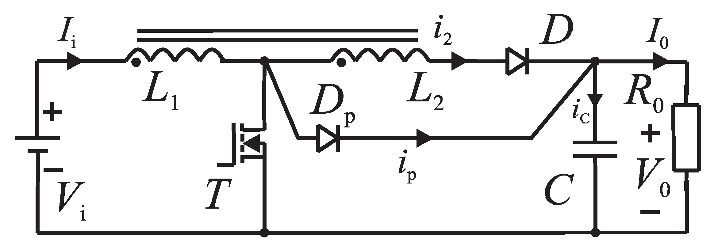
Figure 1. Topology of tapped-inductor step-up DC–DC converter.
Energies 17 04413 g001
Figure 2. The topology of multi-phase interleaved step-up DC–DC converter (left) and driving signals of 3-phase converter (right).
Energies 17 04413 g002
Figure 3. Single phase of the converter with parasitics.
Energies 17 04413 g003
Figure 4. PSpice model of 3-phase interleaved step-up DC–DC converter.
Energies 17 04413 g004
Figure 5. Step and frequency responses for n = 3 phases and D = 0.6 .
Energies 17 04413 g005
Figure 6. Step and frequency responses for n = 3 phases and D = 0.7 .
Energies 17 04413 g006
Figure 7. Step and frequency responses for n = 5 phases and D = 0.6 .
Energies 17 04413 g007
Figure 8. Step and frequency responses for n = 5 phases and D = 0.7 .
Energies 17 04413 g008
Figure 9. Parameters used to evaluate the results.
Energies 17 04413 g009
Table 1. Converter parameters.
ParameterSymbolValueUnit
Input voltage V i 40V
Primary winding inductance L 1 77 μ H
Turns ratioN 3.92 -
Coupling coefficientk 0.977 -
Primary winding resistance r 1 4m Ω
Secondary winding resistance r 2 110m Ω
Transistor T (STW88N65M5) on resistance R D S ( o n ) r T 30m Ω
Dynamic resistance of diode D (CSD10120) r D 75m Ω
Capacitor shunt resistance r C 50m Ω
Load capacitanceC60 μ F
Load resistance R o 127 (for n = 3 ) Ω
77 (for n = 5 ) Ω
Switching frequency f s 20kHz
Table 2. Step responses comparison (differences between considered mathematical models and the PSpice model).
ParameterUnitAveraged ModelSwitched Model
n = 3 , D = 0.6 and R o = 127   Ω
Δ V A 1 % 6.56 8.35
Δ V A 2 % 11.76 15.85
Δ V S S % 0.25 0.25
Δ t m a x ms 0.08 0.07
Δ t r i s e μ s 8.31 3.92
n = 3 , D = 0.7 and R o = 127   Ω
Δ V A 1 % 3.08 4.21
Δ V A 2 % 8.09 9.27
Δ V S S % 0.52 0.52
Δ t m a x ms 0.09 0.08
Δ t r i s e μ s 11.09 5.38
n = 5 , D = 0.6 and R o = 77   Ω
Δ V A 1 % 1.23 3.21
Δ V A 2 % 0.54 2.15
Δ V S S % 0.63 0.51
Δ t m a x ms 0.10 0.08
Δ t r i s e μ s 16.11 6.43
n = 5 , D = 0.7 and R o = 77   Ω
Δ V A 1 % 0.99 0.68
Δ V A 2 % 3.78 1.51
Δ V S S % 0.43 0.53
Δ t m a x ms 0.10 0.06
Δ t r i s e μ s 24.23 10.31
Disclaimer/Publisher’s Note: The statements, opinions and data contained in all publications are solely those of the individual author(s) and contributor(s) and not of MDPI and/or the editor(s). MDPI and/or the editor(s) disclaim responsibility for any injury to people or property resulting from any ideas, methods, instructions or products referred to in the content.