1. Introduction
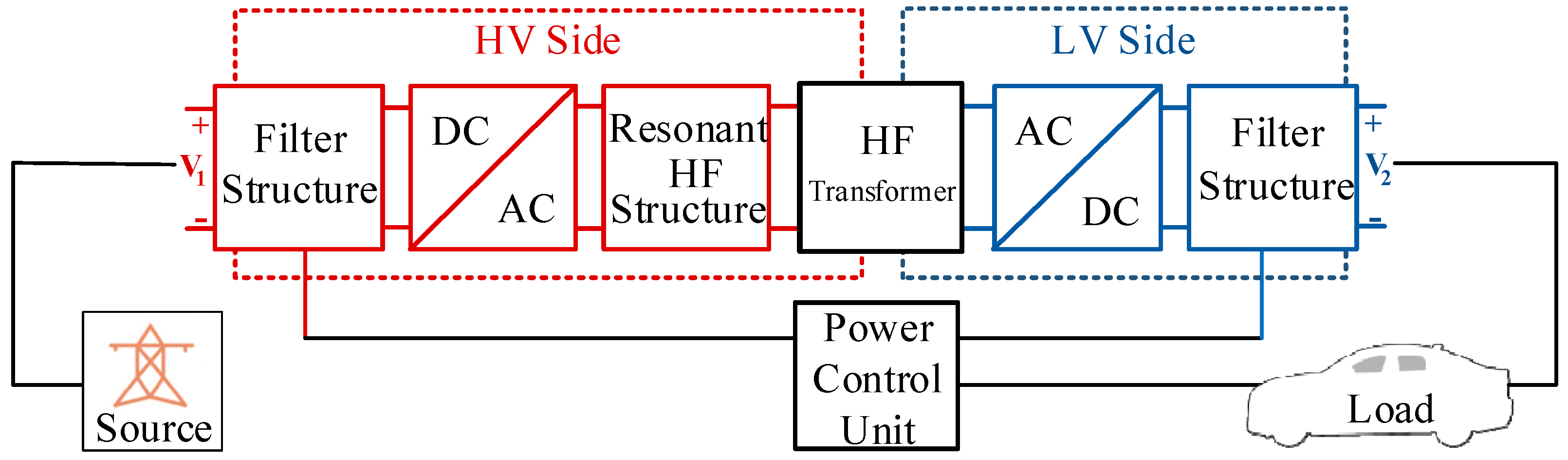
Bidirectional DC–DC converter topologies have become an attractive option in recent years, especially for renewable energy and electric vehicle technologies. The general block diagram of the elements included in galvanically isolated bidirectional DC–DC converter topologies is shown in
Figure 1 alongside the EV charging elements, which are shown in black. The details of the figure are as follows:
(a) The filter structure located at the input and output is used to obtain a smooth DC terminal voltage and current with no observable oscillations.
(b) The DC–AC converter consists of a structure made of semiconductor switch elements and is responsible for providing AC power to a high-frequency (HF) transformer operating from 20 kHz up to 350 kHz [
1,
2]. The AC–DC converter structure provides DC power to the respective input or output terminal using switches, typically ranging from 4 to 20 active components or switches [
2]. Both converters include elements that allow for bidirectional power flow. Typically, full-bridge, half-bridge, and push–pull circuit structures are used in these configurations. Moreover, the literature includes a bidirectional single-switch cross converter topology, as presented in [
3].
(c) The leakage inductances in the HF transformer provide energy storage capability in the AC part, altering the switching current waveforms and, thus, enabling low switching losses (up to %99+ efficiency). This structure is not necessary for every bidirectional DC–DC converter. Practically, these are shown as parasitic elements of the HF transformer.
(d) The HF transformer is required for electrical isolation. In addition to isolation, it provides a high voltage and current transfer ratio (ranging from 1:1 to 50:1). The HF transformer is more size efficient compared to low-frequency transformers [
2]. However, converter losses increase in high-frequency operating converters [
4]; hence, the most suitable switching frequency for the topology needs to be determined.
The isolated bidirectional DC–DC converter block diagram shown in
Figure 1 is referred to as a single-stage topology [
5]. These topologies consist of a minimum number of converter stages. The number of required elements is lower compared to other multi-stage topologies. Nevertheless, operating across a wide input and output voltage variation range can lead to the inefficient use of transformers and switch elements.
The effective use of transformers and semiconductor switches is achieved with multi-stage topologies, and these structures adjust the voltage and current levels by including additional power converters.
3. Modes of Operation
3.1. DAB Configurations
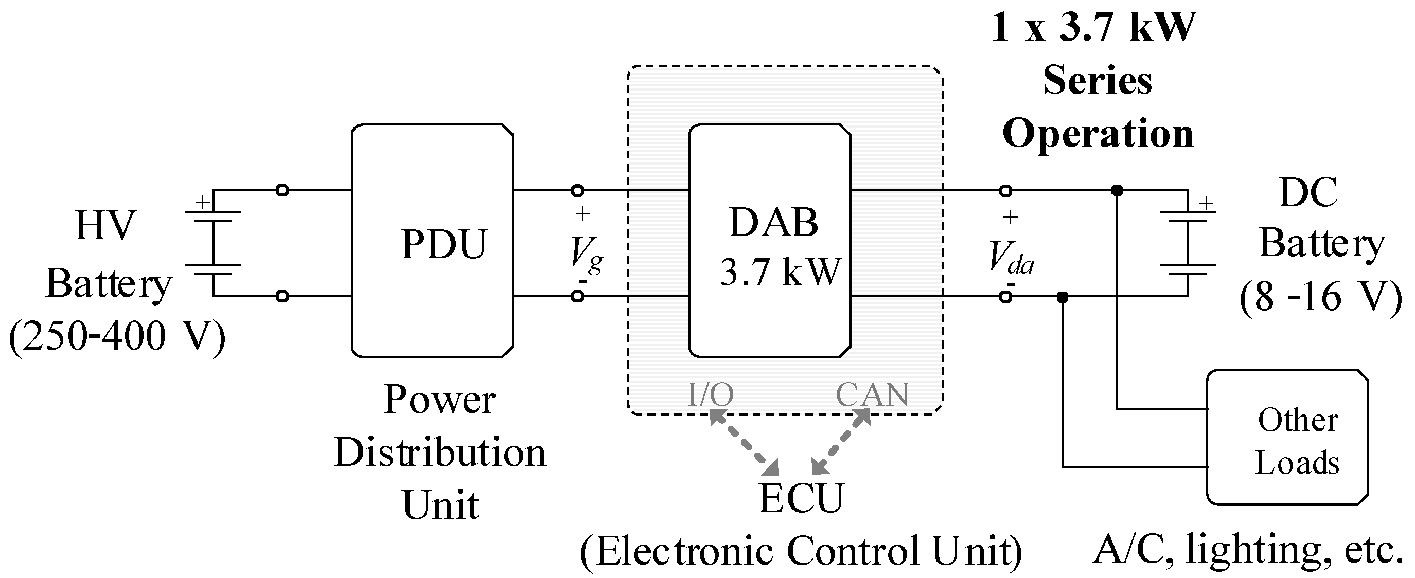
The advantages of the Dual Active Bridge (DAB), such as its ability to transfer power bidirectionally, perform soft switching over a wide voltage range, operate with numerous modulation techniques, and achieve high efficiency, make it an appealing choice for battery charging converters in both heavy and light electric vehicles. This study proposes a low-voltage battery charger converter for both heavy and light electric vehicles, utilizing a DAB topology with silicon carbide and silicon switches. The combined use of silicon carbide and silicon switches results in a highly efficient, high-power density, and compact converter [
26].
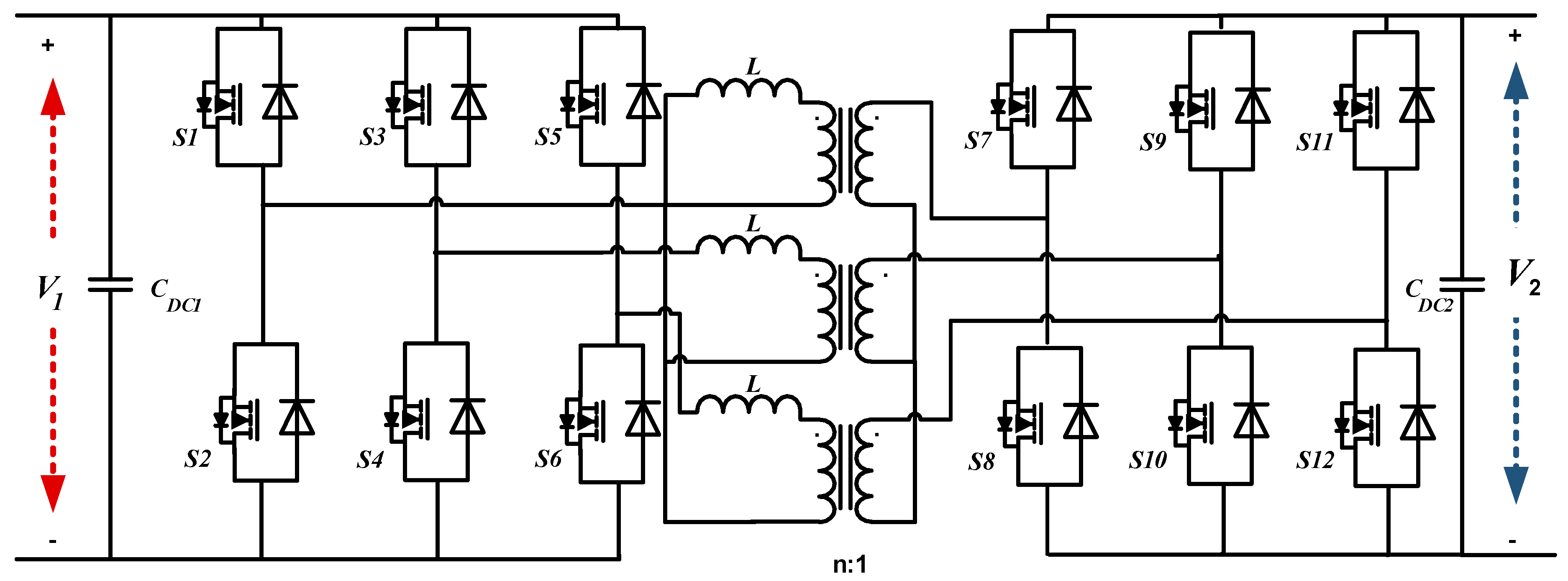
Two different converter configurations, each based on the main power structure of a 5.6 kW DAB converter, are illustrated in
Figure 8 and
Figure 9. As shown in the figures, the proposed converter can be used in various power values and applications. The nominal input voltage, output voltage range, and power values for the converters in
Figure 8 and
Figure 9 are provided separately in the figures. For heavy electric vehicles, a battery charger converter powered by a high-voltage battery ranging from 400 to 900 V and capable of 11.2 kW is shown in
Figure 8. The converter operates by interleaving two parallel DAB converters, each of 5.6 kW. It is designed to charge two series-connected 12 V batteries within a range of 16–32 V with a maximum output current of 200 A. On the other hand, the main 5.6 kW DAB converter is configured to be powered by a vehicle battery in the range of 250–400 V and to operate as a battery charging converter for light electric vehicles with a maximum power of 3.7 kW. In this scenario, the DAB converter will charge a single 12 V battery with a maximum output current of 260 A in the voltage range of 8–16 V. Both configurations can use a single DAB converter without any updates to the semiconductor power switches or magnetic circuit elements. Two different configurations for a low-voltage battery charger converter based on DAB topology are shown.
3.2. Alternative Power Stage Connections
3.2.1. Alternative Power Stage Connection-1 for 11.2 kW Heavy-Vehicle Converter
This configuration achieves operation by paralleling two 5.6 kW units and operating them in an interleaved manner, with the general block diagram provided in
Figure 10. To optimize the efficiency and maintain the temperatures of the MOSFETs on the AC side within appropriate ranges, three parallel MOSFETs are utilized, as discussed in [
27]. Thus, for a single 5.6 kW unit on the AC side, 12 MOSFETs are used, totalling 24 MOSFETs for the 11.2 kW converter. Each 5.6 kW unit uses a transformer with a single primary and a single secondary output.
Interleaved operation reduces the ripple current of the output capacitor, subsequently decreasing the capacitor’s value. The disadvantages of this alternative include the use of 24 MOSFETs, potential current-sharing issues among parallel MOSFETs, the challenge of driving parallel MOSFETs, and the difficulties in PCB design due to effective currents of 200 A passing on the secondary side of the transformer for each 5.6 kW unit.
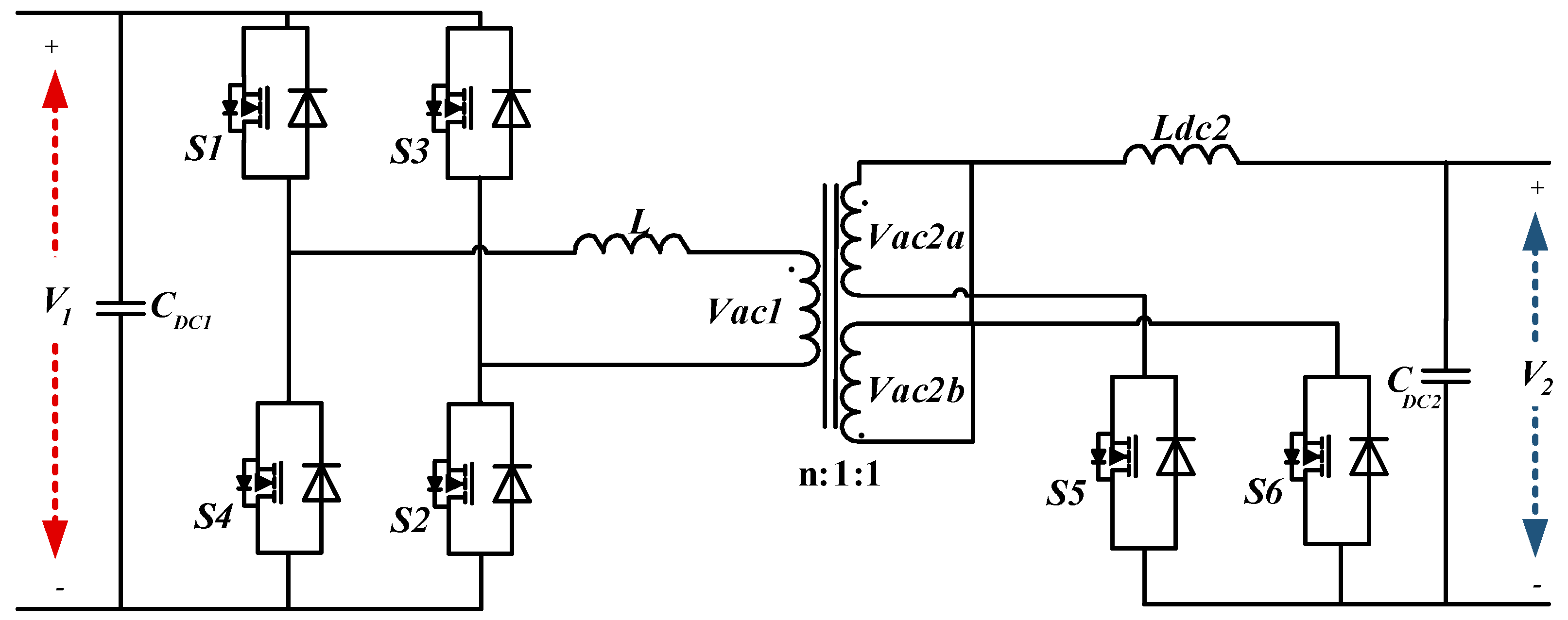
3.2.2. Alternative Power Stage Connection-2 for 11.2 kW Heavy-Vehicle Converter
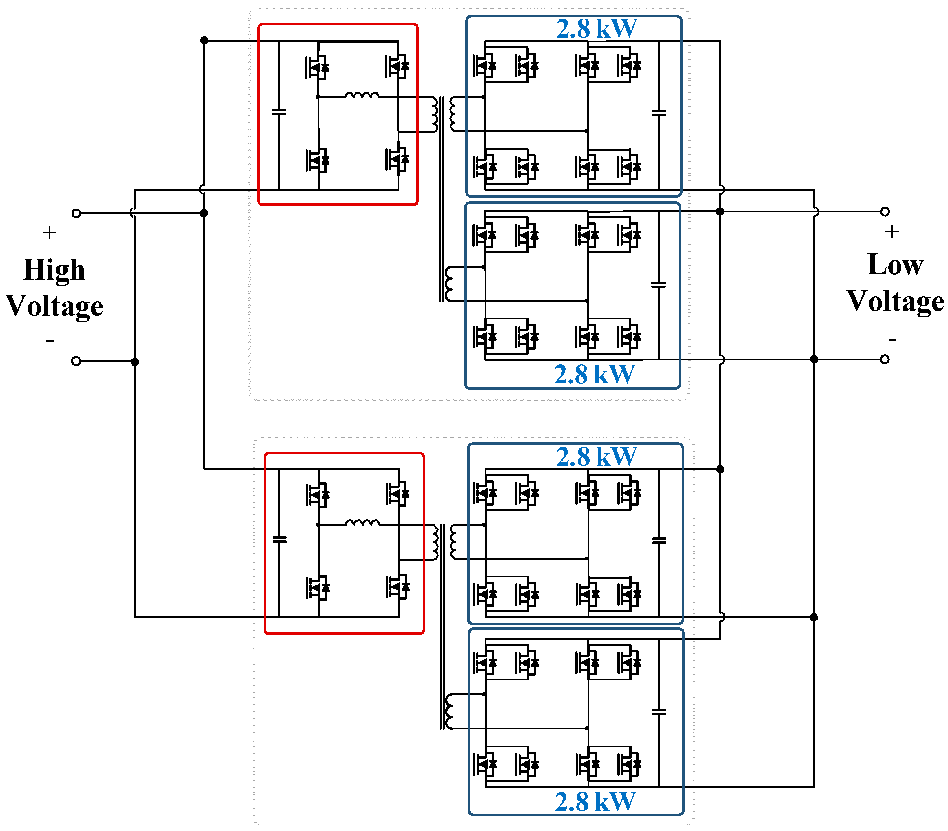
In this connection, each 5.6 kW unit’s transformer secondary output is doubled, designed to provide 2.8 kW per output, with the block diagram shown in
Figure 11. Since there is no need for paralleling in each 2.8 kW unit, only one MOSFET is used. Consequently, 8 MOSFETs are used on the AC side for each 5.6 kW unit, totaling 16 MOSFETs. This alternative uses eight fewer MOSFETs compared to the other option. The 2.8 kW units are paralleled among themselves, while the 5.6 kW units operate in an interleaved manner. The transformer used in this alternative has dual outputs, reducing each output’s secondary current to around 100 A, facilitating easier PCB design [
4]. Although the effective currents through the MOSFETs have increased compared to the previous alternative, they remain within the normal operating limits described in [
28].
The interleaved operation of the 5.6 kW units maintains the same output ripple currents as the previous alternative. The reduced number of MOSFETs, ease of driving, and simpler PCB design make this alternative more feasible. Dual secondary output of the transformer is possible but may complicate the design.
3.2.3. Power Solid Connection for 3.7 kW Light-Vehicle Converter
In this connection, the 3.7 kW converter’s output power is achieved by the parallel operation of two 1.85 kW output stages. To reach the targeted efficiency and ensure that the temperatures of the AC-side MOSFETs remain within appropriate ranges, two parallel MOSFETs are used. Thus, for the 3.7 kW unit, 16 MOSFETs are utilized on the AC side. Each 2.7 kW unit on the AC side will operate at a peak of 1.85 kW at full power. Since the DC side is single, interleaved operation is not possible; hence, the AC side operates in parallel.
The technical specifications of each converter (for heavy and light electric vehicles) shown in
Figure 9 are provided separately in
Table 2. As previously mentioned, the main power stage, a 5.6 kW DAB converter, can be used for both an 11.2 kW heavy electric vehicle operating in phase-shifted mode and a 3.7 kW light electric vehicle charger by merely changing the energy transfer inductor of the magnetic circuit elements.
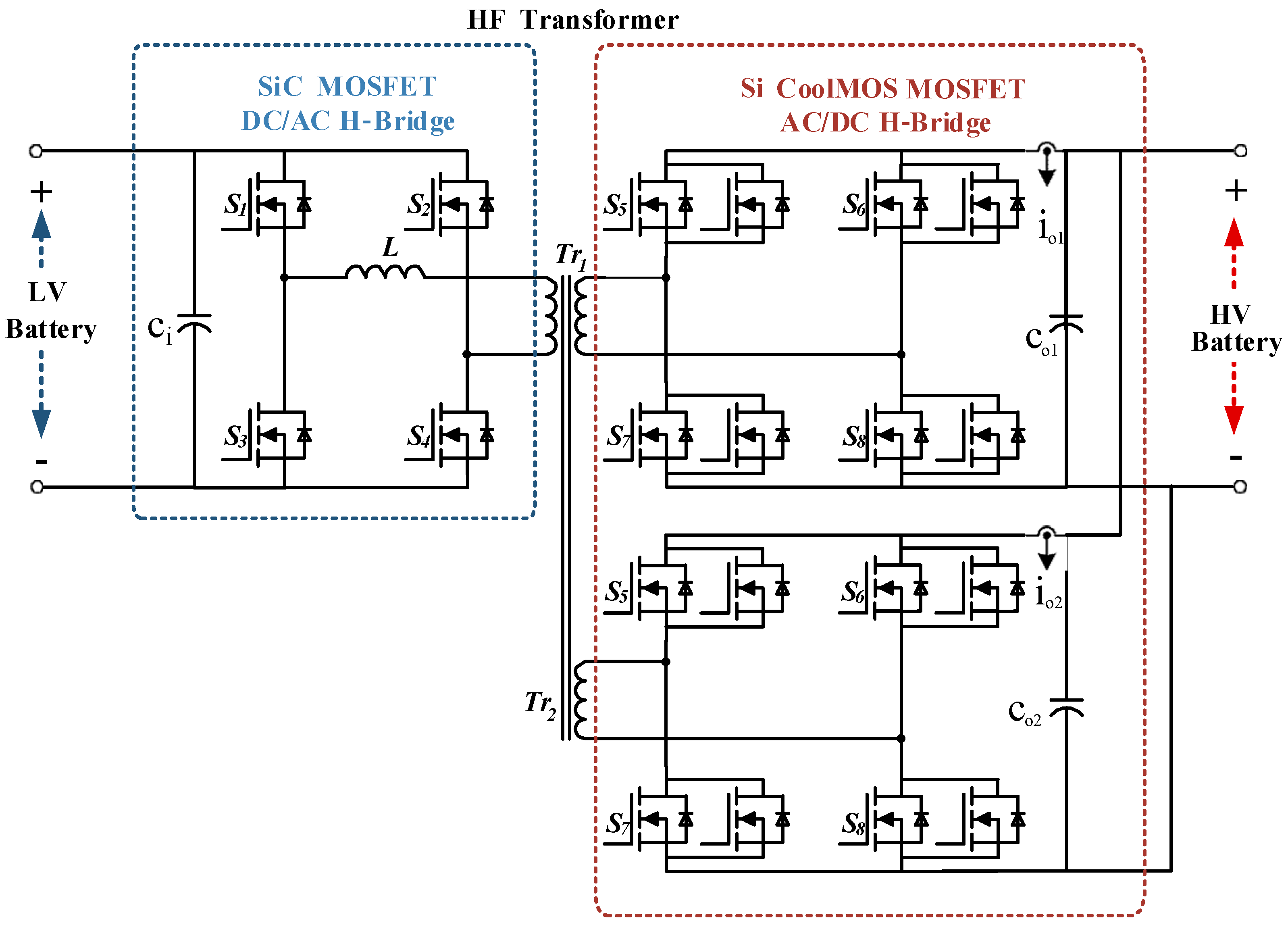
The main power board of the DAB converter is designed with a circuit board that can transfer power smoothly under the highest current condition of 260 A. The circuit of the main 5.6 kW DAB converter is given in
Figure 12.
For the high-voltage side, which is the input H-bridge circuit of the DAB converter, silicon carbide power MOSFET switches are used instead of silicon-based power MOSFET switches due to their superior low switching losses, high thermal stability, and high breakdown voltage. The use of silicon carbide switches allows the DAB converter to operate at a higher switching frequency, thereby reducing the size of passive and magnetic circuit elements in the circuit and increasing the power density of the converter. Moreover, the low output capacitors of silicon carbide switches reduce the energy required for soft switching, making soft switching easier to achieve.
On the other hand, silicon-based power MOSFET switches are used in the output stage of the DAB converter due to the low voltage on the secondary side. The conduction losses of the switches are dominant due to the high current on the secondary side. At this stage, the conduction resistances of silicon-based power semiconductors are lower compared to other switches, optimizing the design. To stay within a thermally safe range and further reduce the conduction resistance, the silicon-based switches in the H-bridge circuit of the output stage are used in pairs in parallel. The parallel H-bridge circuits on the secondary side of the DAB converter share the current equally under normal operating conditions. If equal current sharing is not achieved in the output-stage H-bridge circuit, unwanted currents will circulate between the bridges, increasing the losses of both the high-frequency transformer and the switches in the output stage, thus leading to thermal issues.
The filter capacitors on the input side and the capacitors capable of carrying high RMS currents in the output stage of the DAB converter can be significantly reduced when operating with phase-shifted switching of two 5.6 kW DAB converters. By the nature of the DAB topology, there is no filter inductor on the output, which results in high RMS ripple currents passing through the output capacitors and high voltage ripples on the output voltage also. This issue can be easily resolved with interleaved switching. For this purpose, the power stage switching of each DAB converter should be phased 180 degrees apart (for two DAB converters). This approach effectively cancels out the high-frequency ripple currents drawn from the input and output power stages, resulting in much lower levels. This, in turn, reduces the RMS current requirement of both the input and output capacitors, allowing for the use of commercially smaller capacitors.
3.3. DAB Operation Phases
In the DAB converter topology, power transfer occurs through appropriate phase shifting of the high-frequency square wave between two H-bridges. In its simplest form, these square waves are generated with a D = 1/2 duty cycle, and this method is referred to as the single-phase shift (SPS) technique. Power transfer occurs from the leading H-bridge to the lagging H-bridge, and the magnitude and direction of the transferred power can be easily controlled by changing the phase shift parameter.
The power transfer fundamentally occurs through the leakage inductance of the high-frequency transformer or an inductor externally added to the circuit. Due to the phase-shifted nature of the DAB converter topology, the inductor current and voltage follow each other with a certain delay, resulting in unwanted reactive currents circulating within the circuit or between the H-bridges. These currents increase both the current stress on the semiconductor switches and the copper losses in the high-frequency transformer.
Advanced modulation methods containing complex control techniques, such as dual-phase shift and triple-phase shift, can significantly reduce this reactive current problem. In this study, the single-phase shift modulation technique has been preferred and used for its ease of application.
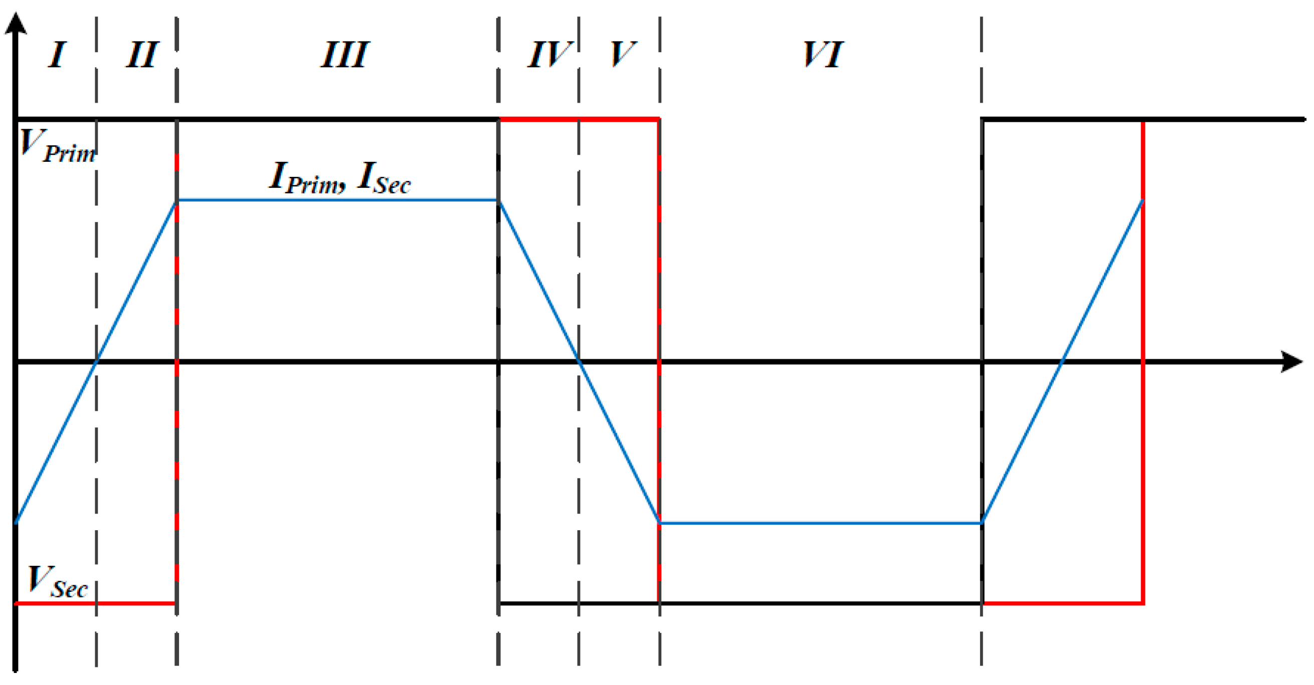
The voltage and current waveforms for these intervals are given in
Figure 13. The basic operating phases of the DAB converter are presented in
Figure 14. For clarity, the switching sequence is examined in six distinct intervals (four active).. In the first interval, the current through the energy transfer inductor changes from a negative to a positive value. During this interval, the primary side switches S1 and S4, and the secondary side switches S6 and S7 are conducting.
The voltage difference between the primary and secondary windings of the transformer is seen across the energy transfer inductor, and the slope of the inductor current during this condition is calculated, as shown in Equation (1). Besides the fundamental component of the energy transfer inductor current, high-order harmonic components are present due to the rise or fall times of the current during its increasing or decreasing moments. These high-frequency harmonic components increase the core losses of the inductor.
In the second interval, the inductor current is entirely positive, and while the primary side switches S1 and S4 continue to conduct, the secondary side switches S5 and S8 start conducting. Zero-voltage switching occurs in the dead-time region of this interval. The slope of the inductor current during this interval is given in the equation below:
In the third interval, the inductor current decreases from its peak value to a negative value. Due to the negative voltage across the inductor in this interval, the inductor current decreases with a negative slope, as shown in Equation (3). During this interval, while the secondary side switches S5 and S8 continue to conduct, the primary side switches S2 and S3 start conducting due to the negative voltage across them.
In the fourth interval, the inductor current continues to be negative and decreases with a negative slope, as shown in Equation (4). During this interval, the primary side switches S2 and S3 continue to conduct, while the secondary side switches S6 and S7, as in the previous interval, start conducting again.
As previously mentioned, during the transition from phase one to phase two, in the dead-time region, the energy charged on the energy transfer inductor discharges the output capacitors of the relevant MOSFETs and maintains their voltage at zero before they start conducting again. This phenomenon is referred to as zero-voltage switching (ZVS). One of the greatest advantages of the DAB converter becomes evident here. Due to the nature of the DAB topology, the delayed current stored in the inductor, caused by the phase difference between the two H-bridges, enables all switches in the lagging bridge to perform ZVS, while the switches in the leading H-bridge perform ZVS on one leg under all load conditions. ZVS depends on the load conditions at that moment and, hence, on the energy stored in the inductor. This allows the output capacitors of the MOSFET switches to be completely discharged.
Another important point is that the MOSFET power switches in the lagging H-bridge operate with synchronous rectification (through the MOSFET’s conduction resistance), while the MOSFET power switches in the leading H-bridge, according to the phase shift, mostly operate in forward conduction mode (through the body diode).
4. Design of the DAB Converter
In this section, computer simulation studies of the DAB converter have been conducted, and the operating conditions of the converter have been optimized according to different power levels, input voltages, energy transfer inductor inductance values, and phase shift values between converter voltages, as specified in
Table 3. Alongside these studies, switching and conduction losses of the power semiconductors to be used have been obtained through both theoretical calculations and simulation studies and compared.
The core material and winding design for the energy transfer inductor and the high-frequency transformer to be used in the AC link have been optimized to enhance the efficiency. The design of the transformer and inductor has been updated to be used in converters for both configurations, taking into account their current characteristics.
In electric vehicle converter applications, topology selection and power stage design are crucial but so are the volume, weight, and power density. The selection and design of power semiconductor switches and magnetic circuit elements have taken these factors into account to minimize cooling needs and optimize the efficiency.
The high-frequency transformer design for use in the AC link has been tailored to operate in both heavy and light electric vehicle converters. The HF inductor design has been optimized separately for each configuration to enhance the efficiency. Thus, components that are relatively challenging to design have been made to be commonly used across different configurations as much as possible, while components that are easier to design have been designed separately for different configurations.
4.1. Dual Active Bridge Simulation Studies and Power Semiconductor Analysis
Simulation studies for the 5.6 kW single unit converter, which can be more commonly used in both configurations, have been conducted using the MATLAB Simulink program based on the circuit provided in
Figure 12. Simulation studies for the DAB topology were first conducted using ideal switches and passive elements, followed by simulations with selections based on real commercial products.
To verify the accuracy of the proposed approach, we conducted simulations under various conditions, including extreme battery scenarios and realistic environments, which are described in this section. These simulations were then utilized with RT-LAB to perform hardware validation using our OPAL-RT system. The simulations were performed using MATLAB version 2022a and RT-Lab 2023.1 on a system running an Intel Core® i7™ 13650HX CPU at 2.6 GHz, with a 64-bit Windows 11 OS and 32 GB of DDR5 RAM with a frequency of 4800 MHz.
For this study, we utilized the OP5707XG RT-Laboratory from OPAL-RT, a real-time simulator fully integrated with MATLAB. The RT setup consists of two PCs: one as the host and the target PCs, connected via the TCP/IP protocol, which can be seen in
Figure 15. The OPAL-RT OP5707 XG is equipped with 64 fast input/output channels featuring DB37 and RJ45 connectors, with the latter being used in our configuration, design parameters can be found in
Table 3.
The general parameters of the circuit under simulation are provided in
Table 3 below.
Table 3.
Interleaved operation design parameters.
Table 3.
Interleaved operation design parameters.
| Technical Specification | Value |
|---|
| Nominal input voltage (V) | 750 |
| Nominal output voltage (V) | 28 |
| Nominal output power (W) | 5600 |
| Output impedance (Ω) | 0.14 |
| Switching frequency (kHz) | 50 |
| HV MOSFET voltage (V) | 1200 |
| HV MOSFET current (A) | 120 |
| LV MOSFET voltage (V) | 80 |
| LV MOSFET current (A) | 180 |
| Transformer turns ratio (n) | 30:1:1 |
| Bridge inductor value (μH) | 150 |
| Output capacitor (mF) | 12 |
| Output capacitor ESR (mΩ) | 2.2 |
The amount of power to be transferred by the DAB circuit topology, neglecting harmonics, is calculated as shown in the following equation:
Here,
V1 represents the effective value of the transformer primary winding voltage,
V2 represents the effective value of the voltage on the output side of the energy transfer inductor,
XL represents the reactance value of the energy transfer inductor at the switching frequency, n represents the transformer turns ratio, and θ represents the phase shift value on the AC side. According to Equation (5), the amount of power transferred varies depending on the amplitude of the square-wave signal in both H-bridge circuits, the value of the energy inductor, and the sine of the phase difference between the AC-side voltage and the DC-side square-wave voltage. For a phase shift value of 36°, the driver signals for the MOSFET switches on both the AC and DC sides are shown in
Figure 16:
Assuming the inductor value is fixed after the design phase, the parameter controlling the changing power or voltage values is the phase shift value between the two H-bridges.
Figure 16 shows the AC- and DC-side MOSFET driver signals. The phase shift value varies between 0° and 360°, and after 180°, the direction of power flow changes.
Figure 17 shows the voltage waveforms at the inductor input and output and the inductor current waveform after the applied phase-shifted signals:
As seen from Equation (5), the amount of transferred power increases as the phase shift value increases.
4.2. Power Semiconductor Loss and Conduction Losses for the DC Side
Power semiconductor losses for a single 5.6 kW DAB converter unit are given in this section. Discrete package silicon carbide switches have been used for the high-voltage H-bridge switches. The silicon carbide switch has a typical conduction resistance of 25 mΩ at 1200 V and 60 A voltage and current values.
When the silicon carbide switch is driven at V
gs = 20 V, according to the simulation result in
Figure 18, the drain-source current Ids is approximately 8 A rms. Using the conduction resistance R
ds of approximately 43 mΩ provided in the datasheet for the worst-case scenario, the MOSFET drain-source voltage is approximately V
ds = 0.4 V. Therefore, the conduction loss value for each switch in the input H-bridge circuit of the converter is 3.2 W, totaling 12.8 W for the entire H-bridge. The conduction loss for each MOSFET based on the simulation result is shown in
Figure 19. As can be seen, the calculated conduction loss value is approximately the same as that of the simulation results.
4.3. Switching Losses
With the input DC voltage of the converter H-bridge at 800 V and the silicon carbide switch drain-source current
rms, the total switching loss energy according to the switch datasheet is 0.3 mJ. Thus, the switching loss value for each switch in the input H-bridge circuit of the converter is 15 W, making the total H-bridge switching loss 60 W. The calculated switching losses for each switch during conduction and turn-off match the simulation results. The simulation results are shown in
Figure 20 and
Figure 21, respectively:
Consequently, the total loss for the switches on the input side of the converter is calculated as 72.8 W.
Figure 19 shows the simulation result for switching loss during conduction for the input H-bridge silicon carbide switch.
Figure 21 shows the simulation result for switching loss during cutoff for the input H-bridge silicon carbide switch.
4.4. Power Semiconductor and Conduction Loss Calculations for the AC Side
Discrete package silicon switches with very low on-resistance values have been used for the low-voltage H-bridge switches. Since much higher currents flow through the converter’s output stage compared to the input stage, the conduction losses, and therefore the drain-source resistance, become very significant. Each switch in the output H-bridge circuit is used in a three-parallel configuration to further reduce the on-resistance and minimize conduction losses. The easy paralleling capability of silicon MOSFET switches also provides an advantage for the application. The selected silicon switch has a typical on-resistance of 1.9 mΩ with voltage and current ratings of 80 V and 180 A, respectively.
When the silicon switch is driven at
, the simulation results are as shown in
Figure 22.
The drain-source current
rms. Using the on-resistance
provided in the datasheet for the worst-case scenario, the MOSFET drain-source voltage is approximately
. Therefore, the conduction loss value for each switch in the output H-bridge circuit of the converter is 9.3 W, making the total H-bridge conduction loss for all 12 switches 112 W. The simulation result for the drain-source voltage of each MOSFET is shown in
Figure 23 below.
4.5. Switching Losses
With the output DC voltage of the converter at 28 V and the drain-source current value of each silicon switch
rms, the total switching loss energy according to the switch datasheet is 0.01928 mJ. Thus, the switching loss value for each switch in the output H-bridge circuit of the converter is approximately 1 W, making the total H-bridge switching loss for 12 switches 12 W. The conduction loss simulation results for each MOSFET are shown in
Figure 24 and
Figure 25, respectively. According to conduction and switching losses, the total loss for the silicon switches in the output stage is 124 W.
It is important to note that the conduction losses of the output silicon switches are significantly higher than those of the input silicon carbide switches. As the drain-source resistances change with temperature, the drain-source resistance should be recalculated based on the realistic operating condition temperature provided in the switch datasheet, and the switch losses should be reassessed for this worst-case scenario. If it is assumed for this study that the operating temperature of the output silicon MOSFET switches is 100 °C, the on-resistance would be approximately , making the total conduction loss 136 W. With the updated , the total power loss for the output stage switches is 148 W.
Determining the Optimal Value of the Energy Transfer Inductor
To enable the converter to operate under various load and input voltage conditions, it is necessary to determine the optimal value of the energy transfer inductor. The converter must be able to deliver maximum current values between the minimum and nominal output voltages, and power transfer should be limited when the output voltage exceeds the nominal voltage. As seen in
Figure 9, the minimum output voltage is 16 V, at which the converter must deliver a total output current of 260 A. In this condition, the input voltage is 450 V. The phase angle for the converter’s operating conditions will be determined at this operating condition. As understood from Equation (5), the value of the phase angle varies significantly for input voltages of 750 V and 450 V when the inductor value and power are fixed. This helps determine the limits of the phase angle.
Another important point is that to operate at the same power point, an increase in the phase shift value requires an increase in the inductor value, as illustrated on
Figure 26. Additionally, increasing the inductor value leads to an increase in the output capacitor ripple currents, thus necessitating a larger capacitor value.
Figure 27 illustrates the change in the inductor value corresponding to the phase shift change at the same power level (11.2 kW).
Figure 27 shows the change in the effective value of the output capacitor current as the inductor value increases.
When simulation studies are conducted, the inductor value to be used on the primary winding side of the transformer is 150 μH, and the phase value is around 16°. Moreover, the results obtained from simulations for different power and input voltage values are summarized in
Table 4. As seen in
Table 4, for the worst-case scenario with an input voltage of 450 V, the phase shift needs to be around 85° to transfer 5.6 kW of power. Another point noted in
Table 4 is the increase in the output capacitor ripple current as the inductor value is raised for a power value of 11.2 kW.
Reducing the inductance value too much causes the phase angle value at full power to decrease, leading to very small angle values at lower powers and affecting control precision adversely.
For the selection of capacitors in the input and output stages of the DAB, we converter considered the following factors:
Ripple current carrying capacity;
ESR and ESL values;
Maximum operating temperature value;
Resistance to environmental conditions such as humidity and vibration;
Availability for automotive applications;
Size and volume;
Weight.
Especially since there is no filter inductor in the output stage of the DAB converter, the bus capacitor is exposed to high RMS ripple currents, and choosing an appropriate capacitor value is crucial for the operation of the converter.
Upon examining Equation (5), it is evident that the factors affecting the RMS value of the output capacitor current are as follows:
These two values determine the power the DAB converter will transfer to the load and, consequently, the output current and capacitor ripple current. Inserting the nominal operating values from
Table 4 into Equation (5) yields the values in
Table 5.
Table 5 shows the inductance value based on the phase shift value as a reference. The maximum limit of the phase shift value for power transmission from the DC to the AC side is 90°. At this value, the output power is maximized and then decreases again up to 180°. Beyond this value, the direction of power flow changes. To avoid approaching the limit value too closely and because the capacitor ripple current increases as it approaches the limit values, the phase shift starting value is chosen as 72°. Selecting a higher phase shift allows for more precise control of the output voltage over a wider range.
Figure 28,
Figure 29,
Figure 30 and
Figure 31 show the output capacitor voltage waveform and effective current value for phase shift values of 36° and 72°, respectively. When the phase shift value is halved and the inductance value is calculated using Equation (5), the output capacitor ripple current is seen to be nearly halved. This result is considered more reasonable in terms of converter sizes and capacitor temperature values. When examining commercial products, it is observed that the output voltage ripple value has a wider range; hence, lower capacitor values are used.
Simulations for nominal operating conditions were conducted with an output capacitance value of 3 mF and an ESR value of 3 mΩ. For both phase shift angles, the converter output voltage ripple value (peak to peak) is smaller than the targeted 280 mV (1% of the nominal output voltage). The effective value of the output capacitor current is 110 A for a phase shift angle of 36° and 200 A for a phase shift angle of 72°. According to these results, an electrolytic or metal film-type capacitor with a capacity value of 3 mF, an equivalent series resistance of 3 mΩ or lower, and a 100 A rms current carrying capability are required for the DAB converter output capacitor. Commercial products for metal film capacitors at these capacity values are very limited and occupy a lot of volume when used in parallel. Therefore, electrolytic-type capacitors, which have higher energy densities and relatively smaller sizes, are preferred in this study.
The selected capacitor is of the aluminum electrolytic type, designed for automotive applications, capable of operating up to 150 °C, and resistant to vibrations. It has a high ripple (ripple current) carrying capacity and low ESR values. In the simulation studies, the energy transfer inductor was initially used on the secondary side of the transformer and later moved to the primary side. The calculations for capacitor selection assumed an operating temperature of 105 °C. In this study, aluminum electrolytic capacitors with a capacity value of 7.2 mF, an equivalent series resistance of 2.2 mΩ, and a 147 A rms current carrying capability were selected.
5. Experimental Results and Discussion
The experimental results of the designed 50 kHz, 5.6 kW DAB converter are presented under this heading. The first section provides a visual of the converter, while the subsequent section shares the experimental results showing the converter’s performance and presents the efficiency graph under different load conditions.
The power stage and general unit view of the designed converter are shown in
Figure 32. Basically, it consists of a single-phase H-bridge circuit based on silicon carbide switches at the input stage, a high-frequency inductor, a high-frequency transformer, an output rectifier circuit with silicon switches, and aluminum electrolytic-type output capacitors, along with a breadboard to contain the programmable PIC18F67K22 microcontroller.
The performance of the developed DAB converter was tested in a laboratory environment to verify soft switching, a soft start, equal current-sharing control, thermal stability, and the overall efficiency of the system. The experimental results obtained are presented under this heading. Firstly, the converter output voltage and the current waveforms of the energy transfer inductor for the soft-start control applied to the 14 V vehicle battery of a light electric vehicle are shown in
Figure 33.
The purpose of the soft-start control is to prevent the capacitors with a high energy capacity on the output board from drawing sudden high currents when the nominal voltage is applied to the converter input, thereby protecting the circuit components from potential disruptive effects. Since there is no filter inductor at the output of the DAB converter, high capacitance values are used to keep the output voltage ripple below a certain level. Therefore, a soft-start technique is necessary to prevent these capacitors from drawing high inrush currents initially. The soft-start technique in this study is implemented by phase shifting within the H-bridge switches on the primary side. During the soft start, the MOSFET switches on the secondary side are in the cutoff state, and only the body diodes are conducting, making it function like a full-bridge rectifier circuit.
A proportional–integral control technique is used for soft-start control, preventing the input current from reaching high values until the output capacitors reach the appropriate voltage level. As seen in
Figure 33, the peak-to-peak current value through the inductor during the soft start is 12 A. Several different current waveforms in
Figure 33 result from the flat power region where no increase in the output power is observed despite the increase in the phase shift between the bridges, as previously mentioned. It takes approximately 6 s for the output voltage to reach the set value of 14 V. This duration can be shortened with higher inrush currents by changing the values of the proportional–integral controller.
The waveforms of the primary and secondary voltages of the transformer and the inductor currents at half load are shown in
Figure 34; at this moment, the DC currents in each parallel H-bridge on the secondary side and the output voltage are also shown in
Figure 35.
As seen from the inductor current waveform in
Figure 35, the converter is operating in buck mode, and due to the current being positive in the regions marked in green, both the primary and secondary side switches are performing zero-voltage switching. Since the inductor current is symmetrical for one switching cycle, the switches on the secondary side operate with minimal switching losses. The voltage gain of the DAB converter in
Figure 35 is approximately M = 0.9.
When the voltage gain of the DAB converter is one or greater, the MOSFET switches on the secondary side of the converter experience high switching losses during cutoff periods. Therefore, the value of the converter’s voltage gain is of great importance both in terms of losses and efficiency under normal operating conditions. On the other hand, when the voltage gain of the converter is less than one, the MOSFET switches on the primary side are exposed to high switching losses. However, due to the lower current values on the primary side and the low switching losses of the silicon carbide switches, this disadvantage is much lower compared to the Si MOSFET switches on the secondary side.
The current-sharing graph between the parallel H-bridges on the secondary side of the converter is shown in
Figure 35. As can be seen, current sharing between the H-bridges is very close to ideal conditions. The current-sharing difference between the H-bridges is less than 5% for a half load. Equal current sharing is designed to control the DC current in each parallel branch with a proportional–integral controller to reduce the current difference to zero. To prevent excessive current from flowing through a single branch, the converter is shut down as a safety measure if current sharing exceeds 10%.
Figure 35 also shows the soft-start region and the flat power region. As can be seen, in the flat power region, despite the increase in the phase shift value, the output current remained the same up to a certain level and then increased to the desired value.
The same voltage waveforms were taken for the boost mode under half-load conditions and are shown in
Figure 36. As seen in
Figure 36, although the inductor current is positive, zero-voltage switching could not be achieved due to the voltage gain being greater than one. The hard switching waveform resulting from the primary side switches not fully discharging their output capacitors is clearly visible in
Figure 36. On the other hand, due to the boost operating mode, the switches on the secondary side also experience high switching losses during cutoff. Based on the waveforms in
Figure 34 and
Figure 36, the battery voltage, current, and state of charge characteristics should be calculated for the most suitable converter design and efficiency:
For the case where the DAB converter is used for a heavy electric vehicle, different load characteristics result in different operating conditions. For example, in a typical heavy electric vehicle, the power drawn from the high-voltage battery under normal operating conditions is approximately 1.4 kW. This 1.4 kW power is consumed for general needs such as the air conditioning, lighting, and dashboard power of the electric vehicle under normal operating conditions. As mentioned, the converter delivers approximately 1.4 kW of power by supplying 50 A current to the 28 V battery under normal operating conditions.
The efficiency of the DAB converter, both theoretically calculated and experimentally measured, is plotted against the output power, as shown in
Figure 37. The test conditions applied for the efficiency values are also provided on the same graph. As seen from the efficiency graph, the converter achieves its maximum efficiency at approximately half-load conditions, measured at 98%. From half-load conditions onwards, the switching losses of the output power MOSFET switches become significant. For full-load conditions, the converter’s efficiency is measured at 97%. The overall efficiency of the converter is measured at 90% for conditions under a 10% load. While the conduction losses of the switches are significant up to a half load, the switching losses of the switches become significant for efficiency values between half-load and full-load conditions.
Due to the high currents that the converter output switches are subjected to, the voltage gain of the converter in its current operating condition plays a very important role in the losses and, consequently, in the efficiency. As can be seen, the selection of appropriate power semiconductor MOSFET switches for both the high-voltage and low-voltage sides of the DAB converter; the selection of materials, conductors, and proper winding techniques to minimize magnetic circuit element losses; and an appropriate control method result in a converter design that is both galvanically isolated and capable of operating at relatively high efficiencies. With these efficiency values, the current DAB converter design is competitive in terms of both the literature and commercial products.
6. Conclusions
In our study, a generalized DAB topology-based converter was designed and implemented for either a 750–28 V, 2 × 5.6 kW heavy electric vehicle or a 400–14 V, 3.7 kW low-voltage battery charging for a light electric vehicle. Silicon carbide power MOSFET switches were used on the high-voltage H-bridge side of the converter, while silicon CoolMOS-based power MOSFET switches were used on the low-voltage side. By operating two DAB converters alternately, power levels of up to 2 × 5.6 kW can be achieved. With appropriate switching and design parameters, the high-voltage H-bridge switches perform zero-voltage switching, while the low-voltage H-bridge switches perform zero-current switching.
For the applied DAB converter, an efficiency of 97% under full-load conditions and 98% under half-load conditions was achieved at a switching frequency of 50 kHz. The use of a microcontroller for the converter power stage design, the planar design of the high-frequency transformer, and the design of the high-frequency inductor ensured the high efficiency of the DAB converter.
Improvements and Future Work
Thermal management: While the study successfully mitigates conduction and switching losses, thermal management remains a critical area for improvement. Future work could explore advanced cooling solutions or heat sink designs to further enhance the efficiency and extend the converter’s lifespan.
Integration of GaN semiconductors: The promising characteristics of Gallium Nitride (GaN) semiconductors include their higher efficiency, faster switching capabilities, and lower intrinsic capacitance than SiC. These characteristics result in significantly faster switching speeds, reduced conduction losses, and higher efficiency, making GaN-based devices increasingly attractive for high-performance power converters. GaN components could be explored in future iterations of the converter design. This could potentially lead to further reductions in size and losses.
In the context of this converter design, integrating GaN technology could pave the way for more compact and lightweight solutions. GaN’s ability to operate at higher frequencies with minimal losses allows for smaller passive components, such as inductors and capacitors, contributing to overall reductions in the converter size and weight. Furthermore, the reduced thermal management requirements due to lower heat dissipation can lead to simpler and more efficient cooling systems, further enhancing the system’s overall reliability and longevity.
Advanced control strategies: Implementing more sophisticated control algorithms, such as adaptive phase shift control, could dynamically optimize the converter’s performance across a wider range of operating conditions, improving its efficiency and power density.
Modular design for scalability: Developing a modular converter design could facilitate scalability and customization for various EV charging applications, ranging from residential to commercial and fast-charging stations.
Integration with renewable energy sources: Future studies could explore the integration of DAB converters with renewable energy sources, enhancing the sustainability of EV charging infrastructure. This includes optimizing the converter for variable input sources such as solar or wind power.


