Article

In-Plane Liftout and Push-to-Pull for In Situ Mechanical Testing of Irradiated Inconel X-750

1
Idaho National Laboratory, Idaho Falls, ID 83415, USA
2
Department of Nuclear Engineering, North Carolina State University, Raleigh, NC 27695, USA
*
Author to whom correspondence should be addressed.
Energies 2024, 17(17), 4199; https://doi.org/10.3390/en17174199
Submission received: 23 July 2024 / Revised: 8 August 2024 / Accepted: 16 August 2024 / Published: 23 August 2024
(This article belongs to the Section B4: Nuclear Energy)

Abstract

:
A streamlined sample preparation method for nanomechanical testing is needed to improve the quality of specimens, reduce the cost, and increase the versatility of specimen fabrication. This work outlines an in-plane liftout focused ion beam (FIB) fabrication procedure to prepare electron-transparent specimens for in situ transmission electron microscopy (TEM) nanomechanical testing. Ion etching and electron backscatter diffraction (EBSD) techniques were used to lift out a [110] oriented grain from a neutron-irradiated bulk X-750 alloy. Careful control of voltages and currents ensured precision. Top surface thinning sweeps prevented resurfacing and redeposition while dog-bone geometries were shaped with a 1:4 gauge width-to-milling pattern diameter ratio. Nanotensile testing in the TEM with a picoindenter allowed for the estimation of an ultimate tensile strength of 2.41 GPa, and inspection revealed a high density of bubbles in the X-750 matrix. The proposed fabrication procedure is significant for preparing samples from radioactive materials, studying complex structures that are orientation-dependent, and analyzing desired planar areas.

1. Introduction

Thorough investigation into the mechanical and structural properties of a material on the micro to nano scale necessitates meticulous preparation of samples for testing. The procedures employed in sample preparation significantly influence the accuracy, reliability, and repeatability of test results [1,2]. Diligent sample preparation is essential to ensure that the data collected accurately represent the bulk material and to minimize variables and artifacts that could distort the intrinsic properties of the material.
For alloys and compounds utilized as structural materials, it is crucial to continually characterize and evaluate them over their lifetimes to comprehend their behavior under the harsh conditions within nuclear reactors [3]. The stringent requirements for materials used in nuclear reactor components emphasize the necessity for optimized, accident-tolerant, and cost-effective options [4,5,6]. Inconel X-750, employed in Canada Deuterium Uranium (CANDU) [7] pressurized heavy-water reactors as spacers between the hot pressure tube and the calandria tube, exemplifies such a material. This Ni-based precipitation-hardened superalloy is subjected to highly degradative conditions, including high temperature, elevated pressure, intense radiation, and corrosive environments [8,9]. Despite numerous studies demonstrating its remarkable material properties such as high-temperature resistance and acceptable creep tolerance [10,11,12,13,14], further exploration into the root causes of failure mechanisms upon reaching the end of service in the fuel channel is needed to understand the microstructural changes it undergoes following prolonged use in CANDU reactors. Therefore, an opportunity appears to develop a procedure that can produce high-quality samples to offer insights on X-750’s properties while conducting in situ experiments.
In situ nanotensile testing serves as a versatile technique for analyzing the microstructural changes and mechanical behavior of materials [15,16,17,18,19,20,21]. Moreover, preparing samples from the bulk X-750 superalloy at this scale requires utilizing a focused ion beam (FIB) coupled to a scanning electron microscope (SEM) to fabricate and affix specimens onto commercialized push-to-pull (PTP) devices to conduct the micro- and/or nano-mechanical experiments.
In this work, we developed a method for fabricating in-plane liftouts of irradiated X-750 superalloy, aimed at facilitating post-irradiation examination (PIE) and tensile testing. This method outlines an efficient approach for extracting the desired planar surface area from a grain with a specific orientation, addresses mitigation strategies for handling radioactive materials during sample preparation, and exhibits bubbles and dislocations in the microstructure. Our approach diverges from conventional 2D materials research as it begins with bulk sample preparation. Additionally, we employed electron backscatter diffraction (EBSD) and transmission electron microscopy (TEM) techniques to characterize the irradiated X-750 superalloy, enabling the correlation of radiation damage across grain orientations. Ultimately, our procedure yielded valuable insights, allowing for the identification of bubbles and dislocations during TEM imaging and the calculation of the mechanical properties of the alloy.

2. Materials and Methods

2.1. Materials

The chemical composition of the X-750 superalloy used for this study is listed in Table 1. The X-750 was used as an internal spacer to maintain gaps between hot pressure tubes in the CANDU reactor, which has highly thermalized neutron spectra and generates high production of helium [22]. After service, some X-750 samples were extracted, sectioned, and then shipped to the Irradiated Materials Characterization Laboratory (IMCL) at Idaho National Laboratory (INL) for PIE characterization. In this study, the examined X-750 material was extracted from a location in contact with the hot pressure tube where the specimens were irradiated between 300 and 330 °C. The displacements per atom (dpa) of the examined specimen was calculated using the industry-standard SPECTER code [23], which considered all the reactions that could induce atomic displacement for all the major alloying elements and provided helium generation rate data. The currently examined X-750 material (sample ID code: 11-CNL-019) was irradiated at about 325 °C to ~67 dpa with a neutron flux of 1.4 × 10 14 n/cm·s. The achieved helium content was calculated to be ~21,283 appm. The sample cross section was about 0.7 × 0.7 mm2.
Some limitations arise when dealing with highly radioactive samples. For instance, the user handling the material must minimize the time of exposure to receive the lowest dose possible. This requires that the procedure to mount the sample into a holder and the loading/unloading of the FIB stage be carried out swiftly. It is also important for the users to be as far away as possible and behind shielding when handling radioactive materials. Thus, the use of mechanical arms, gloveboxes, and long-range tools is needed, which complicates the sample preparation process. Skillful and properly trained scientists from IMCL loaded, unloaded, and transferred the irradiated Inconel X-750 material into the gloveboxes and electron microscopes used in this work.

2.2. Methods

The sample preparation was carried out in the following manner. First, the X-750 sample was loaded onto the G4 Helios plasma-focused ion beam-scanning electron microscope (FIB-SEM) DualBeam instrument for ion etching and EBSD mapping to locate the [110] oriented grains. Ion etching and EBSD techniques were employed to achieve a clear view of the grain topology. Etching removes any contamination and a few atomic layers by rastering the surface with the ion beam, revealing the grain boundaries and other intrinsic features of the sample. EBSD mapping provides detailed information on the crystallographic orientation of the material. The combined use of these techniques was crucial for identifying grains with the desired orientation and size, facilitating the selection of the area of interest and ensuring that the in-plane liftout extracted was indeed a [110] oriented grain. The [110] grain orientation was desired for optimal visibility of potential bubble–dislocation interactions and to minimize the need to tilt the TEM holder.
The EBSD map of a selected area is shown in Figure 1, where a grain of [110] orientation is highlighted. After identifying the desired grain, the X-750 material was transferred to a Quanta FIB-SEM to obtain the in-plane liftouts and attach them to PTP devices. The detailed procedure for this step will be reported in Section 3.1.
To perform the in situ testing, the PTP device with a prepared specimen was mounted onto a Hysitron PI95 picoindentation holder and then loaded into the Titan Themis TEM. Mechanical testing was conducted with a 100 µm flat diamond tip. The tensile experiment was performed at room temperature (RT) with a displacement control set to 1000 nm for 1 min, corresponding to a loading rate of approximately 16.7 nm/s. Continuous visual monitoring was needed as the experiment unfolded to capture images of regions of interest and record the procedure. Further TEM inspection of the X-750 matrix sample was employed to search for any microstructural defects, namely bubbles and dislocations. Additionally, electron energy-loss spectroscopy (EELS) measurements were collected with the TEM to estimate the thickness at the tensile testing area (necking region). The accelerating voltage of the TEM was 200 kV, the convergence angle was 50 mrad, and the collection angle was 150 mrad. These angles apply solely to EELS data collection.

3. Results

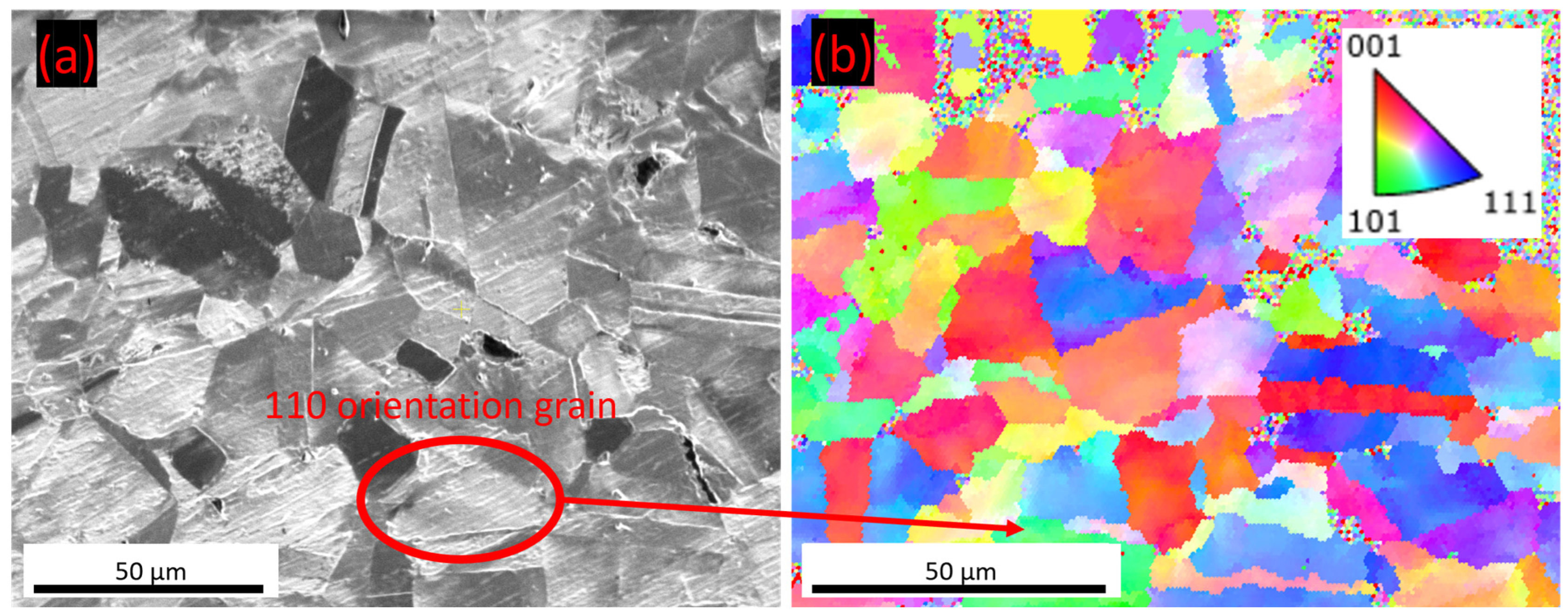
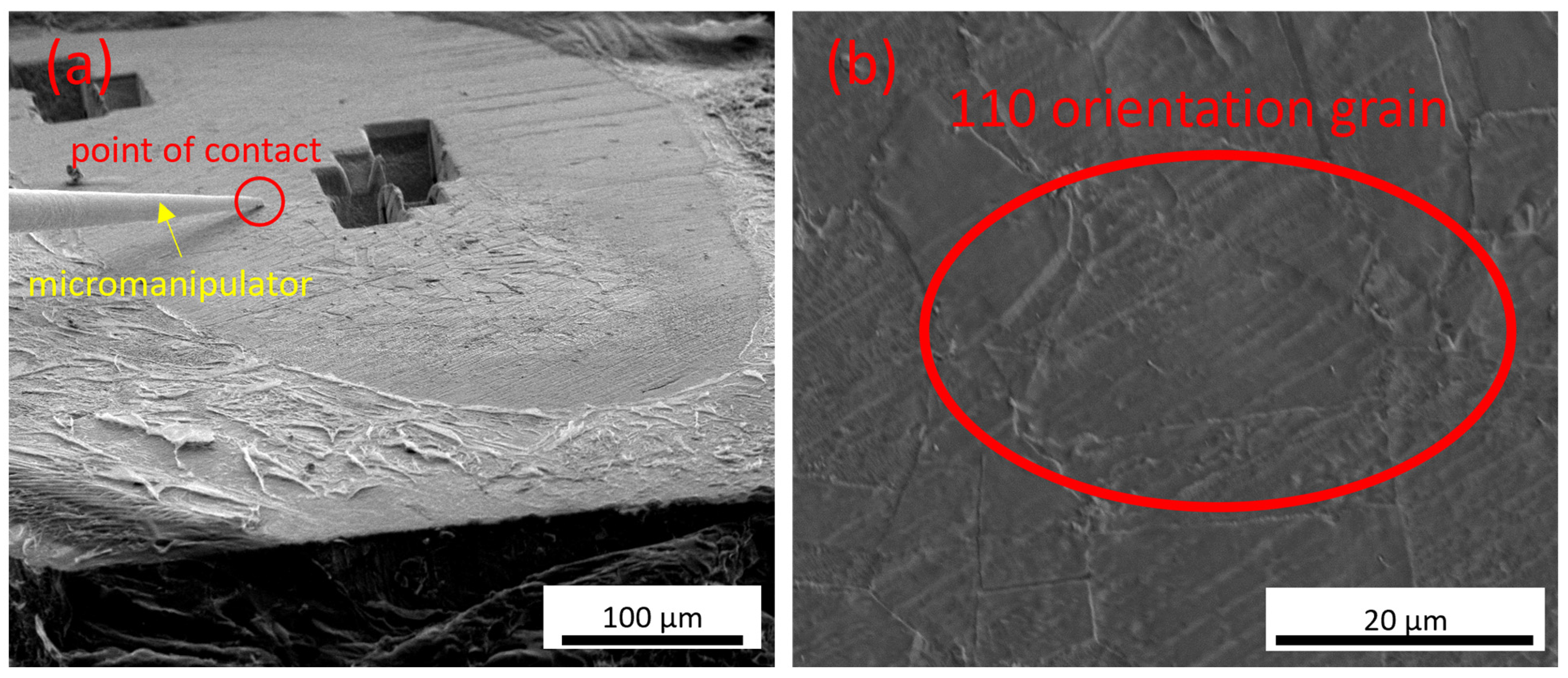
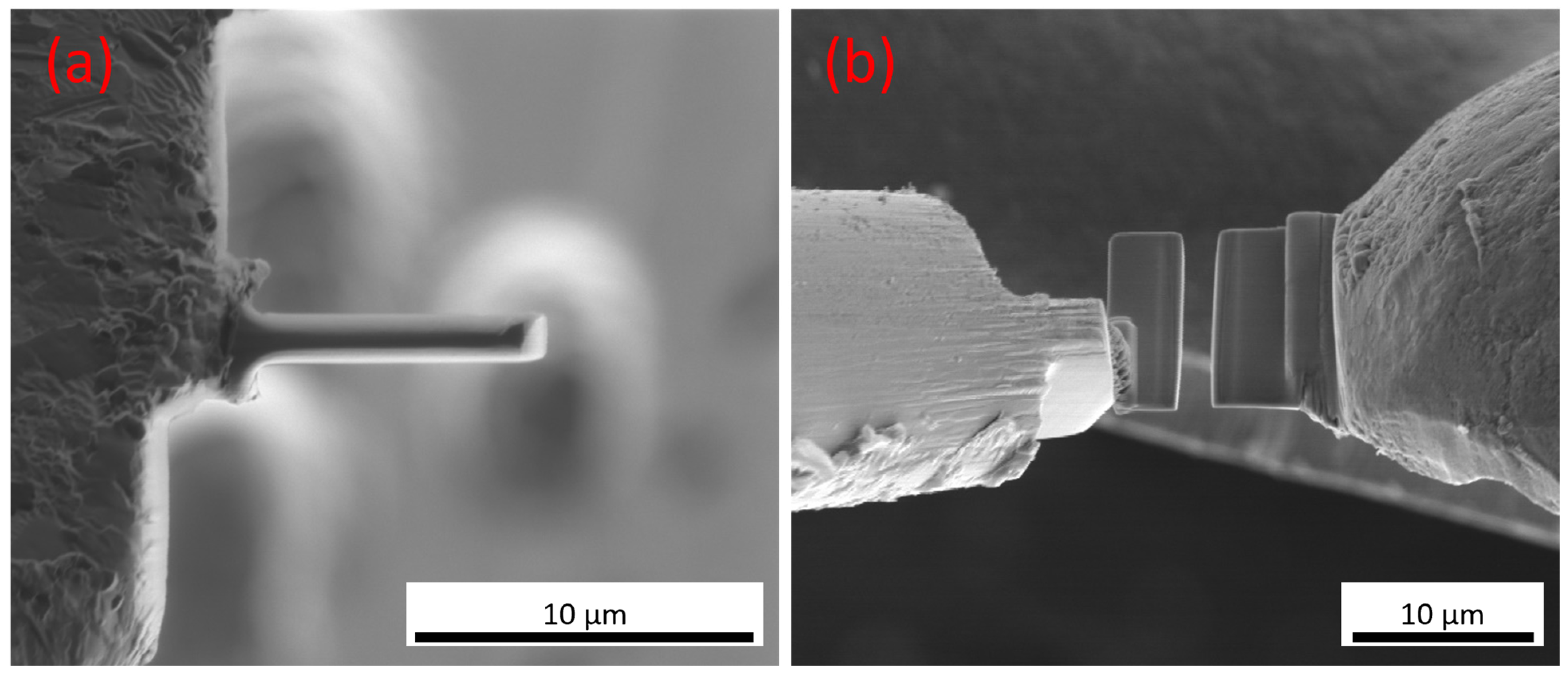
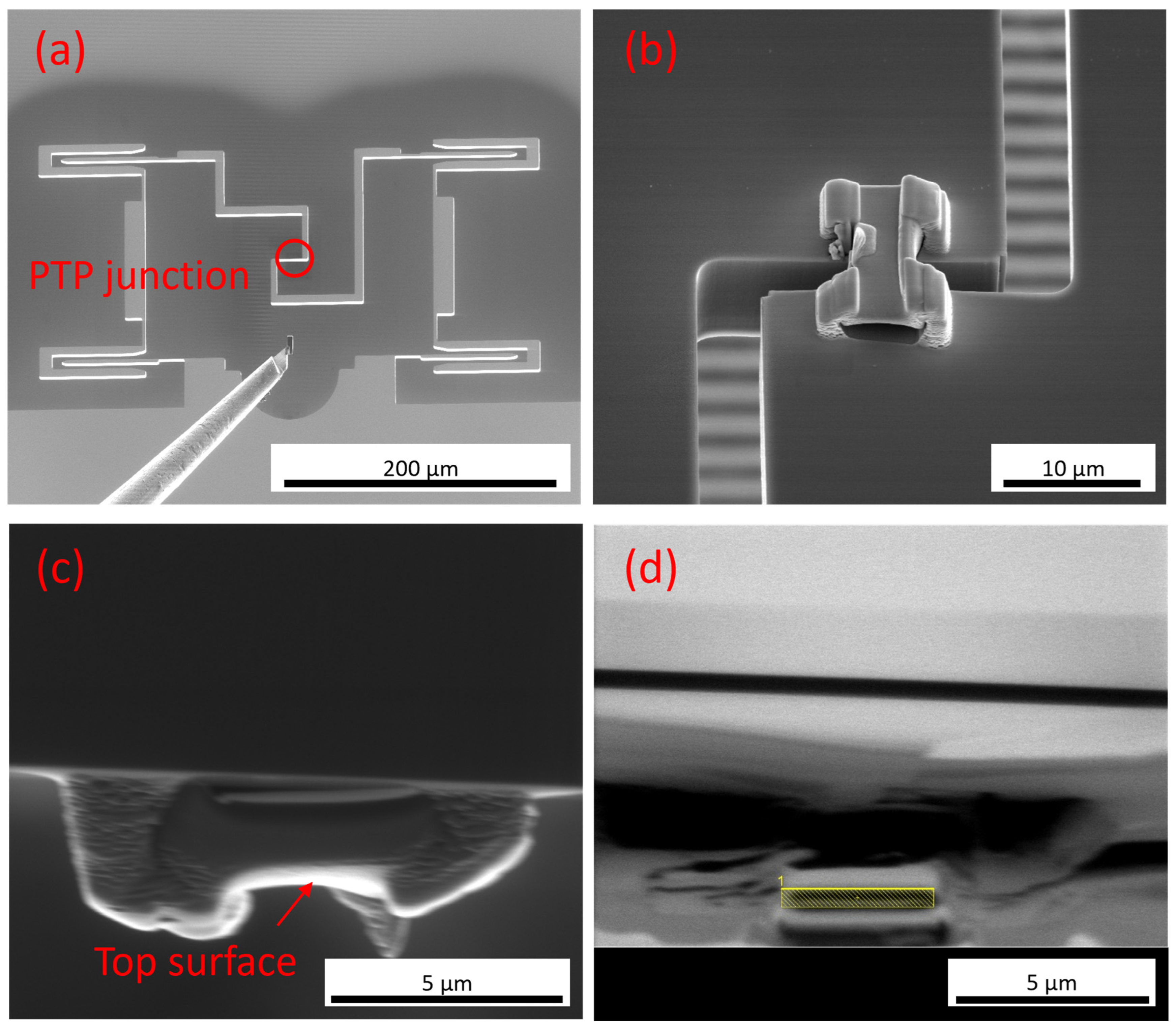
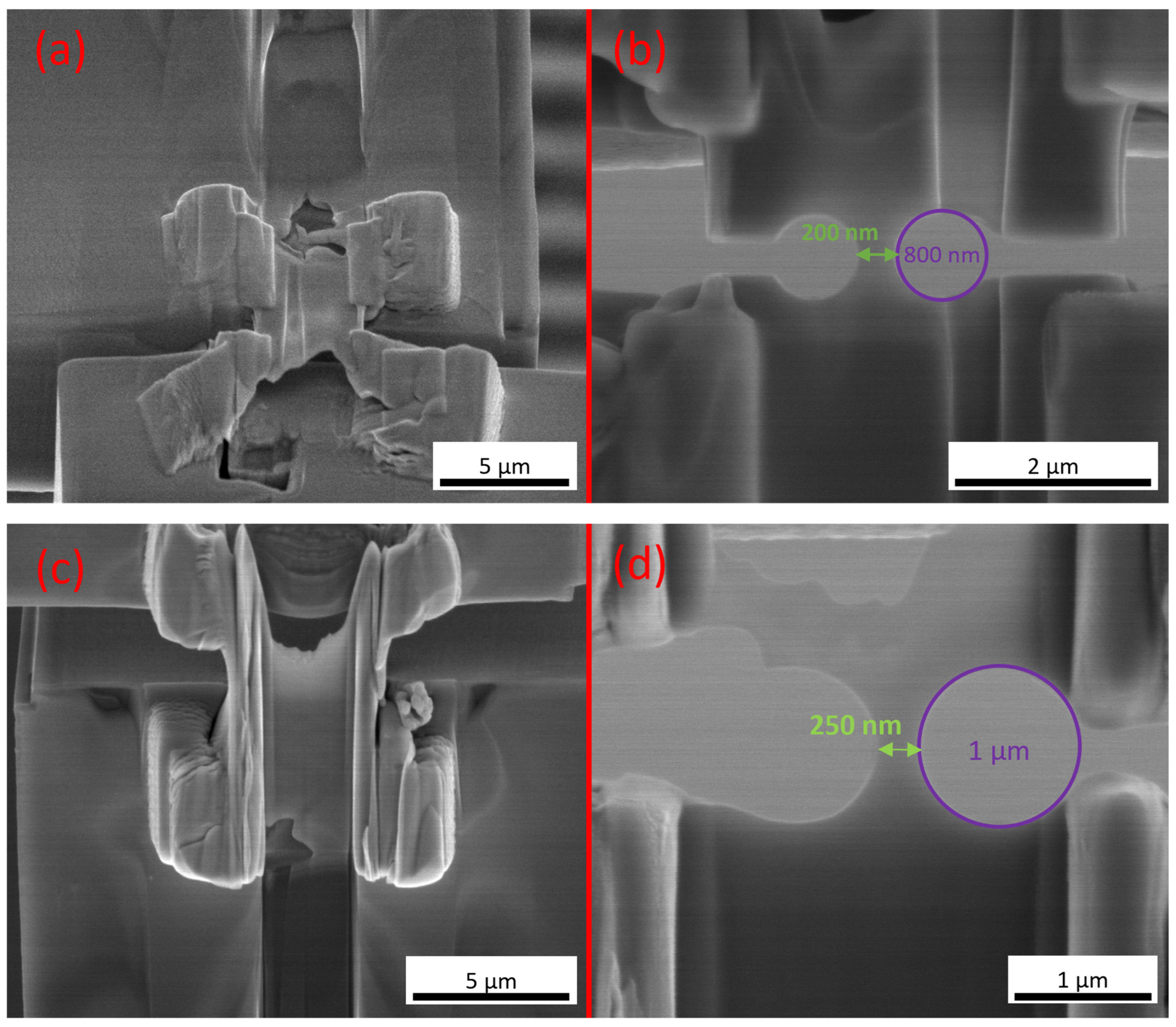
3.1. In-Plane Liftout

The irradiated Inconel X-750 bulk sample was loaded into the FIB chamber on a flat stub using precautionary measures to inflict the lowest radiation dose possible on the user. The chamber was pumped down to < 5 × 10 5 Torr. Due to the significant drift that would not allow for precise deposition or milling while imaging, contact between the micromanipulator and the surface of the material was established to create a conductive path for the sample to discharge, as shown in Figure 2a. An alternative to this measure would be to coat the bulk sample beforehand with carbon or gold. The desired [110] oriented grain was identified in the SEM view (Figure 2b) and after waiting ~5–8 min the imaging drifting became negligible.
A rectangular layer of protective Pt was deposited using the gas injection system (GIS) needle on top of the [110] grain with a low ion beam current (e.g., 0.5–0.1 nA) to prevent inadvertent damage to the surface of the material. The uniform Pt deposition is observed in Figure 3a. A rectangular cross-section pattern allowed for trenching around the sides of the area of interest and a narrow bridge was left on one of the sides as an anchor (Figure 3b). Figure 3c depicts the sample after rotating the stage to be certain that the bottom was milled through before lifting out the sample. Next, the micromanipulator was driven over to the corner of the sample to be welded with Pt and cut free from the support bridge on the opposite corner (Figure 3d).
The in-plane liftout was transferred to a Cu grid. The sample was attached to the side of a post by bringing in the manipulator next to the post and welding it in a flag fashion. Thinning was required to obtain a lamella with a thickness between 0.5 and 1 μm, as shown in Figure 4a. A gradual current decrease from 0.5 nA to 50 pA as the sample became thinner was implemented to avoid FIB-induced damage. The damage discussed in this work includes curtaining and amorphization, which are common fabrication artifacts observed in specimens prepared using the SEM-FIB instrument. Curtaining manifests as vertical streaks or ripples on the milled surface. Amorphization occurs when a crystalline material becomes amorphous due to ion beam irradiation during FIB milling. The high-energy ions used for sputtering disrupt the crystal lattice structure, leading to a loss of long-range atomic order (i.e., amorphization).
The original size of the liftout sample was sufficient to obtain two specimens for testing. Thus, the lamella was divided in half to be attached to the PTP devices (Figure 4b). Each of the PTP devices was loaded into the FIB chamber on 45° pre-tilt holders. In Figure 5a, the circled area in the SEM micrograph of the PTP device denotes the gap in which the lamellas were attached for the nanotensile testing. After securing a lamella on the center junction of the PTP device, Figure 5b was captured at 7° tilt, which is perpendicular to the ion beam at eucentric height. Small rectangular patterns were used to weld the corners, which were monitored continuously to avoid Pt deposition in the center of the sample. Finally, careful thinning of the lamella was performed by tilting gradually ±4° from the normal. Figure 5c depicts the view of the lamella normal to the beam using a low imaging current (e.g., 30 pA) to minimize ion beam damage to the area of interest. Figure 5d shows the placement of the rectangular pattern used for the final thinning of the sample from the top surface, which requires frequent monitoring in both ion and electron window views. Limiting the thinning to be performed only on the top surface prevents the Pt used during welding or the Si from the PTP device from redepositing on the surface of the specimen. Additionally, the last thinning sweeps were completed using 16 kV and currents below 0.1 nA. The last step was polishing the sample with 5 kV at 48 pA to remove any remaining FIB traces.
Figure 6 showcases the two thinned specimens and the gauges readily mounted on the PTP chips for mechanical testing. To prepare the dog-bone-shaped geometries, circular patterns were milled at the center of the areas of interest. The diameters of the circular patterns were defined by a ratio of 1:4 with respect to the gauge widths. For instance, for the first specimen (Figure 6a), the width of the gauge was 200 nm and the diameter of the circular pattern was four times larger (i.e., 800 nm), as indicated in Figure 6a. Similarly, in the second specimen (Figure 6c), the final gauge width measured 250 nm while the diameter of the circular pattern used to mill the dog-bone geometry was set to 1 μm, as showcased in Figure 6d.

3.2. Post-Irradiation Examination and Nanomechanical Testing

The PTP chip with the in-plane liftout specimen was loaded into the Titan TEM for PIE and nanomechanical testing. Initial TEM inspection of the X-750 matrix revealed areas with bubbles and dislocations, which were expected defects due to neutron irradiation. Next, the tensile test was performed using a PI-95 nanoindenter. The experiment was performed at RT with a displacement control set to 1000 nm for 1 min, corresponding to a loading rate of approximately 16.7 nm/s. Figure 7 is a collection of the characterization micrographs post-fracture of the gauge. Figure 7a shows the final state of the specimen after tensile testing; the fracture occurred at the narrowest width in the middle of the gauge. Figure 7b shows a closeup of the fracture site with crack remains and contours accumulated around the strained areas. Defects were spotted on the lower left area of the specimen as shown in insets Figure 7c,d. At a higher magnification, the presence and high density of bubbles are pronounced (indicated by arrows), and some dislocations can be observed scattered across the sample. Figure 7e showcases an indexed FCC [110] selected area electron diffraction (SAED) pattern, thus confirming the successful in-plane retrieval of the desired grain orientation.

4. Discussion

4.1. On the In-Plane Sample Preparation Method

As mentioned in Section 2.2, a grain with a specific orientation was desired for the nanotensile testing due to previous knowledge of the presence and visibility of defects in this orientation. It follows that the in-plane liftout is the most advantageous method to procure this grain. Otherwise, as it is in the case of cross-sectional/transversal liftouts, it is not possible to ensure that the lamella milled out of the bulk sample will only contain a singular oriented grain. As a result, this work offers a pathway for future experiments that can be tailored to study more complex crystal structures (i.e., monoclinic, triclinic, etc.) in cases where mechanical properties are dependent on orientation, which, for example, is the case in highly anisotropic materials.
Finding a grain with enough surface area to retrieve the in-plane liftout may pose a limitation. Yet, procurement of well-polished samples and the use of techniques such as ion etching and EBSD to acquire a clear grain topology map can ease the challenge. Additionally, as shown from our proposed procedure, the ability to produce two specimens from one in-plane liftout is attainable with the selection of a grain with well-defined boundaries and sufficient proportions. This capability will increase the throughput of specimens, reduce the cost of preparing multiple samples, and save instrument time overall.
Special attention was paid to the final steps of sample preparation to guarantee samples viable for the tensile experiments ahead. For instance, once the lamella was mounted on the PTP device, the thinning was performed only on the top surface to prevent resurfacing and redeposition of the Pt used to weld it in place (Figure 5c,d) and avoid milling through the Si material of the PTP chip. For this, the length and the position of the milling pattern must be adjusted accordingly. Moreover, it should be highlighted that using the 1:4 ratio to shape the width of the gauge to the diameter of the milling circle pattern led to the successful fracture of the specimens at the desired necking region.
To minimize artifacts and operate the instrument using best practices, the final cleaning and polishing steps cannot be ignored. Previous studies reported that these steps thwarted the interference of defects caused by the ion beam, deterioration of the samples, and ambiguous data [1,2,25,26]. The visual inspection across the finished specimens before nanomechanical testing in this work did not show parallel vertical lines, which would have been indicative of curtaining or amorphous regions where Ga ions from the beam would have distorted the lattice. Still, reducing the accelerating voltage too low may cause the edges of the gauge to bend, which may be due to the tail of ions being defocused [27,28,29]. The latter was not observed in the samples milled in this paper.
Due to the radioactive nature of the samples, any surfaces the material comes in contact with are considered contaminated. Thus, unlike other procedures [18,27,30] that reuse the grids and/or PTP devices for multiple samples, the proposed procedure is designed to efficiently use the tools once before proper disposal. Additionally, preparing the SEM stage to be loaded with the necessary grids and sample holders at the beginning of the procedure will economize time and possibly require only one reload of the chamber to insert the PTP devices on the pre-tilted mounts for the final thinning and shaping of the specimens. Limiting the number of reloads and pumping and venting the chamber reduces the radiological risk to the personnel involved and prevents unnecessary cleaning and decontamination processes that would be time-consuming and costly. Therefore, the two (or more) specimens from the in-plane liftout must be carefully prepared to ensure proper use of resources.
The preparation of the neutron-irradiated X-750 specimens for PIE and nanomechanical testing via the procedure described in this work can serve as guidelines for sample preparation of other similar radioactive bulk materials. Like other methodologies [27,31,32,33,34] that fabricated specimens for PTP devices, minor tailoring may be needed when choosing accelerating voltages, currents, milling and welding pattern types, and dimensions, depending on the material at hand. Additionally, the outlined steps can also be beneficial for ion-irradiated (non-radioactive) materials. Since the ion penetration depth into the samples is typically shallow (i.e., up to a couple of microns depending on the material, ion species, and its energy) [35], our proposed in-plane liftout procedure would allow the investigation of the ion irradiation-induced effects on the mechanical properties and microstructure on the planar surface.

4.2. On the In Situ Mechanical Testing

EELS was employed to estimate the thickness at the tensile testing area (necking region) of the samples. Equation (1) from Ref. [36] was used to calculate the mean free path of electrons (λ) on the X-750 material:
1 λ = 11 ρ 0.3 200 F E 0 ln α 2 + β 2 + 2 θ E 2 + α 2 β 2 α 2 + β 2 + 2 θ C 2 + α 2 β 2 × θ C 2 θ E 2 ,   F = 1 + E 0 1022 1 + E 0 511 2 ,   θ E = 5.5   ρ 0.3 F E 0 ,   θ C = 20   m r a d ,
where the accelerating voltage ( E 0 ) is 200 kV, the convergence angle (α) is 50 mrad, the collection angle (β) is 150 mrad, and the X-750 alloy density (ρ) is 8.28 g/ c m 3 . The calculated value for λ is estimated to be 109 nm. Consequently, the thickness at the necking area in the specimen ranges between 163 and 190 nm.
Using the data collected from the tensile test, the sample thickness approximation, and the dimensions of the gauge, the stress–displacement curve in Figure 8 was plotted. The stiffness of the PTP device was calculated and subtracted from the original data. The starting linear segment shows the progressive loading applied on the sample up to the discontinuity where the crack propagated until complete fracture. After reaching a displacement of approximately 55 nm, observed as the gap on the stress–displacement curve due to fracture of the specimen, the indenter continued to apply force on the PTP device. Subsequently, the indenter was pulled out, causing the load and resulting stress to gradually decrease until the end of the experiment.
The elastic modulus (E) and ultimate tensile strength (UTS) obtained in this work were estimated to be 48.7 MPa and 2.41 GPa, respectively. The E was calculated by finding the slope of the linear (elastic) region of the graph between 0 and 50 nm of displacement in Figure 8. The UTS was taken to be the highest stress value plotted in the stress–displacement curve. The UTS value was compared to others found in the literature in Table 2 for Ni-based alloys. Sample conditions and experimental setups are also listed for the reader’s consideration. The resulting UTS in this work closely matches the value collected by Wang et al. [37]. Both experiments used a PTP device, yet the difference remains in the use of a nanoindenter in the TEM for this work.
The TEM characterization of the X-750 irradiated material revealed the presence of bubbles and dislocations. These are expected microstructural defects that have been observed in X-750 spacers that have undergone years of radiation exposure in CANDU reactors [43,44]. Particularly, the high density of bubbles was correlated to the downfall of the material as it embrittles due to their agglomeration at the grain boundaries. Furthermore, the present experiments contribute to similar attempts to quantify the micromechanical properties of X-750 using PTP devices for in situ experiments [37,45]. This work highlights the usefulness of coupling EBSD and TEM techniques to analogize the effects of radiation damage to grains with specific orientations, and thus has the potential of facilitating a streamlined process to reduce the complexity of preparing in-plane liftouts, thinning, and mounting the samples for successful experimental testing.

5. Conclusions

In this work, a method for extracting an in-plane liftout and preparing two dog-bone-shaped specimens to be placed in PTP devices for in situ nanomechanical testing and microstructural characterization was developed. Ion etching and EBSD mapping made it possible to identify the desired [110] oriented grain. The steps for fabricating the specimens required the use of low currents for thinning, appropriate milling patterns, and very low current final cleaning and polishing sweeps to output high-quality samples that do not present FIB-related damages such as curtaining or amorphization. Furthermore, in situ tensile testing using a nanoindenter in the TEM was carried out until the complete fracture of the specimen. Examination after the experiment revealed the presence of defects (i.e., high density of bubbles) on the X-750 matrix and confirmed the successful extraction of a [110] grain via SAED pattern indexing.

Author Contributions

Conceptualization, Y.W.; data curation, L.R.G.-H. and T.Y.; formal analysis, L.R.G.-H. and T.Y.; funding acquisition, Y.W.; investigation, L.R.G.-H., T.Y., F.T., M.D.M.II, L.H., and Y.W.; methodology, L.R.G.-H., T.Y. and F.T.; project administration, Y.W.; visualization, L.R.G.-H. and T.Y.; writing—original draft, L.R.G.-H.; writing—review and editing, L.R.G.-H., T.Y., L.H., G.Y. and Y.W. All authors have read and agreed to the published version of the manuscript.

Funding

This work was supported by the U.S. Department of Energy, Office of Nuclear Energy under DOE Idaho Operations Office Contract DE-AC07-051D14517 as part of the Nuclear Science User Facilities. Y. W. acknowledges the support of INL Laboratory Directed Research & Development (LDRD) Program under DOE Idaho Operations Office Contract DE-AC07-05ID14517 (tracking number: 23A1070-069FP). The authors greatly acknowledge all IMCL facility support regarding sample preparation and handling.

Institutional Review Board Statement

This manuscript has been authored by Battelle Energy Alliance, LLC under Contract No. DE-AC07-05ID14517 with the U.S. Department of Energy. The United States Government retains and the publisher, by accepting the article for publication, acknowledges that the United States Government retains a nonexclusive, royalty-free, paid-up, irrevocable, world-wide license to publish or reproduce the published form of this manuscript, or allow others to do so, for United States Government purposes.

Data Availability Statement

The data that support the findings of this study are available from the corresponding author upon reasonable request.

Conflicts of Interest

The authors declare that they have no known competing financial interests or personal relationships that could have appeared to influence the work reported in this paper.

References

  1. Kiener, D.; Motz, C.; Rester, M.; Jenko, M.; Dehm, G. FIB damage of Cu and possible consequences for miniaturized mechanical tests. Mater. Sci. Eng. A 2007, 459, 262–272. [Google Scholar] [CrossRef]
  2. Mayer, J.; Giannuzzi, L.A.; Kamino, T.; Michael, J. TEM Sample Preparation and FIB-Induced Damage. MRS Bull. 2007, 32, 400–407. [Google Scholar] [CrossRef]
  3. Zinkle, S.J.; Busby, J.T. Structural materials for fission & fusion energy. Mater. Today 2009, 12, 12–19. [Google Scholar] [CrossRef]
  4. Dey, G.K. Structural Materials in Nuclear Energy Sector. In Future Landscape of Structural Materials in India; Bhattacharjee, D., Chakrabarti, S., Eds.; Springer Nature: Singapore, 2022; pp. 59–77. [Google Scholar]
  5. Murty, K.L.; Charit, I. Structural materials for Gen-IV nuclear reactors: Challenges and opportunities. J. Nucl. Mater. 2008, 383, 189–195. [Google Scholar] [CrossRef]
  6. Zinkle, S.J.; Was, G.S. Materials challenges in nuclear energy. Acta Mater. 2013, 61, 735–758. [Google Scholar] [CrossRef]
  7. Judge, C.D.; Griffiths, M.; Walters, L.; Wright, M.; Bickel, G.A.; Woo, O.T.; Stewart, M.; Douglas, S.R.; Garner, F.A. Embrittlement of Nickel Alloys in a CANDU Reactor Environment. In Effects of Radiation on Nuclear Materials: 25th Volume; Yamamoto, T., Ed.; ASTM International: West Conshohocken, PA, USA, 2013; pp. 161–175. [Google Scholar]
  8. Bruemmer, S.M.; Simonen, E.P.; Scott, P.M.; Andresen, P.L.; Was, G.S.; Nelson, J.L. Radiation-induced material changes and susceptibility to intergranular failure of light-water-reactor core internals. J. Nucl. Mater. 1999, 274, 299–314. [Google Scholar] [CrossRef]
  9. Griffiths, M. Ni-Based Alloys for Reactor Internals and Steam Generator Applications. In Structural Alloys for Nuclear Energy Applications; Elsevier: Amsterdam, The Netherlands, 2019; pp. 349–409. [Google Scholar]
  10. Zhang, H.K.; Yao, Z.; Kirk, M.A.; Daymond, M.R. Stability of Ni3(Al, Ti) Gamma Prime Precipitates in a Nickel-Based Superalloy Inconel X-750 Under Heavy Ion Irradiation. Metall. Mater. Trans. A 2014, 45, 3422–3428. [Google Scholar] [CrossRef]
  11. Changizian, P.; Brooks, A.; Yao, Z.; Daymond, M.R. Nano-scale Mechanical Properties and Microstructure of Irradiated X-750 Ni-Based Superalloy. Metall. Mater. Trans. A 2018, 49, 498–514. [Google Scholar] [CrossRef]
  12. Mills, W.J. The deformation and fracture characteristics of inconel X-750 at room temperature and elevated temperatures. Metall. Trans. A 1980, 11, 1039–1047. [Google Scholar] [CrossRef]
  13. Gabrielli, F.; Pelloux, R.M. Effect of Environment on Fatigue and Creep Crack Growth in Inconel X-750 at Elevated Temperature. Metall. Trans. A 1982, 13, 1083–1090. [Google Scholar] [CrossRef]
  14. Venkiteswaran, P.K.; Taplin, D.M.R. The Creep Fracture of Inconel X-750 at 700 °C. Met. Sci. 1974, 8, 97–106. [Google Scholar] [CrossRef]
  15. Kacher, J.; Kirchlechner, C.; Michler, J.; Polatidis, E.; Schwaiger, R.; Van Swygenhoven, H.; Taheri, M.; Legros, M. Impact of in situ nanomechanics on physical metallurgy. MRS Bull. 2019, 44, 465–470. [Google Scholar] [CrossRef]
  16. Greer, J.R.; Kim, J.-Y.; Burek, M.J. The in-situ mechanical testing of nanoscale single-crystalline nanopillars. JOM 2009, 61, 19–25. [Google Scholar] [CrossRef]
  17. Yu, Q.; Legros, M.; Minor, A.M. In situ TEM nanomechanics. MRS Bull. 2015, 40, 62–70. [Google Scholar] [CrossRef]
  18. Kobler, A.; Brandl, C.; Hahn, H.; Kübel, C. In situ observation of deformation processes in nanocrystalline face-centered cubic metals. Beilstein J. Nanotechnol. 2016, 7, 572–580. [Google Scholar] [CrossRef] [PubMed]
  19. Kobler, A.; Kashiwar, A.; Hahn, H.; Kübel, C. Combination of in situ straining and ACOM TEM: A novel method for analysis of plastic deformation of nanocrystalline metals. Ultramicroscopy 2013, 128, 68–81. [Google Scholar] [CrossRef]
  20. Kiener, D.; Motz, C.; Dehm, G.; Pippan, R. Overview on established and novel FIB based miniaturized mechanical testing using in-situ SEM. Int. J. Mater. Res. 2009, 100, 1074–1087. [Google Scholar] [CrossRef]
  21. Legros, M.; Gianola, D.S.; Motz, C. Quantitative In Situ Mechanical Testing in Electron Microscopes. MRS Bull. 2010, 35, 354–360. [Google Scholar] [CrossRef]
  22. Griffiths, M.; Walters, L.; Greenwood, L.; Garner, F. Accelerated materials evaluation for nuclear applications. J. Nucl. Mater. 2017, 488, 46–62. [Google Scholar] [CrossRef]
  23. Greenwood, L.R.; Smither, R.K. SPECTER: Neutron Damage Calculations for Materials Irradiations; ANL/FPP/TM-197; Argonne National Laboratory: Argonne, IL, USA, 1985. [Google Scholar]
  24. Howard, C.; Judge, C.; Poff, D.; Parker, S.; Griffiths, M.; Hosemann, P. A novel in-situ, lift-out, three-point bend technique to quantify the mechanical properties of an ex-service neutron irradiated inconel X-750 component. J. Nucl. Mater. 2018, 498, 149–158. [Google Scholar] [CrossRef]
  25. Aitkaliyeva, A.; Madden, J.; Miller, B.; Hyde, T. Radioactive Sample Preparation using Focused Ion Beam. Microsc. Microanal. 2013, 19, 904–905. [Google Scholar] [CrossRef]
  26. Wirth, R. Focused Ion Beam (FIB) combined with SEM and TEM: Advanced analytical tools for studies of chemical composition, microstructure and crystal structure in geomaterials on a nanometre scale. Chem. Geol. 2009, 261, 217–229. [Google Scholar] [CrossRef]
  27. Bikmukhametov, I.; Koenig, T.R.; Tucker, G.J.; Thompson, G.B. A rapid preparation method for in situ nanomechanical TEM tensile specimens. J. Mater. Res. 2021, 36, 2315–2324. [Google Scholar] [CrossRef]
  28. Tang, L.J.; Zhang, Y.J.; Bosman, M.; Jasmine, W. Study of ion beam damage on FIB prepared TEM samples. In Proceedings of the 2010 17th IEEE International Symposium on the Physical and Failure Analysis of Integrated Circuits (IPFA 2010), Singapore, 5–9 July 2010; pp. 1–4. [Google Scholar]
  29. Drezner, Y.; Greenzweig, Y.; Tan, S.; Livengood, R.H.; Raveh, A. High resolution TEM analysis of focused ion beam amorphized regions in single crystal silicon—A complementary materials analysis of the teardrop method. J. Vac. Sci. Technol. B Nanotechnol. Microelectron. Mater. Process. Meas. Pheno 2017, 35, 011801. [Google Scholar] [CrossRef]
  30. Bufford, D.C.; Stauffer, D.; Mook, W.M.; Syed Asif, S.A.; Boyce, B.L.; Hattar, K. High Cycle Fatigue in the Transmission Electron Microscope. Nano Lett. 2016, 16, 4946–4953. [Google Scholar] [CrossRef]
  31. Gammer, C.; Kacher, J.; Czarnik, C.; Warren, O.L.; Ciston, J.; Minor, A.M. Local and transient nanoscale strain mapping during in situ deformation. Appl. Phys. Lett. 2016, 109, 081906. [Google Scholar] [CrossRef]
  32. Samaeeaghmiyoni, V.; Idrissi, H.; Groten, J.; Schwaiger, R.; Schryvers, D. Quantitative in-situ TEM nanotensile testing of single crystal Ni facilitated by a new sample preparation approach. Micron 2017, 94, 66–73. [Google Scholar] [CrossRef] [PubMed]
  33. Warren, P.H.; Warren, G.; Dubey, M.; Burns, J.; Wu, Y.Q.; Wharry, J.P. Method for Fabricating Depth-Specific TEM In Situ Tensile Bars. JOM 2020, 72, 2057–2064. [Google Scholar] [CrossRef]
  34. Idrissi, H.; Samaee, V.; Lumbeeck, G.; Van Der Werf, T.; Pardoen, T.; Schryvers, D.; Cordier, P. In Situ Quantitative Tensile Testing of Antigorite in a Transmission Electron Microscope. JGR Solid Earth 2020, 125, e2019JB018383. [Google Scholar] [CrossRef]
  35. Changizian, P.; Lu, C.; Yao, Z.; Wang, L. Indentation behaviour of ion-irradiated X-750 Ni-based superalloy. Philos. Mag. Lett. 2017, 97, 101–109. [Google Scholar] [CrossRef]
  36. Iakoubovskii, K.; Mitsuishi, K.; Nakayama, Y.; Furuya, K. Thickness measurements with electron energy loss spectroscopy. Microsc. Res Tech. 2008, 71, 626–631. [Google Scholar] [CrossRef] [PubMed]
  37. Wang, Y.; Liu, X.; Murray, D.J.; Teng, F.; Jiang, W.; Bachhav, M.; Hawkins, L.; Perez, E.; Sun, C.; Bai, X.; et al. Measurement of grain boundary strength of Inconel X-750 superalloy using in-situ micro-tensile testing techniques in FIB/SEM system. Mater. Sci. Eng. A 2022, 849, 143475. [Google Scholar] [CrossRef]
  38. Howard, C.; Bhakhri, V.; Dixon, C.; Rajakumar, H.; Mayhew, C.; Judge, C.D. Coupling multi-scale mechanical testing techniques reveals the existence of a trans-granular channel fracture deformation mechanism in high dose Inconel X-750. J. Nucl. Mater. 2019, 517, 17–34. [Google Scholar] [CrossRef]
  39. Wang, K.; Du, D.; Liu, G.; Pu, Z.; Chang, B.; Ju, J. Microstructure and mechanical properties of high chromium nickel-based superalloy fabricated by laser metal deposition. Mater. Sci. Eng. A 2020, 780, 139185. [Google Scholar] [CrossRef]
  40. Slone, C.E.; Miao, J.; Mills, M.J. Ultra-high strength and ductility from rolling and annealing of a Ni-Cr-Co superalloy. Scr. Mater. 2018, 155, 94–98. [Google Scholar] [CrossRef]
  41. Petley, V.; Sathishkumar, S.; Thulasi Raman, K.H.; Rao, G.M.; Chandrasekhar, U. Microstructural and mechanical characteristics of Ni–Cr thin films. Mater. Res. Bull. 2015, 66, 59–64. [Google Scholar] [CrossRef]
  42. Bauer, J.; Costa, J.F.; Carvalho, C.N.; Grande, R.H.M.; Loguercio, A.D.; Reis, A. Characterization of two Ni–Cr dental alloys and the influence of casting mode on mechanical properties. J. Prosthodont. Res. 2012, 56, 264–271. [Google Scholar] [CrossRef]
  43. Zhang, H.K.; Yao, Z.; Morin, G.; Griffiths, M. TEM characterization of in-reactor neutron irradiated CANDU spacer material Inconel X-750. J. Nucl. Mater. 2014, 451, 88–96. [Google Scholar] [CrossRef]
  44. Judge, C.D.; Gauquelin, N.; Walters, L.; Wright, M.; Cole, J.I.; Madden, J.; Botton, G.A.; Griffiths, M. Intergranular fracture in irradiated Inconel X-750 containing very high concentrations of helium and hydrogen. J. Nucl. Mater. 2015, 457, 165–172. [Google Scholar] [CrossRef]
  45. Howard, C.; Judge, C.D.; Hosemann, P. Applying a new push-to-pull micro-tensile testing technique to evaluate the mechanical properties of high dose Inconel X-750. Mater. Sci. Eng. A 2019, 748, 396–406. [Google Scholar] [CrossRef]
Figure 1. Grain topology (a) after ion etching of the irradiated X-750 material where the [110] oriented grain is encircled and correlated to (b) the EBSD color-coded map.
Energies 17 04199 g001
Figure 2. SEM micrographs at the surface of the sample show; (a) the use of the micromanipulator to prevent drifting and (b) the [110] oriented grain chosen for the liftout.
Energies 17 04199 g002
Figure 3. Steps before de-attachment of the in-plane liftout from the bulk material: (a) deposition of Pt protective layer, (b) milled areas around the sides of the sample, (c) check that the sample is cut through underneath, and (d) attachment to the micromanipulator for liftout.
Energies 17 04199 g003
Figure 4. Micrographs of (a) the thinned lamella attached in a flag style to a Cu grid post and (b) the separation of the first specimen using the micromanipulator to be transferred to the PTP device.
Energies 17 04199 g004
Figure 5. Micrograph of (a) the view of the micromanipulator holding one lamella and the encircled area on the PTP device to be placed. (b) Attached lamella using four rectangular patterns on the corners to prevent redeposition. (c,d) Imaging the samples at different currents showing the top surface and the rectangular pattern for the final thinning and polishing steps.
Energies 17 04199 g005
Figure 6. Finished samples for nanomechanical testing showing dog-bone geometries with diameter-to-circular pattern ratio of 1:4 such that (a,b) the first specimen has a gauge width of 200 nm and the circular pattern for milling was 800 nm and (c,d) the second specimen has a gauge width of 250 nm and the circular pattern for milling was 1 µm.
Energies 17 04199 g006
Figure 7. PIE micrographs of (a) the specimen after fracture, (b) a zoomed-in view at the fracture site, (c) the bottom left corner of the sample with (d) bubbles and dislocations from inset (c) at a higher magnification, and (e) an indexed FCC [110] SAED pattern. Blue (b) and orange (c) insets are high-magnification micrographs of (a). Yellow (d) and green (e) insets are high-magnification micrograph and diffraction pattern of (c), respectively. For interpretation of the colors in the figure, the reader is referred to the web version of this article.
Energies 17 04199 g007
Figure 8. Stress–displacement curve of the X-750 specimen tensile testing.
Energies 17 04199 g008
Table 1. Chemical composition of Inconel X-750 [24].
ElementAlCCoCrCuFeMnNiSSiTiNb + Ta
Concentration (wt %)0.4–10.08114–170.55–91700.010.52.25–2.750.7–1.2
Solution Treatment1093–1204 °C
Precipitation Hardening732 ± 14 ℃ for 16.5 hrs., air cool
Table 2. Comparison of UTS values of Ni-based alloys.
ReferenceMaterialSample ConditionSystemUTS (GPa)
This workInconel X-750Irradiated (67 dpa)PTP–TEM2.41
Ref. [37]Inconel X-750Non-irradiatedCantilever–SEM1.4
Irradiated (1.5 dpa)1.3
Non-irradiatedPTP–SEM2.05
Irradiated (1.5 dpa)2.20
Ref. [38]Inconel X-750Non-irradiatedPTP–SEM0.956
Irradiated (84 dpa)1.817
Ref. [39]K648Additively manufacturedIndentation–SEM0.83
Ref. [40]Inconel 740HRolled and annealedElectro-thermal Mechanical Tester1.099
Ref. [41]Ni-CrThin filmNanoindentation1.05
Ref. [42]Ni-CrCastingMechanical Tester1.057
Disclaimer/Publisher’s Note: The statements, opinions and data contained in all publications are solely those of the individual author(s) and contributor(s) and not of MDPI and/or the editor(s). MDPI and/or the editor(s) disclaim responsibility for any injury to people or property resulting from any ideas, methods, instructions or products referred to in the content.

