1. Introduction
With the wide application of nonlinear loads represented by power electronic devices, a large number of harmonics has been injected into the power grid in recent decades [
1]. Active power filter [
2] (APF), due to its capability to suppress effectively harmonics and improve the system power factor [
3], has been widely applied in various fields such as high-voltage direct current transmission [
4], motor drives [
5], as well as grid-connected photovoltaic [
6] and wind power [
7].
For the APF with a voltage inverter structure, DC voltage is one of the important parameters to ensure its stability and harmonic suppression effect. The voltage-type inverter can be regarded as a proportional amplification block [
8] when using sinusoidal pulse width modulation (PWM) technology, and when the carrier frequency is high enough. However, the amplification factor, which is mainly determined by the DC voltage, is an important parameter that affects the filtering effect of APF. Therefore, DC voltage should neither be too high nor too low. If the DC voltage is too high while the system current is too low, the inverter output current waveform will become “coarse”, containing large switching frequency harmonic content, thereby reducing the harmonic suppression effect. In contrast, if the DC voltage is too low while the system current is too high, disturbed input voltage will cause more distortion of the output current, also reducing the harmonic suppression effect. The unchanged DC voltage cannot adapt to different working conditions automatically. Consequently, the DC voltage of the APF should be matched with the magnitude of the system current and should preferably be automatically adjusted according to the changes in operating conditions.
Since the series APF is an in series connection in the system, the switching devices such as IGBT do not need to withstand the large fundamental voltages of the power grid. Therefore, series APF has more advantages in 10 kV or 35 kV distribution network harmonic suppression. However, the series APF also has a disadvantage that its DC voltage is too difficult to be controlled automatically. The essence of DC voltage control is energy exchange between the APF and the power grid. According to circuit theory, this energy exchange should meet the following two basic conditions:
- (1)
The APF must withstand a certain amount of fundamental voltage
- (2)
The inverter of APF must generate a same-phase current component with the above fundamental voltage.
Since the voltage and current are in the same phase, the APF can absorb energy from the power grid [
9,
10] and store it in the DC link energy storage capacitor, causing the DC voltage to increase.
DC voltage control for series APF and shunt APF is completely different. The shunt APF is connected in parallel with the power grid and withstands the total fundamental voltage of the power grid. This fundamental voltage is basically equal to the rated voltage of the power grid and is large enough. It is also very easy to detect and phase-lock. The above two conditions are easily satisfied. Hence recent research on DC voltage control of APF was almost entirely based on shunt APF [
11,
12,
13]. In contrast, series APF is completely different. Both of the aforementioned conditions are extremely difficult to satisfy. Due to being connected in series within the power grid, series APF withstands nearly no fundamental voltage. In addition, series APF withstands significant harmonic voltages during normal working conditions. Even though some artificial special settings can create some fundamental voltage on the series APF, this fundamental voltage would be mixed with large harmonic voltages. It is very difficult to detect accurately the fundamental voltage and lock its phase. The phase of the inverter output current component cannot be determined. Therefore, the aforementioned condition 2 cannot be satisfied either. For these reasons, the DC voltage of series APF has been theoretically uncontrollable until now, and there have been few studies on DC voltage control for series APF. Series APF of all types needs an extra DC source such as rectifier equipment, to charge its DC bus when it is working.
Up to now, in the series APF DC voltage control technology field, only reference [
14] has proposed an experimental approach for DC voltage control of series hybrid APF (SHAPF) with magnetic flux compensation (MFC). The principle of magnetic flux compensation was first proposed by Dayi Li, Qiaofu Chen, and others [
15]. It has been applied in many fields, including series hybrid APF [
15,
16], shunt APF [
17], controllable reactors [
18], and arc-suppression coils [
19], all of which have achieved good results. A high power SHAPF with MFC can be realized by using a transformer structure that contains one primary winding and multiple secondary windings [
16]. Moreover, this type of SHAPF has already been applied in engineering, and its filtering performance is quite excellent [
20]. For the DC voltage control of SHAPF with MFC, the basic idea in reference [
14] is setting the fundamental flux compensation coefficient
α less than 1, so that the series transformer (ST) of the SHAPF will withstand a certain amount of fundamental voltage, satisfying condition 1. Then an evasive attitude is adopted for condition 2. The phase of this fundamental voltage component is simply assumed to lead the phase of the primary winding current by 90°. The inverter generates an unchanged current component for DC voltage control, which is denoted as
I2p. The amplitude of
I2p is very small, and the phase of
I2p leads the fundamental component of the system current
I1(1) by 90°. So
I2p will be in the same phase with the above fundamental voltage component after transformer winding conversion. Thus, the inverter will absorb power from the power grid. When the absorbed power is greater than the SHAPF power loss, the DC voltage will increase. On the other hand, if
I2p is equal to 0, SHAPF cannot absorb power from the power grid. The DC voltage will be declined by the power loss of SHAPF itself.
Although this method realizes SHAPF DC voltage control initially, there are still several shortcomings which are difficult to solve. The fundamental magnetic flux compensation coefficient
α is not equal to 1; that means the fundamental magnetic flux compensation condition is not satisfied, and the filtering effects will be reduced. A much more serious problem is that the DC voltage control current component
I2p will affect the fundamental voltage on ST. The phase of the fundamental voltage component on ST will not lead the phase of the primary winding current of ST by 90° when
I2p is not equal to 0. This means that the theoretical premise of the method in reference [
14] is not rigorous. And the relationship between the
I2p and the SHAPF to absorb power from the power grid is quite complex. It is even possible that increasing
I2p may lead to a decrease in the power absorbed by SHAPF from the power grid. If a faster dynamic process is required, this method cannot even determine whether the control coefficient should be increased or decreased. Selecting appropriate control parameters for this method is very difficult. These aforementioned limitations restrict the application of this method. Apart from the publication of this paper, no further research in DC voltage control technology for series APF has been seen over the past decade.
Based on the work in reference [
14], an improved DC voltage control method for SHAPF with MFC is proposed in this paper. First, the fundamental magnetic flux compensation coefficient
α is set to 1. Then, a DC voltage control component, also denoted as
I2p, is added to the output current of the inverter. The phase of
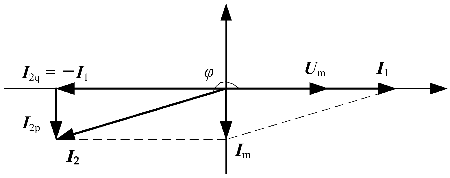
I2p lags the phase of the fundamental component of the primary winding current by 90°. Since
α is equal to 1,
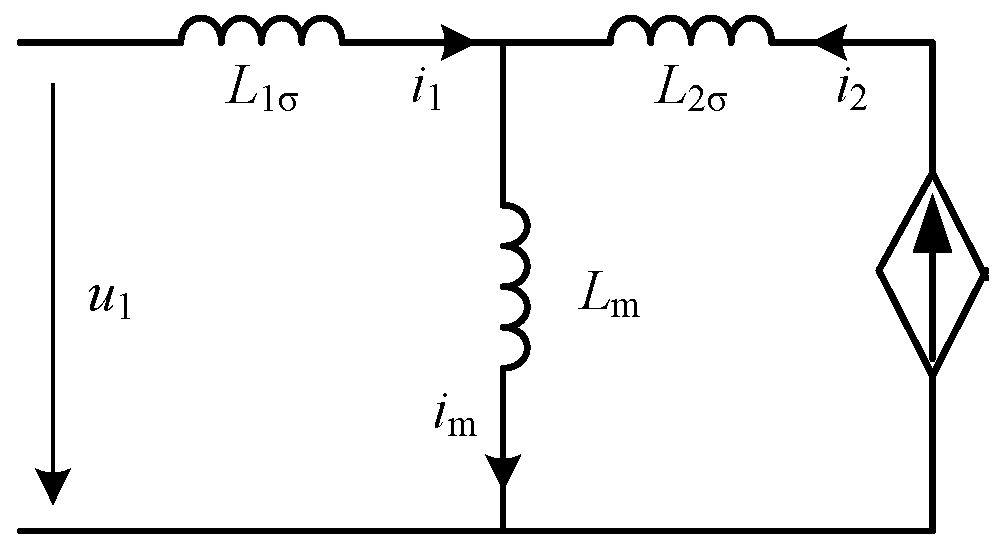
I2p will flow through the magnetizing branch of ST and produce a fundamental voltage on the magnetizing inductance. This fundamental voltage is in the same phase as the fundamental wave component of the primary winding current. The fundamental voltage and current are in the same phase so that the inverter can absorb energy from the power grid. And the DC voltage will be well controlled if this energy is appropriate.
The improved method proposed in this paper ensures that the phase of the fundamental voltage on primary winding of ST is independent of the magnitude
I2p. The power absorbed by the inverter from the power grid is linearly related to
I2p, completely solving the problems and shortcomings of the previous method proposed in reference [
14]. The design difficulty of the control parameters is significantly reduced.
3. Validation of Simulation
In recent years, a large amount of research on SHAPF with FMC has been published. The correctness of the working principle, the control performance of the inverter, and the effectiveness in harmonic suppression have been verified by a large number of simulations and experiments. On that account, this paper focuses on the correctness and feasibility of the improved DC voltage control method, but focuses less on the filtering performance of SHAPF with MFC.
SHAPF with MFC was applied in a 10 kV and 1 MVA factory in Guangdong province [
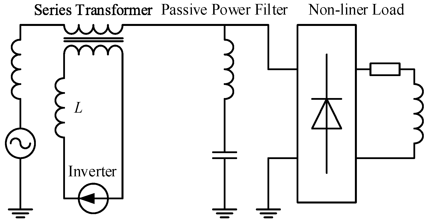
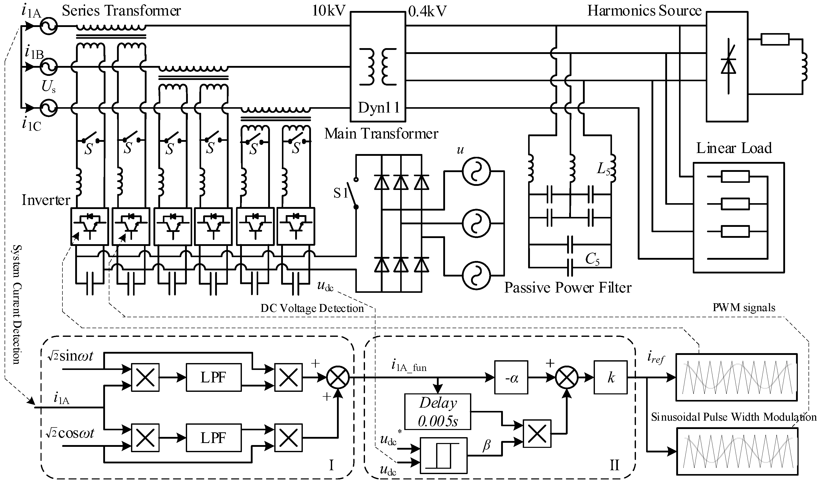
20], and the experiment validation in the next section was carried out on this prototype. In order to make the simulation results more convincing, this section establishes the simulation circuit as shown in
Figure 5 based on the actual SHAPF prototype [
23]. The system voltage
Us = 10 kV, the rated parameters of the main transformer are 1 MVA, 10/0.4 kV. The harmonic source is a three-phase thyristor phase-controlled rectifier bridge, and the series resistive and inductive load parameters after rectification are 0.2 Ω and 4 mH. Other actual linear loads such as electric furnaces, motors, production lines, and industrial fans are replaced by three-phase 0.5 Ω linear resistors in the simulation circuit. PPF is a 5th-order single-tuned filter branch in parallel connection at the 400 V side. Its parameters are
L5 = 146 μH,
C5 = 693 μF. The three-phase capacitors are connected in Δ configuration. Since the dynamic performance of PPF is not of concern in this paper, the switch of the PPF was removed from the simulation circuit, so that the PPF is always in the working state.
The active part of SHAPF adopts three single-phase structures and is connected in series at the high-voltage 10 kV side. The ST adopts a dual secondary winding configuration [
16], with a turn ratio of 10:1:1. Therefore there are six single-phase H-bridge inverters in the SHAPF, and the output inductance of each inverter is 1 mH. DC energy storage capacitors of all inverters are connected together. An independent three-phase power supply charges the DC storage capacitor of the inverter through a diode-uncontrolled rectifier bridge. This independent three-phase power supply is denoted as
u and equal to 80 V during the simulation process.
The APF switch is denoted as S. At the beginning of simulation, S is closed, which means that the secondary winding of ST is in the short-circuit state and the output load of the inverter only contains the output inductance L. Then S disconnects at t = 0.06 s; here t is the simulation time. Then the output current of the inverter is injected into the secondary winding of ST, and the APF is put into operation. S1 is the connection switch between the uncontrolled rectifier bridge and the DC bus. It is closed initially and disconnects at t = 0.2 s. Then the DC voltage is controlled by the improved method proposed in this paper.
The control block diagram of SHAPF is shown in the lower part of
Figure 5. Since SHAPF adopts three independent single-phase structures, the control system is also independent. The control block diagram of each phase is exactly the same, therefore only the A-phase control block diagram is given in
Figure 5. The control block Ι is the fundamental current detection block, which is used to obtain the fundamental component
i1A_fun in the A-phase system current
i1. Single phase fundamental current detection adopts the method described in reference [
24]. The basic idea is to multiply the current signal
i1A with the power frequency sinusoidal signal. If the sinusoidal signal is in same phase as the power grid voltage, a virtual fundamental active current can be obtained after the product passes through a low pass filter (LPF). Similarly, by multiplying
i1A with a cosine signal that is in same phase with the power grid voltage and passing through an LPF, a virtual fundamental reactive current can be also obtained. These two virtual currents are multiplied by the sine and cosine signals. respectively, and then added together. The result is the fundamental current component
i1A_fun in
i1A. If only
i1A_fun is required, without the need for the actual fundamental active current and fundamental reactive current, then the phase of the sine and cosine signals does not need to be consistent with the phase of the voltage of the power grid. The phase-locked loop is no longer needed in this case. Sinusoidal and cosine signals can be given directly in the control system.
The control block II is the reference current generation block. Since i1A_fun was obtained in control block I, delaying it by one quarter of the fundamental period (equivalent to a phase lag of 90°), and then multiplying it by the control coefficient β gives the active current command i2p as shown in Equation (7). The control coefficient β is obtained based on the relationship between the target value udc* and the actual value udc of the DC voltage. The specific process is described in detail in the next paragraph.
Simultaneously, multiplying i1A_fun by the fundamental flux compensation coefficient α (α = 1 in simulation), then adding the result to i2p gives the inverter output instruction. Due to the series transformer with a double winding and a turn ratio of 10:1:1, the instruction needs to be multiplied by a coefficient k = 5, to obtain the final current output reference signal iref for the two A-phase inverters. Then the PMW driving signal is generated by the sinusoidal pulse width modulation circuit, and the two A-phase inverters of SHAPF are driven.
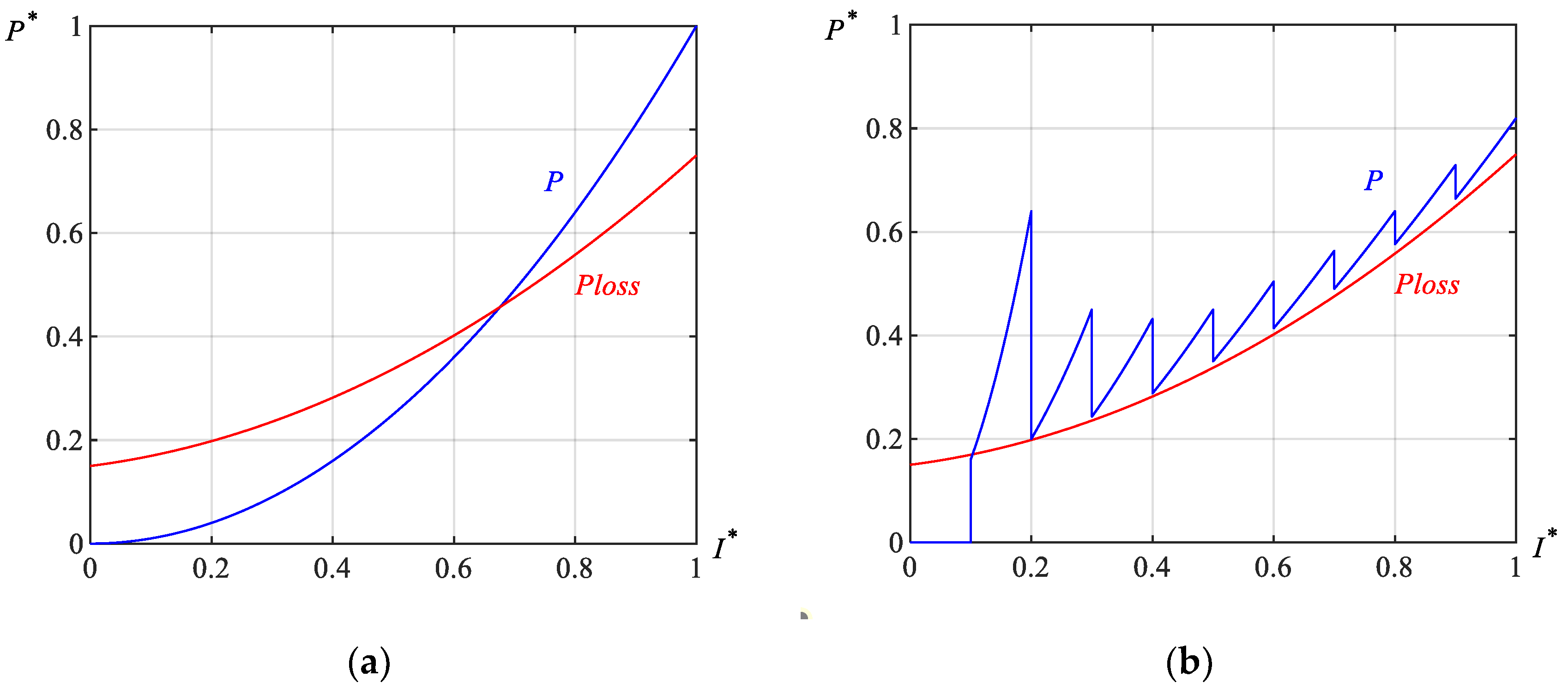
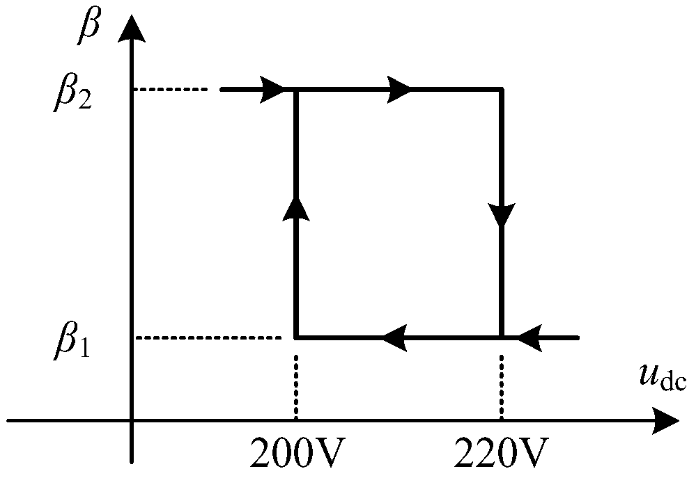
In order to observe the DC voltage control effect in detail, the double threshold voltage command 200 V and 220 V was adopted in controller block II, as shown in
Figure 6. It is quite similar to the hysteresis control strategy [
25]. When the actual value of the DC voltage
udc is too high and needs to decline, a smaller value
β1 is set in the control algorithm. The power absorbed by SHAPF from power grid
P is less than the total power loss
Ploss, therefore
udc declines. On the contrary, when
udc drops to 200 V and needs to increase again, a larger value
β2 is set in the control algorithm.
P is larger than
Ploss. As a result,
udc increases. And when
udc increases to 220 V again, setting the smaller value of
β1 declines
udc. The above process, when repeated cyclically, can control the DC voltage of SHAPF between 200 V and 220 V.
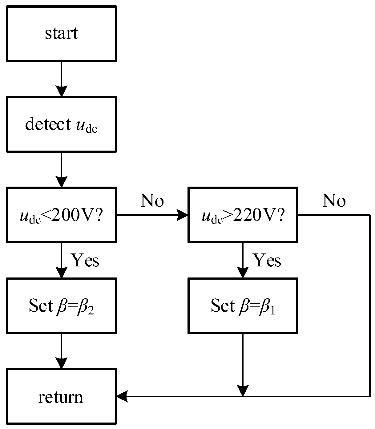
A simple control algorithm diagram is shown as
Figure 7. The first step is to detect the actual value of the DC voltage
udc. If
udc is less than 200 V, it indicates that the DC voltage is too low. Then the control coefficient
β is set to a larger value
β2. If the
udc is not less than 200 V, it is necessary to continue to check whether it is greater than 220 V. If
udc is indeed higher than 220 V, it indicates that the DC voltage is too high.
β is set to a smaller value
β1. If
udc is between 200 V and 220 V, it indicates that the control effect has been achieved. Then, the current value of
β is maintained and, finally, a return to the main control program is carried out. When entering the DC voltage control block next time, the above process is repeated.
In order to verify the effectiveness of this improved DC voltage control method under different operating conditions, the triggering angle of the thyristor rectifier circuit is changed at simulation time t = 0.8 s, causing a step increase of approximately 20% in the system current. As the system current increases, the dual thresholds for the DC voltage instruction also change correspondingly to 240 V and 260 V. Then, when the simulation time t = 1.5 s, the thyristor trigger angle is changed again, causing the system current to decrease to its initial value, and the dual thresholds for DC voltage instruction revert to 200 V and 220 V.
If the improved DC voltage control method proposed in this paper is effective, if the theoretical analysis is correct, and if the parameter selection is appropriate, the expected simulation results should be as follows:
- (1)
Between t = 0.2 s and 0.8 s, the DC voltage udc is controlled between 200 V and 220 V. Between t = 0.8 s and 1.5 s, udc is controlled between 240 and 260 V. After t > 1.5 s, udc is controlled between 200 V and 220 V again
- (2)
The increase and decline of udc are synchronized with the change of β
- (3)
The active current command I2p is synchronized with the change of β. Since β is quite small, the total output current command I2 of the inverter is almost constant.
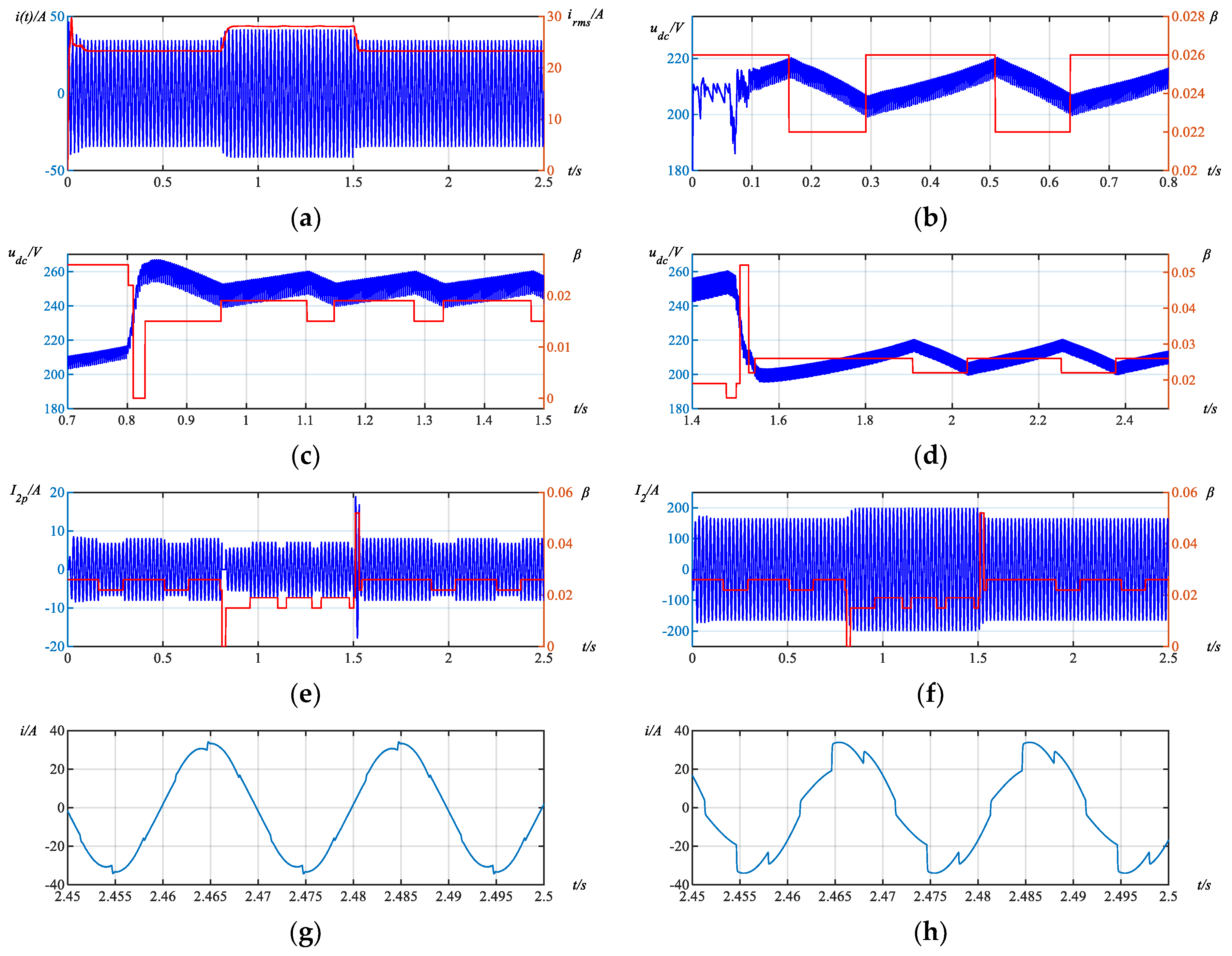
The simulation results are shown in
Figure 8. Specifically,
Figure 8a presents the simulation results of the system current. The blue line represents the instantaneous value of the A-phase system current, while the red line represents its RMS value. It can be observed that after the transition process at the beginning of the simulation, the system current stabilizes at 23.26 A. At
t = 0.8 s, a step increase in system current occurs due to a change in the triggering angle of the thyristor rectifier circuit. Since the RMS value is calculated for 50 Hz, the red line stabilizes at around 28.13 A after a fundamental period (0.02 s) delay, representing an increase of about 21% compared with the previous working condition. At
t = 1.5 s, the system current drops back to 23.26 A since the triggering angle of the thyristor reverts to the initial value.
To examine further the control effect of the DC voltage
udc, the entire 2.5 s simulation time is divided into three stages based on the variation of the thyristor triggering angle. The simulation results of
udc and
β are provided for each stage. In
Figure 8b, the results for the first stage (
t = 0~0.8 s) are presented. It can be observed that after
S1 opens at
t = 0.2 s,
udc is indeed controlled between 200 V and 220 V, and changes synchronously with
β. When
β is relatively large (
β = 0.026),
udc increases, and when
β is relatively small (
β = 0.020),
udc declines.
Figure 8c shows the simulation results for the second stage (
t = 0.8 s~1.5 s). In order to observe the dynamic effect, the simulation results for
t = 0.7 s~1.5 s are provided in
Figure 8c. When the thyristor firing angle is changed at
t = 0.8 s,
udc rapidly increases due to the delay effect of the fundamental current detection in the control system. However, the control system still considers this to be in the previous steady state. Therefore, when
udc reaches 220 V,
β decreases to 0.020. Subsequently, after half a fundamental period (0.01 s), the control system finds that the system current increases sharply and decides to restrain the excessive increase of
udc. Therefore, the control system sets
β to 0 and maintains it for one fundamental period (0.02 s). Simultaneously,
udc* is adjusted to 240 V and 260 V. It can be seen from
Figure 8c that during this transition process, the increase of
udc is suppressed. The maximum value of
udc is only 266.8 V. Compared to the control target, the overshoot is only about 2.6%. Subsequently, until
t = 1.5 s,
udc is stably controlled between 240 V and 260 V. It can also be seen that
udc changes synchronously with
β. When
β is large (
β = 0.019),
udc increases, and when
β is small (
β = 0.015),
udc declines.
Figure 8d shows the simulation results of the third stage (
t = 1.5 s~2.5 s). When the thyristor firing angle changes at
t = 1.5 s,
udc rapidly decreases due to the delay effect of the fundamental current detection in the control system. When
udc reaches 240 V,
β changes to 0.015. Then after half a fundamental period (0.01 s), the control system finds that the system current decreases sharply and decides to restrain the excessive decrease of
udc. Therefore,
β is set to a larger value of 0.05 and maintained for one fundamental period (0.02 s), while
udc* is reset to 200 V and 220 V. It can be seen from
Figure 8d that during this transition process, the rapid decrease of
udc is suppressed, reaching a minimum value of 195.6 V. Compared to the control target of 200 V, the deviation is only about 2.1%. Subsequently,
udc is controlled stably between 200 V and 220 V until
t = 2.5 s. Similar to the first two phases,
udc also changes synchronously with
β.
The transition process depicted in
Figure 8c,d indicates that the control requirements of the DC voltage
udc can be satisfied by changing the value of
β when the system current changes greatly. The steady-state control objective of
udc can be achieved, and the overshoot and deviation of
udc during the dynamic processes are also very small (not exceeding 2.6%). If larger overshoot and deviation are acceptable during the dynamic processes, then the variation of
β can be much smaller.
Figure 8e shows the relationship between the active current command
I2p of the A-phase inverter and the control parameter
β. It can be observed that
I2p and
β change simultaneously. Generally,
I2p remains very small. The typical peak value is no more than 20 A during the transition process. Furthermore, as the practical SHAPF prototype adopts a dual-winding configuration on the secondary side, and with a turn ratio of 10:1:1, the current in the secondary winding should be five times that in the primary winding. That means
I2p only accounts for about 2% of the total inverter reference current.
Figure 8f shows the total output current command value of the A-phase inverter. Due to the significant difference between the amplitude of
I2p and
I2q, as well as the 90° phase angle difference between them, the total output reference current of the inverter in
Figure 8f remains nearly unchanged with variations in the control parameter
β.
Figure 8g,h gives a typical filtering effect of SHAPF.
Figure 8g shows the steady state waveform of the A-phase system current after SHAPF is put into operation. The current RMS value is 23.26 A, and the total harmonic distortion (THD) is 3.77%. For comparison,
Figure 8h shows the steady state waveform of the A-phase system current by re-simulation with neither active power filter nor passive power filter. The current RMS value is 22.72 A, and the THD is 13.99%.
Figure 8g,h indicates that a good filtering effect is achieved.
The simulation results in
Figure 8 are in complete accordance with expectations, which proves that the DC voltage control method proposed in this paper is correct.
4. Experimental Verifications
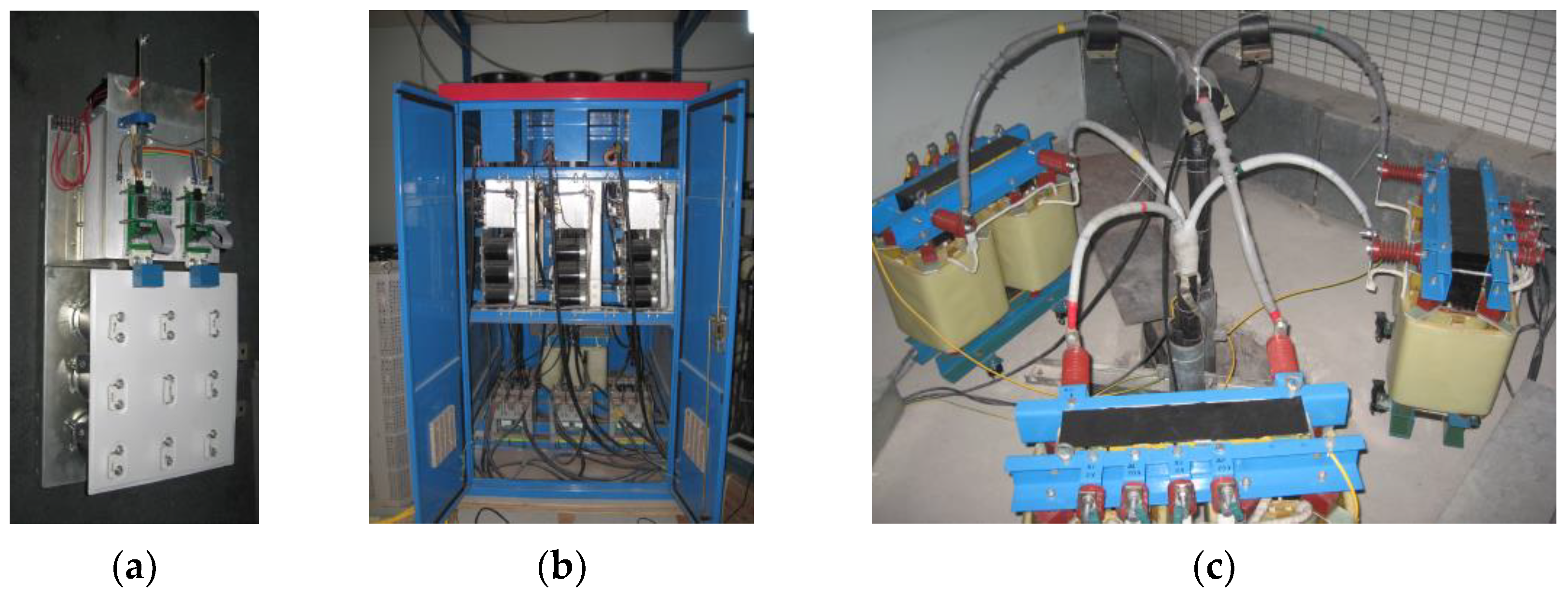
The SHAPF with MFC was applied in a 10 kV, 1 MVA factory in Guangdong Province, China. The basic configuration of the factory’s main circuit and the SHAPF prototype are shown in
Figure 5. The photos of the SHAPF prototype are shown in
Figure 9. Detailed descriptions of each parameter were provided in the previous section. Slightly different from the simulation circuit, the electric power supply charges the DC bus of the inverter through an autotransformer and a diode uncontrolled rectifier bridge. The DC voltage of SHAPF is controlled at around 240 V through the autotransformer. After the SHAPF is put into operation, the THD of the system current is no more than 3.2% under various operating conditions. The filtering effect is extremely good [
26]. During the maintenance period of this SHAPF prototype, the authors conducted validation experiments on this prototype to further validate the correctness of the proposed method. This means that this paper did not conduct any laboratory experiments in the laboratory, but instead used an actual model located in a factory for testing.
Since this SHAPF prototype was not designed with a DC voltage control function, there are no DC voltage sensor and signal modulation path in the control system. Therefore, automatic control cannot be realized during the experimental verification. Based on the existing conditions, this paper adopted the “manual control” method to verify the effectiveness of the proposed improved method, namely, whether the DC voltage of SHAPF prototype can be controlled to increase or decline. The correctness and feasibility of this improved method can be theoretically proven as long as the increase and decline of DC voltage are indeed achieved in the experiment.
The SHAPF prototype has a reserved external interrupt button on the main control circuit. Pressing the button will cause the main program to enter the external interrupt function. In normal working condition, this interrupt function is an empty function with no effect. Using this external interrupt achieves “manual control” by rewriting the external interrupt function, with the specific steps as follows:
- (1)
Retain the external ‘voltage regulator + rectifier bridge’ structure. In the initial state, use the ‘voltage regulator + rectifier bridge’ structure to maintain the DC voltage at around 80 V.
- (2)
Press the external interrupt button once, and the main program will enter the rewritten external interrupt function, set β = 0.04, which will cause an increase in DC voltage.
- (3)
After a certain period of time, press the external interrupt button again causing the main program to re-enter the rewritten external interrupt function and set β = 0.01. As a result, the inverter absorbs less energy, which leads to a decline in DC voltage.
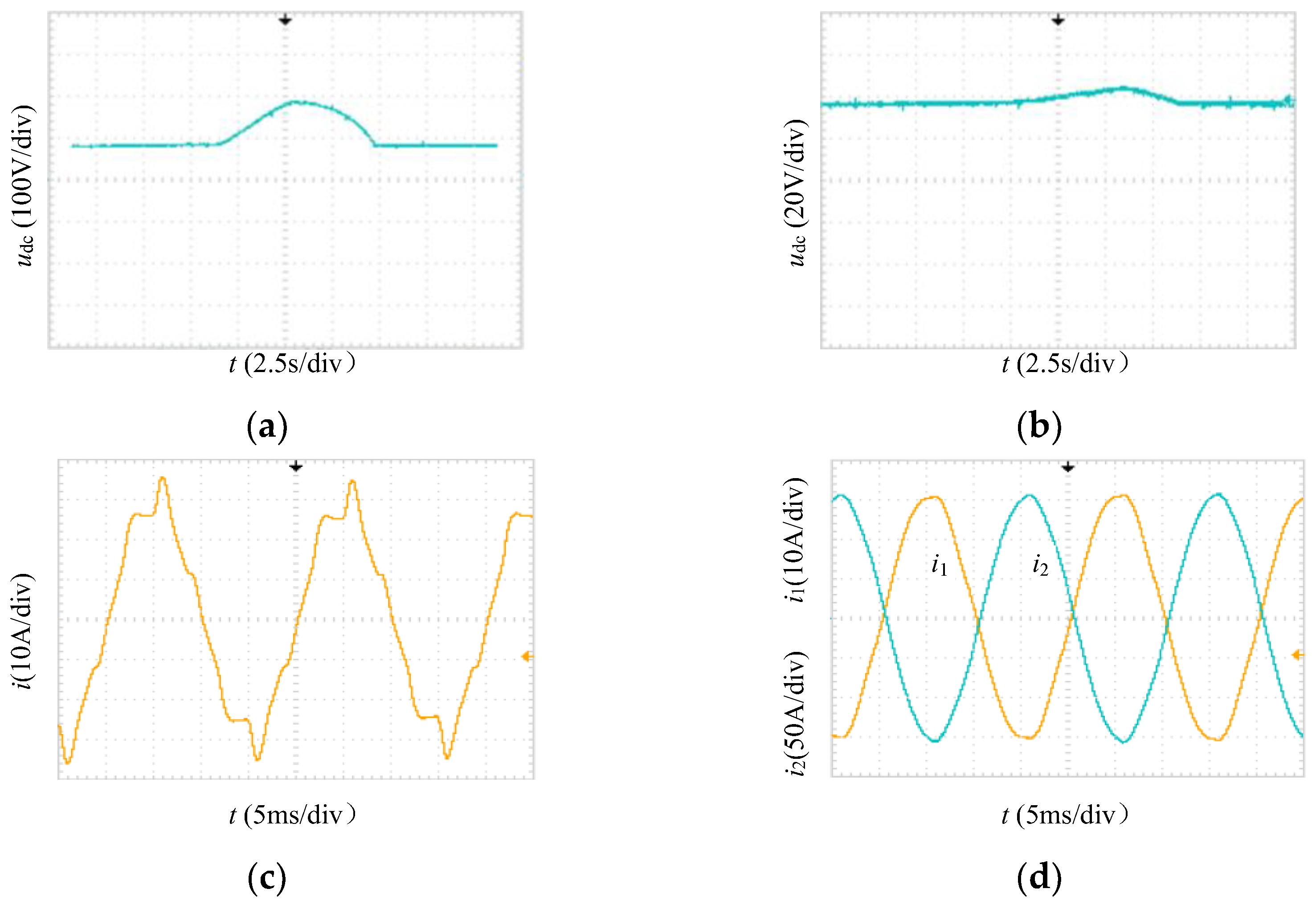
Figure 10 shows the experimental results.
Figure 10a illustrates the control effect of
udc. After receiving the external interrupt signal, SHAPF did achieve an increase in DC voltage that is higher than the output value of the “voltage regulator + rectifier bridge”. Upon receiving the external signal again, the SHAPF DC voltage declines. When the DC voltage drops to around 80 V, it is regulated by the ‘voltage regulator + rectifier bridge’ and remains stable. The experimental results are completely consistent with expectations.
Figure 10a illustrates another control effect of
udc. The output value of the “voltage regulator + rectifier bridge” is about 35 V. After receiving the external interrupt signal, SHAPF did achieve an increase in DC voltage. In
Figure 10b,
β = 0.034 and 0.012, which are less than the values (0.04) during the DC voltage increase process and larger than the values (0.01) during the DC voltage decline process in the manuscript. Therefore, the increase and decline of the DC voltages are slower. These results prove that the inverter’s absorbed power from the power grid and the control effect are indeed related to the control coefficient
β. Furthermore, the proposed method can control the increase and decrease of the DC voltage of SHAPF with different initial DC voltage values. By adding the corresponding hardware conditions such as DC voltage sensors and signal feedback block to the main control circuit of the SHAPF prototype, it can be upgraded from “manual control” to “automatic control”. There is no technical difficulty.
Figure 10c,d illustrates the filtering effect of SHAPF during normal operation.
Figure 10c shows the waveform of the A-phase current in the 10 kV system when only the passive filter is activated. The RMS current value is 20.99 A, and the THD is 13.08%. In
Figure 10d,
i1 represents the A-phase current in the 10 kV system after the active filter is activated. The RMS current value is 22.02 A, and the THD is 2.56%.
i2 in
Figure 10d represents the output current of A-phase inverter (due to limitations in the number of oscilloscope channels, only one inverter output current is provided), displayed in the antiphase. The RMS value is 109.35 A, and the THD is 1.31%. Additionally, it can be seen that the RMS value, THD and waveform of the system current during simulation are very close to the test results by comparing
Figure 10c,d with
Figure 8g,h. This proves that the simulation has a very good correspondence with the actual conditions.
It should be noted that the DC energy storage capacitance in the simulation circuit is only one sixth of the actual values. The smaller energy storage capacitor causes the DC voltage to increase and fall faster. This accelerates the simulation process, allowing for a shorter time to observe whether the DC voltage is under control. It verifies the correctness of the proposed method and the reasonableness of the
β value within a shorter timeframe. However, the downside is an increase in DC voltage ripple. This explains why the DC voltage changes more rapidly and has a larger ripple in the simulation results of
Figure 8 compared to
Figure 10a.
The improved method proposed in this paper has many obvious advantages compared to the conventional method in reference [
14], as shown in
Table 1. The main advantage is that in this improved method, the power absorbed by the inverter from the power grid
P is linearly related to the control coefficient
β, whereas in the method described in reference [
14], the relationship between these two factors is very complex. Therefore, if a faster dynamic performance is desired, the improvement method only needs to increase the value of the control coefficient
β to achieve the control objective. In contrast, the method in reference [
14] cannot determine whether the control coefficient should be increased or decreased.
