Article

Electrical Characterization of Boron Nitride-Filled Insulation for Aerospace and Avionics Applications

by
Gian Carlo Montanari
1,
Muhammad Shafiq
1,*,
Sukesh Babu Myneni
1,
Maricela Lizcano
2 and
Tiffany S. Williams
2
1
Center for Advanced Power Systems, Florida State University, Tallahassee, FL 32310, USA
2
NASA Glenn Research Center, Cleveland, OH 44135, USA
*
Author to whom correspondence should be addressed.
Energies 2024, 17(12), 3016; https://doi.org/10.3390/en17123016
Submission received: 3 May 2024 / Revised: 12 June 2024 / Accepted: 17 June 2024 / Published: 19 June 2024
(This article belongs to the Section F6: High Voltage)

Abstract

:
The environmental challenges associated with high-power, high-voltage electrified aircraft require a targeted approach with regard to the development of next-generation aerospace electrical insulation. This study reports findings on polyphenylsulfone (PPSU) as a matrix material based on its unique thermal, mechanical, and dielectric properties, filled with hexagonal boron nitride (h-BN) with micron- and nanoscale particulates. The inorganic ceramic filler was selected for its thermally conductive and electrically insulating performance in extreme environments. The main goal was to investigate the dielectric strength and electrical resistance (endurance) to partial discharges (PDs). Since PDs are a leading accelerated degradation phenomenon causing premature failure in organic electrical insulation, the capability of an insulating material to endure PD-induced degradation for the whole (or part of) its design life is of paramount importance. It was observed that incorporation of h-BN micro fillers can significantly improve the PD resistance, even in comparison with insulating materials typically used for electrified transportation, such as corona-resistant Kapton. It was also observed that a suitable combination of micro and nano fillers can also be used as a viable solution to increase the electrical performance and reliability of the avionics insulation components.

1. Introduction

Aerospace and avionics are moving towards an electrification future, and, in general, higher voltage and specific power, which implies larger electrical and thermal stresses. Since insulation life and reliability depend on the level and type of stress [1,2,3,4], insulation system design must address the aging rate for each type of stress and their combination, as well as the risk of incepting extrinsic aging mechanisms. The latter can be due to flawed design or mistaken operational stress level evaluation, changes in operation or modification of an electrical asset, poor manufacturing or commissioning, and aging effects [5,6]. Typical extrinsic aging processes are due to partial discharges (PDs) and hot spots, the latter of which result in fast, localized breakdown in both AC and DC insulation due to thermal instability generated by the exponential dependence of conductivity on temperature [7]. The former can trigger accelerated aging and premature breakdown owing to progressive dielectric material degradation caused by high-energy electron bombardment [8,9] (PD pulses are, in practice, high-energy micro-discharges occurring at the defect sites or on the surface [8,10,11]).
Developing insulating materials that can delay or even partially hinder extrinsic aging phenomena and at the same time allow the high-stress design of insulation systems would be, therefore, a must for the purpose of reaching high-reliability levels and specific power in electrified transportation and, in general, in any electrical asset component where the weight and volume must be minimized (it is noteworthy that insulation dimensions are mostly determined by electric and thermal stress, once voltage and loads are specified).
Unraveling PD degradation mechanisms can help in understanding the way to effectively engineer extrinsic-aging-resistant (EAR) materials. Electrical stress damage in organic insulators, i.e., the bond and chain dissociation process, is mostly associated with dissociative electron attachment (DEA) [12]. DEA scattering is the phenomenon where the energy of hot electrons (belonging to the avalanche that generates a PD pulse) is converted into chemical modifications of the dielectric. An example can be the dissociation of C-H bonds in hydrocarbon chains or aromatic rings, with the subsequent formation of free radicals and an H- ion and consequential removal of a hot electron from the conduction band. The DEA scattering rate would depend on temperature. It can be speculated that a decrease in local temperature due to better polymer thermal conductivity could shift to a higher energy in order for the conversion rate of hot electrons into chemical modification to occur (where the probability distribution of hot electron energy decreases). Thus, one can expect that damage due to, e.g., surface avalanches or PDs will decrease, diminishing the dielectric temperature. Referring to Figure 1, which reports the energy dependence of reciprocal effective scattering lengths for simple alkyl chains, with experimental results and model fitting (from [11,12,13,14,15,16]), with rising temperature, the electron–electron scattering curve would be shifted to the left (lower energy values due to thermal energy contribution), thus increasing the density of electrons able to cause damage. In addition to that, the higher temperature would also enhance the electron injection rate into the insulating material (from electrodes or internal defects), their extraction (AC and DC), and their transport (through increased conductivity, DC) [16,17].
This holds for organic materials. Bonds of inorganic materials are much stronger than hot electron energy put in place by the electron avalanches related to PD; thus, the bond-breaking action can be strongly delayed by inorganic particles embedded in the organic polymer matrix. This is the basic concept behind introducing nano or macro-fillers in organic materials where the presence of PD can drastically shorten life, as in the case of rotating machines (from corona-resistant motor wires to mica-paper tapes for generators).
Summarizing, increased thermal conductivity would likely diminish the extent of organic dielectric damage due to PD and the risk of thermal instability breakdown, but the most significant contribution to PD endurance would be obtained by introducing inorganic fillers that would reduce the damage growth, thus extrinsic aging rate.
This is the strategy driving the engineering and manufacturing of the inorganic micro- and nano-filled insulation characterized in this paper, that is, Polyphenylsulfone—Boron Nitride composite tapes [18,19]. As regards testing PD endurance, an innovative procedure is used in this paper, consisting of accelerated surface degradation testing. Upon designing an appropriate electrode which can generate a tangential field on the insulation surface large enough to trigger surface discharges, and having established an end point for the extent of surface degradation caused, at different voltages, mostly near electrode-specimen-air triple point, the extrinsic aging rate can be evaluated and compared among different types of materials [20].
Section 2 deals with material design and specimen manufacturing, in addition to describing testing procedures, the rationale behind accelerated surface erosion tests and an innovative PD measurement technique. Section 3 reports experimental results and the plots based on which PD material endurance can be compared. Eventually, a discussion on the validity of the approach and on diagnostic markers is developed in Section 4.

2. Materials and Experimental Procedures

The focus is on Polyphenylsulfone (PPSU) and its modified versions that are extruded with either micro-size or nano-sized hexagonal boron nitride (hBN), or a mixture of micro- and nano-sized hBN particles in a selected composition, Table 1. Multiple filler systems with different hBN particle size distributions were extruded and investigated to better understand the effects of platelet size and processing on thermal conductivity and insulation electrical properties [19]. The composites with the best electrical and thermal performance were down-selected and further investigated.
It should be noted that the use of a mixture of micro- and nanoscale fillers is a well-known method to optimize the thermal conductivity in filled composite systems, but there is also some research that has also shown improvements in dielectric performance when mixing both micro- and nanoscale filler sizes of hBN and other inorganic fillers [21,22,23,24]. The purpose of the research summarized in this paper was indeed to obtain and investigate composites that also show good PD resistance characteristics.
For the purpose of the testing presented in this paper, pristine PPSU, PPSU with nano BN, PPSU with micron BN, and PPSU with both micro and nano BN were extruded into tapes and collected on a sheet take-off accessory, similarly to the procedure followed in [18,19]. The thermal conductivity of the film specimens was measured at an outside facility using the light flash method and tested in conformance with ASTM E1461-13, “Standard Test Method for Thermal Diffusivity by the Flash Method” [25].
In addition to PPSU, a polyimide, i.e., Kapton in its corona-resistant version (PD resistant), was also tested for comparison while investigating the effect of nano and micro hBN PPSU fillers on dielectric breakdown voltage and resistance to partial discharges. As regards its resistance to PD, Kapton can be considered one of the most high-performance insulation products that is commercially available today and used in a variety of applications in aerospace and, in general, electrified transportation.
The tested PPSU materials are summarized in Table 1, together with their thermal conductivity. Tests were performed on a flat, extruded specimen of size 24 × 35 mm where the mean thickness of the PPSU specimens, with and without fillers, varied between 0.06 mm and 0.3 mm, while the mean thickness of the Kapton films was 0.05 mm. Since the new composite material evaluation was focused on short-term electrical breakdown (thermal instability) and long-term resistance to extrinsic aging (PD endurance), two types of test procedures were devised.

2.1. AC Breakdown Voltage Test

These tests were performed on 5 specimens for each type of material with a voltage ramp of 10 kV/min, until specimen breakdown. The test setup shown in Figure 2 was used. Figure 2a displays the electrode configuration. The diameter of the upper cylindrical electrode touching the specimen surface was 6 mm, while the bottom flat electrode had a diameter of 41.3 mm. The upper electrode was connected to high voltage, and the lower electrode was connected to ground. Figure 2b shows the experimental setup, including HV transformer, coupling capacitor, and test cell, and Figure 2c sketches its electrical layout. From these tests, an estimation of the breakdown (or electric) strength was obtained, roughly by dividing the breakdown voltage by the insulation thickness at the breakdown location. A model based on thermal-breakdown physics was used to homogenize breakdown strength results obtained on specimens of different mean thicknesses (next section).

2.2. PDIV and Surface Erosion Tests

The experimental study related to PD performance consisted of measuring first the mean partial discharge inception voltage (PDIV) and secondly the PD-induced surface erosion rate of each material.

2.2.1. AC Partial Discharge Inception Voltage

PDIV measurement is a well-known testing technique that is applied typically as a tool during insulation system diagnostics. In this study, AC PDIV investigation played a central role when applied to flat insulation specimens for which PDIV is practically determined by electrode shape, insulating material dielectric constant (in AC), and specimen thickness. First, the voltage level (in terms of multiple of PDIV) applied during PD surface erosion tests to study material performance under accelerated aging conditions could be established. Second, in-depth analysis of the type of PD activity at the start (t = 0 h) of the surface erosion test (surface or internal discharge) at PDIV unraveled the type of mechanism causing surface erosions and precisely whether, as expected, it consisted of surface discharges or involved gas discharges at electrode contours. As discussed later, an interesting metric, i.e., the transition of the likelihood of PD typology from surface to internal, can help in evaluating the capability of the tested materials to endure partial discharge (PD). Modeling partial discharge inception field and voltage is also a valuable tool to design test electrodes and PD-free insulation systems, as seen in the next section.
(a)
Generalized Partial Discharge Inception Model
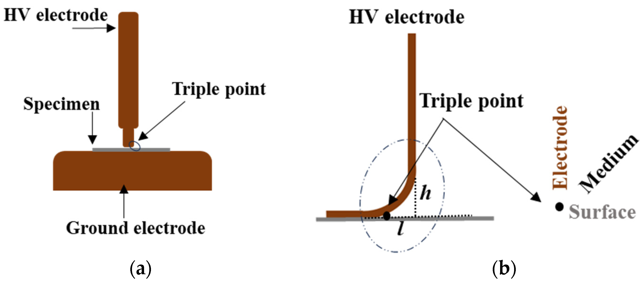
Let us consider the electrode configuration and its contour shown in Figure 3, which are those pictured in Figure 2a,b. The triple point (electrode, surface, and surrounding medium) play an important role in the type of PD inception mechanism. Indeed, two different discharge processes could potentially be incepted with the chosen electrode profile. The first is surface discharge, that is driven by a tangential field along the horizontal direction, l, over the specimen surface. The second is the gas discharge between the HV electrode and insulation surface, occurring in the orthogonal direction along h, which can be identified as an internal discharge (since the phenomenology and physics are similar to those of discharges in insulation bulk defects). A detailed study on surface and internal discharges developed at the electrode–specimen interface is presented in [20].
Recalling that it is the electric field that promotes PD, not the voltage, calculations of the surface discharge PD inception field, PDIE, can be carried out using a new model that works for both internal and surface discharge [20,26,27]:
E i = 8   p   1 + 4.3 p k s l 1 / 2
valid for air at pressure p, where l is the distance between the high voltage (HV) and ground (from triple point to specimen border in Figure 3), and ks is a parameter based on the electric field profile, see Figure 4. An expression for ks, based on the extent of the field gradient at the triple point and, thus, on the effective streamer length, is given by [27]:
k s = l 0.9 E m a x l 0.9 E m a x + l
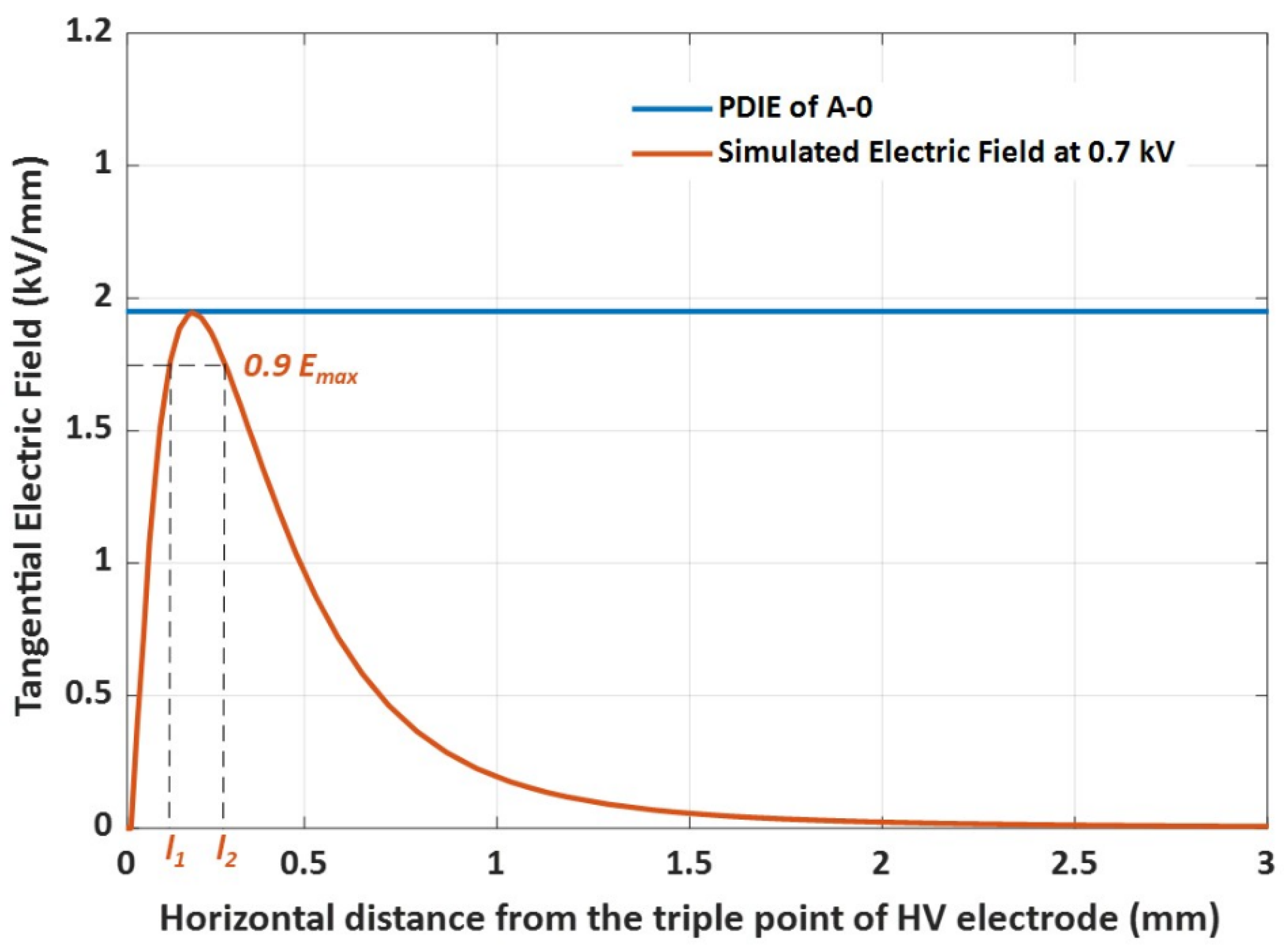
where Emax is the maximum value of the tangential surface field as obtained from the electric field profile calculation. Figure 4 shows how the surface partial discharge inception field (PDIE) and the PDIV are obtained by the match of the simulated tangential electric field profile peak with the PD inception field value provided by model (1). Since the intersection of the simulated field (by COMSOL) and model (1) occurs at 0.7 kV for the specimen A-0, the PDIV of A-0 is determined as 0.7 kV. The validity of the model for the tested specimens can be observed by comparing the theoretical PDIV in Table 2 and experimentally measured PDIV values in Table 3, where it is shown that estimated and measured values almost coincide.
Modelling PDIE and considering size effect (as in [28]) would allow the voltage level for accelerated surface erosion tests to be determined, which is meant to be a multiple of PDIV for each material, to be scaled up with insulation thickness, in order that the tests are performed referring to a multiple of the inception field for each type of specimen. In other words, referring to Table 2, the test voltage was taken as that corresponding to a multiple of PDIE for each specific specimen. For example, comparing Kapton CR and sample C-6.1-m+n, erosion tests performed at 3 times the PDIV yield drastically different test voltage values, e.g., 1.5 and 3.3 kV, respectively. As a note, it can be seen from Table 1 and Table 2 that by adding 1 wt% nano-BN in the unfilled (neat) PPSU, the relative dielectric constant (measured by a precision impedance analyzer at 0.5 V, 62 Hz) is increased from 2.93 to 3.39 (measured at 64.2 Hz). A larger filling, i.e., 6.1 wt% (micro + nano) BN and 14 wt% micron-BN, exhibits some increase in the dielectric constant, to 3.63 and 3.68, respectively, which then remains almost constant upon further increasing the nano and micro filler concentrations.
(b)
PD Measurements
A variable AC supply was connected across the electrode cell. A high-voltage coupling capacitor was used as voltage divider in order to provide a synchronization signal to the PD measurement unit so that PD pulse time/phase occurrence could be put in relation to the applied AC sinusoidal supply. A high-frequency current transformer (HFCT) was used as the PD sensor, mounted on the ground connection, i.e., in series with the test cell (to sense PD pulses going from the specimen surface towards the ground link). The experimental setup is sketched in Figure 5. The HFCT was connected to an innovative, fully automatic PD detector equipped with analytics software that was able to identify the type of source generating the PD (discussed in Section 3).
The PDIV was determined by gradually increasing (at a step of 50 V) the applied voltage until PD signals were observed. The PDIV value corresponded to the voltage at which the permanent inception of PD was observed. Mean measured PDIV values for each material are presented in Table 3.

2.2.2. Surface Erosion Tests

Having measured PDIV, accelerated surface erosion tests could be performed at constant voltage, whose amplitude was a selected multiple of PDIV for each material. In this paper, the data refer to test voltage = 3PDIV applied for a duration of 8 h. Surface erosion tests would allow direct evidence of the capability of the composite to thermalize the electron energy and reduce the rate of insulating material bond breakage.
During accelerated surface erosion tests, partial discharges were monitored at selected times (typically, on an hourly basis). Similarly, at selected hours, the specimens were taken out of the surface erosion test cell to perform surface roughness measurements.

3. Experimental Results

3.1. Breakdown Strength

Table 3 summarizes the results of the breakdown voltage (BV) tests (along with PDIV). Based on the measured breakdown voltage, the breakdown strength (BS) was approximately calculated with reference to the thickness of the breakdown point (location) on the specimens, assuming uniform field distribution.
As seen in Table 3, the thickness of the breakdown point varied significantly for different specimens (by as much as three-fold when comparing Kapton CR with C-6.1-m+n). This required a correction of the calculated electric (breakdown) strength considering the contribution of different volumes at the failure point for the same failure area. In other words, the effect of volume heat accumulation vs. surface heat dispersion must be leveraged to compare the results in an unbiased way. For this purpose, the dependence of BS on thickness d is given by [28]:
BS = K d −1/2
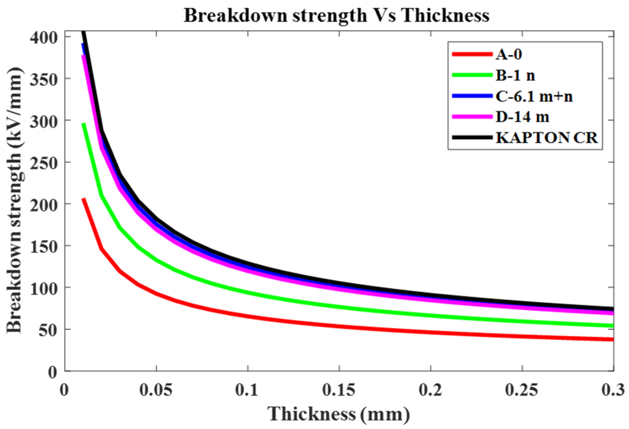
where K = ε λ Δ θ ω t a n δ 1 2 , while ε′ is relative dielectric constant, λ = thermal conductivity, Δθ is temperature drop, ω = 2πf with f as frequency of the applied voltage, and tanδ is dissipation factor. Based on (3) and Table 3, Figure 6 reports the breakdown strength for each type of material up to the maximum thickness of 0.3 mm. As can be seen, referring, e.g., to insulation thickness of 0.2 mm, the value of Kapton CR breakdown strength was very close to those of samples D-14-m and C-6.1-m+n, which were micron-filled and micron + nano-filled specimens, respectively. Considering PPSU specimens, there was a considerable increase in the BS of sample B-1-n as compared to sample A-0 (neat specimen). Similarly, the BS of specimen C-6.1-m+n with 6.1 wt% micro + nano BN was larger than that of D-14-m with ~14 wt% micron BN. Comparing specimens C-6.1-m+n and D-14-m, although D-14-m had a greater concentration of 14 wt% micro-filler, sample C-6.1-m+n had a slightly higher BS due to the addition of a mix of nano and micro fillers. Similar behavior could be seen when observing the breakdown voltage of the respective materials for the same thickness of 0.2 mm (Figure 7). This indicates that for realistic insulation thickness for MV application, micro and micro + nano filled materials can behave as the target material (Kapton CR).

3.2. PDIV and Surface Erosion Test Results

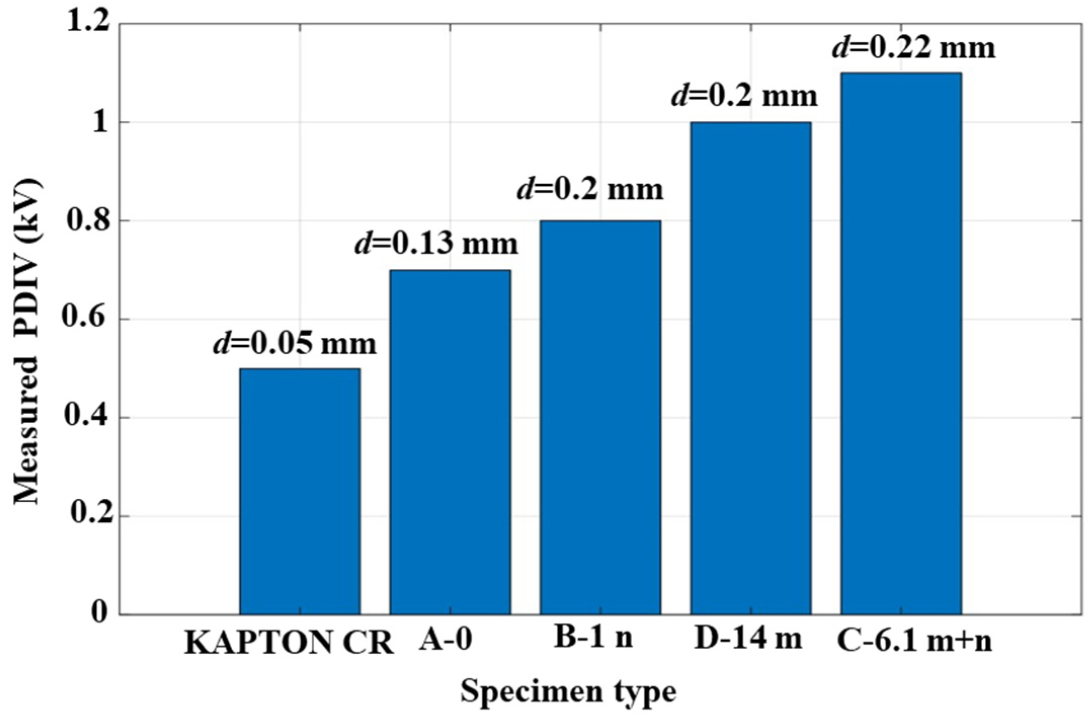
PDIV values are plotted in Figure 8 together with mean thickness, d, for each type of material. It is seen that with increasing thickness, PDIV also increases, which is predictable since, roughly, if the inception field is almost constant, Equation (3), then inception voltage varies with the ratio d/ε′. It can be speculated that the effect of the dielectric constant is less important than that of thickness in our case, since dielectric constant variations are much smaller than those of thickness.

3.2.1. PD Monitoring during Surface Erosion Test

As mentioned, PD measurements and analytics were performed by using an automatic, unsupervised innovative PD detection system with separation, recognition, and identification (SRI) capability. In analyzing PD measurement results measured in the form of phase-resolved partial discharge (PRPD) patterns, noise needed to be separated from PD, recognized, and rejected in order to be able to extract partial discharge sub-patterns and identify the type of source generating PD. Separation was accomplished by procedures that clustered the acquired PD pulses based on signal processing using principal component analysis (PCA) [29,30]. Recognition was based on the statistical tests performed on PD pulse characteristics and properties relevant to each cluster, in order to achieve sub-patterns and recognize those related to the noise and PD [30]. The final step was the identification of the type of source generating PD, as a fundamental tool for the purpose of diagnostics and condition assessment. Various markers were considered by a fuzzy logic-based approach, according to which PD could be primarily identified as belonging to three categories, i.e., the internal, surface, and/or corona discharges. A number in the range 0 to 1 was associated with the identification, expressing the likelihood of each category (which was a direct consequence of the use of a fuzzy logic engine).
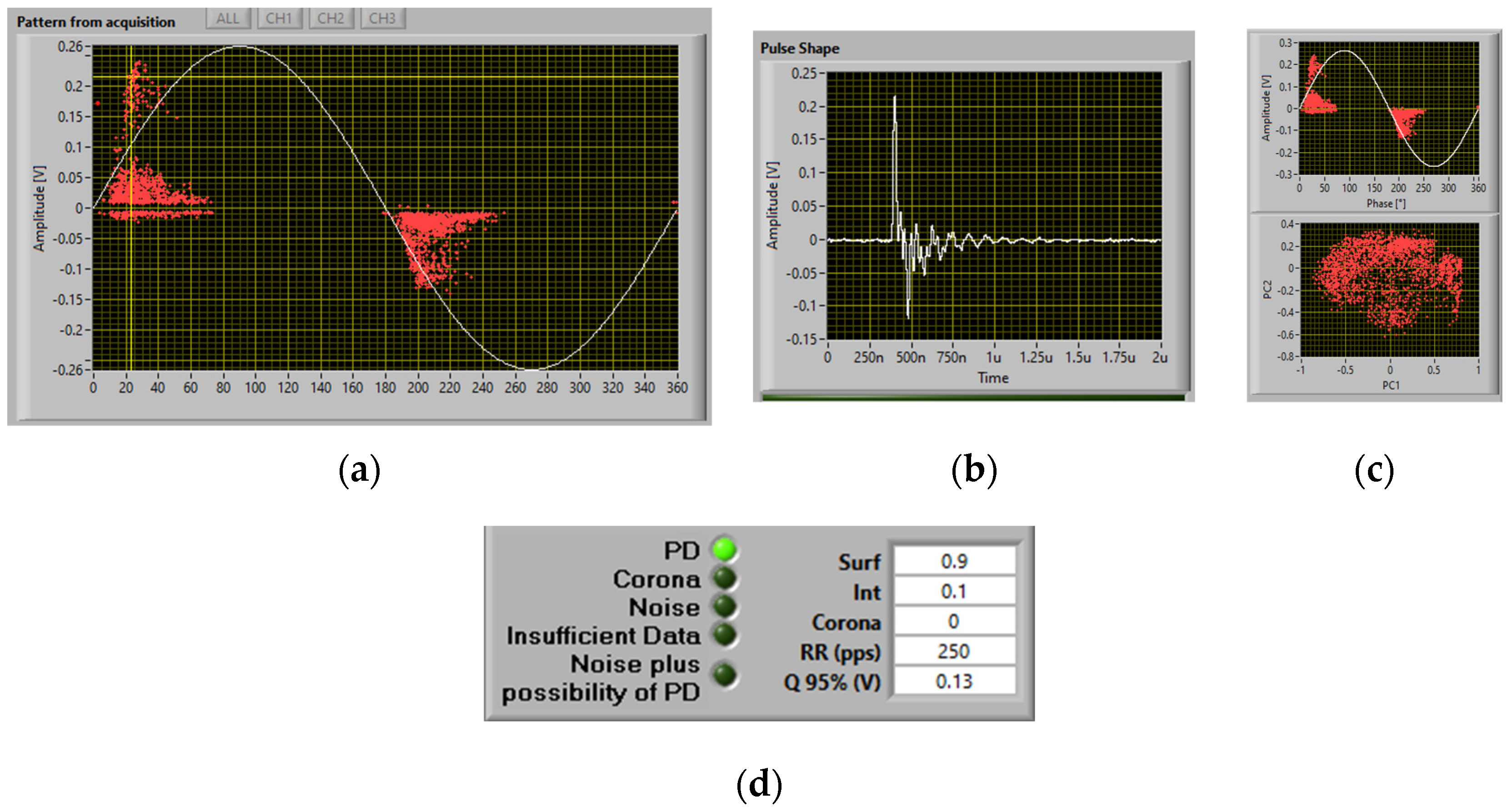
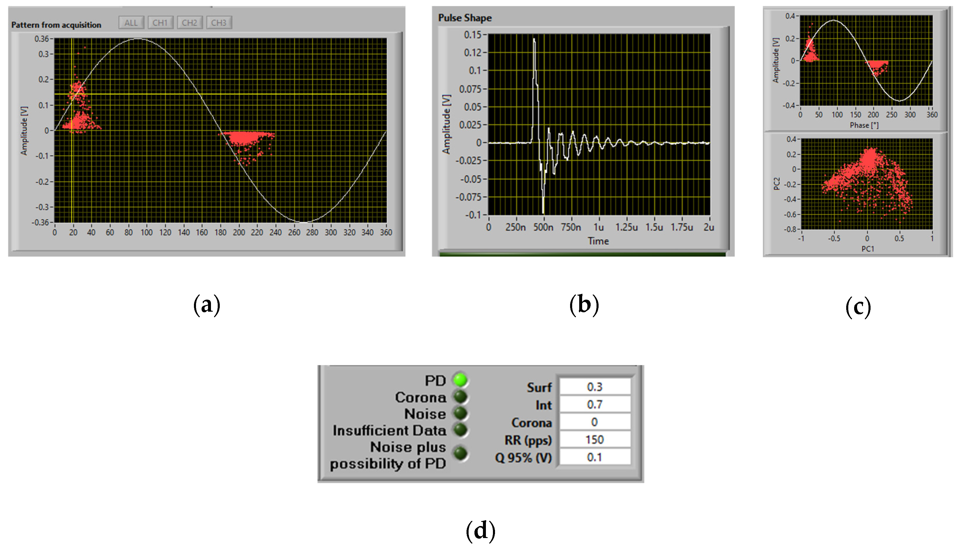
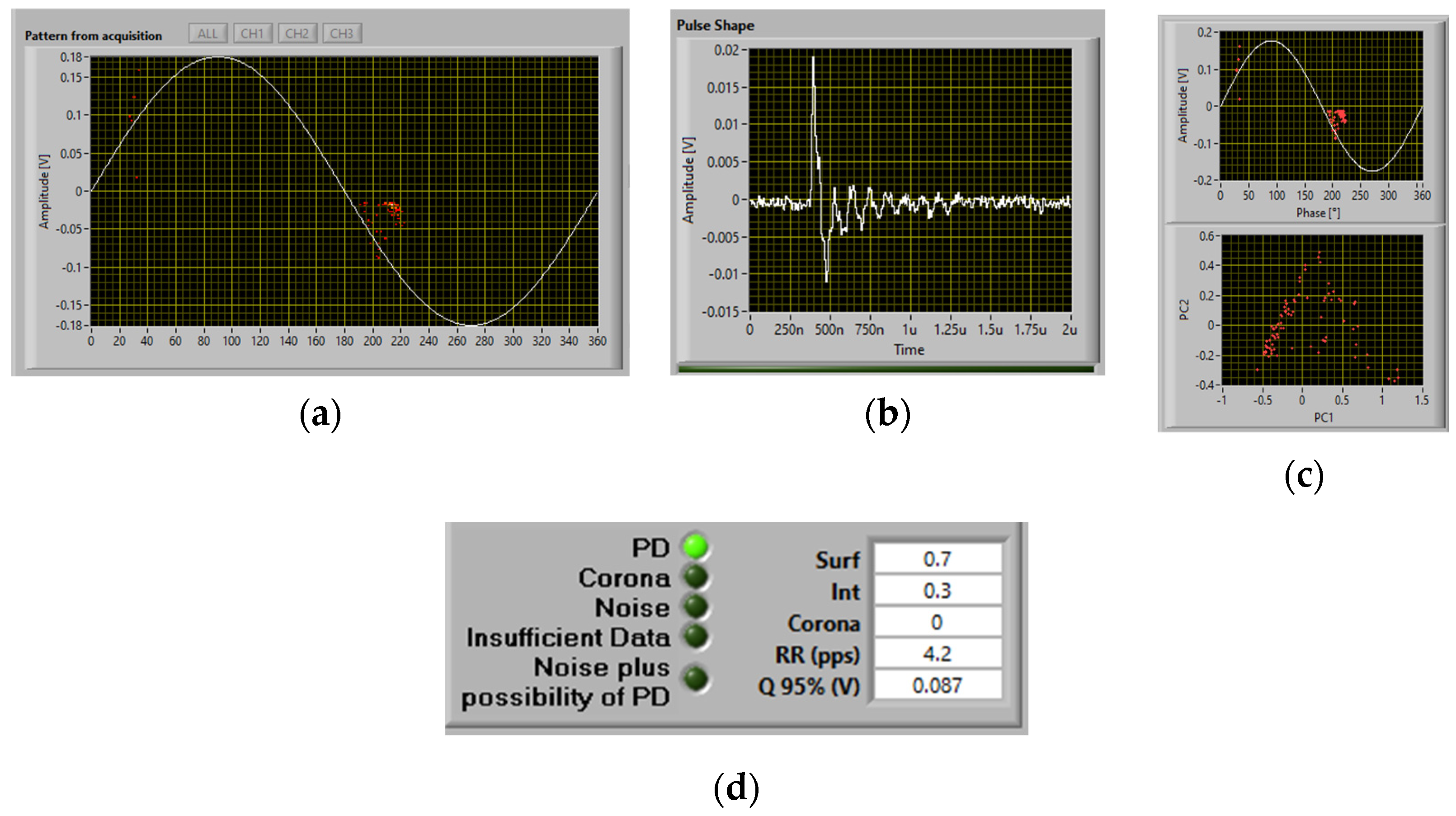
During accelerated erosion tests that lasted for 8 h, PDs were monitored on an hourly basis. Examples of PD measurements for the neat specimen A-0 and specimen D-14-m are presented in Figure 9, Figure 10, Figure 11 and Figure 12. These figures report excerpts of a typical screenshot of the software analytics, automatic and unsupervised, consisting of global phase-resolved PD (PRPD) pattern, typical PD pulse, separation (PCA) map with clustering, and identification of the type of PD with the related likelihood (e.g., in the case of Figure 9, 90% surface and 10% internal).
Figure 9, Figure 10, Figure 11 and Figure 12 show the results of PD measurements at the beginning (considered as 0 h) of an erosion aging test and after 8 h of aging, on specimens A-0 and D-14-m, respectively.
It is interesting to note that for the neat specimen A-0, the PD identification shifted from mostly surface PD (0.9, i.e., 90%, with internal PD of 10%) on the unaged specimen, Figure 9, to mostly internal PD (0.7, i.e., 70%) after aging of 8 h, Figure 10.
For the micro-filled specimen D-14-m, Figure 11 indicates that PD activity for the unaged specimen was identified entirely (100%) as surface discharge, while after 8 h of accelerated aging (thus surface erosion), PD activity was identified as 70% surface and 30% internal (Figure 12).
A common feature of all specimens subjected to surface discharge-accelerated aging, derived from PD monitoring, is that PD source typology identification shifts from almost purely surface to largely internal. This can be explained by speculating that surface damage occurring during aging would erode the tested materials starting from the surface and then penetrate through semiconductive pits into the bulk. The electric field in the pits would have a predominant orthogonal component (unlike that driving surface erosion, which is tangential), and be magnified at pit tips, resulting in a gradual increase in the internal discharge activity. This can be highlighted by microscopic observations, as shown in Figure 13 and confirmed by the shorter failure times for those specimens having lower surface discharge resistance (as discussed in the next section).
Such results suggest that the transformation of the discharge activity from predominantly surface discharge to gas/internal discharge could be a useful metric in evaluating the impact of the degradation for the insulation system surface. This can be highlighted (and quantified) by resorting to the correlation between the likelihoods of surface and internal PD, which can be expressed by:
L(PD%sur) = 100 − L(PD%int)
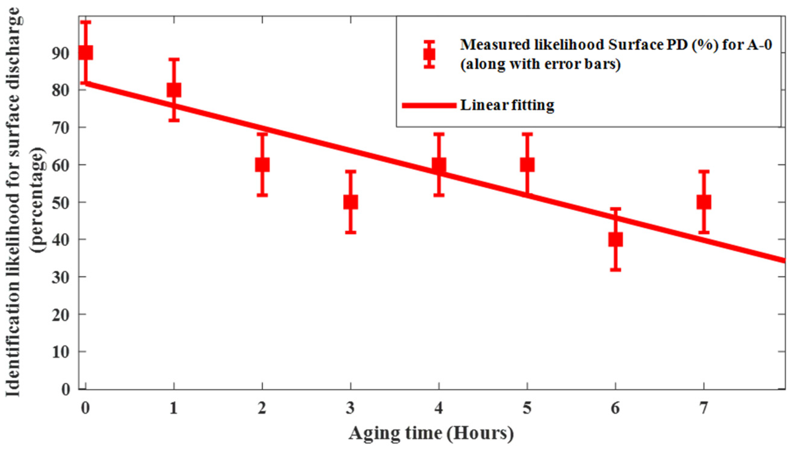
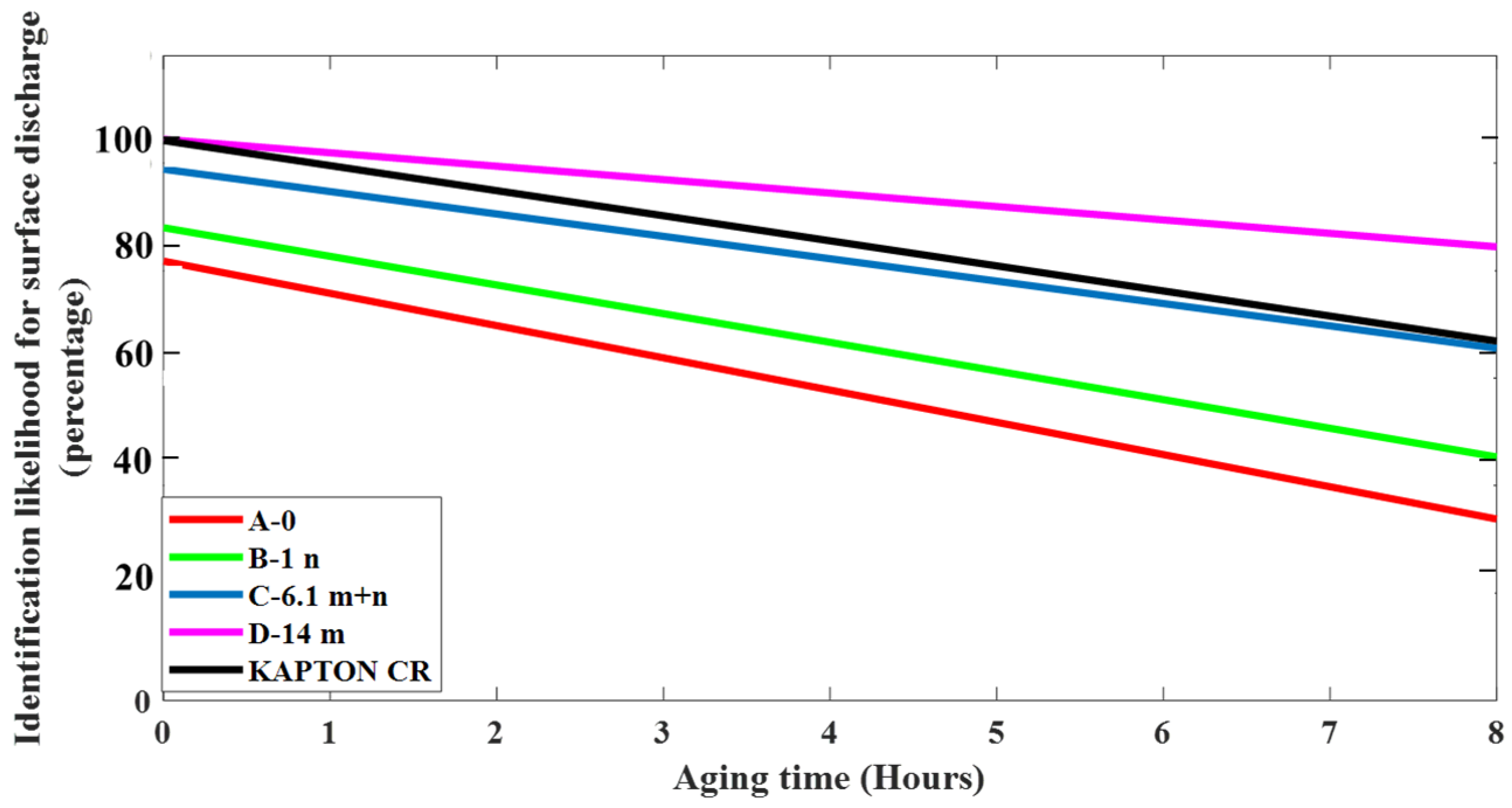
where L(PD%sur) and L(PD%int) are the likelihoods of surface and internal PD, respectively, relative to aging time: the lower the correlation line slope, the better the material PD endurance. Figure 14 presents an example of the time behavior of surface PD identification likelihood with aging for the neat specimen A-0, which looks reasonably linear. The identification likelihood (Equation (4)) plots vs. aging time for all tested materials are presented in Figure 15, indicating that those materials having better resistance to PD are D-14-m and Kapton CR. This result will be validated in the next section, based on surface erosion measurement results.
Dealing with PD magnitude and repetition rate, it is shown in [31] that PD magnitude and repetition rate decrease with aging for most materials, which may be due to the progressive surface deterioration, increase in surface conductivity, and roughness.

3.2.2. Surface Roughness Measurements

During surface erosion, the discharge activity causes physical degradation to the texture of the surface that can be quantified by the measurement of surface roughness. Surface roughness measurement was carried out for each material based on Ra (arithmetic average roughness) over a specified area around the position of the electrode placed on the specimens for accelerated aging. Roughness can be measured by a profilometer supported by an optical microscope (in our case, magnification of 20× was used for most of the images), as the vertical deviation of the texture of the surface from the undisturbed surface of the under-test specimen. During accelerated surface erosion tests, it was expected that surface roughness would increase with time.
Surface roughness was measured in the neighborhood of the electrode location (Figure 2a), extending outward up to a suitable distance all around the electrode, collecting several measurements, and then calculating the mean value at specified times during aging (i.e., at 0 h, 3 h, 5 h, 7 h, and 8 h).
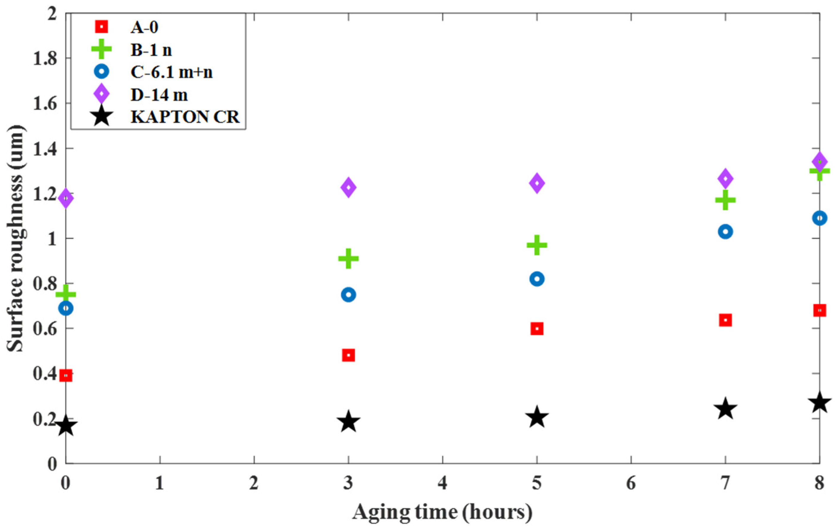
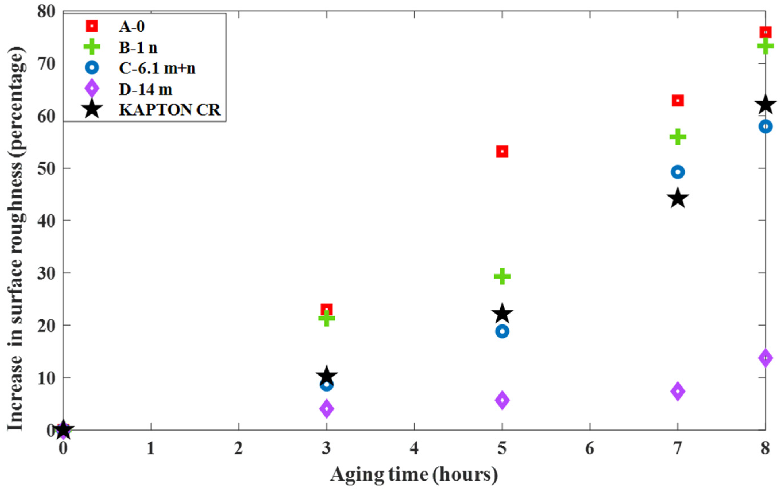
Figure 16 summarizes the results of the surface roughness measurements, while the rate of change in surface roughness, derived from Figure 16, is presented in Figure 17. As can be seen, the PPSU materials, especially those with micro or mixed micro and nano-filler, seemed to behave as well as, or better than, the Kapton corona resistant one.
Surface roughness can actually be considered the key metric for evaluating the aging performance as a result of surface erosion. Comparing all the tested specimens, the unfilled specimen A-0 displayed the highest percentage increase in surface roughness, while the specimen with 14 wt% micro-BN, the composite specimen D-14-m, had the lowest increase in the surface roughness, thus the best PD aging performance.
The most striking result was that the performance of specimen D-14-m was better than that of Kapton CR, while specimen C-6.1-m+n and Kapton had approximately similar behavior.

4. Discussion

The outstanding results from the accelerated surface erosion tests showed that all PPSU specimens, both with and without micro/nano-fillers, had good resistance to PD, and some were even better than the commercial-grade Kapton corona resistant specimen. It seems that the addition of nanofiller can improve the resistance to PD, but not as well as the micron-BN filler at ~14 wt% loading. An explanation could be that the BN platelets can delay the damage induced by PD. Partial discharge pulses can hit material (surface in our test arrangement) with an energy distribution up to 100 eV [16], which can easily break typical polymer bonds. However, this energy is not large enough to generate damage in inorganic fillers; thus, introducing micro fillers would delay the entire damage process. The effect of nanofillers could likely be enhanced by increasing their concentration and reaching exfoliation conditions, which would increase interaction with the host material [32,33]. A further contribution to PD resistance could be provided by the high thermal conductivity caused by enhanced phonon transport in the composites.
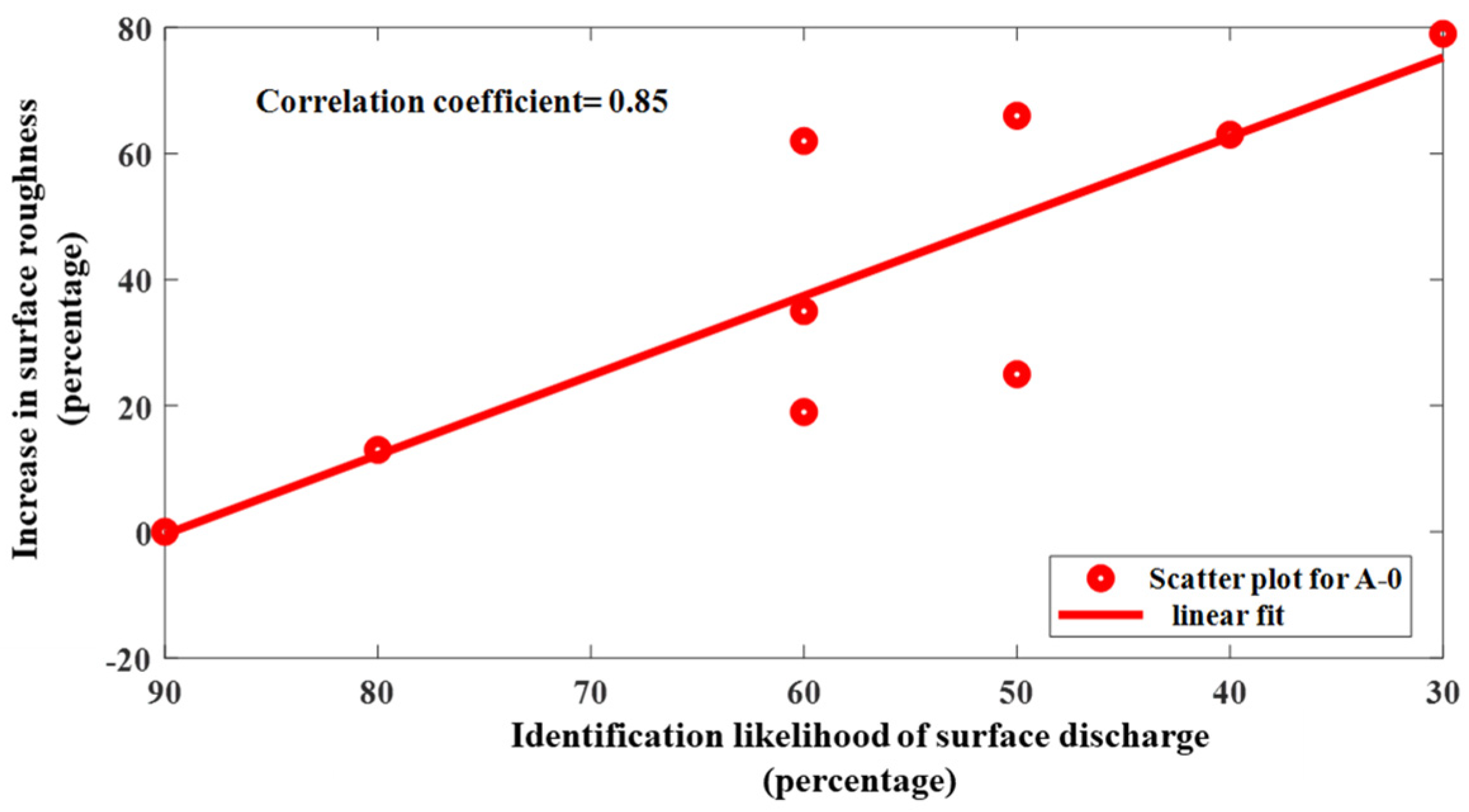
Regarding PD measurements, it is interesting to note that identification shifted from mostly surface PD on new specimens to mostly internal PD as aging time increased, as shown in Figure 14 and Figure 15. Such behavior is due to the progressive degradation of the specimen surface, which tends to generate conductive pits that penetrate the specimen in the direction of the orthogonal field. The high field at pit tips will cause insulation breakdown. It can be speculated, then, that the likelihood of identification could be a diagnostic indicator of insulation surface aging and approaching breakdown. Figure 15 highlights, indeed, that the micron filled material has a lower drop in likelihood after 8 h of aging, compared to the unfilled and nano filled specimens. This is in agreement with the results of surface roughness measurements, Figure 16 and Figure 17, and it is clearly supported by Figure 18, where surface roughness (percentage increase) is plotted as a function of identification index for one of the tested materials, specimen A-0. As can be seen, correlation is good (0.85), for a decreasing trend of both erosion and surface likelihood identification. The correlation coefficient (CC) was >0.7 for all tested materials.
As aging indicators related to on-line PD measurement/monitoring, the product of PD magnitude, Ai (t), and repetition rate, rri (t), can be plotted as functions of aging time for each material i. These can serve as metrics of the extent of insulation cumulative extrinsic stress causing surface erosion:
CESi (t) = Ai (t) · rri (t)
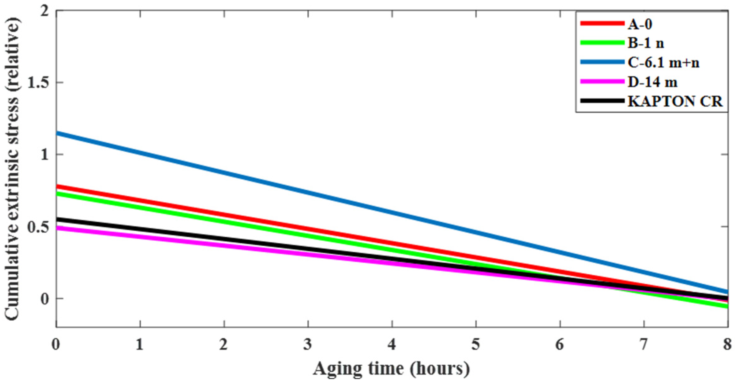
where CES refers to cumulative extrinsic stress. The relationship between this quantity and the damage rate can help in understanding the capability of a material to withstand PD. CESi (t) plots are displayed in Figure 19, referring to the PD amplitude and pulse repetition rate obtained for all tested specimens during 8 h of accelerated aging. Extrinsic stress decreases with aging time because of the transition from surface phenomena, characterized by large-amplitude partial discharges, to internal phenomena, the latter featuring small-magnitude discharges (matching the identification obtained from PD analysis (surface vs. internal, Equation (4)).
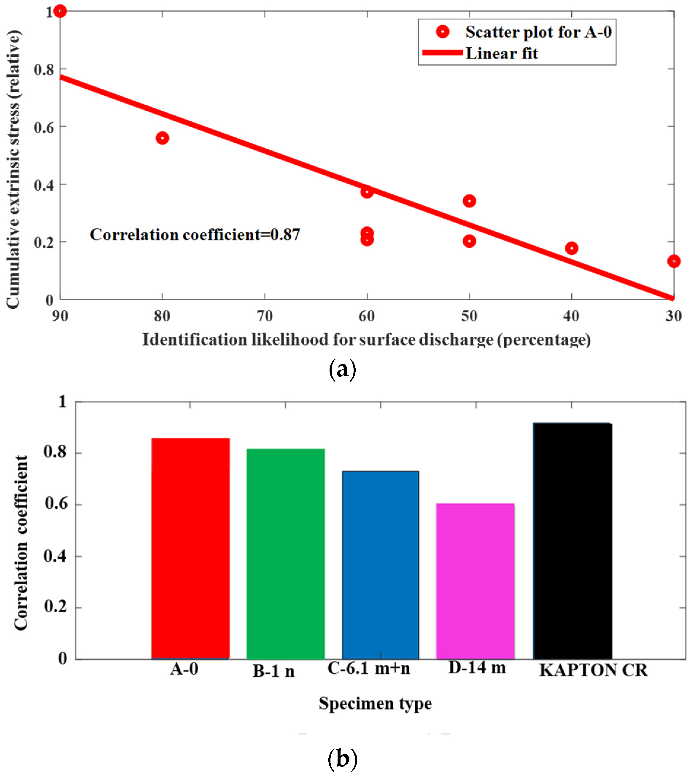
The validity of the CES and PD identification likelihood as aging-resistance metrics is highlighted in Figure 20, where CES is correlated to the likelihood of surface discharge (which has been proven to be a good aging marker, Figure 18). Figure 20 indicates that the CES marker decreases with aging time, displaying a reasonably good correlation coefficient (the collection of CC values is reported in Figure 20b for all tested materials). This can provide a further evaluation tool for the PD resistance of a material.
Finally, it can be observed that accelerated erosion tests are quick and provide much more insight into the phenomenology of degradation mechanisms and PD behavior than conventional accelerated life tests prolonged until insulation failure [1,5]. They can be considered as a good candidate for a standard procedure for insulating material characterization when PD is a central event in potential service aging mechanisms.

5. Conclusions

This work indicates that PPSU filled by micro-structured BN platelets is a promising material for insulation of electrical equipment, especially where weight/volume constraints would require high design fields, high operating temperature, and improved endurance to extrinsic aging due to partial discharges. Indeed, such characteristics portray electrified transportation applications, where reaching the highest specific power with no compromise in reliability is a must.
The high breakdown strength may suggest a promising high value of design field (but accelerated life tests are needed to confirm this speculation), and the very good resistance to surface discharges could allow designing an insulation system that does not lose reliability, or life, even if PDs are incepted during operation. This concept could be named a “reliability redundant” design, where redundancy is due to the fact that even if the design is PD-free, the appearance of PD would not affect the specified life and failure probability. In the case of aircraft and aerospace applications, the inception of PD during cruise, due to significantly reduced PDIV at lower atmospheric pressure, is an event that cannot be ruled out or easily predicted at the design stage, especially if aging, change of mission, unexpected stresses, or harsh environmental conditions may take place. Even if more work is needed to investigate erosion behavior and PD phenomenology at reduced atmospheric pressure, the results reported here indicate that the investigated materials could be extremely useful in reduced pressure applications.

Author Contributions

Conceptualization, G.C.M., M.L. and T.S.W.; methodology, G.C.M.; software, G.C.M., M.S. and S.B.M.; validation, G.C.M., M.S. and S.B.M.; formal analysis, G.C.M., M.S. and S.B.M.; investigation, G.C.M., M.S. and S.B.M.; resources, G.C.M., M.L. and T.S.W.; data curation, M.S. and S.B.M.; writing—original draft preparation, G.C.M., M.S. and M.L.; writing—review and editing, M.L. and T.S.W.; supervision, G.C.M.; project administration, G.C.M.; funding acquisition, G.C.M. and M.L. All authors have read and agreed to the published version of the manuscript.

Funding

This research was funded by NASA’s Transformational Tools and Technology Project under the Foundational Electrified Aircraft Propulsion Sub-Project, contract/grant number 80NSSC22PB528.

Data Availability Statement

Data are contained within the article.

Conflicts of Interest

The authors declare no conflicts of interest. This manuscript is a joint work of employees of the National Aeronautics and Space Administration and employees of Florida State University under Contract/Grant No. 80NSSC22PB528 with the National Aeronautics and Space Administration. The United States Government may prepare derivative works, publish, or reproduce this manuscript and allow others to do so. Any publisher accepting this manuscript for publication acknowledges that the United States Government retains a non-exclusive, irrevocable, worldwide license to prepare derivative works, publish, or reproduce the published form of this manuscript, or allow others to do so, for United States government purposes.

References

  1. IEEE 930/IEC 62539; IEEE Guide for the Statistical Analysis of Electrical Insulation Breakdown Data. IEEE: Piscataway, NJ, USA, 2007.
  2. IEC 60216; For the Determination of Thermal Endurance Properties of Electrical Insulating Materials. Parts 1–7; IEC: Geneva, Switzerland, 2013.
  3. Montanari, G.C. Notes on theoretical and practical aspects of polymeric insulation aging. IEEE Electr. Insul. Mag. 2013, 29, 30–40. [Google Scholar] [CrossRef]
  4. Dumbar, W.G. HV design guide: Aircraft. Boeing Report, AFWAL-TR-82. January 1983. [Google Scholar]
  5. IEC 60505; Evaluation and Qualification of Electrical Insulation Systems. 4th ed. IEC: Geneva, Switzerland, 2011.
  6. Montanari, G.C.; Seri, P.; Morshuis, P.; Hebner, R. An approach to insulation condition monitoring and life assessment in emerging electrical environments. IEEE Trans. Power Deliv. 2019, 34, 1357–1364. [Google Scholar] [CrossRef]
  7. Seanor, D.A. Electrical Properties of Polymers; Academic Press: London, UK, 1982. [Google Scholar]
  8. Kreuger, F.H. Partial Discharge Detection in High-Voltage Equipment; Butterworth-Heinemann: Oxford, UK, 1990. [Google Scholar]
  9. Montanari, G.C. Aging and life models for insulation systems based on partial discharge detection. IEEE Trans. Dielectr. Electr. Insul. 1995, 2, 667–675. [Google Scholar] [CrossRef]
  10. IEC 60270; High-Voltage Test Techniques—Partial Discharge Measurements. Edition 3.1; IEC: Geneva, Switzerland, 2015.
  11. Montanari, G.C. Bringing an insulation to failure: The role of space charge. IEEE Trans. Dielectr. Electr. Insul. 2011, 18, 339–364. [Google Scholar] [CrossRef]
  12. Sanche, L. Nanoscopic aspects of electronic aging in dielectrics. IEEE Trans. Dielectr. Electr. Insul. 1997, 4, 507–543. [Google Scholar] [CrossRef]
  13. Sparks, M.; Mills, D.L.; Warren, R.; Holstein, T.; Maradudin, A.A.; Sham, L.J.; Loh, E., Jr.; King, D.F. Theory of electron-avalanche breakdown in solids. Phys. Rev. B 1981, 24, 3519–3536. [Google Scholar] [CrossRef]
  14. Zeller, H.; Pfluger, P.; Bernasconi, J. High-mobility states and dielectric breakdown in polymeric dielectrics. IEEE Trans. Electr. Insul. 1984, 19, 200–204. [Google Scholar] [CrossRef]
  15. Cartier, E.; Pfluger, P. Transport and relaxation of hot conduction electrons in an organic dielectric. Phys. Rev. B 1986, 34, 8822–8827. [Google Scholar] [CrossRef]
  16. Serra, S.; Montanari, G.C.; Mazzanti, G. Theory of inception mechanism and growth of defect-induced damage in polyethylene cable insulation. J. Appl. Phys. 2005, 98, 034102. [Google Scholar] [CrossRef]
  17. Fothergill, J.C.; Dissado, L.A. Space Charge in Solid Dielectrics; The Dielectrics Society: London, UK, 1998. [Google Scholar]
  18. Williams, T.; Nguyen, B.; Fuchs, W. Polyphenylsulfone-hBN Composite Insulation. In Proceedings of the IEEE 3rd International Conference on Dielectrics (ICD), Valencia, Spain, 5–31 July 2020; pp. 541–545. [Google Scholar]
  19. Williams, T.S.; Nguyen, B.; Woodworth, A.; Kelly, M. Engineered Interfaces in Extruded Polyphenylsulfone-Boron Nitride Composite Insulation. In Proceedings of the IEEE 4th International Conference on Dielectrics (ICD), Palermo, Italy, 3–7 July 2022; pp. 94–97. [Google Scholar]
  20. Nath, D.; Yang, Q.; Montanari, G.C.; Yin, W.; Xiong, H.; Younsi, K. Modeling and characterization of surface discharges in insulating material for spacers: Electrode shape, discharge mode, and revision of the creepage concept. Materials 2023, 16, 989. [Google Scholar] [CrossRef]
  21. Donnay, M.; Tzavalas, S.; Logakis, E. Boron nitride filled epoxy with improved thermal conductivity and dielectric breakdown strength. Compos. Sci. Technol. 2015, 110, 152–158. [Google Scholar] [CrossRef]
  22. Ng, H.Y.; Lu, X.; Lau, S.K. Thermal conductivity of boron nitride-filled thermoplastics: Effect of filler characteristics and composite processing conditions. Polym. Compos. 2005, 26, 778–790. [Google Scholar] [CrossRef]
  23. Lizcano, M.; Williams, T.S.; Shin, E.S.E.; Santiago, D.; Nguyen, B. Aerospace environmental challenges for electrical insulation and recent developments for electrified aircraft. Materials 2022, 15, 8121. [Google Scholar] [CrossRef]
  24. Li, T.L.; Hsu, S.L.C. Enhanced thermal conductivity of polyimide films via a hybrid of micro-and nano-sized boron nitride. J. Phys. Chem. B 2010, 114, 6825–6829. [Google Scholar] [CrossRef]
  25. ASTM E1461-13; Standard Test Method for Thermal Diffusivity by the Flash Method. ASTM International: West Conshohocken, PA, USA, 2013.
  26. Niemeyer, L. A generalized approach to partial discharge modeling. IEEE Trans. Dielectr. Electr. Insul. 1995, 2, 510–528. [Google Scholar] [CrossRef]
  27. Cambarieri, P.; Montanari, G.C. Derivation of a surface discharge model for the design of the surface components of insulation systems used in industrial electronics environments. IEEE J. Emerg. Sel. Top. Ind. Electron. 2022, 4, 698–706. [Google Scholar] [CrossRef]
  28. Montanari, G.C.; Bononi, S.F.; Albertini, M.; Siripurapu, S.; Seri, P. The dimensional approach in the design and qualification tests of AC and DC HV cables: The Occhini approach revisited. IEEE Trans. Power Deliv. 2020, 35, 2119–2126. [Google Scholar] [CrossRef]
  29. Montanari, G.C.; Schwartz, S.; Yang, Q.; Nath, D.; Ghosh, R.; Cuzner, R. Towards partial discharge automatic and unsupervised monitoring: A technological breakthrough for MV electrical asset condition monitoring and diagnostics. In Proceedings of the 2022 9th International Conference on Condition Monitoring and Diagnosis (CMD), Kitakiushu, Japan, 13–18 November 2022; pp. 1–5. [Google Scholar]
  30. Seri, P.; Ghosh, R.; Montanari, G.C. An unsupervised approach to partial discharge monitoring in rotating machines: Detection to diagnosis with reduced need of expert support. IEEE Trans. Energy Convers. 2021, 36, 2485–2492. [Google Scholar] [CrossRef]
  31. Shafiq, M.; Myneni, S.B.; Montanari, G.C.; Lizcano, M.; Williams, T.S. Electrical Endurance to Extrinsic Aging of Polyphenylsulfone-Boron Nitride Composite Insulation for Aeronautical Power Systems. In Proceedings of the AIAA (American Institute of Aeronautics and Astronautics) Aviation Forum 2024, Las Vegas, NV, USA, 29 July–2 August 2024. Accepted in March 2024. [Google Scholar]
  32. Tanaka, T.; Montanari, G.C.; Mulhaupt, R. Polymer nanocomposites as dielectric. Effect of nano filler concentration on leakage current and partial discharge properties of zepoxy nano composites electrical insulation. IEEE Trans. Dielectr. Electr. Insul. 2004, 11, 763–784. [Google Scholar] [CrossRef]
  33. Lewis, T.J. Nanometric dielectrics. IEEE Trans. Dielectr. Electr. Insul. 1994, 1, 812–825. [Google Scholar] [CrossRef]
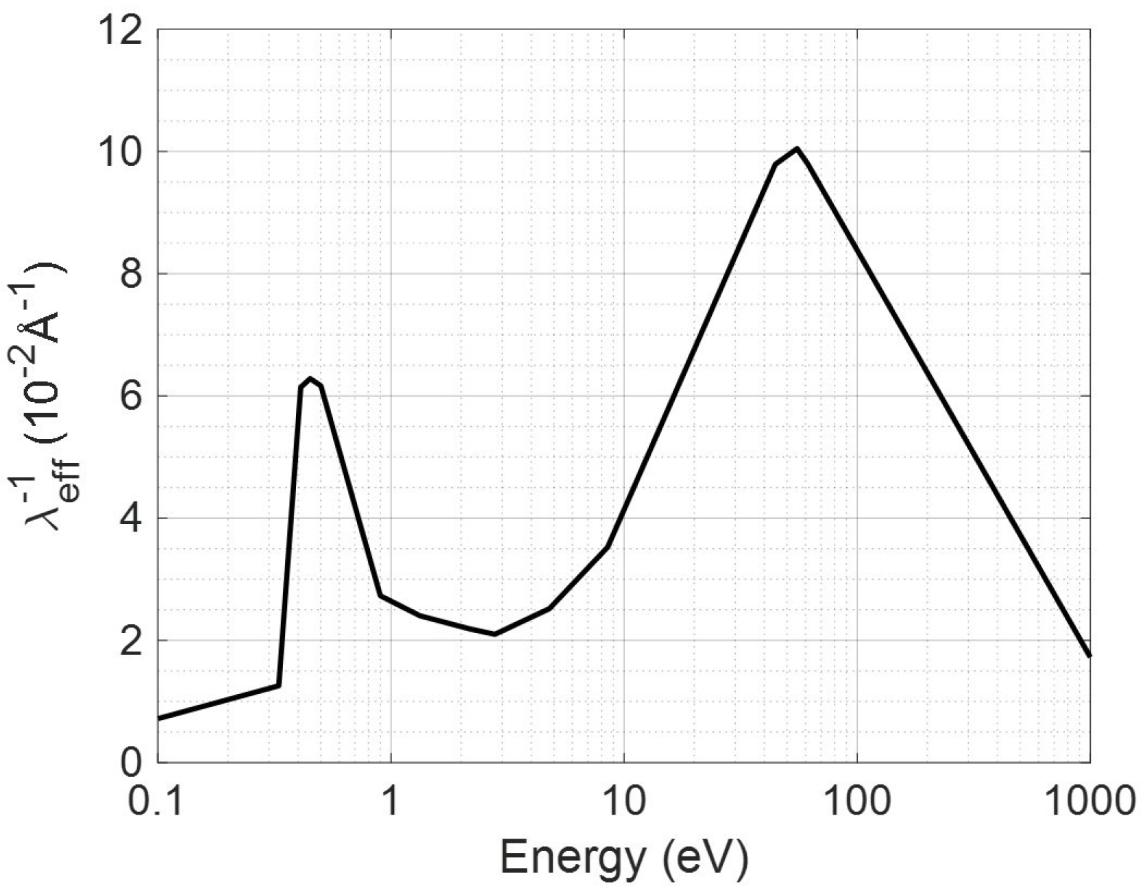
Figure 1. Energy dependence of reciprocal effective scattering length λ e f f 1 , taken from experiments and models in the range from 0.1 to 1000 eV [11,16].
Energies 17 03016 g001
Figure 2. Experimental setup for breakdown test. (a) Electrode arrangement, (b) experimental setup, (c) electrical layout of the experimental setup.
Energies 17 03016 g002
Figure 3. (a) Electrode configuration, (b) highlight of the HV electrode contour.
Energies 17 03016 g003
Figure 4. Surface partial discharge inception field (PDIE) obtained by the match of simulated tangential electric field profile maximum with the PD inception field model (1), at 0.7 kV for specimen A-0: PDIV = 0.7 kV. l1 and l2 are the distance values at which Ei = 0.9 Emax, Equation (2).
Energies 17 03016 g004
Figure 5. Electrical layout of the experimental setup for PDIV and surface erosion test.
Energies 17 03016 g005
Figure 6. Breakdown strength vs. thickness according to the model of Equation (3), applied to all tested materials and BV results of Table 3.
Energies 17 03016 g006
Figure 7. Comparison of the breakdown voltage of all tested materials referred to the same thickness (0.2 mm) based on model of Equation (3).
Energies 17 03016 g007
Figure 8. Comparison of the PDIV for all tested materials (along with mean thickness d).
Energies 17 03016 g008
Figure 9. PD patterns for the base material Polyphenylsulfone (PPSU) specimen A-0, at the start of aging (erosion) at 3PDIV. (a) The global phase-resolved PD (PRPD) pattern, (b) typical PD pulse, (c) separation (PCA) map with clustering, and (d) identification of the type of PD with likelihood of 90% surface and 10% internal.
Energies 17 03016 g009
Figure 10. PD patterns for the neat material Polyphenylsulfone (PPSU) specimen A-0, after 8 h of aging (erosion) at 3PDIV. (a) The global phase-resolved PD (PRPD) pattern, (b) typical PD pulse, (c) separation (PCA) map with clustering, and (d) identification of the type of PD with likelihood of 30% surface and 70% internal.
Energies 17 03016 g010
Figure 11. PD patterns for specimen D-14-m, at the beginning of aging (erosion) at 3PDIV. (a) The global phase-resolved PD (PRPD) pattern, (b) typical PD pulse, (c) separation (PCA) map with clustering, and (d) identification of the type of PD with likelihood of being 100% surface discharge.
Energies 17 03016 g011
Figure 12. PD patterns for material sample D-14-m, after 8 h of aging (erosion) at 3PDIV. (a) The global phase-resolved PD (PRPD) pattern, (b) typical PD pulse, (c) separation (PCA) map with clustering, and (d) identification of the type of PD with likelihood of 70% surface and 30% internal.
Energies 17 03016 g012
Figure 13. Image of pitting formation (optical microscope, magnification 20×) in specimen B-1-n, (a) at the beginning of aging, (b) after 2 h of aging, and (c) before breakdown.
Energies 17 03016 g013
Figure 14. Identification likelihood of surface PD (percentage) as a function of aging time. Experimental points (with 95% confidence intervals) and best fitting line for the neat specimen A-0.
Energies 17 03016 g014
Figure 15. Time trend of identification likelihood (percentage) for surface discharge for all tested materials (after linear fitting).
Energies 17 03016 g015
Figure 16. Summary of erosion test results (mean values), based on surface roughness measurements.
Energies 17 03016 g016
Figure 17. Percentage increase in surface roughness measured at time 0 h, 3 h, 5 h, 7 h, and 8 h during aging, for each tested material.
Energies 17 03016 g017
Figure 18. Example of correlation plot for percentage increase in surface roughness and likelihood of surface discharge (percentage) at different aging times for specimen A-0, with linear fitting.
Energies 17 03016 g018
Figure 19. Behavior of mean cumulative extrinsic stress (in relative value to unaged specimens) as a function of aging time for all tested materials.
Energies 17 03016 g019
Figure 20. (a) Example of cumulative extrinsic stress (relative to unaged specimen) with the likelihood of surface discharge (percentage) at different aging times for specimen A-0 with linear fitting; (b) Correlation coefficient (CC) values for all tested materials.
Energies 17 03016 g020
Table 1. Tested PPSU materials and thermal conductivity (m = microfiller, n = nanofiller).
Material TypeTested Specimen (Name)Thermal Conductivity (W/m·K)
Virgin Polyphenysulfone A-0 0.267
Polyphenylsulfone with ~1 wt% nanoBNB-1 n0.246
Plyphenylsulfone with ~6.1 wt% micro + nanoBNC-6.1 m+n0.323
Polyphenylsulfone with ~14 wt% micro BN D-14 m 0.396
Table 2. Dielectric constant, theoretical PD inception field (PDIE) and voltage (PDIV) values for test specimens.
Specimen TypeDielectric ConstantTheoretical PDIE (kV/mm)Theoretical PDIV (kV)
A-02.931.90.7
B-1 n3.392.00.8
C-6.1 m+n3.632.21.0
D-14 m3.682.20.9
KAPTON CR3.403.30.5
Table 3. Experimental results for breakdown voltage, breakdown strength, and PDIV (mean values).
Specimen TypeBreakdown Voltage (BV) (Mean)Thickness
(Min–Max)
Thickness at Breakdown PointBreakdown Strength (BS) at Breakdown Point (Mean)Dielectric Constant
at 64.2 Hz
PDIV
(Mean)
A-0 6.2 kV 0.06–0.2 mm 0.09 mm 68.8 kV/mm 2.93 0.7 kV
B-1 n 11.1 kV 0.13–0.26 mm 0.14 mm 79.2 kV/mm 3.39 0.8 kV
C-6.1 m+n15.2 kV0.14–0.3 mm0.15 mm101.3 kV/mm3.631.1 kV
D-14 m 13.1 kV 0.1–0.28 mm 0.12 mm 109.1 kV/mm 3.68 1 kV
KAPTON CR9.1 kV0.05 mm0.05 mm182 kV/mm3.400.5 kV
Disclaimer/Publisher’s Note: The statements, opinions and data contained in all publications are solely those of the individual author(s) and contributor(s) and not of MDPI and/or the editor(s). MDPI and/or the editor(s) disclaim responsibility for any injury to people or property resulting from any ideas, methods, instructions or products referred to in the content.