Article

Multi-Terminal GaInP/GaInAs/Ge Solar Cells for Subcells Characterization

1
Laboratoire Nanotechnologies Nanosystèmes (LN2)-CNRS UMI-3463, Université de Sherbrooke, Sherbrooke, QC J1K 0A5, Canada
2
Institut Interdisciplinaire d’Innovation Technologique (3IT), Université de Sherbrooke, Sherbrooke, QC J1K 0A5, Canada
*
Author to whom correspondence should be addressed.
Energies 2024, 17(11), 2538; https://doi.org/10.3390/en17112538
Submission received: 30 March 2024 / Revised: 10 May 2024 / Accepted: 14 May 2024 / Published: 24 May 2024

Abstract

:
Improvement of triple-junction (3J) III-V/Ge solar cells efficiency is hindered by the low current produced by the top and middle cells relative to the bottom cell (Ge). This can be explained by the difficulty of characterizing, on an individual basis, the subcells. We investigate the fabrication process of multi-terminal multi-junction solar cells (MTMJSC) and its potential as a promising architecture to independently characterize subcells of multi-junction solar cells. Here, we study monolithic triple-junction solar cells, with an InGaP top cell, an InGaAs middle cell and a Ge bottom cell interconnected by tunnel junctions. We demonstrate a fabrication process for MTMJSC on commercial wafers for characterization applications purposes. I-V measurements, under illumination, of two-terminals and MTMJSC were compared to validate that the MTMJSC fabrication process does not degrade the cells’ performance. The dark current of each subcell was also measured and an ideal-diode model used to determine the subcells electrical parameters. The results suggest a method to measure the relative absorption and the opto-electrical couplings between the subcells unambiguously, through EQE and electroluminescence measurements, based on basic micro-fabrication processes.

1. Introduction

Multijunction semiconductor photovoltaic cells are used for various commercial applications, such as solar triple-junction (3J) III-V/Ge cells, spatial or concentrated photovoltaics (CPV) applications [1,2,3], and optical power converters [4]. Triple-junction (3J) III-V/Ge solar cells reach efficiencies as high as 31.7% (at AM1.5G) [5,6]; however, 3J solar cells are far below their theoretical efficiencies of 50.7% (AM1.5G) [7]. One can mainly explain this room for improvement by the low short-circuit current densities (Jsc) produced by the top and the middle junction compared to the Ge bottom cell, these subcells being connected in series by tunnel junctions. This is why continuous improvement of these stacks relies on the optimization of the external quantum efficiency (EQE) and the bandgap of each subcell. The monolithic integration of multi-junction solar cells may imply subcells to be both optically and electrically coupled [8]. However, due to the complex stacking involved in this type of technology, characterization of two-terminals (2T) solar cells is rendered difficult. The main method employed to measure EQE, based on variation of light and voltage bias [9,10,11], requires a complex procedure to minimize a measurement artifact [8].
MTMJSC devices enable contacting of electrical subcells on an individual basis. These devices could allow for unambiguous measurements of each multi-junction subcell Jsc and J-V characteristics under working conditions [12].
In this article, we introduce a comprehensive process for the fabrication of InGaP/InGaAs/Ge MTMJSC for characterization purposes. The electric contacts are taken on the front side, on the top of each tunnel junction, and on the back side. We first describe the selective etching steps on which the process is based. We then show that the electrical properties obtained for these cells are comparable to those of two-terminal cells from the same commercial wafer, using a standard process [13]. We extracted the short-circuit current (Jsc), series resistance (Rs), shunt resistance (Rp), and the ideality factor (n) considering a 1-diode model from current density–voltage (J-V) characterization. Finally, EQE and electroluminescence (EL) were carried out on our samples to determine the impact of both electrical [9,10,14] and optical couplings [15].

2. Materials and Methods

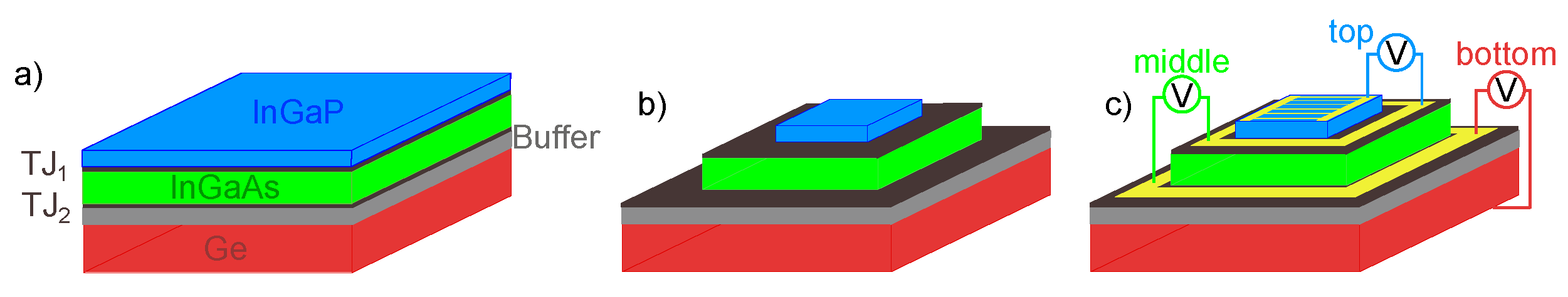
2.1. Device Fabrication

2.1.1. Process Flow

Figure 1 presents the simplified micro-fabrication process of triple-junction (3J) MTMJSC where the InGaP (top cell), InGaAs (middle cell) and the Ge (bottom cell) are shown in blue, green and red, respectively. The GaAs buffer layer between the Ge and the III-V are displayed in grey in Figure 1. First, wet etching processes are used to define mesas. We used a combination of HCl:H3PO4, H2SO4:H2O2:H2O and H2O2 chemical solutions. Then, metallic stacks were deposited to contact the top contact layer, the tunnel junctions (TJ1 and TJ2) and the Ge substrate. The final cells were 2.2 × 2.2 mm2, 2.6 × 2.6 mm2 and 3 × 3 mm2 for the top (TC), middle (MC) and bottom cell (BC), respectively. The fact that the TC, for which we expected a lower Jsc, had a smaller dimension is not an issue for our applications, as we are not looking for an optimal current match with this design. We plan to use EQE to study the current densities that should not be affected by cell size.

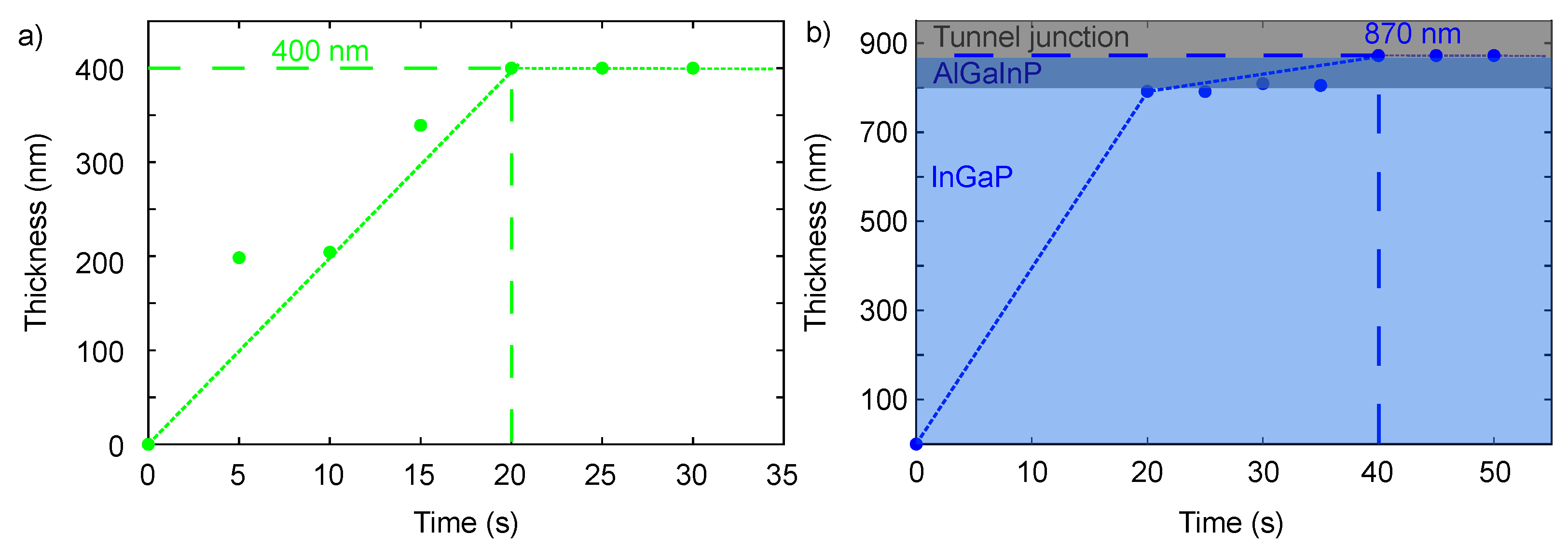
2.1.2. Selective Etching

Development of selective etching is a prerequisite for the fabrication of MTMJSC. This process is critical as it would allow to stop the etching at the targeted layer, i.e., at the top of the p-type of TJ1 and TJ2. To do so, the etching times need to be optimized to reduce possible under-etch. The fabrication process that we present hereafter (see Figure 1) is based on three chemical wet etching, selected by their selectivity. We focus in this section on the development and characterization of two wet etching solutions. The first etching process uses H2SO4:H2O2:H2O (1:10:20) (process 1) to etch GaAs-containing layers (GaAs, InGaAs and AlGaAs) selectively to P-containing layers (InGaP and AlInGaP), which are etched using a second etching process (process 2) based on HCl:H3PO4 (4:1). To avoid the formation of bubbles during the HCl:H3PO4 (1:4) etching process (process 2), the ratio between HCl and H3PO4 was optimized and the etching was performed in an ultrasonic bath [16].
To confirm the selectivity of the wet etching processes [17], we performed etching on blanket samples with various times. Cross-sectional SEM images were employed to measure the evolution in thicknesses of the layers being etched. Figure 2a,b show, respectively, the evolution of the top cell contact layer (GaAs) and the top subcell absorber layer (InGaP) thicknesses as a function of the exposure time in the etching solutions.
The cap layer (GaAs) etched during process 1 (Figure 2a) was measured to be 400 nm. After 20 s we observed a change in color. Then, cross-section measurements confirmed that the targeted 400 nm of the top contact layer was entirely etched. The selectivity was otherwise confirmed by the fact that the thickness no longer evolved after 20 s. The underneath P-containing window layer (n-InGaP window layer of the top cell) acted as an etch stop layer. The evolution of the InGaP layer thickness during exposure to solution 2 is shown in Figure 2b. The 870 nm of the top cell was etched within 40 s. It was observed that the first 850 nm was etched within the first 20 s, with a change in color. This first step is attributed to the InGaP etching. Then, the last 20 nm were etched in the next 20 s with a second change in color, corresponding to the AlGaInP (p-AlGaInP BSF layer of the top cell). We successfully etched the targeted 870 nm of the top cell; the underneath GaAs-containing tunnel junction was the etch stop. Using a similar methodology, we estimated the etching times required for the wet etching of the different III-V layers. Finally, when all the III-V layers had been etched, the Ge bottom cell was etched for 40 min at 50 °C in H2O2 (process 3). The etching times and chemical solutions used are summarized in Table 1.
By etching the different layers successively, a 3-stage mesa with pedestals stopping at each tunnel junction was fabricated (as described in Figure 1b).

2.2. Ohmic Contacts

Thereafter, we deposited metal contacts and the ohmic behavior was assessed. Transmission line method (TLM) measurements were performed to characterize the ohmic contacts. The following metal stacks were used to obtain ohmic contacts and we evaluated the specific contact resistivity through TLM measurement on planary etched samples: Pt/Ti/Au for n-AlGaAs layer ( ρ c = 3.8 ± 0.9 × 10 4 Ohm·cm2) and Cu/Pt/Ti/Pt/Au ( ρ c = 1.9 ± 1 × 10 4 Ohm·cm2) [18]. The front contact grid lines were fabricated by a standard Ni/Ge/Au/Ni/Au evaporation and lift-off [19]. For the base contact on the Ge substrate, the standard metallization consisted of an ohmic contact made of Ni/Au [19]. Finally, MTMJSC were bound to a PCB receiver and wire bonded to obtain the final device. This last step was performed to adapt the devices to all the characterization tools presented below.

2.3. Reference Cells

In the next section, our MTMJSC are compared to a 2.2 × 2.2 mm2 two terminals reference cell, fabricated using the same epitaxy, following the fabrication process developed in [13] with a plasma mesa etching and no anti-reflection coating.

2.4. Characterization

2.4.1. External Quantum Efficiency

EQE measurements were performed using a QEX10 (PV Measurements, Point Roberts, WA, USA) tool, which was calibrated over the 300–1750 nm range based on Si and Ge reference cells. A squared aperture of 1 mm2 was used to ensure that the spot size was smaller than the sample cell size. Measurements of the MTMJSC subcells were first performed with no applied voltages on the subcells. Then, the reference cell was measured based on the procedure presented in [9], where light biases, together with a voltage bias, needed to be refined to ensure that the cell under investigation was in short-circuit conditions [9,10,20]. However, despite fine tuning of the biases, a measurement artifact was observed and corrected using the method developed in [10]. During the “classic” EQE measurement of the BC, the unmeasured cells were under a light bias and, therefore, at a certain non-zero VMC and VTC potential. Due to electrical coupling and the low Rp of the BC cell, a current was generated by the measurement method.

2.4.2. Electroluminescence

We performed electroluminescence (EL) measurements on MTMJSC using a home-made EL system. This system presents a ×5 objective lens (Mitutoyo Plan Apochromat Objective, 436–656 nm, 0.14 NA, 34 mm WD) to visualize and collect the light from the cell. An MT-40 tube lens was then used to focus the light of the Si-camera (DCC1545M-Thorlabs) with all the filters removed. A Keithley 2601A was used to perform I-V measurements on the Ge subcell, together with a Keithley 2461A for the subcell polarization. Finally, a short-pass filter (FESH0750) with a cut-off wavelength of 750 nm was used to collect only the TC EL. Regarding the filtering of the MC EL, a short-pass filter (FESH1000) with a cut-off wavelength of 1000 nm was coupled to a long-pass filter (FELH0750) with a cut-off wavelength of 750 nm. The absolute calibration was not performed for this system, and so the results are shown in cts·s−1. Regarding the optical coupling measurements between the MC and the BC, the same voltage reference was imposed (as depicted in the simplified electric diagram in the inset in Figure 5).

3. Results and Discussion

In this section, we first compare MTMJSC with a reference cell and demonstrate the relevance of MTMJSC for investigation of the subcells’ optical and/or electrical coupling.

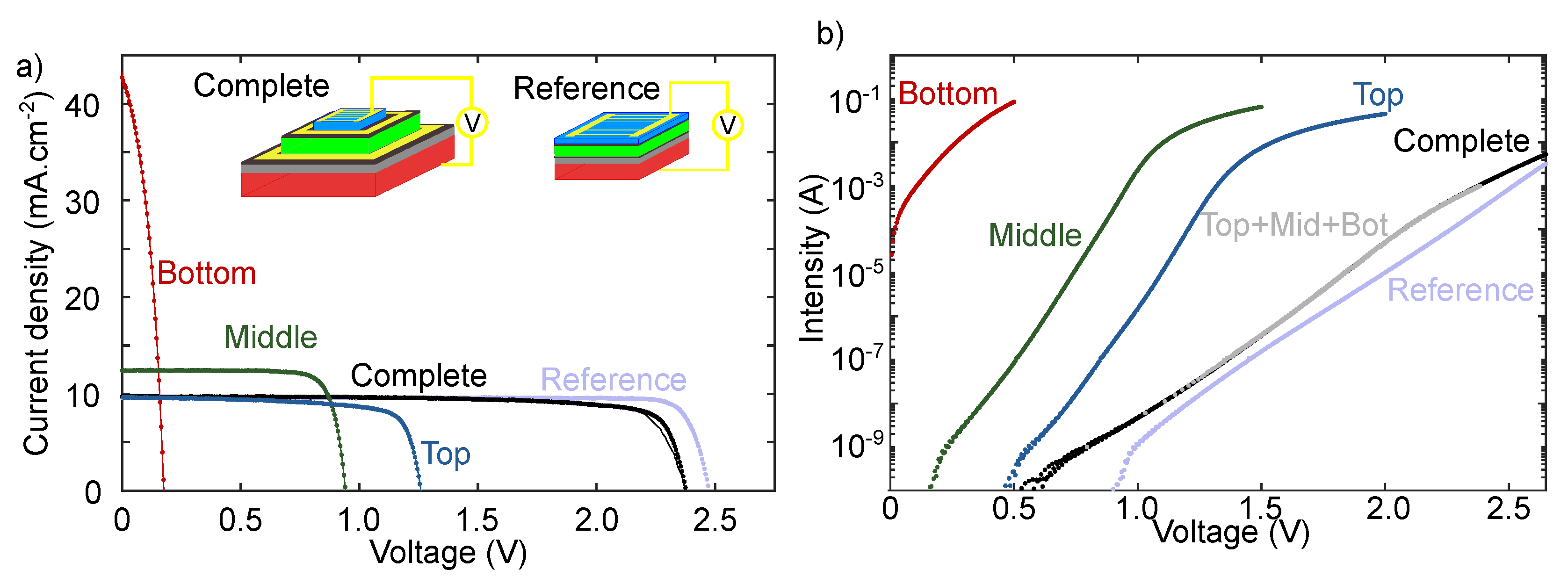
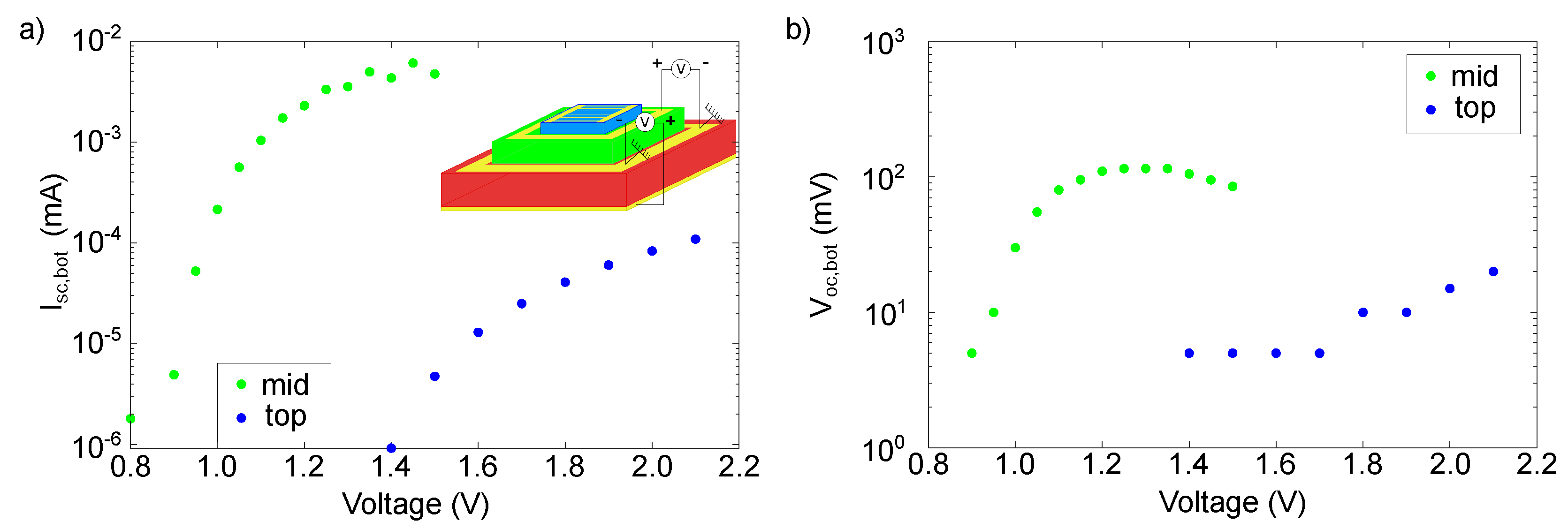
3.1. I-V Measurements

The reference (ref) and MTMJSC cells and subcells were characterized by current–voltage (I-V) measurements 1-sun conditions (Figure 3a) and under dark (Figure 3b). I-V measurements of each individual subcell were performed under open circuit conditions of the other two subcells. A 1-sun illumination condition (AM1.5D) was calibrated with a 2T InGaP/InGaAs/Ge commercial solar cell with an active cell area of 9.16 mm2. The 1-sun I-V curves of each subcell were then fitted with a one-diode model and plotted in Figure 3 to determine the electrical parameters on an individual basis. The results of the fits (J0, n, Rp and Rs) are summarized in Table 2.
Figure 3a shows that the MTMJSC and the reference cell possess similar I-V characteristics except for the Voc values. This lower value can be explained by a higher saturation current, as observed in Figure 3b. The lower Voc relative to the standard cell can be attributed to higher surface recombination on the edges of each subcell introduced by the mesas etching steps and a higher surface/perimeter ratio [21]. The similar I-V characteristics confirm that the final MTMJSC device possesses comparable electronic properties to a reference cell when measured between the emitter of the top subcell and the base of the bottom subcell (see “complete cell” scheme in Figure 3a). Figure 3b shows that each final subcell possesses diode-like behavior. The electrical parameters determined from the 1-diode model confirmed a low parallel resistance of tens of ohms for the Ge BC. To confirm the consistency of the results, the subcells voltage at a given current was added and compared to the 2-terminals MTMJSC complete cell in dark conditions (grey curve in Figure 3b). A very good agreement was observed. We then compared the results of the model to the final MTMJSC complete cell. We considered three diodes, defined by the electrical parameters summarized in Table 2, serially interconnected, and, as previously, we added the subcells voltage at a given current (gray continuous line in Figure 3a). The small discrepancy between the two curves is related to an overestimation of the series resistance due to the additional contact resistance inherent to the multi-terminal device. This result confirms that we can neglect the role played by tunnel junctions.
We infer the relevance of the fabrication process of MTMJSC as it reveals comparable electrical behavior to a reference cell. Furthermore, the electrical measurements suggest a low shunt resistance for the BC and that the 3J cell is top cell (TC)-limited.

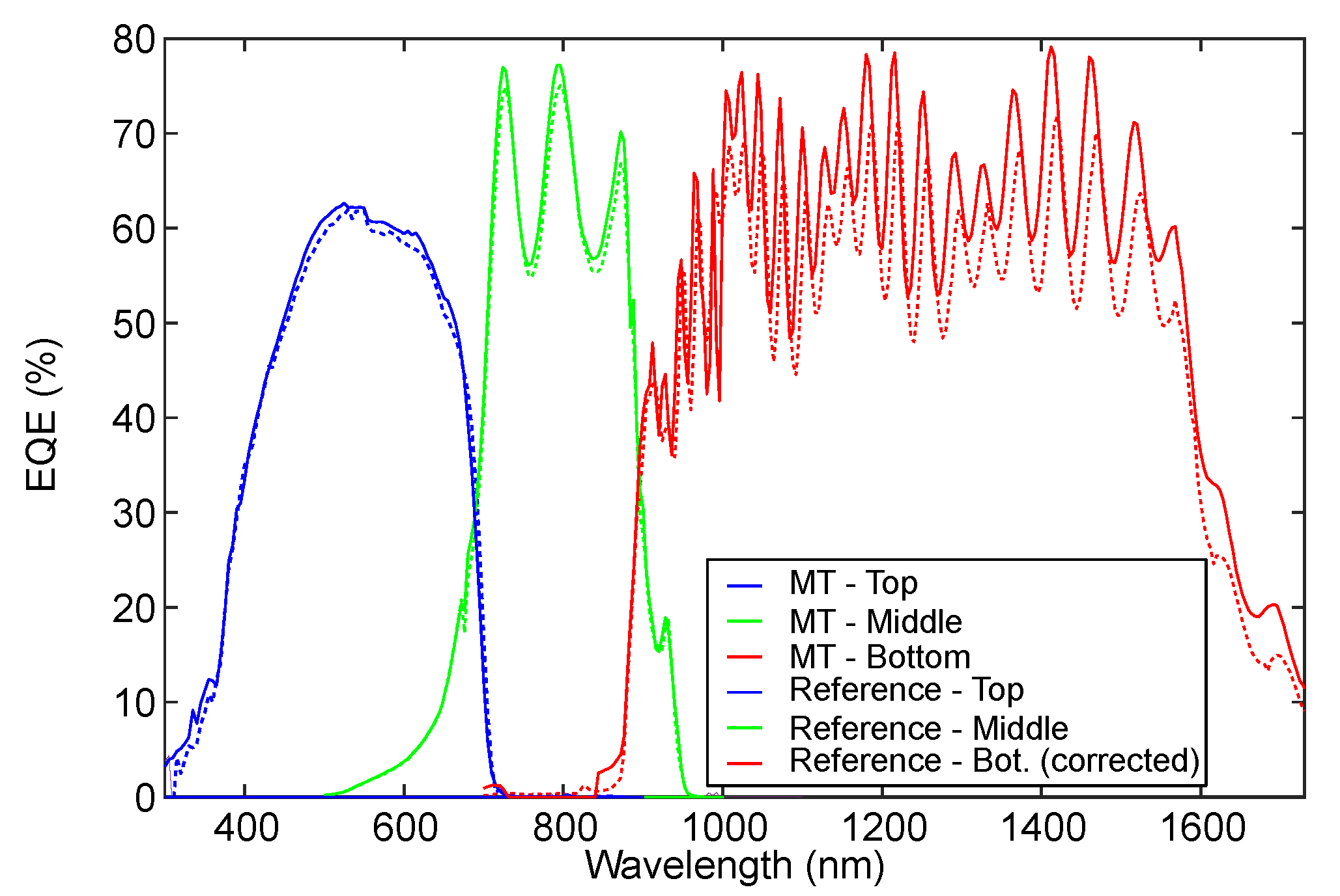
3.2. EQE Measurements

Figure 4 presents a comparison of the EQE measurements of the reference and MTMJSC cells performed with the light biases measurement method and the direct method, respectively. The comparison reveals that similar signals were measured for the TC and MC when comparing the two methods. Regarding the BC, a measurement artifact was observed and then corrected following the methods presented in [9], inducing a drop in the signal of the BC cell at 810 nm. This artifact was caused by an electrical and/or optical coupling between the bottom cell and the two other subcells. Our experimental results regarding the optimization of Vbias and light biases agree with simulations reported by Meusel et al. [9] when considering Rp = 50 ohm·cm2 (which is the same order of magnitude of the shunt resistance we determined previously (Table 2)). Nevertheless, even with optimal conditions (light and voltage biases), the artifact current corresponds to 1% of the bottom cell’s current. From these results, we can conclude that MTMJSC allows for a more straightforward EQE characterization of a multijunction stack in comparison to the light biases method. Indeed, direct measurement can be performed and no signal correction is required.

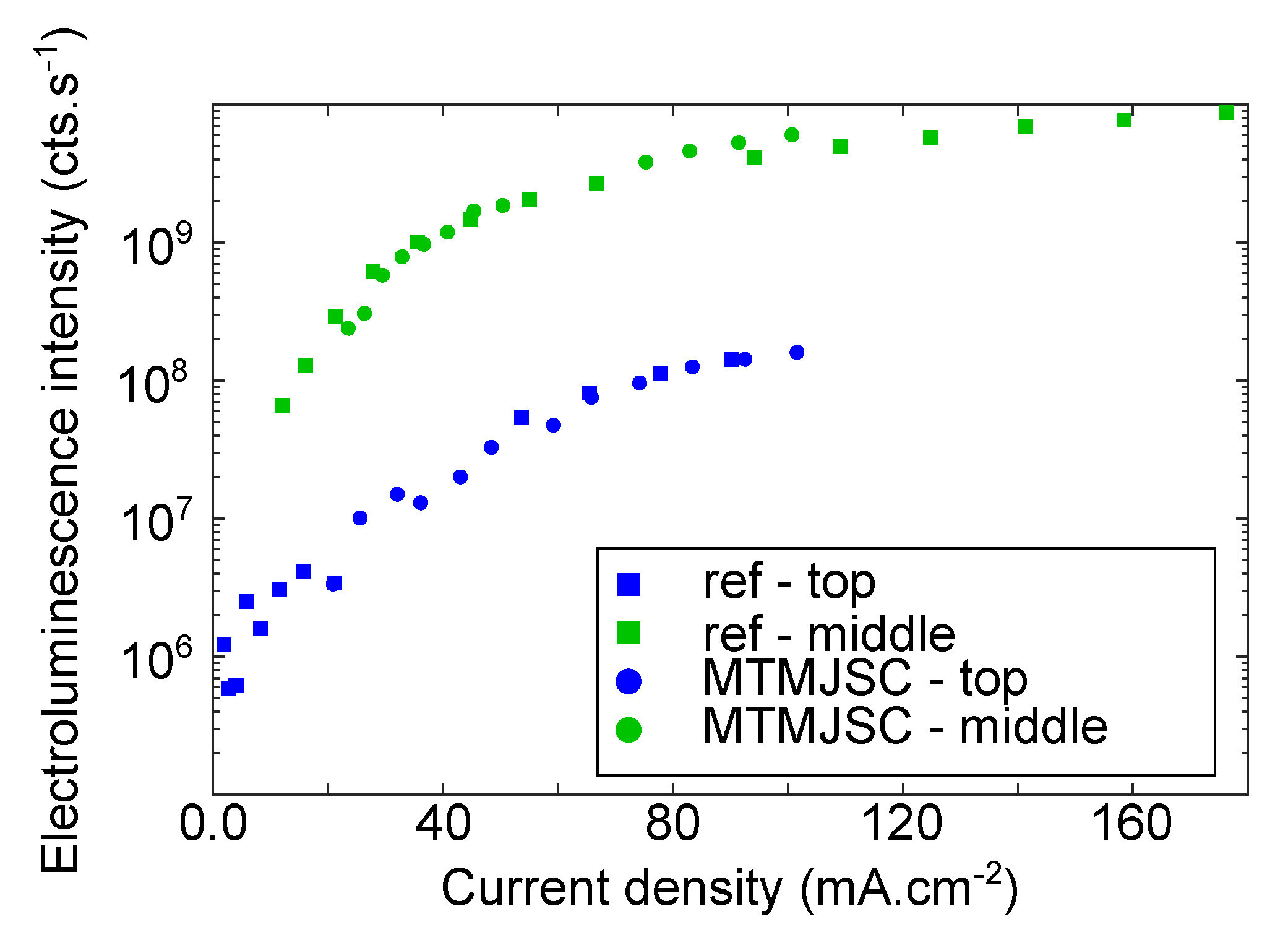
3.3. Electroluminescence Measurements

We observed previously the impact of the electrical coupling between the BC and the MC on EQE measurements. This highlights possible optical coupling between the light emitted by the TC and the MC and the BC. Based on MTMJSC, we can determine the light emitted by each subcell under working conditions as well as the current generated in the subcells underneath.
We performed I-V measurements where both the current density going through the cell and the EL intensity for each voltage were measured. Figure 5 presents the evolution of the EL intensity as a function of the current passing through the subcells. As we increase the applied voltage the current going through the subcells increases. Then, a part of this current generates an EL signal through radiative recombinations. We observe that for both the TC (blue) and the MC (green), the proportion of the current recombining radiatively decreases, as the slopes decrease as we increase the current density. This reduction in the radiative efficiency in high injection levels may be attributed to non-negligible Auger recombination. To compare the results between the reference cell and the MTMJSC, in Figure 5, we superimposed the EL intensities for both the reference cell (squares) and the MTMJSC (circles) as a function of the current density. We can observe that the data from both measurements match almost perfectly. Comparable tendencies in the evolution of the EL signal as a function of the current were observed by Roensch et al. [22] for a 2T cell.
Then, we measured the current generated in the BC from the EL coming from both the TC and the MC. To do so, we applied a voltage at the TC or MC, and we measured the I-V characteristics for the BC. From these I-V measurements, we determined the Jsc (Figure 6a) and Voc (Figure 6b) values as a function of the voltage applied on the TC or MC. An optical coupling could only be measured from a certain voltage, which is from 1.3 V for the coupling between the TC and the BC and 0.85 V for the coupling between the MC and the BC. We can observe in (Figure 6a) that by increasing the voltage applied on the TC (blue dots) or the MC (green dots), the photogenerated current in the BC increases. We can see that the BC open circuit voltage (Voc,bot(Vtop)) increases from 5 to 20 mV when the top cell voltage increases from 1.3 to 2.1V. Finally, Voc,bot(Vmid) starts increasing from 5 mV up to 100 mV before reaching a plateau and then decreases when Vmid exceeds 1.3V. No clear explanation for this phenomenon was found, but it seems to be activated above a certain voltage. The I-V curves measured for the Ge subcell were analyzed and no evolution in the shunt was observed. This confirms that we observed a different phenomenon than Li et al. [8]. Heating of the MC when operating in high injection levels, leading to an increase in the BC temperature, could explain such behavior.
Finally, from the I-V measured under 1-sun (Figure 3b), we can determine the maximal power point (mpp) for each subcell: Vmpp,top = 1.06 V and Vmpp,middle = 0.89 V. These voltages are below the lower limit from which we were able to measure an optical coupling. This suggests, from Figure 6a, that no optical coupling is expected between cells under working conditions.

4. Conclusions

In conclusion, we presented a fabrication process of an MTMJSC based on selective wet etching. First, the I-V comparison between a two-terminal reference cell and MTMJSC attests to the relevance of the fabrication of such devices to determine the electrical parameters of each subcell of a commercial wafer. We showed how MTMJSC solar cells allow for unambiguous characterization of triple-junction solar cells through EQE and EL measurements. Optical coupling between subcells was highlighted based on the use of EL measurements and suggests the absence of optical coupling under 1-sun working conditions. Finally, MTMJSC could also be used for calibration of characterization tools and implemented for continuous improvement of III-V multijunction solar cells.

Author Contributions

Conceptualization, T.B., M.D. and G.H.; methodology, T.B.; validation, T.B., F.A., C.J., S.M., A.T. and P.F.; formal analysis, T.B., F.A. and P.F.; investigation, T.B., F.A. and P.F.; resources, M.D., G.H. and V.A.; data curation, T.B.; writing—original draft preparation, T.B.; writing—review and editing, T.B., M.D., G.H., S.F. and A.J.; visualization, T.B.; supervision, M.D., M.V. and G.H.; project administration, M.D., G.H. and V.A.; funding acquisition, M.D., G.H. and V.A. All authors have read and agreed to the published version of the manuscript.

Funding

This research received no external funding.

Data Availability Statement

The data presented in this study are available on request from the corresponding author.

Acknowledgments

LN2 is a joint International Research Laboratory (IRL 3463) funded and co-operated by Université de Sherbrooke (Canada) and CNRS (France) as well as INSA Lyon, ECL, Université Grenoble Alpes (UGA) as well as the French national nanofabrication network RENATECH. The support from NSERC, Prompt and STACE through the MARS-CPV project is acknowledged.

Conflicts of Interest

The authors declare no conflicts of interest.

References

  1. Ejaz, A.; Babar, H.; Ali, H.M.; Jamil, F.; Mansoor Janjua, M.; Fattah, I.M.R.; Said, Z.; Li, C. Concentration photovoltaics as light harvesters: Outlook, recent progress, and challenges. Sustain. Energy Technol. Assess. 2021, 46, 101199. [Google Scholar]
  2. Baiju, A.; Yarema, M. Status and challenges of multi-junction solar cell technology. Front. Energy Res. 2022, 10, 971918. [Google Scholar] [CrossRef]
  3. Wiesenfarth, M.; Anton, I.; Bett, A.W. Challenges in the design of concentrator photovoltaic (CPV) modules to achieve highest efficiencies. App. Phys. Rev. 2018, 5, 041601. [Google Scholar] [CrossRef]
  4. Fafard, S.; Masson, D.P. Perspective on photovoltaic optical power converters. J. Appl. Phys. 2021, 130, 160901. [Google Scholar] [CrossRef]
  5. Green, M.A.; Dunlop, E.D.; Siefer, G.; Yoshita, M.; Kopidakis, N.; Bothe, K.; Hao, X. Solar cell efficiency tables (Version 61). Prog. Photovolt. Res. Appl. 2023, 31, 3–16. [Google Scholar] [CrossRef]
  6. Yamaguchi, M.; Dimroth, F.; Geisz, J.F.; Ekins-Daukes, N.J. Multi-junction solar cells paving the way for super high-efficiency. J. Appl. Phys. 2021, 129, 240901. [Google Scholar] [CrossRef]
  7. Almansouri, I.; Ho-Baillie, A.; Bremner, S.P.; Green, M.A. Supercharging Silicon Solar Cell Performance by Means of Multijunction Concept. IEEE J. Photovolt. 2015, 5, 968–976. [Google Scholar] [CrossRef]
  8. Li, J.-J.; Lim, S.H.; Allen, C.R.; Ding, D.; Zhang, Y.-H. Combined Effects of Shunt and Luminescence Coupling on External Quantum Efficiency Measurements of Multijunction Solar Cells. IEEE J. Photovolt. 2011, 1, 225–230. [Google Scholar] [CrossRef]
  9. Meusel, M.; Baur, C.; Létay, G.; Bett, A.W.; Warta, W.; Fernandez, E. Spectral Response Measurements of Monolithic GaInP/Ga(In)As/Ge Triple-junction Solar Cells: Measurement Artifacts and Their Explanation. Prog. Photovolt. 2003, 11, 499–514. [Google Scholar] [CrossRef]
  10. Siefer, G.; Baur, C.; Bett, A.W. External Quantum Efficiency Measurements of Germanium Bottom Subcells: Measurement Artifacts and Correction Procedures. In Proceedings of the 2010 35th IEEE Photovoltaic Specialists Conference, Honolulu, HI, USA, 20–25 June 2010; pp. 000704–000707. [Google Scholar]
  11. Fafard, S.; Valdivia, C.E.; Wallace, S.G. The “Fill-Factor Bias Measurement” for Advanced Triple-Junction Solar Cell Characterization and Quality Control. In Proceedings of the 8th International Conference on Concentrating Photovoltaics System: CPV-8, Toledo, Spain, 16–18 April 2012; pp. 118–121. [Google Scholar]
  12. Steiner, M.A.; Wanlass, M.W.; Carapella, J.J.; Duda, A.; Ward, J.S.; Moriarty, T.E.; Emery, K.A. A Monolithic Three-terminal GaInAsP/GaInAs Tandem Solar Cell. Prog. Photovolt. 2009, 17, 587–593. [Google Scholar] [CrossRef]
  13. Albert, P.; Jaouad, A.; Hamon, G.; Volatier, M.; Valdivia, C.E.; Deshayes, Y.; Hinzer, K.; Béchou, L.; Aimez, V.; Darnon, M. Miniaturization of InGaP/InGaAs/Ge Solar Cells for Micro-concentrator Photovoltaics. Prog. Photovolt. 2021, 29, 990–999. [Google Scholar] [CrossRef]
  14. Meusel, M.; Baur, C.; Siefer, G.; Dimroth, F.; Bett, A.W.; Warta, W. Characterization of Monolithic III–V Multi-Junction Solar Cells—Challenges and Application. Sol. Energ. Mat. Sol. C 2006, 90, 3268–3275. [Google Scholar] [CrossRef]
  15. Shu, G.W.; Lin, J.Y.; Jian, H.T.; Shen, J.L.; Wang, S.C.; Chou, C.L.; Chou, W.C.; Wu, C.H.; Chiu, C.H.; Kuo, H.C. Optical coupling from InGaAs subcell to InGaP subcell in InGaP/InGaAs/Ge multi-junction solar cells. Opt. Express. 2003, 21, S1. [Google Scholar] [CrossRef] [PubMed]
  16. Notten, P.H.L. The Etching of InP in HCl Solutions: A Chemical Mechanism. J. Electrochem. Soc. 1984, 131, 2641–2644. [Google Scholar] [CrossRef]
  17. Clawson, A.R. Guide to References on III V Semiconductor Chemical Etching. Mater. Sci. Eng. 2001, 31, 1–438. [Google Scholar] [CrossRef]
  18. Ayari, F.; Moreau, S.; de Lafontaine, M.; Turala, A.; Bidaud, T.; Hamon, G.; Volatier, M.; Aimez, V.; Jaouad, A.; Darnon, M. Multi-Terminal Three-Junction Solar Cells for Sub-Cells Characterization. In Proceedings of the 18th Conference on Concentrated PhotoVoltaics System, Miyazaki, Japan, 25–27 April 2022. [Google Scholar]
  19. De Lafontaine, M.; Pargon, E.; Petit-Etienne, C.; Gay, G.; Jaouad, A.; Gour, M.-J.; Volatier, M.; Fafard, S.; Aimez, V.; Darnon, M. Influence of Plasma Process on III-V/Ge Multijunction Solar Cell via Etching. Sol. Energ. Mat. Sol. C 2019, 195, 49–54. [Google Scholar] [CrossRef]
  20. Burdick, J.; Glatfelter, T. Spectral Response and I–V Measurements of Tandem Amorphous-Silicon Alloy Solar Cells. Sol. Cells 1986, 18, 301–314. [Google Scholar] [CrossRef]
  21. De Lafontaine, M.; Ayari, F.; Pargon, E.; Gay, G.; Petit-Etienne, C.; Turala, A.; Hamon, G.; Jaouad, A.; Volatier, M.; Fafard, S.; et al. Multijunction Solar Cell Mesa Isolation: Correlation between Process, Morphology and Cell Performance. Sol. Energ. Mat. Sol. C 2022, 239, 111643. [Google Scholar] [CrossRef]
  22. Roensch, S.; Hoheisel, R.; Dimroth, F.; Bett, A.W. Subcell I-V Characteristic Analysis of GaInP/GaInAs/Ge Solar Cells Using Electroluminescence Measurements. Appl. Phys. Lett. 2011, 98, 251113. [Google Scholar] [CrossRef]
Figure 1. Main steps in the MTMJSC fabrication process flow from (a) a triple-junction: InGaP (blue)/InGaAs (green)/Ge (red) wafer where tunnel junction 1 and 2 and the GaAs buffer layer (gray) are also displayed. Process flow steps are separated between, first (b) wet etching and (c) metal contact deposition.
Energies 17 02538 g001
Figure 2. Evolution of the etched thickness as a function of the etching time for planar wet etching of (a) GaAs layer in H2SO4:H2O2:H2O (1:10:20) of a and (b) P-containing layer (AlGaInP, InGaP, AlInP) in HCl:H3PO4 (4:1). The dotted lines serve as guides to the eye to highlight both the etching trend and final etched thicknesses and times. Thicknesses were determined through cross-sectional SEM imaging.
Energies 17 02538 g002
Figure 3. (a) 1-sun I-V curve of reference (purple), complete (black), top (blue), middle (green), bottom (red) and top + middle + bottom serially interconnected (gray) (b) I-V curve of reference (purple), complete (dark), top (blue), middle (green), bottom (red) and top+middle+bottom serially interconnected (gray).
Energies 17 02538 g003
Figure 4. EQE measurements performed on reference cell 2-terminals based on the light bias method (continuous lines) and an MTMJSC measured with a direct method (dashed lines). A signal correction was applied to the reference cell BC signal to reduce the artifact.
Energies 17 02538 g004
Figure 5. Electroluminescence intensity emitted by the top (blue) and the middle (green) cell measured on 2T reference cell (squares) and MTMJSC cell (circles).
Energies 17 02538 g005
Figure 6. (a) Evolution of the Isc bottom cell as a function of the applied voltage on the top (blue dots) and the middle cell (green dots). Inset presents a scheme of the experimental setup for the optical coupling measurements between the middle (green) and the bottom (red) solar subcells. (b) Evolution of the Voc induced in the BC as a function of the applied voltage on the top Voc,top (blue dots) and the middle cell Voc,mid (green dots).
Energies 17 02538 g006
Table 1. Summary table of the thicknesses and etching times applied for the MTMJSC fabrication process.
LayerThickness
nm
Etching
Process
Etching
Time (s)
Cap layer
(GaAs)
400(1)25
Top cell
window/absorber/BSF
(AlInP/InGaP/AlGaInP)
870(2)40
Tunnel junction 1
(p++)
AlGaAs
50(1)3
Tunnel junction 2 (n++)50(2)3
(InGaInP)
Middle cell *
Window
(InGaP)
(2)
Middle Cell
Absorber
(InGaAs)
3700(1)240
Middle Cell
BSF
(InGaP)
150(2)7
Tunnel junction 2 (p++)
(GaAs)
50(1)
Tunnel junction 2 (n++)
(GaAs)
50(1)240
Buffer
(InGaAs)
2900(1)
Bottom cell *
(Ge)
(3)2400
* No precise measurements of the thickness were performed for this layer.
Table 2. Electrical parameters extracted from I-V measurements under 1-sun illumination based on 1-diode model fits (continuous lines in Figure 3).
SubcellJ0
(mA·cm−2)
nRs
(ohm·cm−2)
Rp
(ohm·cm−2)
top6.7 × 10−111.91.9 × 10−5103
middle1.8 × 10−81.83.9 × 10−5104
bottom12.01 × 10−1101
Disclaimer/Publisher’s Note: The statements, opinions and data contained in all publications are solely those of the individual author(s) and contributor(s) and not of MDPI and/or the editor(s). MDPI and/or the editor(s) disclaim responsibility for any injury to people or property resulting from any ideas, methods, instructions or products referred to in the content.

