Article

A New Double-Switch SEPIC-Buck Topology for Renewable Energy Applications

1
Energy Engineering Department, Engineering Technology Faculty, Zarqa University, Zarqa 13110, Jordan
2
Cyber Security Department, Information Technology Faculty, Isra University, Amman 11622, Jordan
3
Electrical (Communications and Electronics) Engineering Department, Engineering Faculty, Isra University, Amman 11622, Jordan
*
Author to whom correspondence should be addressed.
Energies 2024, 17(1), 238; https://doi.org/10.3390/en17010238
Submission received: 15 September 2023 / Revised: 27 October 2023 / Accepted: 10 November 2023 / Published: 2 January 2024
(This article belongs to the Special Issue Advanced DC-DC Power Converters and Switching Converters II)

Abstract

:
In addition to their conventional use in electric motor drives, DC-DC converters have a variety of other uses, such as energy storage, energy conversion, cyber security systems, uninterruptible power supplies, and renewable energy systems. An innovative DC-DC converter is suggested in this article. Designing a new, high-gain DC-DC converter scheme known as a double-switch SEPIC-buck converter (DSSB) is possible after making some adjustments to the SEPIC converter that is currently known in accordance with accepted techniques. The output voltage magnitude of the proposed converter is either larger than or less than the input voltage magnitude and is the same sign as the input voltage. According to the theoretical and analytical study that has been supported by the real-world application, high voltage gain, low switching stress, and low inductor current ripple are the main characteristics of the proposed DSSB converter. The related small-signal model was also used to build the closed-loop system. The frequency response and output voltage behavior were investigated when the input source voltage abruptly changed as a step function. Based on the comparison study with other DC-DC converters, the DSSB converter outperforms currently known DC-DC converters such as Buck, SEPIC, Boost, Buck-Boost, and other SEPIC converter topologies in terms of voltage gain, harmonic content, normalized current ripple, dynamic performance, and efficiency. Additionally, the frequency response and control of the proposed converter using an alternate current (AC), small-signal, analysis-based, current-mode control technique are both provided. Thus, the DSSB is regarded as safe in overcurrent situations because of the small-signal analysis with the current control strategy. As a result of the verification of the proposed control technique, the resistance to changes in the DSSB parameters, improved dynamic performance, and higher control accuracy are further advantages of current-mode control based on small-signal analysis over other control approaches (PI controllers). Finally, the experimental and simulation results from Simplorer 7 and MATLAB/Simulink are used to validate the findings of the analytical and comparative investigation.

1. Introduction

Power electronic converters are essential in many industrial applications, as they produce a DC voltage supply stabilized to a certain value from a DC voltage supply. These converters usually offer an adequate size, weight, and volume for low-, medium-a, and high-power operations ranging from tens of watts to hundreds of kW [1,2].
Power electronic converters are also utilized to get the proper stepping-up/stepping-down voltages to utilize combined renewable energy resources for intelligent microgrid and power system conversions as efficiently as feasible [3,4].
Many industrial applications require the use of high voltage gain DC-DC converters, such as vehicle headlamps, fuel cells, solar cells, and battery backup systems for uninterruptible power sources, autonomous and intelligent residential sector electricity storage systems, telecommunication power supplies, cyber security systems, and voltage regulators for energy conversion systems [5,6].
Traditional DC-DC converters such as bucks, boosts, and buck-boosts are the pre-select when switching to step-up/step-down voltage regulation, respectively, mainly due to their simple structures and their low number of electronic/electrical components. However, these converters’ duty cycles (switching ratio) must be at their highest levels to provide a little higher voltage gain, which is insufficient to meet the industrial demands of the above-mentioned applications [7].
Therefore, the wide conversion range DC-DC converter has recently been the subject of much research in power electronics, leading to the visualization of many structures with deep-rooted advantages and disadvantages in terms of switching duty ratios, the number of components, and the associated voltage stress of their semiconductor devices. In addition, most of these studies focus on the high-voltage boost conversion process using different methods such as cascade and parallel stages, coupled inductors (inductors), parallel coupled capacitors, and so on [1,2,3,4,5,6,7,8]. Although there are many research articles on DC/DC converters, there are still many related problems that need to be solved, such as maximum power point tracking, efficiency, voltage gain, current ripple minimization, buck-boost operation regime, quadratic boost, and buck converters [8,9].
For instance, the decrease of current ripple and the voltage stress on the converter switches are studied for an interleaved three-phase boost converter with magnetically coupled inductors that is utilized to power a brushless DC motor fed by solar energy at its highest power point. As the study demonstrates, the suggested converter system has demonstrated advantages over a noncoupled three-phase interleaved boost converter, including low ripple content on both the load and supply sides, improved efficiency, and reduced switch stress Vinay Kumar et al. [10].
Al Attar H. et al. [11], also studied the current ripple reduction, reduced voltage stress, and improved efficiency for bidirectional electric vehicle (EV) chargers. As demonstrated by Al Attar H et. al., 2023, bidirectional DC-DC converters can be effectively employed for applications needing high power density, such as bidirectional electric vehicle (EV) chargers. Other control systems combine different modulation techniques with a small- or large-signal model. In this industrial application, a DC-DC converter couples an AC-DC converter, a high-voltage battery pack, and a DC bus link. The use of DC-DC converters with bidirectional electric vehicle (EV) chargers reduces voltage stress, increases efficiency, and reduces the current ripple, according to Al Attar H et al. [11].
According to Solis-Rodriguez et. al. [12], the Low Energy Storage Quadratic Boost Converter (LES-QBC) with the Particle Swarm Optimization (PSO) technique offers a lower Output Voltage Ripple (OVR) than a standard quadratic boost converter with capacitors of the same characteristics. The Particle Swarm Optimization (PSO) technique was used to investigate the optimization of a recently developed DC-DC converter capacitor selection [12].
Because the suggested converter offers a solution to the problems raised by Attar and many others, including low voltage gain, voltage stress on the converter devices, harmonic content, efficiency, and effectiveness of these converters with particular systems, such as PV solar systems and wind turbines, this motivates the authors of this article to research and develop a novel modified SEPIC-Buck converter with double switches (DSSB).
The features of the proposed converter are as follows:
  • When compared to the conventional SEPIC-Buck converter, the suggested converter has an additional transistor (MOS2).
  • When compared to the duty cycle of the first switch (MOS1), the duty cycle of the second transistor (MOS2), which is used for the converter bucking regime, is shifted by T/2.
  • The proposed converter employs more capacitive/inductive components than the previous DC-DC conventional converters in order to discharge its stored energy into the load while the switches are off and to boost the voltage gain of the converter.
  • The proposed converter’s normalized voltage gain is larger than traditional boost, modified Sepic, buck-boost, and other DC-DC converters.
  • Furthermore, the proposed design can lower the harmonic content generated at the output and input, resulting in a larger DC output voltage range and higher efficiency when compared to the current SEPIC, boost, and buck converter circuits.
  • As the reference [12,13,14,15,16,17] shows, the optimum application of cascaded and shunted capacitors, as well as inductors, precludes any voltage or current surges in the DSSB circuit.
The converter main switches use an appropriate control strategy and a switching optimization technique. Here, small-signal analysis is employed with a current-mode control technique with two dual lead PI controllers for the load current and voltage. Small-signal analysis is used to determine the appropriate switching ratio based on the least amount of error between input and output powers and to select the proper gain value for the PI controllers [10,11,12].
Furthermore, the verification of the proposed current-mode control technique based on small-signal analysis along with the converter frequency response demonstrates that the additional advantages of the DSSB include its resistance to changes in its parameters, improved dynamic performance, and higher control accuracy.
The converter was thoroughly investigated in terms of mathematical analysis, design, experimental simulation, and theoretical waveforms.
According to the comparative study that has been prepared in this article, the DSSB converter surpasses the currently popular DC-DC converters, including buck, SEPIC, boost, buck-boost, and modified multiple SEPICs in terms of voltage gain, harmonic content, normalized current ripple, dynamic performance, and efficiency.
This research does not, however, take into account the impact of parasitic components on the dynamic performance of the power stages of the suggested converter. The impacts of parasitic components can have a major impact on both steady-state and dynamic performance, as has been thoroughly demonstrated in the literature (see, for instance, [15,16]).
The suggested DSSB converter’s primary characteristics are high voltage gain, low switching stress, and low inductor current ripple, according to the theoretical and analytical research validated by practical application. Therefore, the development of a MATLAB/Simulink 7.0, and Simplorer 7.0 simulations were essential steps taken to validate the theoretical analysis. The functioning prototype of the proposed converter, which is intended to enhance the maximum power point tracking of PV solar systems, will be the primary focus of part II of this study.

2. The Essentials of the DSSB Converter Analysis

Figure 1 shows the basic structure of the new, modified, double-switch SEPIC-buck converter (DSSB). The DSSB may comprise a DC source (solar cell system), input smoothing inductor L1, power electronic switches MOS1 and MOS2, capacitive filters (Cs, Cm, C1, and Co), three freewheeling diodes (Dm1, Dm2, and Dm3), three smoothing inductors (L1, L2, and L3), and DC resistive load, R.

2.1. Working Principle of the DSSB

For a better understanding of the dynamic and static behavior of the DSSB, let us assume that a pure DC voltage, Vs, is provided at the DSSB input to supply a resistive load of 10 that represents a heater in an electric drive (tramway). As shown during the mathematical analysis and simulation, the purpose of the additional LC components is to aid in reducing the ripple of the output current and voltage, and correspondingly, the input current and voltage.

2.1.1. Quasi-Stationary State of the DSSB

Based on the volt-second area balance principle, the inductor voltages have zero average values, and the inductor currents of such a DC-DC converter are continuous. Other observations are that the capacitor currents have zero average values under steady-state conditions, and the capacitor voltages have almost smooth DC and continuous waveforms.
The inductor currents in the energy transfer never approach zero values in the continuous conduction mode. The main switch, MOS1, is therefore on for a time t o n = D T and off for the remaining time t o f f = ( 1 D ) T during the proposed converter’s operation in continuous conduction mode [1,2,3]. Parameter D symbolizes the DC duty ratio of the converter. The time switch MOS2 is configured in a certain way so that this switch works with a time shift T/2 as compared to MOS1.
The parameters related to the simulation of the DSSB operating in the continuous conduction mode (CCM) are listed in Table 1 as follows:

2.1.2. Buck Regime of the DSSB

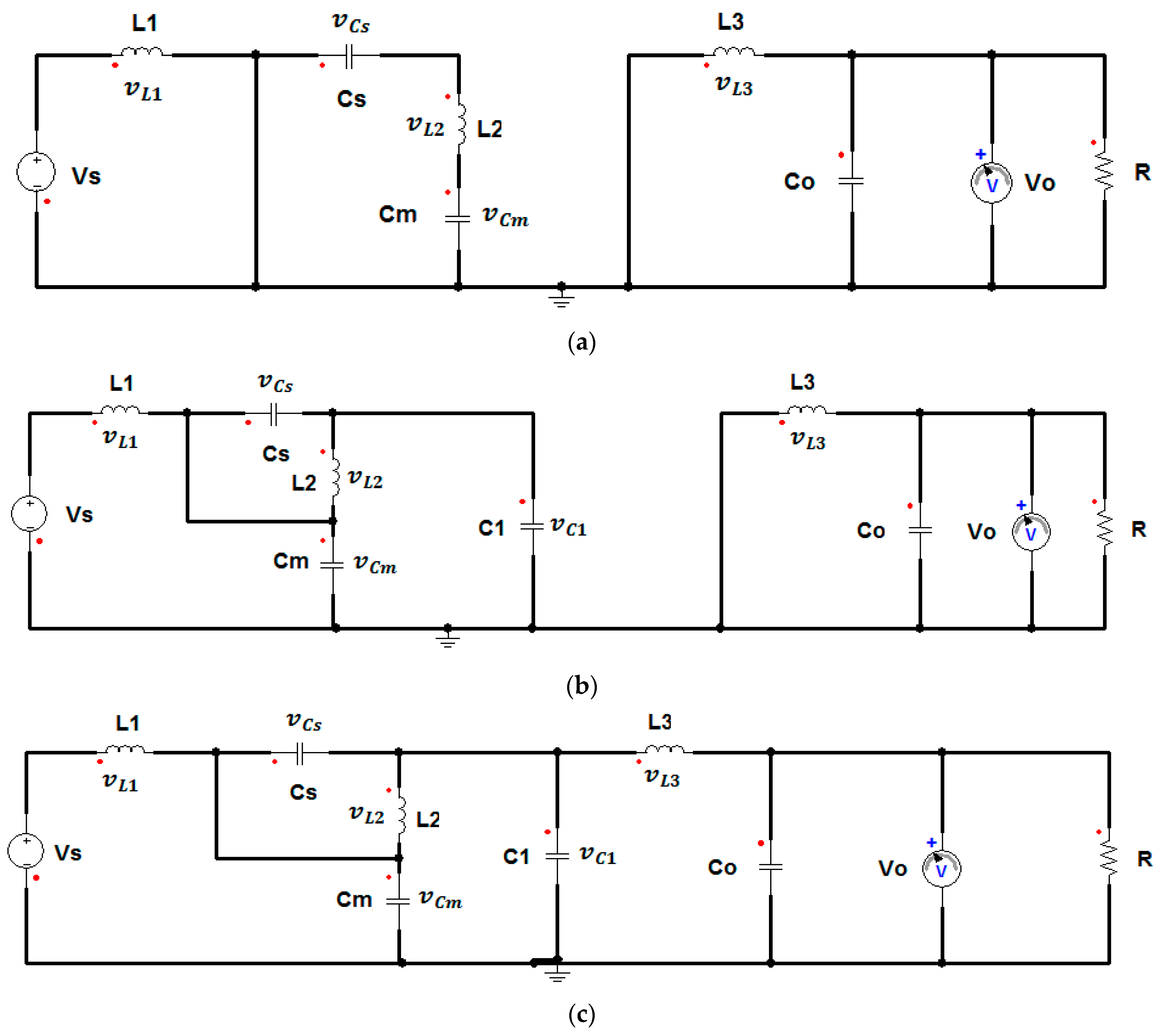
The working principle of the DSSB in the buck regime is better explained using the following circuit diagrams for the region of 0 < D < 1 / 2 :
Based on Figure 2a–c, the DSSB is operating in four stages:
The first stage is shown in Figure 2a [0, DT], during which MOS1 is on. Using the inductor currents as state variables in the following equations to get an expression for the voltage conversion ratio, one may find:
v L 1 = L 1   d i 1 d t = V s                                                     v L 2 = L 2   d i 2 d t = v C s v C m               v L 3 = L 3   d i 3 d t = V o                                          
The second stage is shown in Figure 2b [DT, T/2], during which MOS1 and MOS2 are off. The resultant equations describing this stage are:
v L 1 = L 1   d i 1 d t = V s v C m                                     v L 2 = L 2   d i 2 d t = v C s = v C 1 v C m v L 3 = L 3   d i 3 d t = V o                                                      
The third stage is shown in Figure 2c [T/2, T/2 + DT], during which MOS1 is off and MOS2 is on. The resultant equations describing this stage are:
v L 1 = L 1   d i 1 d t = V s v C m                                                     v L 2 = L 2   d i 2 d t = v C s = v C 1 v C m                 v L 3 = L 3   d i 3 d t = v C 1 V o                                                      
The fourth stage is shown again in Figure 2b [T/2+DT, T], during which MOS1 is off and MOS2 is off. The resultant equations describing this stage are:
v L 1 = L 1   d i 1 d t = V s v C m                                                     v L 2 = L 2   d i 2 d t = v C s = v C 1 v C m                 v L 3 = L 3   d i 3 d t = V o                                                                      
Applying Kirchhoff’s voltage law during these operating stages for the average values of the inductor voltages under steady-state conditions, one finds the following set of equations:
V L 1 = V s 1 D   V c m                                                                                       V L 2 = 1 D V C 1 D V C s   V C m                                                   V L 3 = V o + D   V C 1                                                                     V C s = V C m V C 1                                                                            
Based on the volt-second area balance, the voltages across the inductors have zero average values; therefore, one may find the following relations for the capacitive voltages:
V C m =   1 1 D   V s                                       V C s = D V C m = D 1 D   V s   V C 1 = V o D                                                      
After rearrangement, one may find for the output voltage conversion, Vo, regarding the supply voltage Vs, in the region of 0 < D < 1 / 2 , the following expression:
V o = D   ( 1 + D ) ( 1 D )   V s
The voltage gain characteristics in the bucking regime of the DSSB reach the maximum value when V o = V s . Thus:
V o V s = D   1 + D 1 D = 1 D = 1 + 2  
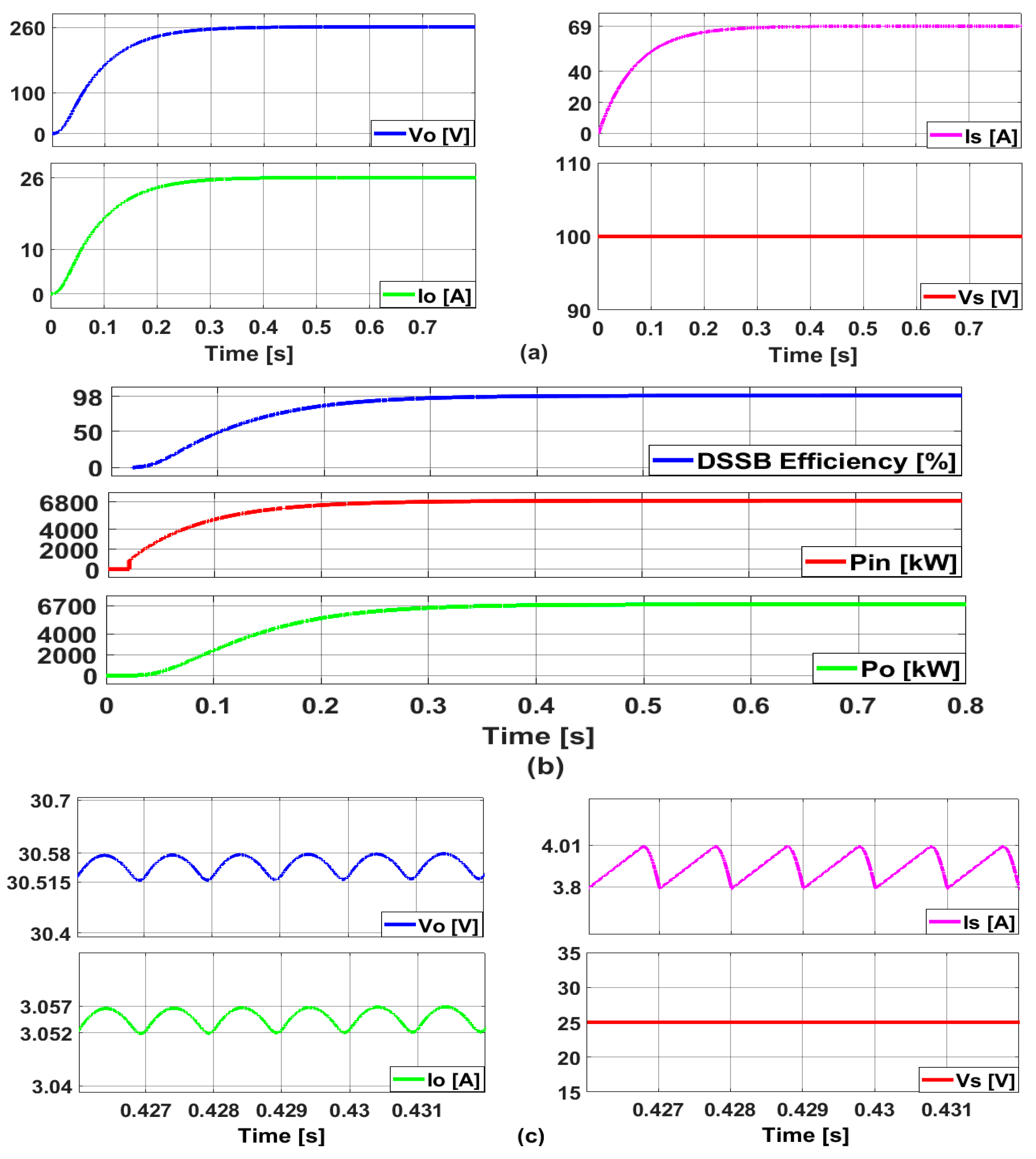
Hence, the output voltage magnitude in the bucking regime is less than that of the supply for 0 < D < 1 + 2 and otherwise, is greater than the supply. Therefore, the DSSB combines the capabilities of the buck and boost converters. The DSSB output and input voltages and currents in the bucking regime are shown in Figure 3a, while the output and input powers with a 98% converter efficiency are shown in Figure 3b. Figure 3c displays the steady-state DSSB voltages and currents waveforms to demonstrate the harmonic content produced in the currents and voltages at low frequency (1 kHz) and supply voltage (25 V).
The voltage and current waveforms for D = 1 / 4 in CCM converter mode are examined and shown in Figure 3a.

2.1.3. Boost-Regime of the DSSB

The second possible operating area of the DSSB is in the region of 2 1 < D < 1 . In this region, the converter is operating exclusively in the mode of boosting regime because its voltage gain can only be greater than unity. The switching times of MOS1 and MOS2 within this region may overlap. Therefore, based on Figure 2a,c and Figure 4a, one may obtain again several stages of operation for the DSSB under the premise of optimal steady-state operating conditions of the DSSB:
The first stage is shown in Figure 4a [0, (2D-1) T]: MOS1 and MOS2 are on during this time interval. To obtain an expression for the voltage conversion ratio, one may use the inductor currents as state variables in the following equations:
v L 1 = L 1   d i 1 d t = V s                                                                                 v L 2 = L 2   d i 2 d t = v C s     v C m                                           v L 3 = L 3   d i 3 d t = v C 1 V o                                                      
The second stage is shown in Figure 2a [0, (1-D) T]: MOS1 is on and MOS2 is off during this time interval. The resultant equations describing this stage are:
v L 1 = L 1   d i 1 d t = V s                                                     v L 2 = L 2   d i 2 d t = v C s v C m               v L 3 = L 3   d i 3 d t = V o                                          
The third stage is shown in Figure 2c [0, (1-D) T]: MOS1 is off and MOS2 is on during this time interval. The resultant equations describing this stage are:
v L 1 = L 1   d i 1 d t = V s v C m                                                     v L 2 = L 2   d i 2 d t = v C s = v C 1 v C m                 v L 3 = L 3   d i 3 d t = v C 1 V o                                                      
Using the same principle of volt-second area, the average voltages across the inductors have zero values, which means:
V L 1 = V s 1 D     V c m                                         V L 2 = D V C s + 1 D V C 1 V C m V L 3 = D   V C 1 V o                                                            
Finally, the voltage conversion ratio can be obtained as follows:
V C m =   1 1 D   V s                                       V C s = D V C m = D 1 D   V s   V C 1 = V o D                                                            
Thus:
V o = D   ( 1 + D ) ( 1 D )   V s
The Matlab/Simulink simulation waveforms for 1 + 2 < D < 1 are shown in Figure 5. The converter efficiency is again 98%, and the switching frequency is f = 10   k H z .
According to Equation (14), the DSSB is operated in the range of 0   D   1 + 2 in the bucking regime to step down the load voltage, Vo, in proportion to the supply voltage, Vs. The DSSB is used to step up the load voltage, Vo, in proportion to the supply voltage, Vs, while the converter is operating in the region of 1 + 2 D   1 .
As a result of the analysis described above, it can be concluded that the output voltage increases when boosting and only slightly decreases when operating in bucking mode. This is because most of the capacitors and inductors in the circuit are accumulated at the input side before the second switch MOSF2. In order to solve this issue, a third MOSFET with the appropriate switching strategy might be used instead of the diode Dm1, although doing so would complicate the structure design of the converter.

2.1.4. The Inductor Current Ripple

The following problems were found by analyzing the previous analogous circuits in light of the inductor current ripple:
In the region of 0 < D < 1 / 2 :
                                                                                                          i 1 = D V s f   L                                                                       i 2 = D ( V C s V C m ) f   L = D V s f   L                                         i 3 = D   V o f   L =   D 2   ( 1 + D ) f   L   ( 1 D )   V s                                        
In the region of 1 / 2 < D < 1 :
i 1 = D V s f   L                                                                                                             i 2 = D ( V C s V C m ) f   L = D V s f   L                                         i 3 = D   V o f   L =   D 2   ( 1 + D ) f   L   ( 1 D )   V s                                        
where f is the switching frequency of the DSSB and L is the common inductance value for all inductors.
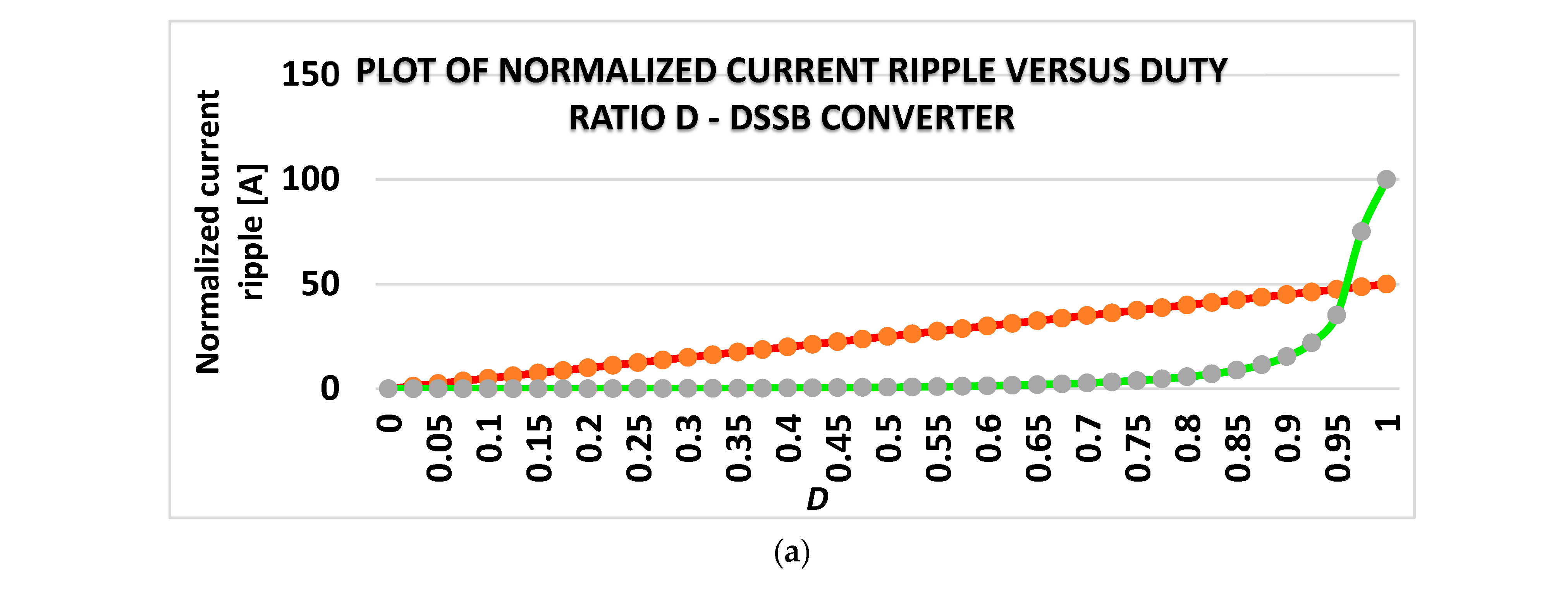
Figure 6a shows an illustration of the DSSB’s normalized inductor current ripple curves for various switching ratio D values. The normalized source current ripple ( i s = i 1 ) of the DSSB is represented by the brown line, and the output current ripple ( i o = i 3 ) is represented by the green line.

2.2. Normalized Voltage Stress of the DSSB Main Switches, MOS1 and MOS2

As a ratio between the reverse voltage of MOS1 and the DSSB supply voltage, Vs, the normalized voltage stress of the DSSB converter switch, MOS1 is described as follows:
V M O S 1 V s = V c m / V s = V C m / V s =   1 1 D    
However, when MOS2 is in the off-state, it has the following normalized voltage stress:
V M O S 2 V s = V c 1 / V s = V C 1 / V s =     ( 1 + D ) ( 1 D )  
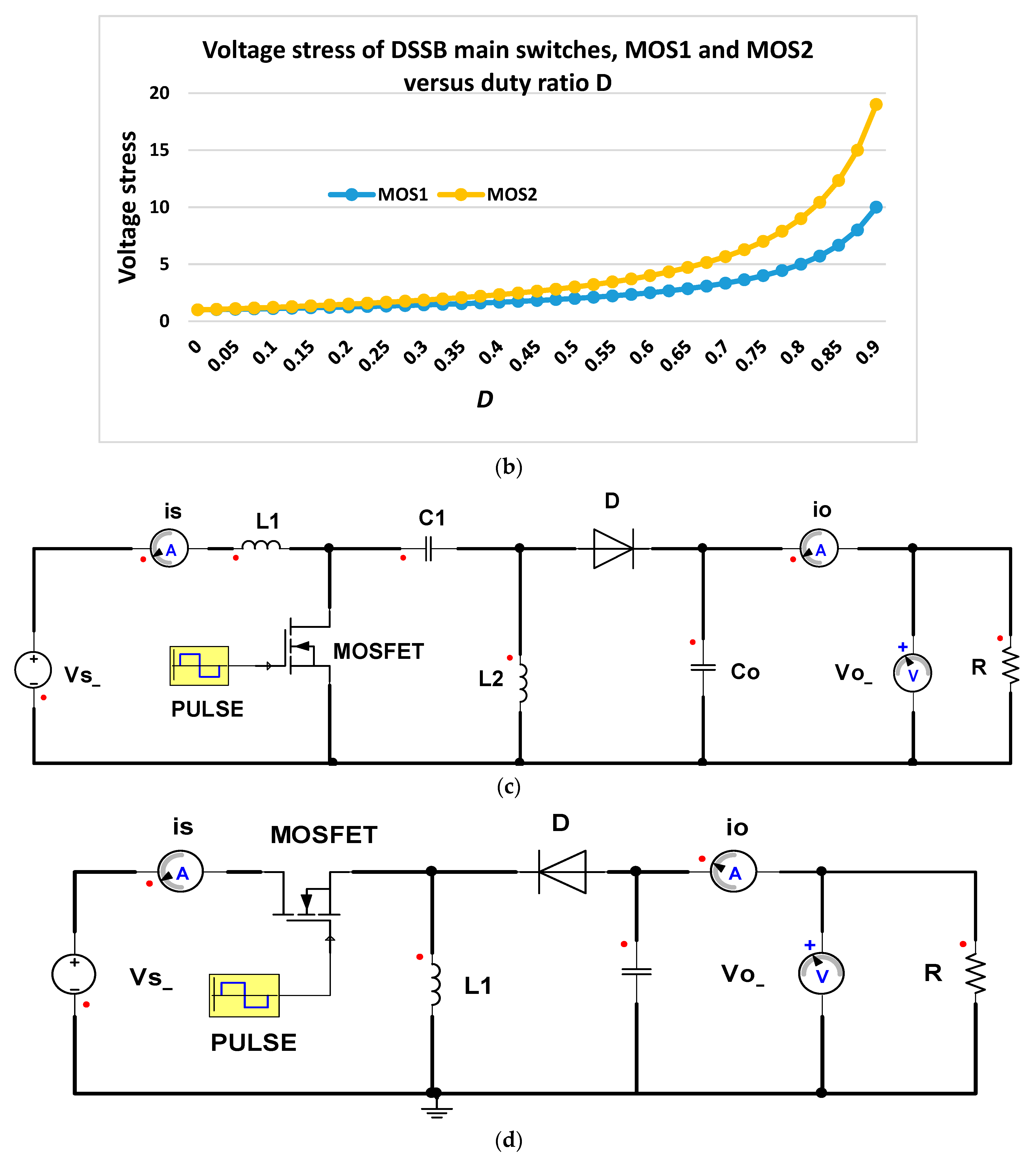
Figure 6b illustrates the normalized voltage stress of the DSSB’s main switches as a function of the increasing switching ratio D using Formulas (17) and (18). When choosing the technical parameters of these switches, it should be remembered that the voltage stress of MOS1 is lower than that of MOS2 based on these figures.
It is wise to compare the voltage stress of the DSSB’s input switch, MOS1, with that of other switched-mode step-down/step-up DC-DC converters to confirm that it is the best option for the industrial applications indicated above. The following expressions can be generated for comparison with the standard SEPIC, depicted in Figure 6c.
When the SEPIC converter main switch, MOSFET, is open, the diode is on. Applying Kirchhoff’s voltage law around the closed loop of Vs, L1, C1, and Vo gives:
V s + v L 1 + v C 1 V o = 0
Because the value of C1 is intentionally very large to keep a voltage across it at the mean of Vs, we get:
v L 1 = V o
Additionally, for the closed loop Vs, L1, with the main switch MOSFET, we get:
V s + v L 1 + v M O S F E T = 0     v M O S F E T = V s + V o
Substituting from [1] for V o = D 1 D into Equation (21), one may get the voltage stress ratio of MOSFET:
v M O S F E T V s = 1 1 D
Similar presumptions to those established for the operation of the DSSB converter are assumed about the voltage stress on the primary switch of the buck-boost converter. The inductor voltage turns on the diode when the main switch is open, allowing current to flow into the load resistor and capacitor. The inductor voltage is at a value of:
v L 1 = V o = D 1 D   V s
Applying Kirchhoff’s voltage law around the closed loop of Vs and L1 yields:
v M S O F E T = V s v L 1 = 1 1 D   V s     v M O S F E T V s = 1 1 D  
According to Formulas (17), (22), and (23), the voltage stress ratio of the conventional SEPIC and buck-boost converters’ main switches is the same as for the DSSB main switch MOS1.
Similar expressions can be obtained for calculating the diode voltage stresses of the DSSB converter and comparing them with conventional SEPIC and boost/buck converters.

3. Comparison of the DSSB Performance with That of Other DC-DC Converters

The most popular non-isolated DC-DC converters are contrasted with the suggested converter in this study. The voltage gain ratio, voltage switch stress, voltage ripple, efficiency, cost, harmonic content, and ease of implementation are crucial elements that were considered throughout the comparison.

3.1. In Comparison to SEPIC and BB Converters

In this section, PWM modulation techniques are used to compare inverting buck-boost (BB), conventional SEPIC, and DSSB converters, in terms of structure complexity, mean value, rectified mean value, total root-mean-square value (RMS) at the fundamental frequency, RMS value of the AC components only (RMSAC), crest factor, ripple factor, harmonic factor, harmonic content distortion, power efficiency, and power factor. The comparison is performed based on the simulation parameters mentioned in Table 1.
The simulation technique used in this paper can be used to calculate distortion and the RMS magnitude at a specified fundamental frequency using real-time analysis and fast Fourier transform (FFT). The root-mean-square value of the fundamental and other components may be calculated either with a Discrete Fourier Transform or with a Least Squares Parameter Estimate. In either case, after determining RMS1 and RMSAC, the root-mean-square value of any component other than the fundamental component is:
R M S k = ( R M S 1 ) 2 + ( R M S A C ) 2   ,   k = 1 ,   2 ,  
where R M S A C is the RMS value of all higher-order components added together, and RMS1 is the RMS value of the fundamental component obtained from the Fourier series analysis.
The total harmonic distortion (THD) is a measure of the harmonic content for any simulation quantity. However, it is necessary to define a period that is used for the computation of the total harmonic distortion. Thus:
T H D = R M S A C 2 R M S 1 2 R M S 1 × 100 %
THD indicates the harmonic content in the tested quantity without any indication of the contributing effect of each harmonic quantity. When a filter circuit is used to withdraw higher harmonics, it is important to know the frequency and amplitude of the remaining higher harmonics to reduce unwanted harmonics without specifying the values of the second-order load filter [3]. This is the result of the harmonic factor (HF), which is a measure of the influence of higher-order components on the harmonic content and is given in the following:
H F = k = 2 ( R M S k ) 2 R M S 1 × 100 %
The crest factor is a function that returns the crest factor (peak/RMS) for the selected simulated quantity, and it is used to measure the peaks in the waveform of the tested quantity. Thus:
K F = k = 2 k 2 ( R M S k ) 2 k = 2 ( R M S k ) 2 × 100 %
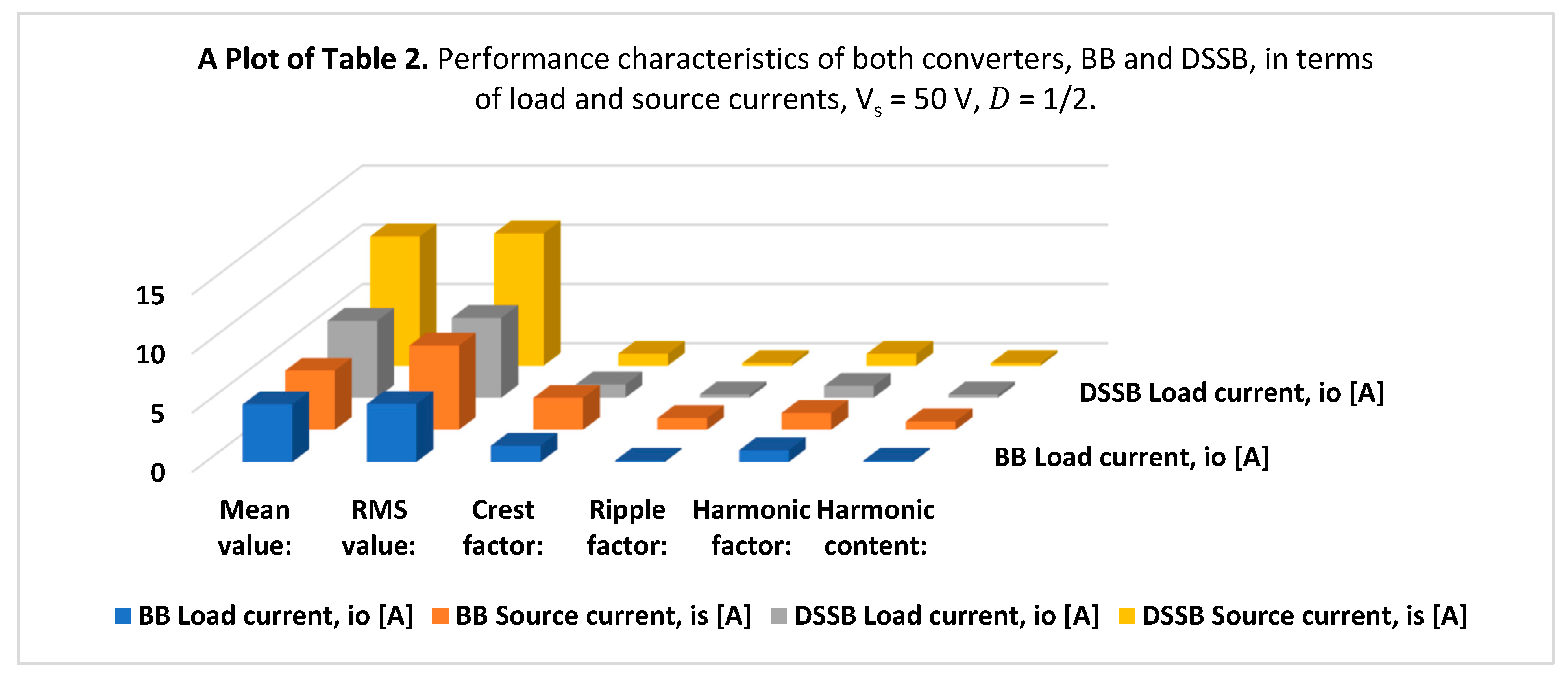
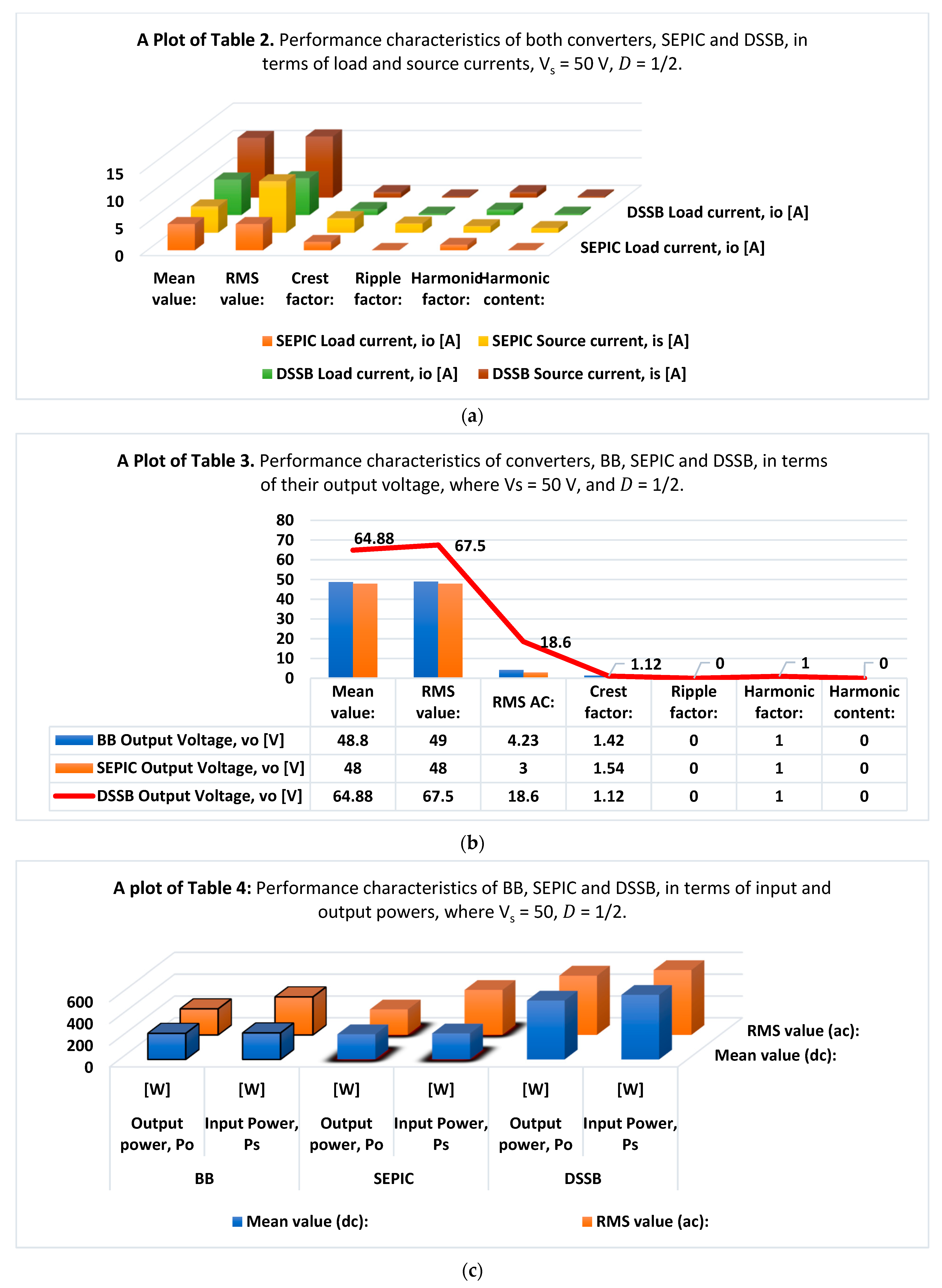
In this study, the effectiveness of the PWM modulation technique for the BB, SEPIC, and DSSB converters is evaluated in terms of the performance characteristics mentioned above as well as those shown in reference Table 2 and Table 3. In Figure 7a,b, the graphical illustration plots of Table 2 and Table 3 provide comparisons of the converter’s dynamic performance.
DC-DC power electronics are frequently used to create pure DC power from pure AC supply systems via rectifier circuits or from DC supply systems that operate periodically. As a result, in addition to the DCs’ average components, the power generated at their outputs also contains various AC and RMS components. Because of this, the converter efficiency—which measures the ratio of DC active power created at the output to supply power—is frequently represented as a percentage of the total DC input power generated. The power factor (PF) of the converter is the proportion of the total input power (RMS and DC average power) to the total output power (RMS and DC average power).
The actual RMS and average values of the input and output powers Ps and Po of the BB, SEPIC, and DSSB converters are calculated and shown in Table 4 and Figure 7c. The average DC power is defined as the amount of power consumed by a DC load, such as a mobile phone battery or DC machinery. The RMS power, also referred to as AC power, is the actual power used by loads such as resistive loads, heaters, lamps, etc. Although having equal and identical DC and RMS power is the primary objective, they are never the same in power electronic systems. In terms of efficiency, harmonic content produced in the converter currents, and voltage gain, the suggested converter DSSB outperforms the BB and conventional SEPIC converters overall.
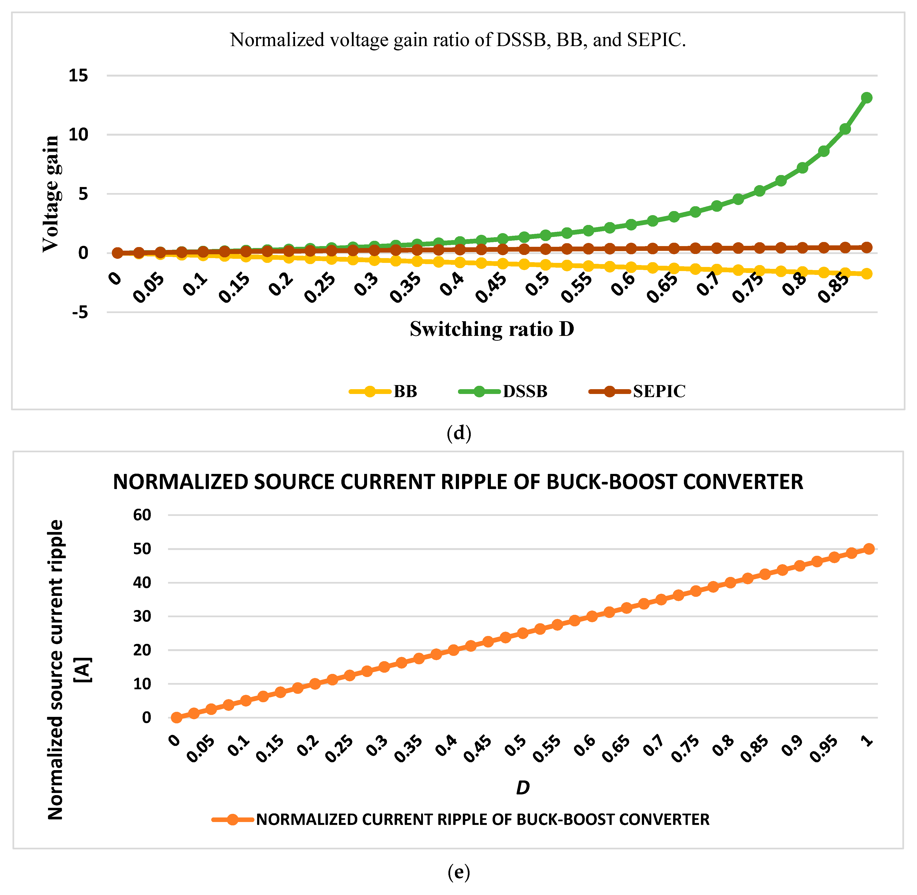
The normalized voltage gain ratio ( V o / V s ), which is illustrated in Figure 7d, is defined as the ratio of the generated output voltage to the converter input voltage. To further contrast the three converters, the switching ratio, D, which is changed from zero to unity, is employed. The normalized voltage gains of the BB and SEPIC converters are used in accordance with [18,19,20], whereas the normalized voltage gain of the DSSB is mentioned in Equation (8).
V o V s = D   1 D = 1 B u c k b o o s t   c o n v e r t e r   ( B B )  
V o V s = D   1 D = 1 S E P I C   c o n v e r t e r  
The suggested converter DSSB has a substantially larger voltage gain ratio than the other two converters, BB and SEPIC. The BB converter’s implementation and use are limited to specific applications because the output voltage is the opposite of the input voltage. As shown in Table 4 and Figure 7d, the power capacity and current/voltage ratings of the DSSB are much larger than those of the BB and SEPIC converters, and it can be used particularly with PV module arrays with higher power [21,22,23,24,25].
Additionally, it would make sense to compare the normalized current ripple for the DSSB source current to that for the BB and SEPIC converters found in [1]. Equations (15) and (16), visually depicted in Figure 7e, clearly match the normalized current ripple produced by the DSSB with that of the BB and SEPIC.

3.2. In Comparison to Other SEPIC Converter Topologies

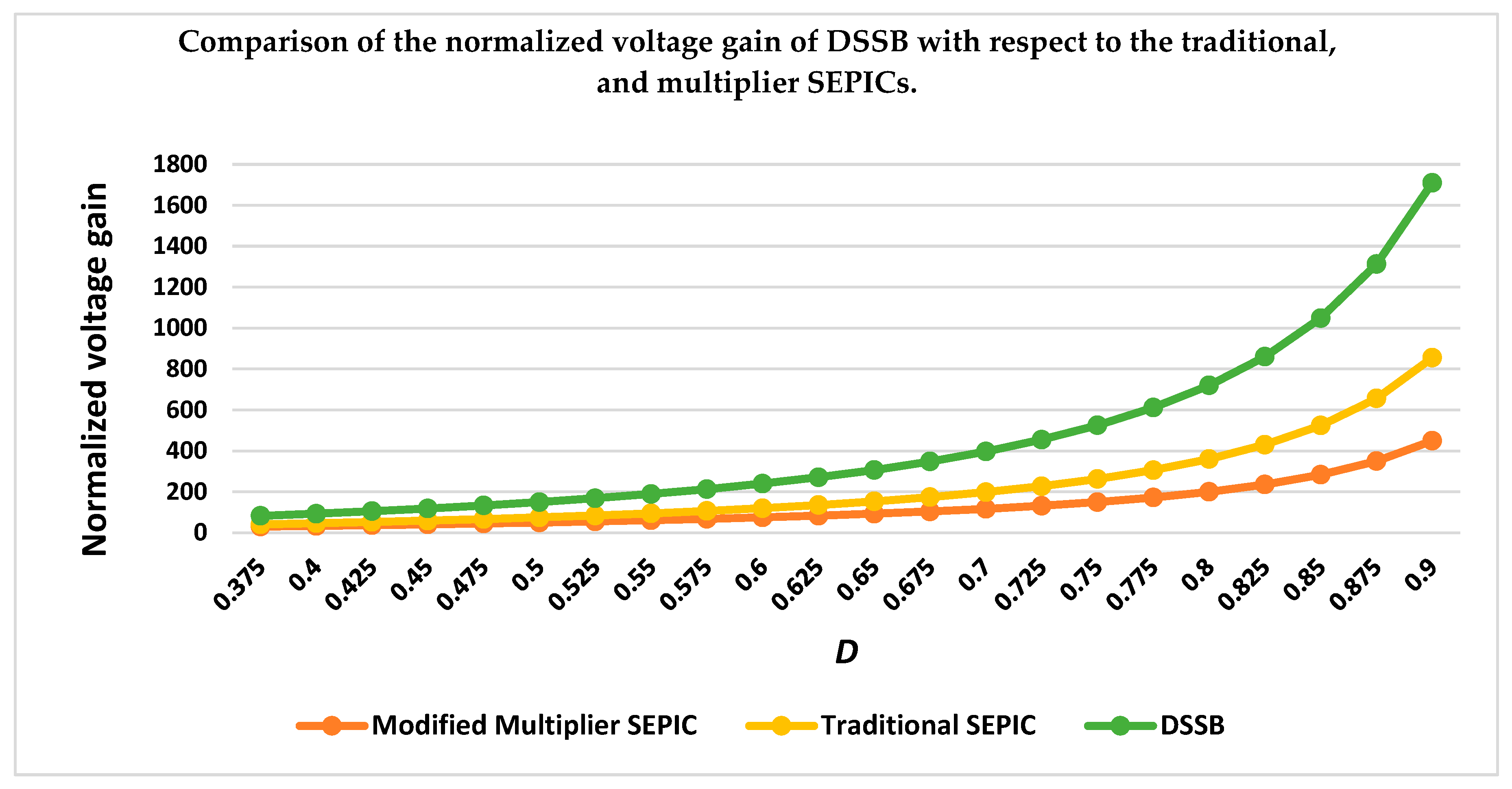
The key observations shown in Table 5 are used to highlight the preference for and technical advantages of the DSSB in light of the aforementioned analysis when compared to alternative SEPIC converter topologies, such as standard and modified multiplier SEPICs. Based on the converter principle of operation requirements, the duty ratio is an adjustable parameter that indicates that the degree of inductor current ripple reduction should be also adjustable.
Figure 8 shows that, when compared to the other SEPIC topologies listed in Table 5, the normalized voltage gain with the updated DSSB conversion processor is much better. The conversion ratio D = 0 produced the lowest value of this ripple, whereas D = 1 theoretically produced the highest. Additionally, as the duty cycle, D, gets closer to unity, the maximum ripple percentage of the output voltage content increases dramatically.

4. Control Method of DSSB Converter

This section outlines the proposed DSSB converter control strategy and illustrates a power factor correction strategy based on the regulation of the input-output current and the voltage of the DSSB. As a result, the converter efficiency is improved, and the overall harmonic content of the input-output voltages and current is decreased.

4.1. AC Small-Signal Analysis Technique

The AC small-signal technique is used to approximate the behavior of the converter, such as a linear time-invariant system around a certain switching cycle of the switches as the operating point of interest. This AC small-signal principle enables the DSSB duty cycle representations through open-loop and closed-loop transfer functions [25,26,27,28].
Once the frequency response of the DSSB simulation model is determined in Simplorer 7, its open-loop and closed-loop transfer functions are estimated. A suitable compensator is then designed and evaluated based on the linear model. By repeating the small-signal technique for different operating points (for example, different switching (duty) cycle ratios or desired output voltage levels), the gain of the controller was selected for the DSSB operation in the desired operating range. The small-signal model may be created and verified in algorithm form as follows [29,30]:
  • Several perturbation input voltages and currents are selected to perform the DSSB small-signal analysis.
  • A compensator for the resulting linear model is designed and tuned using techniques such as automatic PI tuning or interactive loop shaping, with the original locus and Bode plots.
  • A programmed gain compensator is created to operate the power electronic system under all possible operating conditions.
  • The design of the controller is verified and tried by simulating it against the non-linear power electronic system model.
  • Instead, a simulation built using the non-linear DSSB model is used to verify and validate the implementation of the controller design.
  • A MATLAB and Simplorer 7 models are automatically generated for rapid prototyping and production control system implementation.
Based on the algorithmic procedure explained above, the converter output quantities (source voltages, and currents) are partitioned into the averaged DC and low-frequency AC components as follows:
First, the average values of their present and previous instantaneous values for every switching cycle, T = 1 f , are calculated as follows:
X n = 1 T n T ( n + 1 ) T x d t               X n 1 = 1 T ( n 1 ) T ( n ) T x d t
Applying the circuit averaging method and after neglecting the nonlinear terms, the small-signal voltages of inductors L1, L2, and L3 can be written as follows:
v ~ L 1 t = V s + v ~ s t + D 1 + V C M + v ~ C M t + d ~ ( t ) V C M
v ~ L 1 t = V s + v ~ s t + D 1 V C M + v ~ C M t + d ~ ( t ) V C M                          
v ~ L 2 t = D V s + v ~ s t D V C s + v ~ C s t + 1 D V C 1 + v ~ C 1 t 1 + D V C M + v ~ C M t + d ~ ( t ) [ V C M V s V C s V C 1 ]
v ~ L 3 t = V o + v ~ o t + D V C + v ~ C t + d ~ ( t ) V C
where the term v ~ indicates the small-signal component of the respective voltage. Thus, the open-loop voltage gain (transfer function) is given as:
G v s = V o / V r e f = k p v × G a s = 12.5 × 8 × 10 6   1 + 0.02 S 3  
The open-loop current gain (transfer function) is given as:
  G i s = I o / I r e f = k p i × G b s = 25 × 1 × 10 4 S   1 + 0.01 S 2  
Second, the average present and prior values of the relevant load currents and voltages are multiplied to determine the values of the present and the preceding load powers.
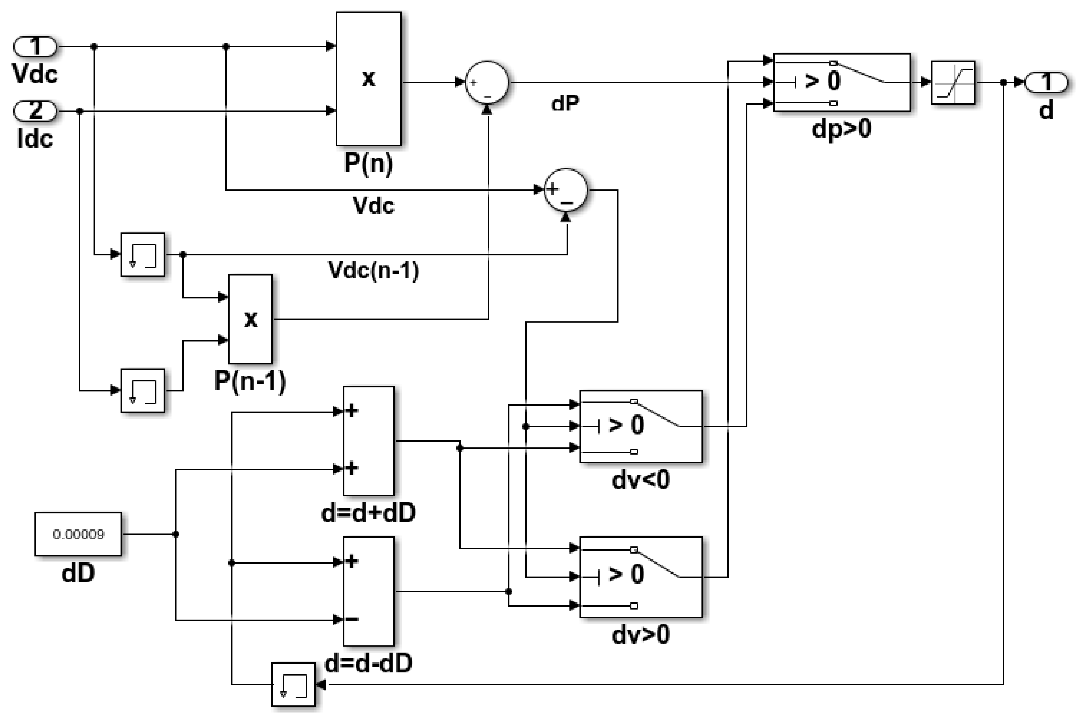
Thus, the DC load voltage, current, and mutual product at each moment, as well as the duty cycle D, may therefore be perturbed at a frequency that is lower than the converter’s switching frequency. All other conversion variables will therefore oscillate at this frequency around their respective DC values. As a result, the switching method depicted in Figure 9 is used to determine the averaged load voltages, currents, and duty cycle.
The DSSB control algorithm constantly monitors how rapidly the power changes in proportion to variations in load voltage and current. The DC-DC DSSB converter is optimized to provide the least amount of load current and voltage ripple and to achieve the highest possible power transfer efficiency. The output of this AC small-signal controller is then delivered to the converter PWM signal generator, to produce a duty ratio that is D ≤ 1.

4.2. Current-Mode Technique Based on AC Small-Signal Analysis

The term “AC small-signal analysis with voltage-current mode technique” or simply “current-mode technique based on AC small-signal” refers to the second method of controlling the power and voltage in the DSSB system. The control structure of such a technique requires two additional loops in addition to the AC small-signal technique, one internal current source loop, and one external voltage source loop. In this approach, a small-signal algorithm is first provided as explained earlier, and then the DSSB load voltage is controlled by a dedicated control scheme using a PI controller. The current-mode controller operates on the difference between the load voltage setpoint and its measured actual value. Then, the load current is controlled by comparing its measured value with its desired value generated from the load voltage control scheme [31,32].
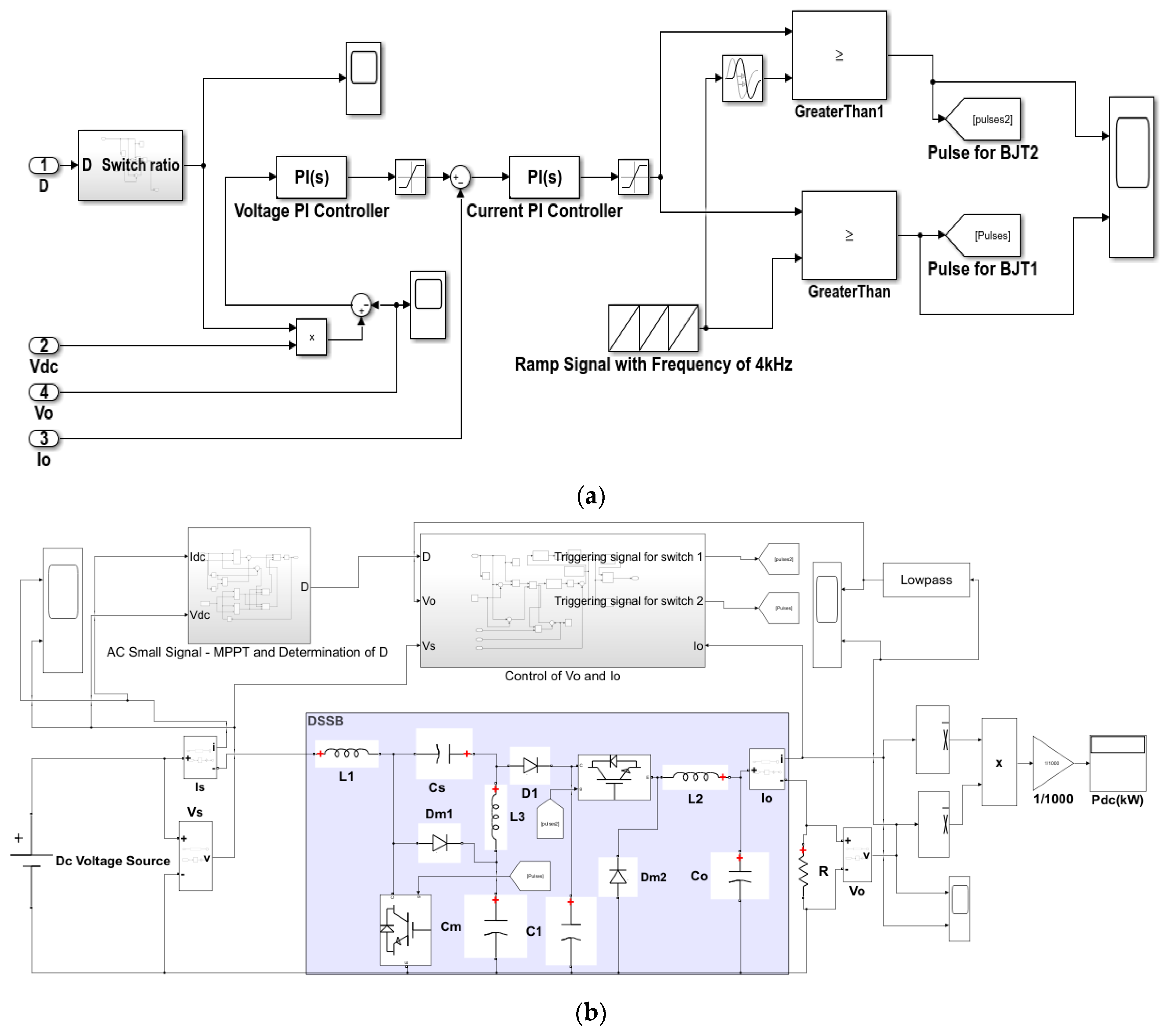
Thus, the DSSB input inductor currents and voltage are sensed and controlled to produce the required output power with a value corresponding to the acceptable and possible normalized input power based on the small-signal technique. Then, to achieve the desired load current and load output voltage with very low ripple, the gate signals for the DSSB switches are generated using a current-mode control technique using proper PWM with two ramp signals phase-shifted by 180° in sequence.
The control block diagram for the DSSB with two PI controllers to regulate the load current and voltage is shown in Figure 10a. The DSSB circuit is depicted in Figure 10b together with the current-mode control and the AC small-signal analysis control blocks.

5. Simulation Results

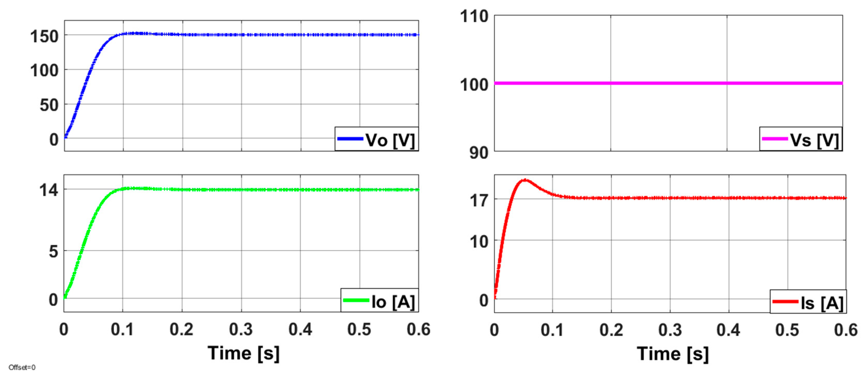
To validate the analytical study and theoretical simulation, a thorough investigation into the DSSB converter used in the CCM using the parameters listed in Table 6 was conducted. The waveforms of the source/load current and voltage shown in Figure 11 are entirely identical to the simulated waveforms shown in Figure 5b. The converter operates in direct current mode (CCM) because its current does not reach zero during the entire conversion period, while the ripple of each current corresponds to the device specifications.
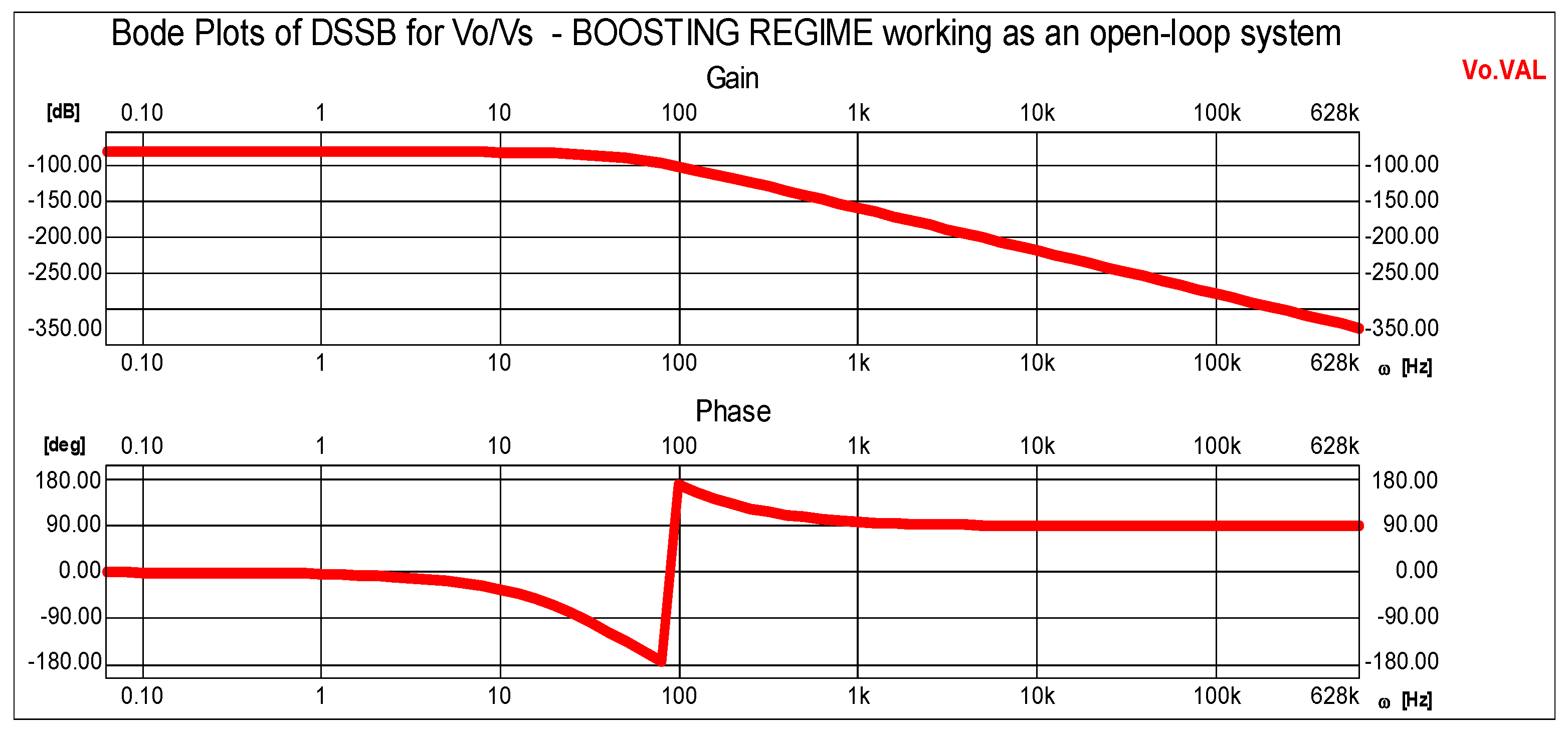
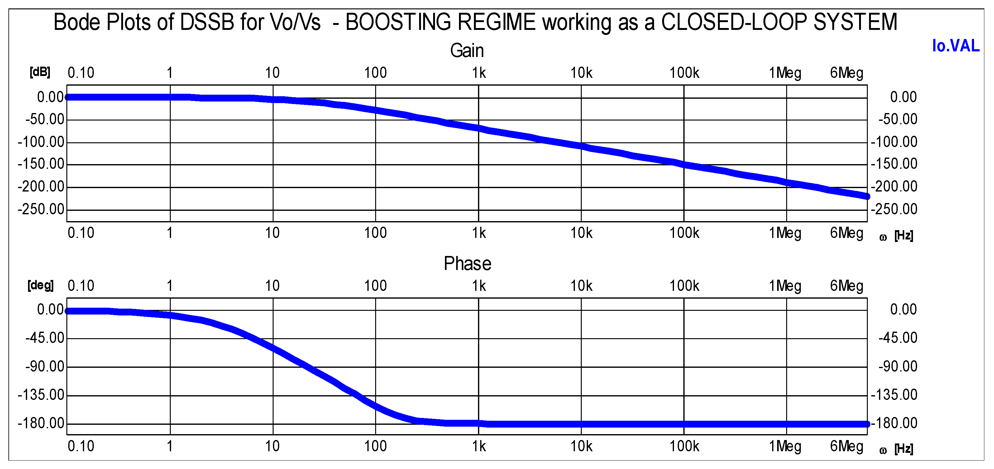
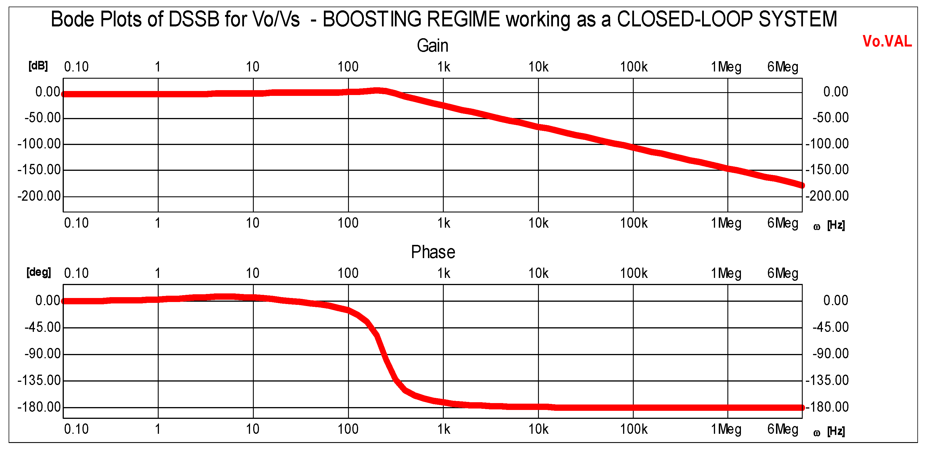
The important aspect to be investigated is the frequency response of the system that is used to determine the stability of the system. Here, one can use two quantities, gain margin and phase margin, which indicate the amplitude of the system before it becomes stable or unstable. The bode plots of the open-loop current gain transfer function I o / I s and voltage gain V o / V s for the DSSB is shown in Figure 12, Figure 13, Figure 14 and Figure 15.
The phase margin for a closed loop system is the additional amount of phase delay required for the phase of the open loop system to reach −180° at a frequency where the magnitude of the open loop system is 0 dB.
The Bode diagrams of the closed-loop system in Figure 11, Figure 12, Figure 13 and Figure 14 and MATLAB/Simulink together with Simplorer 7 demonstrate that the DSSB system is stable since the zero crossing of 0 dB happened at a phase angle (phase margin) that is less than 180°, or 55°. Additionally, as seen in Figure 14, the gain margin at the −180° crossing is greater than zero and is around 82 dB.
Additionally, the closed-loop system output voltage is constructed so that its bandwidth, as indicated by the closed-loop transfer function, is 355 Hz. The phase crossover frequency for the voltage gain transfer function is around 23 kHz, and for the current gain, it is approximately 700 Hz, as can be seen in Figure 13 and Figure 14. For frequencies below 1 MHz, the gain roll-off rate (slope) is −40 db/decade, which is equal to a rate of −24 db/octave. From the current loop plot, the converter may behave as an underdamped system with two real negative poles and one pole at the origin, which can be observed from the current gain transfer function [33,34].
Table 6. DSSB design specifications [35].
ParameterSymbolReal valueType
Input VoltageVs50 VDC power source
Input InductorL1(100–400) mHCore NEE-65/33 by Thornton, NL1 = 180 turns − 4 × AWG 27
Input inductor current ripple∆iL10.12 A-
Output inductor current ripple∆iL30.08 A-
Shunt InductorL320 mHCore NEE-65/33 by Thornton, NL2 = 180 turns − 4 × AWG 27
Output InductorL220 mHcore NEE-65/33 by Thornton, NL3 = 45 turns − 5 × AWG 24
Smoothing capacitorCs940 uFElectrolytic capacitor by Hitano
Shunt capacitorCm940 uFElectrolytic capacitor by Nichicon
Shunt capacitorC1940 uFElectrolytic capacitor by Nichicon
Output capacitorCo3.33 mFElectrolytic capacitor by Hitano
Switching ratioD0.4-
Output voltage:Vo25 V-
Load resistance:R10 ΩCeramic resistor by LW
Switching frequency:f4 kHzSignal generator
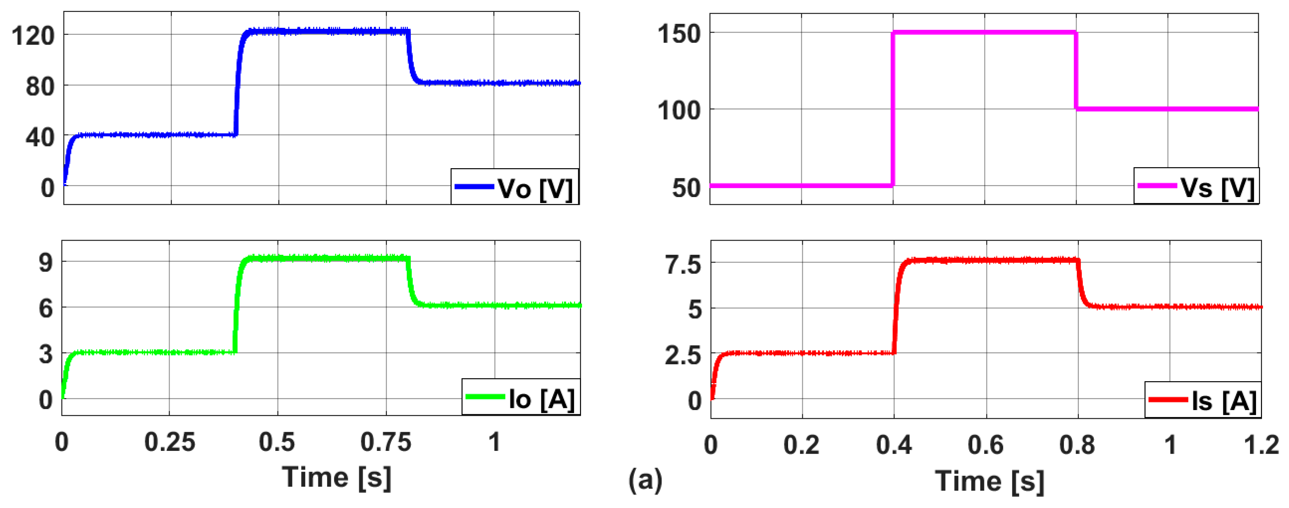
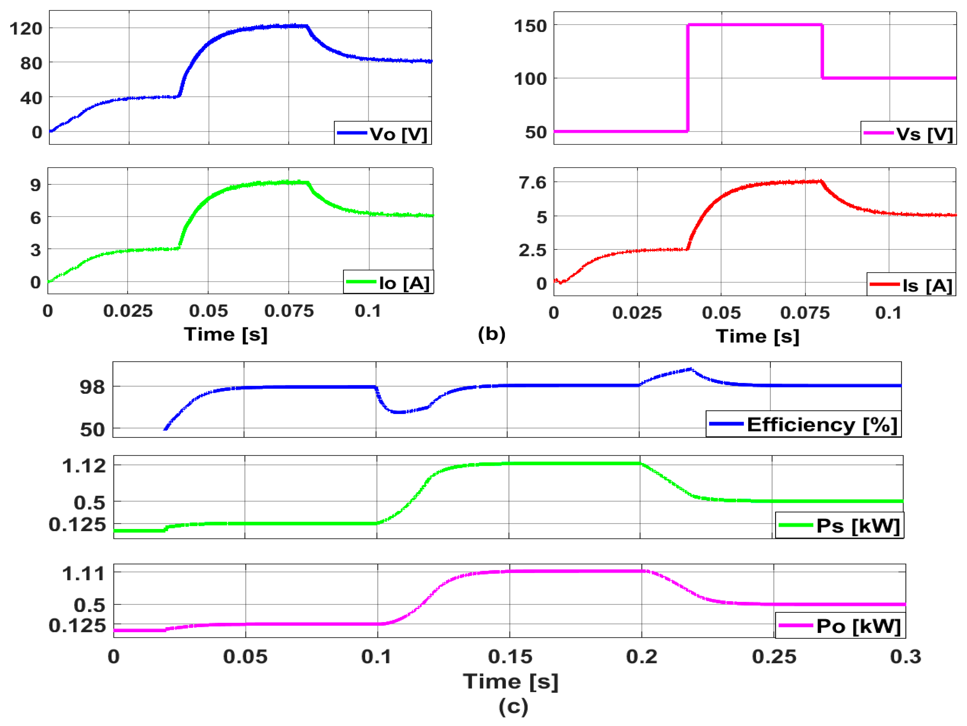
Figure 16 depicts the dynamic response of the DSSB input/output voltage and current waveforms for a variable step response of the input source voltage using the parameters listed in Table 6. Figure 16b displays a compressed timeline of the output voltage and the current transient response to demonstrate the time specifications and requirements of the response, and Figure 16c is used to demonstrate the effectiveness of the current-mode controller based on small-signal analysis.
The simulation of Figure 16 shows that the DSSB responds very well in terms of output voltage and current simulated waveform because the output voltage and current waveform precisely match the step change in the input voltage and current. Slow overshoot, decreased settling time, and rise time are all characteristics of DSSB-responsive behavior, which should lead to better frequency response. This is evident from the narrower timeframe for a temporary (transitory) response, which is also displayed in Figure 16 for the output voltage and current.

6. Conclusions

This study introduces a double-switch SEPIC-buck converter (DSSB) with a new topology. This new topology can be applied to step-up applications as well as step-down applications of PV solar systems, wind turbine systems, and other similar industrial applications. The converter design employs two active switches, which causes minimal sag and ripple in the input and output inductor currents and voltages. The proposed DSSB converter produces minimal harmonic content with consistent input/output power and efficiency, in contrast to traditional DC-DC converters.
The suggested converter dynamic performance is optimized using a current-mode, control-based, small-signal analysis with two dual-lead PI controllers. A control circuit that incorporates both an open-loop and closed-loop DSSB frequency response is also suggested and shown to work properly. The small-signal technique has been implemented in the DSSB simulation model to represent its dynamic behavior through the frequency response and transfer functions.
There are several advantages to be gained from representing a small-signal analysis with a current-mode control technique through a frequency response:
  • Using the current-mode control technique, it is possible to regulate the inductor current’s peak-to-peak ripple as well as its mean value, which is an advantage of the current-mode control technique based on small-signal analysis.
  • Another advantage is that the higher-order system control used to produce the frequency response of such a converter is reduced to the second-order frequency response.
The proposed current-mode control technique based small-signal analysis is validated by subjecting the proposed converter to unique operating conditions, such as providing it with a variable step input and analyzing its dynamic response. The outcomes demonstrate the DSSB converter’s robustness to changes in its parameters, as well as its improved dynamic performance and increased control precision, which are further advantages of this converter.
Additionally, a comparison study between the DSSB converter and the different topologies of the SEPIC converter, including some other DC-DC converters like buck, boost, buck-boost, and others, has also been given. The complexity, voltage stress on the converter active switches, mean and rectified mean values, RMS values, crest and ripple factors, harmonic factors, and harmonic content distortion are all compared. Because of its superior input/output power response, lower ripple factor, lower harmonic content, highest output efficiency, close to unity power factor, reduced current ripple, and overall better dynamic performance, the study concludes that the proposed converter, designated DSSB, might be a competitive option for industrial applications.

Author Contributions

Conceptualization, W.E.; methodology, W.E.; software, W.E.; validation, W.E., H.I., H.K., O.F. and H.A.; formal analysis, W.E. and O.F.; investigation, W.E. and H.K.; resources, W.E.; data curation, W.E.; writing—original draft preparation, W.E.; writing—review and editing, W.E. and H.A.; visualization, W.E. and H.I.; supervision, W.E.; project administration, W.E.; funding acquisition, W.E., H.I., H.K., O.F. and H.A. All authors have read and agreed to the published version of the manuscript.

Funding

This research received no external funding.

Data Availability Statement

All data generated or analyzed during this study are included in this published article.

Acknowledgments

All authors would like to thank Ayman Amer for financial support.

Conflicts of Interest

The authors declare no conflict of interest.

References

  1. Hart, D.W. Power Electronics, International Edition; McGraw Hill: New York, NY, USA, 2011. [Google Scholar]
  2. Rahbar, K.; Xu, J.; Zhang, R. Real-time energy storage management for renewable integration in microgrid: An off-line optimization approach. IEEE Trans. Smart Grid 2014, 6, 124–134. [Google Scholar] [CrossRef]
  3. Rahbar, K.; Chai, C.C.; Zhang, R. Energy cooperation optimization in microgrids with renewable energy integration. IEEE Trans. Smart Grid 2016, 9, 1482–1493. [Google Scholar] [CrossRef]
  4. Vadivel, S.; Ragupathy, U.S. Modeling and Design of High-Performance Converters for Optimal Utilization of Interconnected Renewable Energy Resources to Micro Grid with GOLRS Controller. Int. J. Control Autom. Syst. 2021, 19, 63–75. [Google Scholar] [CrossRef]
  5. Li, H.; Liu, C.; Zhang, X.; Guo, Z.; Zheng, T.Q. Stability Analysis for Two-Stage Cascaded DC-DC Converters System Based on Describing Function Method. In Proceedings of the 2018 IEEE Energy Conversion Congress and Exposition (ECCE), Portland, OR, USA, 23–27 September 2018; pp. 4141–4147. [Google Scholar] [CrossRef]
  6. Azer, P.; Emadi, A. Generalized State Space Average Model for Multi-Phase Interleaved Buck, Boost and Buck-Boost DC-DC Converters: Transient, Steady-State and Switching Dynamics. IEEE Access 2020, 8, 77735–77745. [Google Scholar] [CrossRef]
  7. Yalçin, F.; Yazici, İ. Robust Discrete-Time Hybrid Controller for Non-Inverting Buck-Boost DC-DC Converter. Sak. Univ. J. Sci. 2023, 27, 68–82. [Google Scholar] [CrossRef]
  8. Wu, J.; Mo, M.; Li, J.; Zhang, Y.; Zhang, X.; Fan, X. Inverse decoupling internal model control for multilevel buck converter with constant power load. Energy Rep. 2023, 9 (Suppl. 7), 1181–1189. [Google Scholar] [CrossRef]
  9. Hao, Y.; Guo, K.; Liu, L.; Cai, W.; Liu, F. improved cubic boost converter based on voltage closed-loop control. Energy Rep. 2022, 8 (Suppl. 6), 87–95. [Google Scholar] [CrossRef]
  10. Vinay Kumar, C.; Rao, G.M.; Raghu Ram, A.; Prasanna Kumar, Y. Designing of Neuro-Fuzzy Controllers for Brushless DC Motor Drives Operating with Multiswitch Three-Phase Topology. J. Electr. Comput. Eng. 2022, 2022, 7001448. [Google Scholar] [CrossRef]
  11. Al Attar, H.; Hamida, M.A.; Ghanes, M.; Taleb, M. Review on Modeling and Control Strategies of DC–DC LLC Converters for Bidirectional Electric Vehicle Charger Applications. Energies 2023, 16, 3946. [Google Scholar] [CrossRef]
  12. Solis-Rodriguez, J.; Rosas-Caro, J.C.; Alejo-Reyes, A.; Valdez-Resendiz, J.E. Optimal Selection of Capacitors for a Low Energy Storage Quadratic Boost Converter (LES-QBC). Energies 2023, 16, 2510. [Google Scholar] [CrossRef]
  13. Kalimuthu; Ramkumar, M.S.; Amudha, A.; Balachander, K.; Krishnan, M.S. A High Gain Input-Parallel Output-Series Dc/Dc Converter with Dual Coupled-Inductors. Math. Comput. For. Nat. Resour. Sci. 2019, 11, 242–246. [Google Scholar]
  14. Dagal, I.; Akın, B.; Akboy, E. MPPT mechanism based on novel hybrid particle swarm optimization and salp swarm optimization algorithm for battery charging through simulink. Sci. Rep. 2022, 12, 2664. [Google Scholar] [CrossRef] [PubMed]
  15. Seyezhai, R.; Mathur, B.L. A Comparison of Three-Phase Uncoupled and Directly Coupled Interleaved Boost Converter for Fuel Cell Applications. Int. J. Electr. Eng. Inform. 2011, 3, 394–407. [Google Scholar] [CrossRef]
  16. Reatti, A.; Corti, F.; Tesi, A.; Torlai, A.; Kazimierczuk, M.K. Effect of Parasitic Components on Dynamic Performance of Power Stages of DC-DC PWM Buck and Boost Converters in CCM. In Proceedings of the 2019 IEEE International Symposium on Circuits and Systems (ISCAS), Sapporo, Japan, 26–29 May 2019; pp. 1–5. [Google Scholar] [CrossRef]
  17. Zhang, W.; Liu, Y.; Li, Z.; Zhang, X. The dynamic Power Loss analysis in Buck Converter. In Proceedings of the 2009 IEEE 6th International Power Electronics and Motion Control Conference, Wuhan, China, 17–20 May 2009; pp. 362–367. [Google Scholar] [CrossRef]
  18. Trakuldit, S.; Tattiwong, K.; Bunlaksananusorn, C. Design and evaluation of a quadratic Buck Converter. Energy Rep. 2022, 8 (Suppl. 1), 536–543. [Google Scholar] [CrossRef]
  19. Emar, W.; Huneiti, Z.; Hayajneh, S. Analysis, Synthesis and Simulation of Compact Two-channel Boost Converter for Portable Equipments Operating with a Battery or Solar Cell. Procedia Comput. Sci. 2015, 65, 241–248. [Google Scholar] [CrossRef]
  20. Emar, W. Analysis, modeling and simulation of step-up converter using Matlab-Simulink and simplorer. Int. J. Model. Simul. Sci. Comput. 2016, 7, 1650004:1–1650004:13. [Google Scholar] [CrossRef]
  21. de Dieu Nguimfack-Ndongmo, J.; Ngoussandou, B.P.; Goron, D.; Asoh, D.A.; Kidmo, D.K.; Nfah, E.M.; Kenné, G. Nonlinear neuro-adaptive MPPT controller and voltage stabilization of PV Systems under real environmental conditions. Energy Rep. 2022, 8 (Suppl. 9), 1037–1052. [Google Scholar] [CrossRef]
  22. Zaid, M.; Khan, S.; Mahmood, A.; Ali, M.; Sarwar, A.; Khalid, M. A New High Gain Boost Converter with Common Ground for Solar-PV Application and Low Ripple Input Current. Arab. J. Sci. Eng. 2023, 48, 14655–14669. [Google Scholar] [CrossRef]
  23. Raj, T.A.B.; Ramesh, R.; Maglin, J.R.; Vaigundamoorthi, M.; Christopher, I.W.; Gopinath, C.; Yaashuwanth, C. Grid Connected Solar PV System with SEPIC Converter Compared with Parallel Boost Converter Based MPPT. Int. J. Photoenergy 2014, 2014, 385720. [Google Scholar] [CrossRef]
  24. Attar, H.; Kamarposhti, M.A.; Solyman, A.A.A. Impacts of integration of wind farms on voltage stability margin. Int. J. Electr. Comput. Eng. (IJECE) 2022, 12, 4623–4631. [Google Scholar] [CrossRef]
  25. Iqteit, N.A.; Yahya, K.; Makahleh, F.M.; Attar, H.; Amer, A.; Solyman, A.A.A.; Qudaimat, A.; Tamizi, K. Simple Mathematical and Simulink Model of Stepper Motor. Energies 2022, 15, 6159. [Google Scholar] [CrossRef]
  26. Bairabathina, S.; S, B. Design and Validation of a SEPIC-Based Novel Multi-Input DC-DC Converter for Grid-Independent Hybrid Electric Vehicles. Energies 2022, 15, 5663. [Google Scholar] [CrossRef]
  27. Iqbal, D.; Siddique, M.; Chaudhary, A.; Liaqat Bhatti, K.; Abrar, M.; Hussain, M. Novel Concept of Reducing OVR at the Output of SEPIC Converter using Programmable Capacitors. Int. J. Electr. Eng. Inform. 2021, 13, 477–494. [Google Scholar] [CrossRef]
  28. Komathi, C.; Umamaheswari, M.G. Analysis, and design of genetic algorithm-based cascade control strategy for improving the dynamic performance of interleaved DC–DC SEPIC PFC converter. Neural Comput. Appl. 2020, 32, 5033–5047. [Google Scholar] [CrossRef]
  29. Senthilkumar, R.; Justin Sunil Dhas, G. Fractional order controller design for SEPIC converter using metaheuristic algorithm. J. Intell. Fuzzy Syst. 2018, 35, 6269–6276. [Google Scholar] [CrossRef]
  30. Kwon, J.-M.; Choi, W.-Y.; Lee, J.-J.; Kim, E.-H.; Kwon, B.-H. Continuous-conduction-mode SEPIC converter with low reverse-recovery loss for power factor correction. IEE Proc. Electr. Power Appl. 2006, 153, 673–681. [Google Scholar] [CrossRef]
  31. Dalimunthe, A.M.A.; Sara, I.D.; Tarmizi. Adaptive Control for SEPIC Converter. In Proceedings of the 2020 4rd International Conference on Electrical, Telecommunication and Computer Engineering (ELTICOM), Medan, Indonesia, 3–4 September 2020; pp. 92–96. [Google Scholar] [CrossRef]
  32. Hu, J.; Sagneri, A.D.; Rivas, J.M.; Han, Y.; Davis, S.M.; Perreault, D.J. High-Frequency Resonant SEPIC Converter with Wide Input and Output Voltage Ranges. IEEE Trans. Power Electron. 2012, 27, 189–200. [Google Scholar] [CrossRef]
  33. Weitz, N.; Utzelmann, S.; Ditze, S.; März, M. A Resonant Push–Pull DC–DC Converter With an Intrinsic Current Source Behavior for Radio Frequency Power Conversion. IEEE Trans. Power Electron. 2022, 37, 7001–7012. [Google Scholar] [CrossRef]
  34. Yang, Y.; Liu, Y.; Zhao, Y.; Liu, J.; Zhu, B. High frequency and high-power density bipolar DC–DC converter with GaN HEMT. Energy Rep. 2023, 9 (Suppl. 7), 617–624. [Google Scholar] [CrossRef]
  35. Amer, A.; Attar, H.; As’ad, S.; Alsaqoor, S.; Colak, I.; Alahmer, A.; Alali, M.; Borowski, G.; Hmada, M.; Solyman, A. Floating Photovoltaics: Assessing the Potential, Advantages, and Challenges of Harnessing Solar Energy on Water Bodies. J. Ecol. Eng. 2023, 24, 324–339. [Google Scholar] [CrossRef]
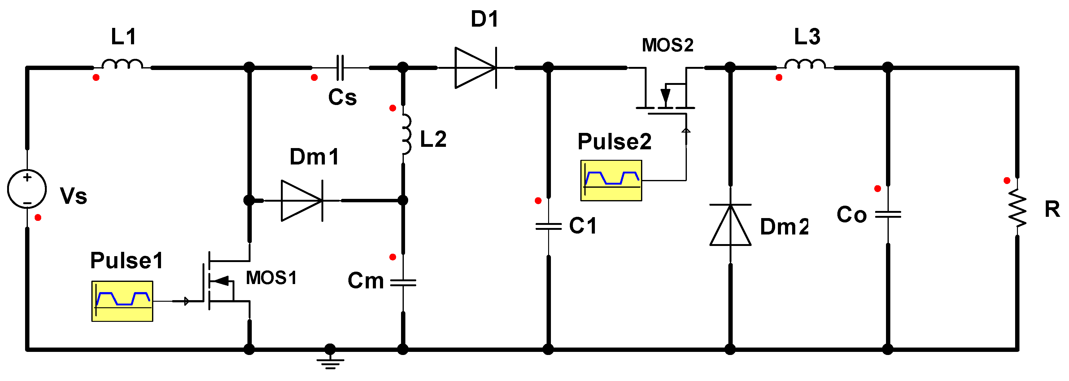
Figure 1. DSSB converter.
Energies 17 00238 g001
Figure 2. (a) On-state of MOS1 and off-state of MOS2 in the operating region of 0 < D < 1 / 2 , (b) Off-state of MOS1 and MOS2 in the operating region of 0 < D < 1 / 2 , (c). Off-state of MOS1 and on-state of MOS2 for the operating region of 0 < D < 1 / 2 .
Energies 17 00238 g002
Figure 3. MATLAB/Simulink simulation of the DSSB in the bucking region of 0 < D < 2 1 : (a) Output and input voltages and currents, (b) Output and input powers with the converter efficiency of 95%; the switching frequency of the DSSB is f = 10   k H z . (c) Waveforms of steady-state current and voltage for the DSSB at f = 1   k H z and low supply voltage, V s = 25   V   .
Energies 17 00238 g003
Figure 4. On-state of MOS1 and MOS2 for the region of 2 1 < D < 1 .
Energies 17 00238 g004
Figure 5. MATLAB/Simulink simulation of the DSSB in the boosting region of 2 1 < D < 1 : (a) Output and input voltages and currents, (b) Output and input powers with the converter efficiency of 98%; the switching frequency of the DSSB is f = 10   k H z . (c) Waveforms of steady-state current and voltage with a 1 kHz target frequency and low supply voltage, V s = 25   V .
Energies 17 00238 g005
Figure 6. (a) A plot of the normalized inductor current ripples of the DSSB converter, (b). A plot of voltage stress of the DSSB’s main switches, MOS1 and MOS2, (c) A conventional SEPIC converter. (d) A switched-mode inverting buck-boost converter.
Energies 17 00238 g006aEnergies 17 00238 g006b
Figure 7. (a) A graphical representation of Table 2, (b) A graphical representation of Table 3, (c) A graphical representation of Table 4, (d) A plot of the normalized voltage gain ratio ( V o / V s ) of DSSB, BB, and SEPIC, (e) A plot of the normalized source current ripple of the BB converter.
Energies 17 00238 g007aEnergies 17 00238 g007bEnergies 17 00238 g007c
Figure 8. A plot of the normalized voltage gain of the DSSB with some other SEPIC topologies.
Energies 17 00238 g008
Figure 9. A control algorithm representing a small-signal AC technique for generating the desired duty cycle for the DSSB converter switches.
Energies 17 00238 g009
Figure 10. (a) DSSB Current-mode controller for controlling the load voltage and current, (b) MATLAB/Simulink implementation circuit block diagram for the DSSB with controllers.
Energies 17 00238 g010
Figure 11. Waveforms prepared in the environment of MATLAB/Simulink for the given designed DSSB specifications.
Energies 17 00238 g011
Figure 12. Bode plots of the DSSB representing the current gain Io/Is during the bucking regime—open-loop system.
Energies 17 00238 g012
Figure 13. Bode plots of the DSSB representing the voltage gain Vo/Vs during the bucking regime—open-loop system.
Energies 17 00238 g013
Figure 14. Bode plots of the DSSB representing the current gain Io/Is during the boosting regime—closed-loop system.
Energies 17 00238 g014
Figure 15. Bode plots of the DSSB representing the voltage gain Vo/Vs during the boosting regime—closed-loop system.
Energies 17 00238 g015
Figure 16. Simulated waveforms prepared in the environment of Simulink/MATLAB for the given designed DSSB specifications: (a) Output and input currents and voltages, (b) transient behavior of currents and voltages within small time scale, (c) Output and input power with efficiency.
Energies 17 00238 g016aEnergies 17 00238 g016b
Table 1. Technical parameters of the DSSB.
ParameterSymbolReal Value
Smoothing InductorsL30 mH
Solar cell supply voltage:Vs50 V
Load resistance:R10 Ω
The capacitance of all capacitors:C1 mF
Switching frequency:f4 kHz
Table 2. Performance characteristics of both converters, BB and DSSB, in terms of load and source currents, D = 1 / 2 .
Converter TypeBBSEPICDSSB
ParameterLoad Current io
[A]
Source Current is
[A]
Load Current io
[A]
Source Current is
[A]
Load Current io
[A]
Source Current is
[A]
Mean value:4.8754.84.86.510.9
RMS value:4.97.114.89.46.7511.16
Crest factor:1.382.71.542.651.121
Ripple factor:118 m162.5 m1.69286.5 m221.8 m
Harmonic factor:11.4311.211
Harmonic content:117 m715.24 m62.4 m860 m275.4 m216.5 m
Table 3. Performance characteristics of BB, SEPIC, and DSSB, in terms of their output voltage dynamic characteristics, where V s = 50   V , D = 1 / 2 .
Converter TypeBBSEPICDSSB
ParameterOutput Voltage [V]Output Voltage [V]Output Voltage [V]
Mean value:48.84864.88
RMS value:494867.5
RMS AC:4.23318.6
Crest factor:1.421.541.12
Ripple factor:86.74 m62.48 m286.5 m
Harmonic factor:111
Harmonic content:86.42 m62.36 m275.4 m
Table 4. Performance characteristics of the BB, SEPIC, and DSSB, in terms of RMS and average (mean) DC values of the converters’ input and output powers, Ps and Po, power factor, and efficiency, where V s = 50   V , D = 1 / 2 .
Converter TypeBBSEPICDSSB
ParameterOutput Power, PoInput Power, PsOutput Power, PoInput Power, PsOutput Power, PoInput Power, Ps
[W][W][W][W][W][W]
Mean value (dc):240244232240542594
RMS value (ac):240350234414544595
Power factor =
Po(dc + ac)/Ps(dc + ac)%
82%92%92%
Efficiency = Po(dc)/Ps(dc)%98%92%92%
Table 5. DSSB Comparison to traditional and multiplier SEPICs.
PerformanceType of SEPIC
Traditional Sepic
as Explained in [4]
Modified Multiplier [4]DSSB
Figure 1
Normalized voltage gain: V o = D 1 D V s V o = D 2 1 D V s V o = D ( 1 + D ) 1 D V s
Example:
V s = 50   V
D = 1 4 V o = V s 3 = 16.6   V  
D = 1 2 V o = V s = 50   V  
D = 3 4 V o = 3 V s = 150   V
… this topology of SEPIC is an up/down converter if D < 0.5 or D > 0.5, respectively.
D = 1 4 V o = 4.16   V  
D = 1 2 V o = 25   V  
D = 3 4 V o = 112.5   V
… this topology of SEPIC is an up/down converter if D < 0.618 or D > 0.618, respectively.
D = 1 4 V o = 20.8   V  
D = 1 2 V o = 75   V  
D = 3 4 V o = 262.5   V
… this topology of SEPIC is an up/down converter if D < 0.414 or D > 0.414 respectively, with a much greater value of step-up voltage than others.
Normalized inductor source current ripple: i L = V s f L D for all values of duty ratio D. i L = V s f L D for all values of duty ratio D. i L = V s f L D for all values of duty ratio D.
Number of Capacitors and Power Electronic DevicesOne transistor, one diode, two capacitors, and two inductorsOne transistor, three diodes, three capacitors, and three inductorsTwo transistors, three diodes, four capacitors, and three inductors
Disclaimer/Publisher’s Note: The statements, opinions and data contained in all publications are solely those of the individual author(s) and contributor(s) and not of MDPI and/or the editor(s). MDPI and/or the editor(s) disclaim responsibility for any injury to people or property resulting from any ideas, methods, instructions or products referred to in the content.