1. Introduction
Recently, the contradiction between the increasing demand for energy and the depletion of fossil fuels has become increasingly serious, and the development and utilization of new energy resources is imminent [
1,
2]. An MPC as a new type of power electronic conversion device, effectively combines new energy and energy storage elements and improves the power density, reliability, and transient response speed of the converter. Many scholars and research institutions at home and abroad have performed much research on and improvement of the circuit topology of multiport converters and proposed some multiport converter circuit topologies. Ref. [
3] proposed a multi-input converter based on forward and fly back converters. This converter is a time-sharing transmission type, but due to the circuit topology, the input current is discontinuous, and it is difficult to apply it in a high-power circuit. A non-isolated three-port DC-DC converter was pro-posed in [
4], which can reduce the number of components and has a compact structure. Ref. [
5] studied a topology structure in which two bidirectional DC-DC converters are connected to the DC bus. This structure can prolong the service life of the battery and improve the maximum power output capability of a hybrid energy storage system etc.
A multi-port converter of a new energy hybrid power supply system is proposed in the study. As a new branch of power electronic converter, compared with a traditional two-port converter, it can centrally control different energy forms and energy storage devices through a power unit to achieve energy transfer between different ports. It has the advantages of simple structure, low cost, and high reliability. With the continuous development and utilization of new energy, multi-port converters have been applied in a variety of power supply systems, such as new energy power supply systems represented by photovoltaic cells, fuel cells, etc. New energy grid-connected systems are widely used in hybrid power systems (such as electric vehicle electrical systems), uninterruptible power supply systems (UPS), commercial buildings, and residential buildings. The application of multi-port power conversion technology in new energy storage and power generation systems undoubtedly plays a huge role in the effective utilization of new energy and has great significance.
With the increasing depletion of traditional energy sources and the enhancement of people’s awareness of environmental protection, renewable energy power generation is increasingly used [
4,
6,
7,
8,
9]. Due to the intermittent and random characteristics of renewable energy such as photovoltaics, numerous grid connections will affect the safety and stability of the power grid and power quality [
10,
11,
12,
13]. Energy storage as a dispatchable resource applied to the power system can solve this problem well. The energy storage carriers of existing energy storage devices mainly use two types: batteries and super capacitors [
12,
13,
14,
15,
16]. The energy density of the battery is high, but the power density is small, and it is not suitable for high-power and frequent charging and discharging [
17,
18]. Super capacitors, on the other hand, have fast response, high power output capability, and a long cycle life, but low energy density. The mixed use of batteries and super capacitors has great technical and economic advantages [
19,
20] and is an effective means to smooth the power fluctuation of the system.
This manuscript proposes a Step-Up multiport power generation system topology that can connect low-voltage photovoltaic cells, batteries, and loads at the same time. Considering the possible operating modes under different connection conditions, the proposed topology offers three working modes to realize step-up and bidirectional power transfer flow between three energy ports. On this basis, a hybrid modulation control scheme of duty ratio modulation and phase shift modulation (PWM + PSM) is proposed to control the system working mode for providing the possibility for power distribution of each port. The main contributions of this proposal are as follows: (1) Combine multiple energy sources to form a multi-energy hybrid power supply system; (2) Achieve stable, continuous, and efficient power supply; (3) Ensure the safe operation of the system and superior power transfer, while optimizing the power flow control at the control level.
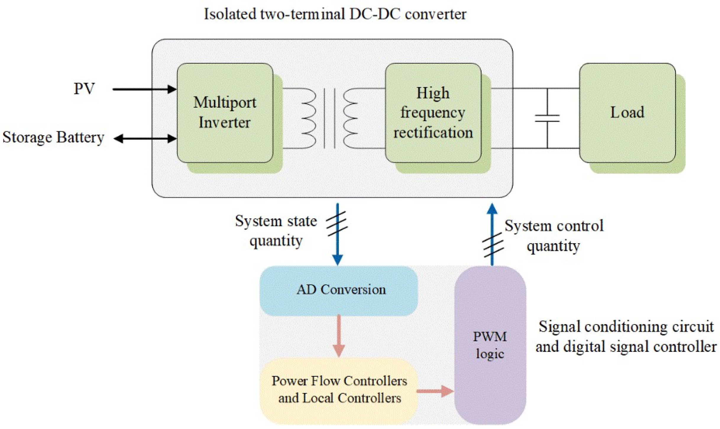
The simulation model was built up in the PSIM environment and simulations of different working modes were carried out. Also, the experiments were carried out based on the experimental setup with the dsPIC33FJ64GS606 digital controller as the control center.
3. System Working State Analysis
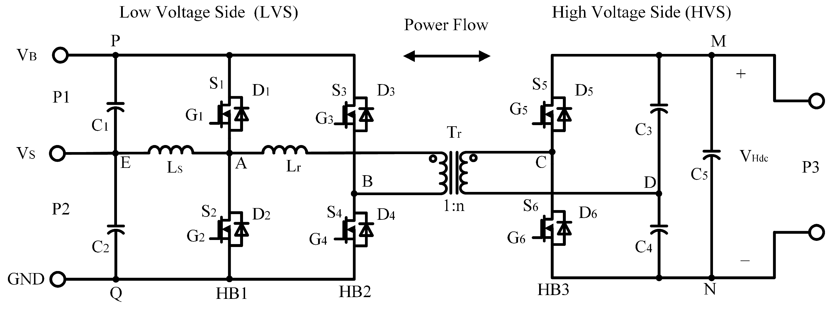
The dual-input buck-boost converter unit is shown in
Figure 3. The topology consists of two input sources (the battery
and the photovoltaic cell
) and an output (the two ends of the bridge arm HB1), which are merged into the low-voltage side DC bus. By controlling the alternate conduction and shutdown of MOS transistor
and MOS transistor
, the battery is charged and discharged. In addition, it provides energy for the low-voltage bus bar.
The output voltage
can be calculated as:
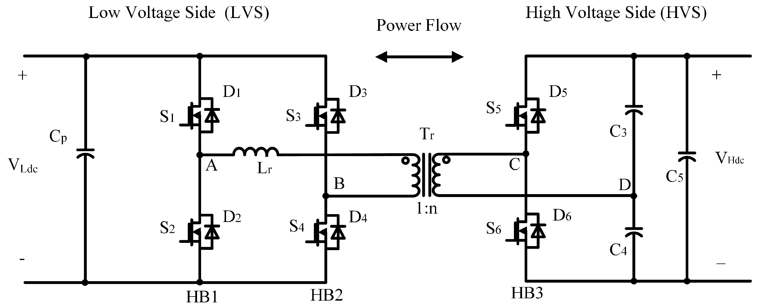
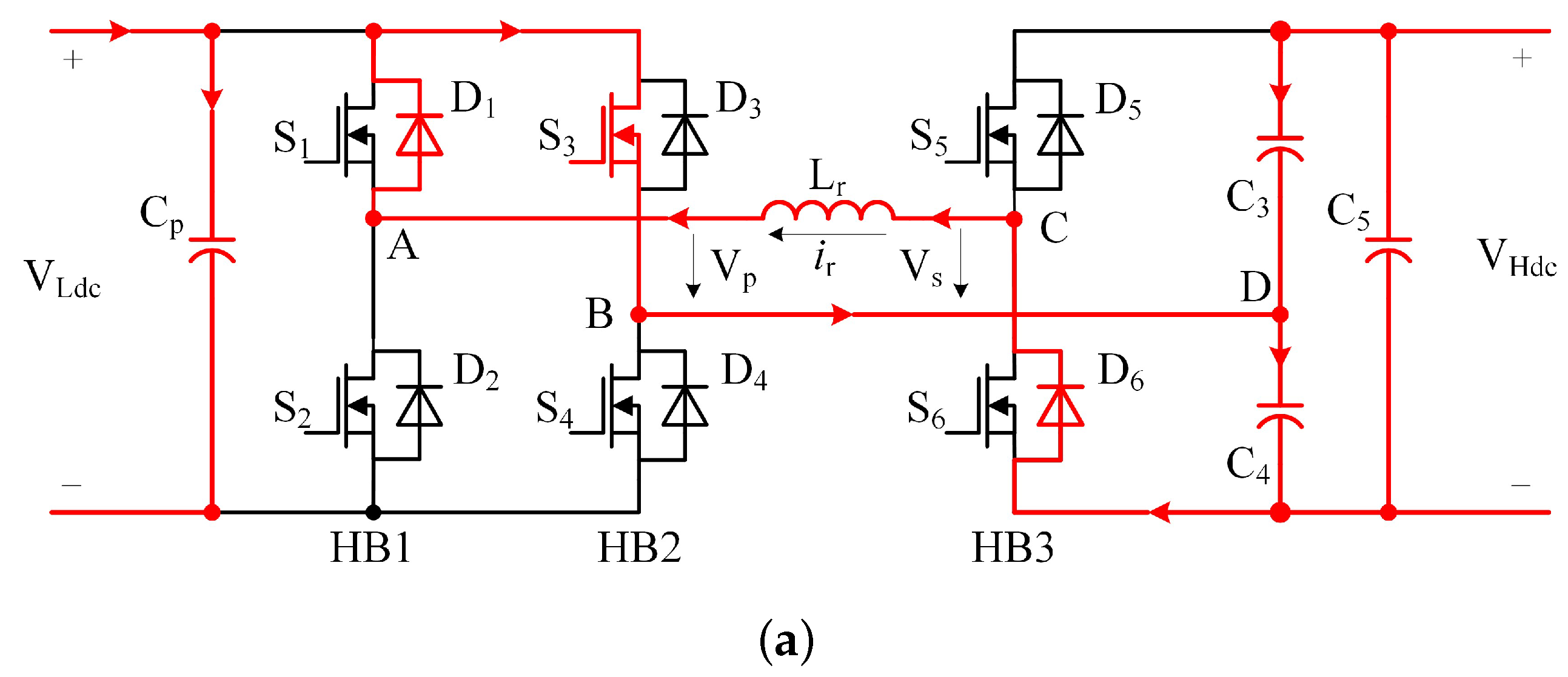
To realize the topology proposed in this article, an asymmetric mixed modulation method is required. The AC voltage square wave signal from the secondary side is converted to the primary side of the transformer to obtain the equivalent circuit shown in
Figure 4, where
is the leakage inductance of the transformer. The AC voltage signals of the primary and secondary sides of the high frequency transformer are
and
, respectively. By controlling the phase relationship between the two AC voltage signals, the magnitude and direction of the transmitted energy can be controlled. When the phase of
is ahead of
, the converter is in the power forward transmission mode at this time. Conversely, the converter is in reverse power transfer mode at this time.
In this proposal, an asymmetric hybrid modulation method is used to make the driving signals of and complementary. The duty cycle of is calculated by the maximum power tracking algorithm, so that the driving signals of and are complementary, and the duty cycle of is the same as that of . The phase shift angle between and is maintained at 180°, so that the driving signals of and are complementary, and the duty cycle is 0.5, that is, = 0.5. Through the hybrid modulation method of duty cycle modulation and phase shift angle modulation (PWM + PSM), a certain phase shift angle is maintained between the driving signals of and .
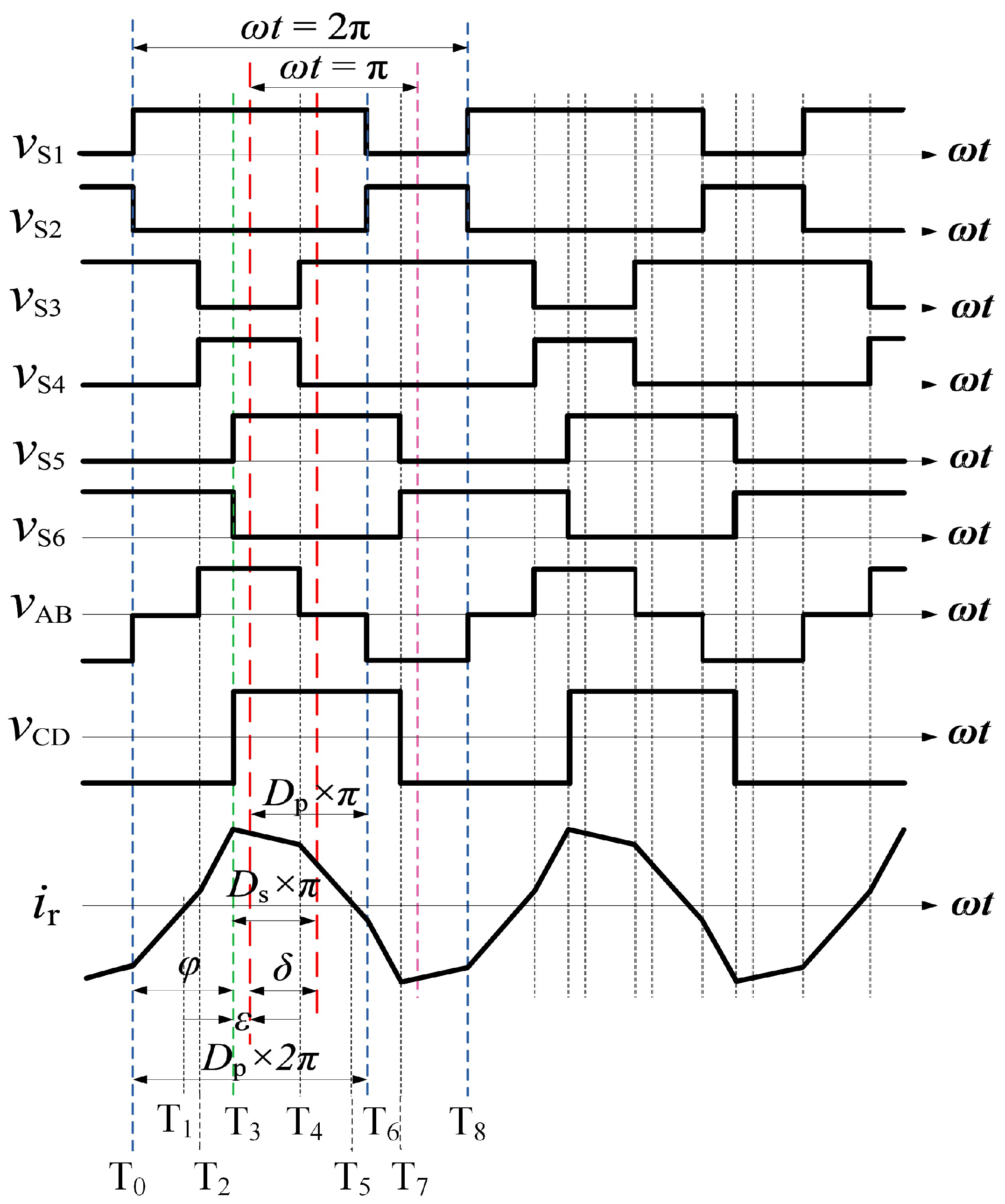
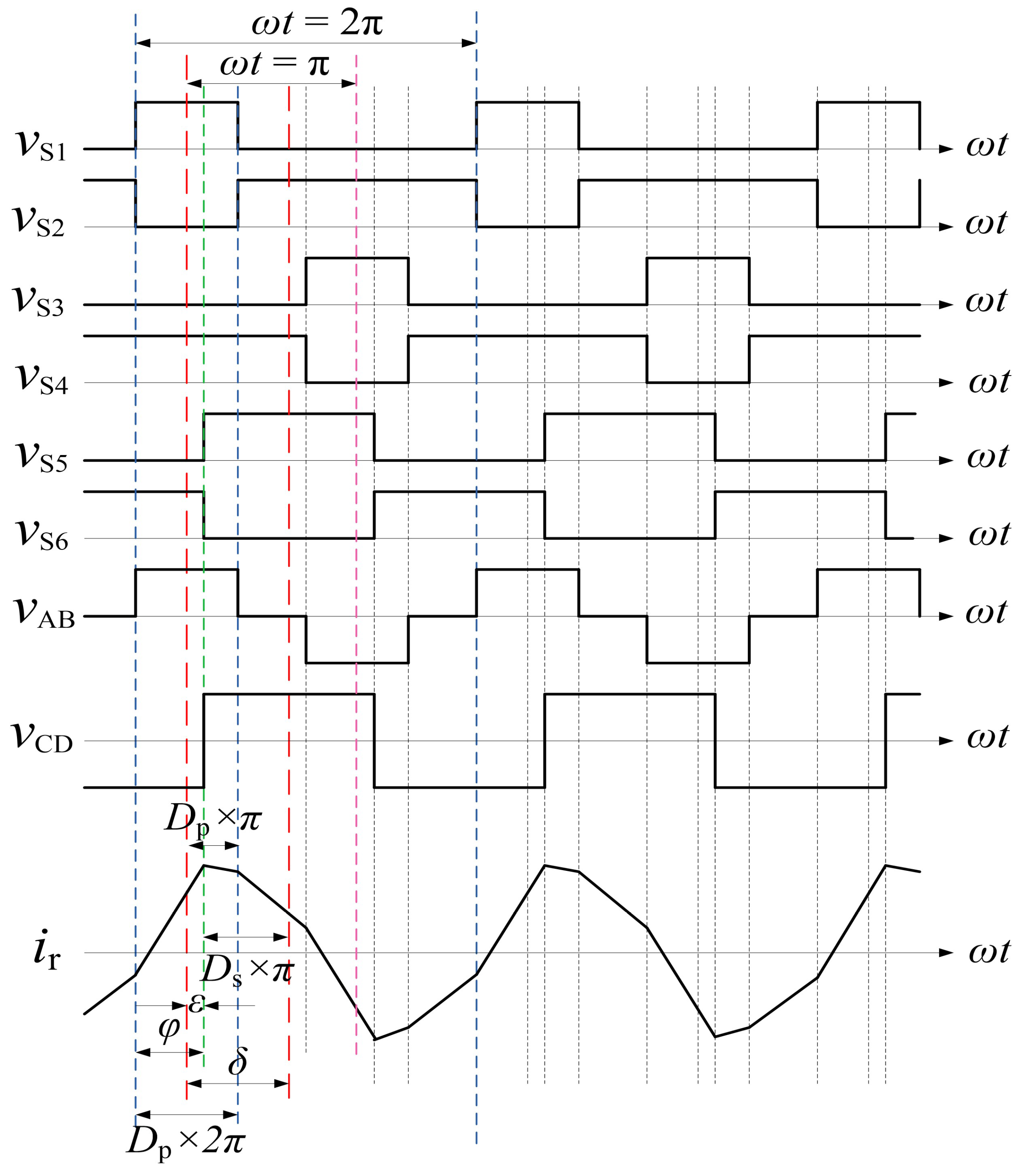
Figure 5 shows the ideal working waveform when the converter is in the power forward transmission mode, and the duty cycle of the primary full bridge is greater than 0.5, where
,
,
,
,
, and
are the voltage waveforms between the gates of
,
,
,
,
, and
, respectively. There is a 180° phase shift between the rising edge of
and the rising edge of
. The
and
are the midpoint voltage of the bridge arm of the primary side inverter and the midpoint voltage of the bridge arm of the secondary side half-bridge fully-controlled rectifier.
is the current flowing through the transformer,
is the duty cycle of
and
, and
is the duty cycle of
, where
= 0.5.
is the center phase shift angle between the high-level midpoint of
and the high-level midpoint of
.
is the shift between the rising edge of
and the rising edge of
phase angle.
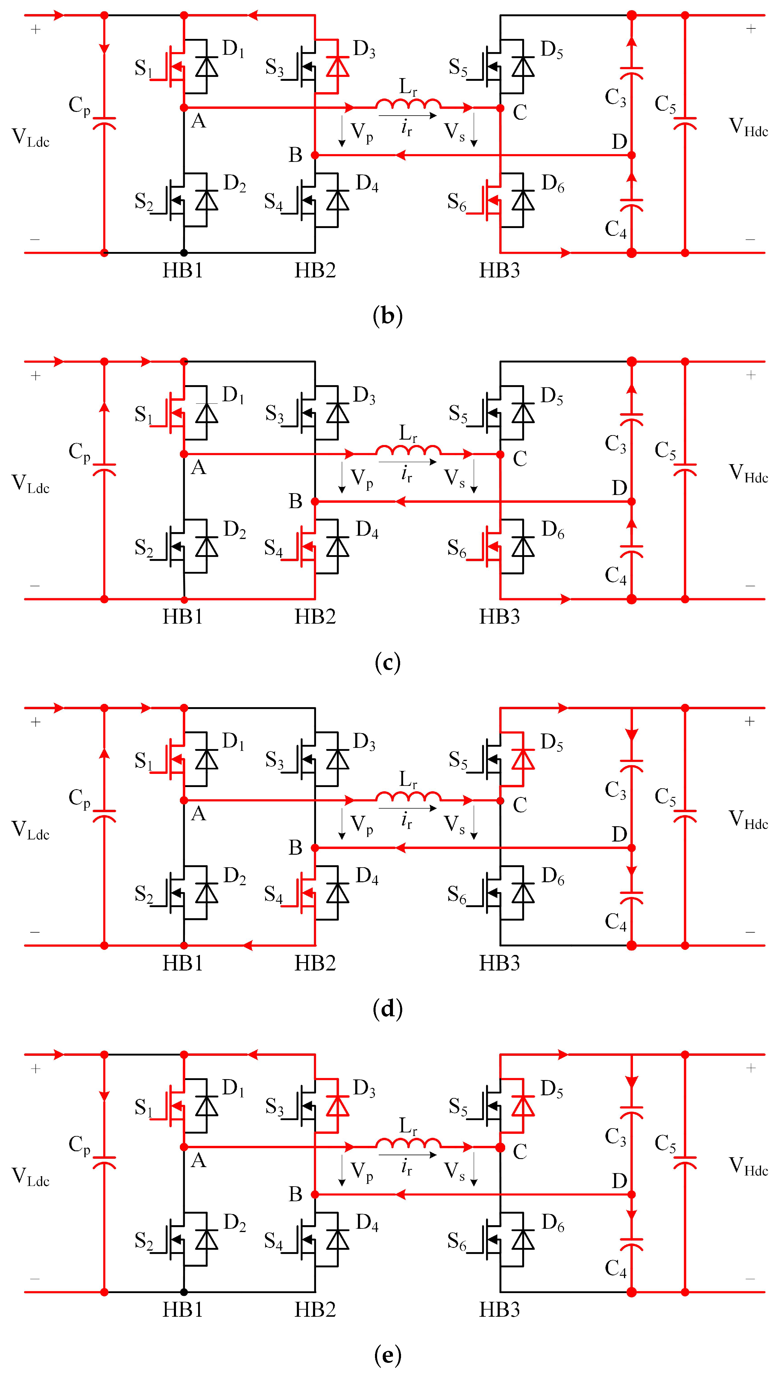
According to the different working states of the switching tubes, each switching cycle is divided into eight stages, and the circuit states of each stage are shown in
Figure 6a–h. The direction of the transformer current
takes the direction marked in
Figure 4 as the positive direction, and the voltage across the inductor is recorded as
, and satisfies
=
−
. The voltages of capacitors
and
are recorded as
and
respectively, and the specified direction is positive and negative. After being converted to the original side, they are recorded as
and
respectively, satisfying
=
/
n,
=
/
n, where
n is the voltage of the transformer turns ratio. Then there is:
State 1 (∼): Trigger a conduction signal to , , and . Since the inductor current is negative, and are both in the off state, is on, and the current flows from , , , , and . However, at this time = 0, = −, = − = > 0, the inductor current increases linearly from a negative value, and the inductor current increases to zero at time .
State 2 (
∼
): The trigger signals of all switch tubes remain unchanged, and the trigger signals of switch tubes
,
and
are still high-level conduction signals. At this time, the inductor current increases to a positive value, and the current changes from
,
, The flow through
,
, and
is changed to flow through
,
,
,
, and
. At this time,
= 0,
= −
,
=
−
=
> 0, and the inductor current increases linearly. At the time of
,
= (2
− 1)
, the total amount of inductive current increase in the interval from
to
is:
State 3 (
∼
): Continue to turn on the signal to
and
, turn off the signal to
, and turn on the signal to
. At this time, the current flows through
,
,
,
, and
,
=
,
= −
,
=
−
=
+
> 0, the inductor current continues to increase linearly. At the time of
,
=
, the total amount of inductive current increase in the interval from
to
is:
State 4 (
∼
): Continue to turn on the signal to the switch tubes
and
, turn off the signal to
, and turn on the signal to
. Since the inductor current is positive, the current flows through
,
,
,
, and
, at this time,
=
,
=
,
=
−
=
−
. At the time of
,
=
, the total amount of increase in the inductor current in the interval from
to
is:
State 5 (∼): Continue to turn on the signal to the switch tubes and , turn off the signal to , and turn on the signal to . Since the inductor current is positive, the current flows through , , , , and , at this time, = 0, = , = − = − < 0, the inductor current decreases linearly, and the inductor current decreases to zero at time .
State 6 (
∼
): The trigger signals of all switch tubes remain unchanged, and the trigger signals of switch tubes
,
, and
are still high-level conduction signals. At this time, the inductor current decreases to a negative value, and the current changes from
,
,
,
, and
flow through
,
,
,
, and
. At this time,
= 0,
=
,
=
−
= −
< 0, and the inductor current continues to decrease linearly. At the moment of
,
= 2
, the total increase of the inductor current in the interval of
∼
is:
State 7 (
∼
): Continue to turn on the signal to the switch tubes
and
, turn off the signal to
, and turn on the signal to
. At this time, the current flows through
,
,
,
, and
,
= −
,
=
,
=
−
= −
−
< 0, the inductor current continues to decrease linearly, at the time of
,
=
, the total increase of the inductor current in the interval from
to
is:
State 8 (
∼
): Continue to turn on the signal to the switch tubes
and
, turn off the signal to
, and turn on the signal to
. At this time, the current flows through
,
,
,
, and
,
= −
,
= −
,
=
−
= −
+
> 0, the inductor current increases linearly, at the moment of
,
= 2
, the total increase of the inductor current in the interval between
and
is:
According to
(0) = −
(
π),
(2
π −
π) = −
(2
Dπ),
(
φ) = −
(
π +
φ), the expression of its initial state can be deduced:
The working waveform of the circuit when the duty ratio
of the primary side is less than 0.5 is shown in
Figure 7. In reverse flow mode, the analysis process is similar to when
is greater than 0.5.
From the waveform analysis in
Figure 5 and
Figure 7, it can be seen that when the duty cycle
> 0.5 and
< 0.5, the relationship between
,
,
,
, and
is:
From the above relationship, it can be concluded that regardless of whether
> 0.5 or
< 0.5, the following is satisfied:
The following formula can be obtained:
Through the above relationship, the phase shift angle between the rising edge of and the rising edge of vs1 can be calculated according to the current primary side duty cycle , secondary side duty cycle , and the central phase shift angle between the high−level midpoint of vs1 and the high-level midpoint of .
The working mode of the proposed system is decided by the energy connection condition of ports P1, P2, and P3, mainly divided into three modes with each mode having a different power flow. Mode I: Both P1 and P2 transfer power to the load P3 through the converter. This mode appears when the power provided by the PV is less than the rated power of the load. In this mode, the battery is in discharging state. Mode II: The PV provides energy to the load (P3) and battery (P2) which means that the power provided by photovoltaics is greater than the rated power of the load, and the remaining energy is charged to the energy storage system. In this mode, the battery is in charging state. Mode III: This mode is the energy feedback mode from the load, thus, both PV and load transfer the energy to the storage battery. In this mode, the battery moves from the discharging state to the charging state.
4. Control Strategy
In order to realize the MPPT control of the PV port and the converted power with direction control, a pulse with modulation and a phase shift (PWM + PSM) control strategy is applied for controlling the proposed conversion system, as shown in
Figure 8, where the PWM duty
is used for MPPT control and the phase shift
is used for power control through PI controller
.
The system control process of hybrid modulation using duty cycle modulation and phase shift modulation can be divided into two parts. One is the duty cycle modulation process, that is, the photovoltaic MPPT algorithm. The other is the phase shift angle modulation process, that is, the output voltage control.
Photovoltaic maximum power point tracking (MPPT) implementation method: the duty cycle disturbance observation method is adopted on the primary side, and it is sent to the dsPIC33F microcontroller after sampling through the photovoltaic cell voltage and current sampling circuit. The dsPIC33F microcontroller will calculate the power according to the current sampled photovoltaic cell voltage and current, and obtain the current photovoltaic cell output power, compare it with the power at the previous moment, and make the current working point move to the maximum power point by disturbing the duty cycle of the primary full-bridge inverter. In this way, the photovoltaic maximum power tracking (MPPT) is realized, and the duty cycle of the primary full−bridge inverter is obtained at the current maximum power.
Closed-loop control process of output voltage on the high side: the output voltage of the secondary side half-bridge full controlled rectifier is sampled, and the output voltage is sent to the voltage controller after comparing it with the target value of the output voltage. The output of the voltage controller is sent to the duty cycle/phase shift angle modulator, and the duty cycle/phase-shift angle modulator is combined with the duty cycle of the current primary side full-bridge inverter and the duty cycle of the secondary side half-bridge full controlled rectifier to calculate the phase-shift angle between the rising edge of the modulation signal of the half-bridge full controlled rectifier relative to the rising edge of the primary-side modulation signal . The amplitude of the output voltage and the magnitude and direction of the transmission power are controlled by adjusting the phase-shift angle.
Calculate the phase shift angle
between the rising edges according to the primary duty cycle
, the secondary duty cycle
, and the central phase shift angle
. Convert
to the corresponding
. The conversion formula is as in (14).
By adjusting the duty ratio of the dual-input inverter on the primary side, the maximum power tracking of the input photovoltaic and the function of the dual-input inverter are realized. Meanwhile, the phase shift angle is adjusted to realize output voltage stabilization and control of the transferred power as well as its flow direction.
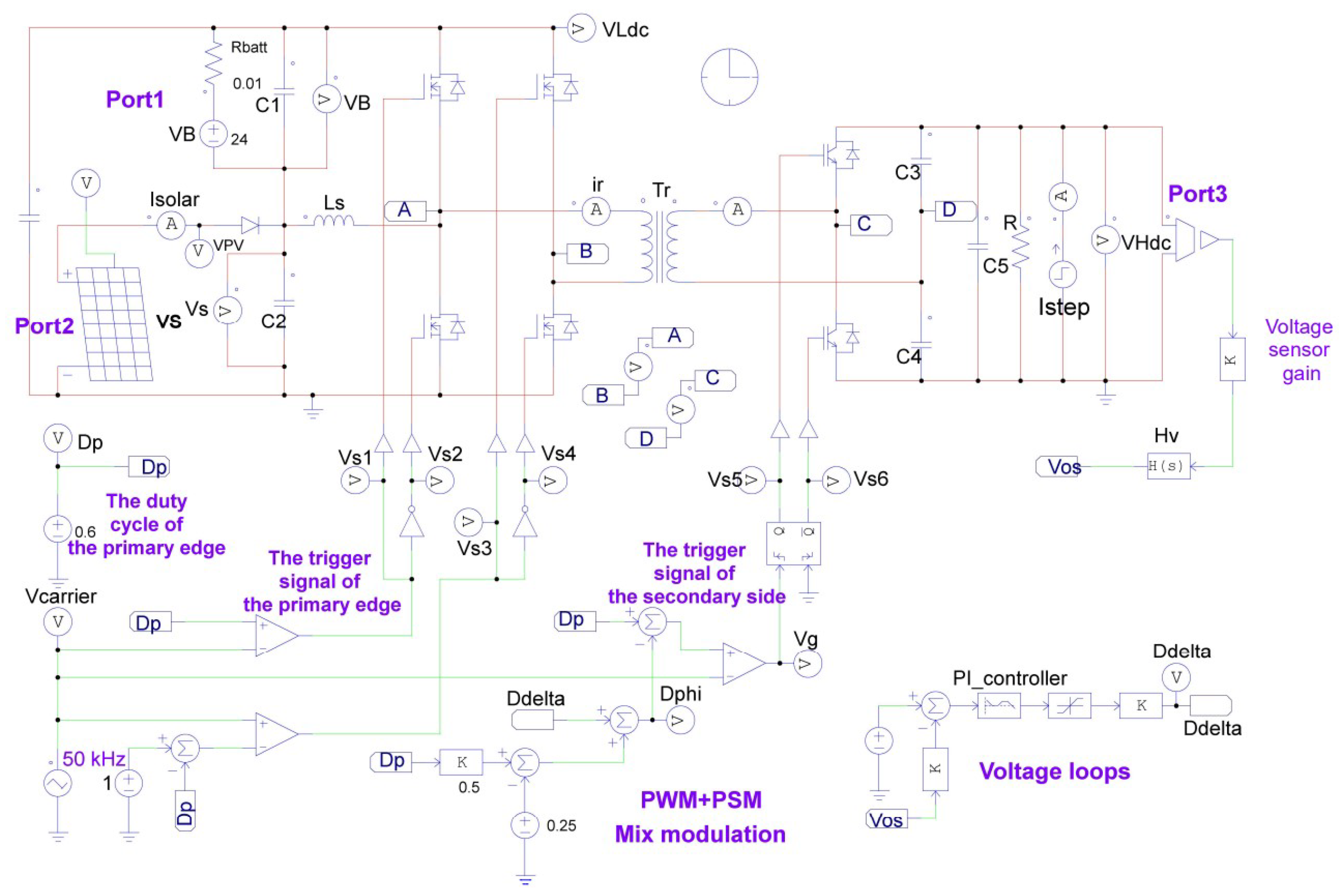
System Simulation and Analysis
In order to verify the working mode and control strategy of the system, a closed-loop simulation of the step-up multiport converter (MPC) proposed in this paper is carried out in the PISM software (9.14 Professional), and the simulation circuit diagram is shown in
Figure 9.
As shown in
Figure 9, the circuit simulation schematic consists of two parts: The main circuit part and the control circuit part. The main circuit mainly includes two input sources,
and
, access port 1 and port 2 respectively, a full-bridge inverter, a transformer, a half-bridge rectifier, a voltage regulator capacitor, and load.
The control circuit mainly includes a reference carrier signal, a voltage sampling circuit, a voltage control circuit, a PWM + PSM hybrid modulation circuit, a primary-side trigger signal generation circuit, and a secondary-side trigger signal generation circuit. The is the first-order low-pass filter transfer function; The PI controller in the voltage control loop is a PI algorithm controller with two poles and two zeros; and are and , respectively, which appear in the previous sections; is the primary duty cycle.
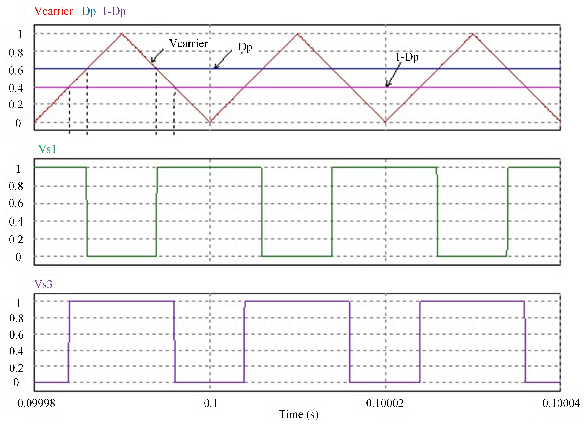
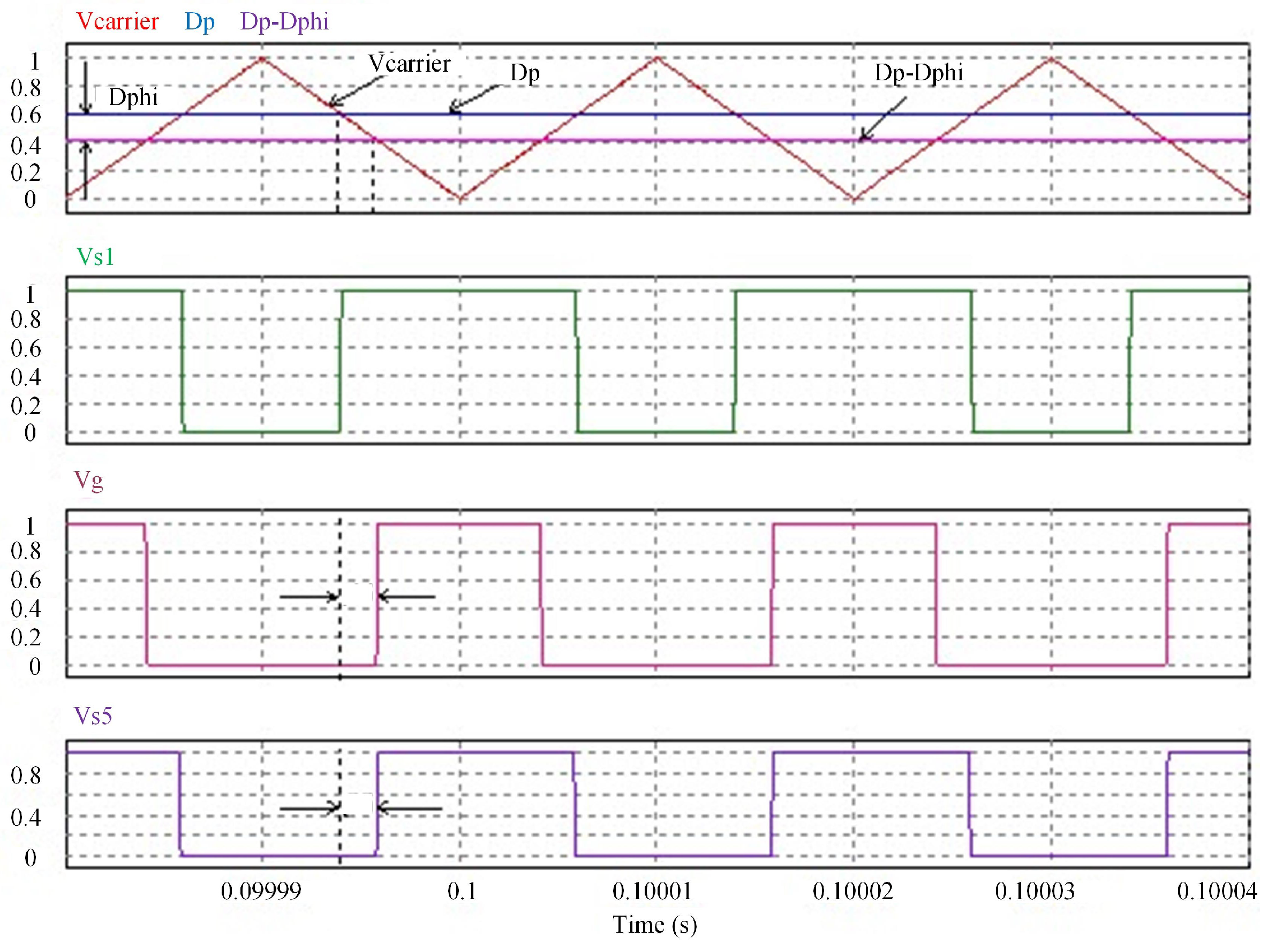
The principle of trigger signal generation of the primary and secondary sides is simulated and verified in PSIM. The primary side duty cycle is given as
= 0.6 and
= 0.1 (
= 0.2
) for simulation, and the waveform generated by the primary trigger signal is shown in
Figure 10. The waveform generated by the secondary trigger signal is shown in
Figure 11. The simulation results are consistent with the previous analysis and verify the feasibility.
Table 1 shows the circuit simulation parameter settings.
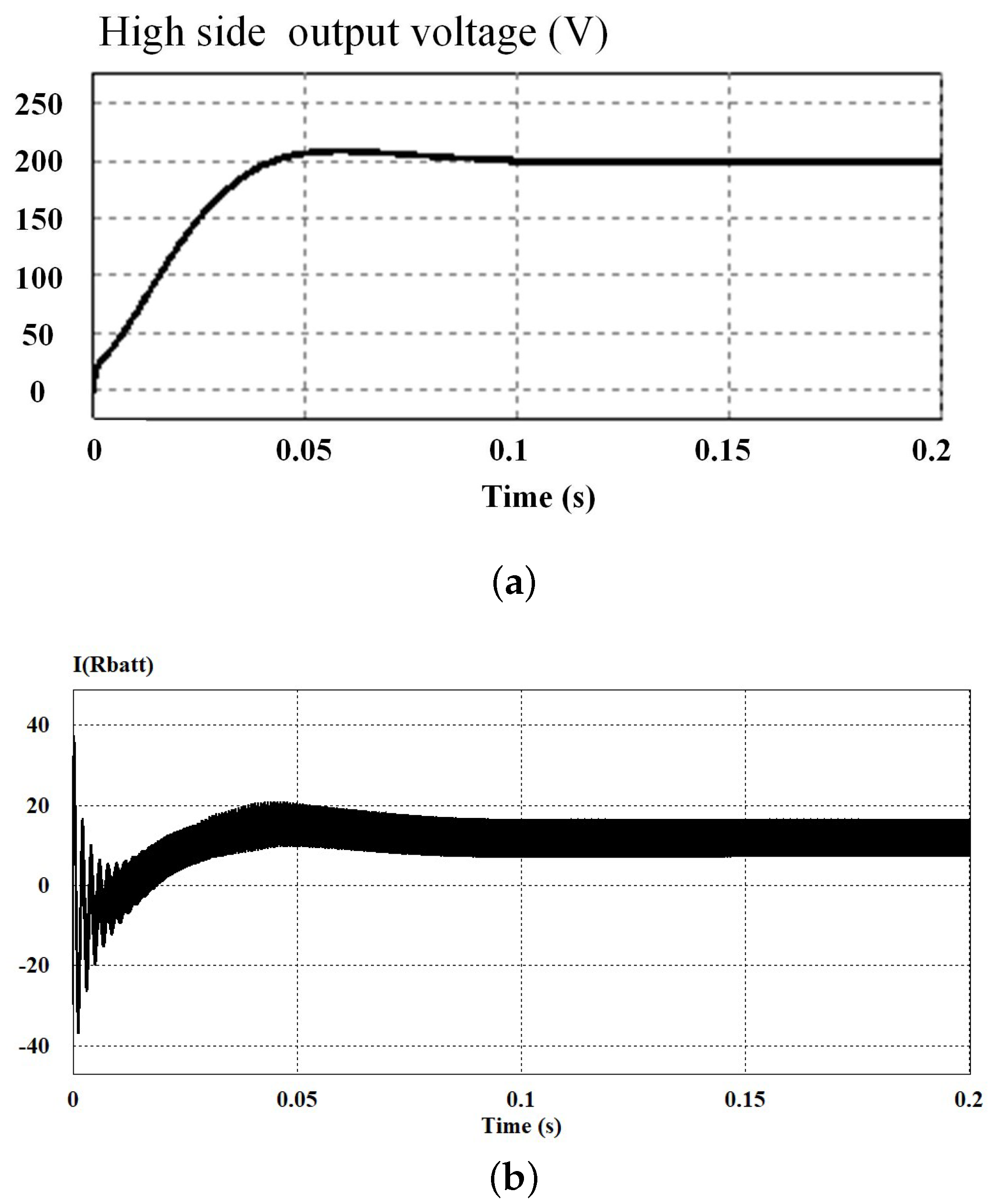
In this state, the step current source is set to an invalid state, the output voltage of the control high-voltage side is 200 V, and the load is a resistive load. At this time, the photovoltaic cell works at the maximum power point, and the photovoltaic provides 200 W of power, and it can be seen that the output power of the photovoltaic cell is less than the power required by the load, and the combined power supply of the battery is required to meet the power demand of the load side.
Figure 12 shows the simulated waveform of the output voltage of the high voltage side. As can be seen from the simulation results, the final output voltage is stabilized at 200V and the output voltage on the high side is effectively controlled. The battery current is positive, which proves that the battery is in a discharged state.
5. Expiremental Verification
Based on the theoretical analysis and simulation verification result, an experimental prototype was established using the dsPIC33FJ64GS606 the as digital controller. The device is mainly composed of a main circuit, a control circuit, and an auxiliary power circuit. The control circuit includes a chip and its peripheral circuits, a sampling circuit, and a driving circuit. The experimental platform is shown in
Figure 13.
Table 2 shows the circuit experimental parameters.
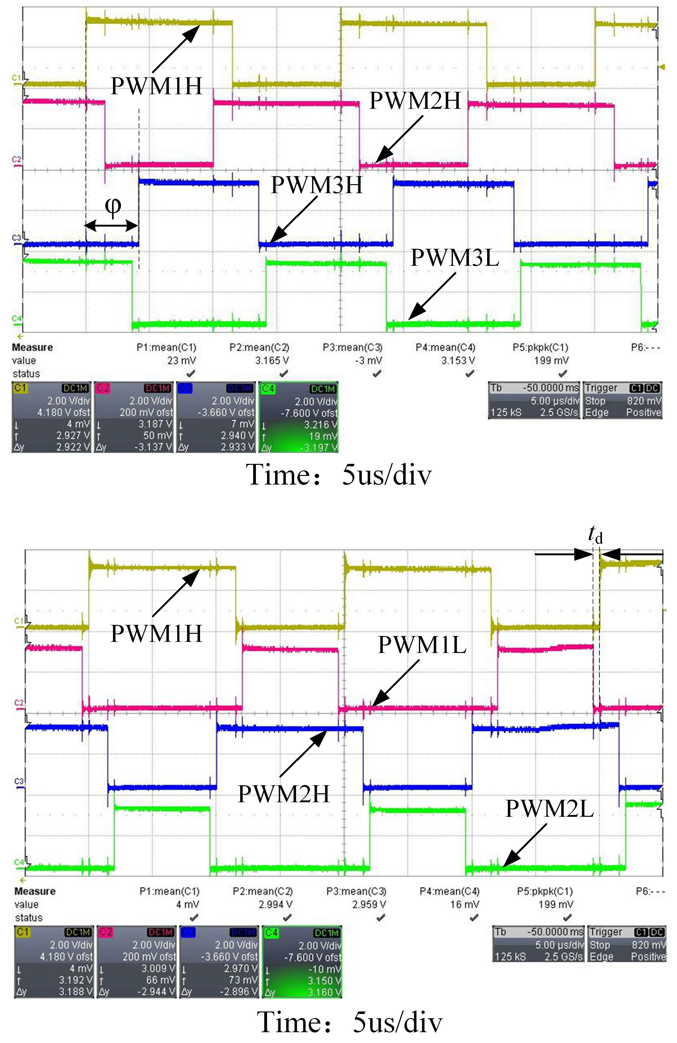
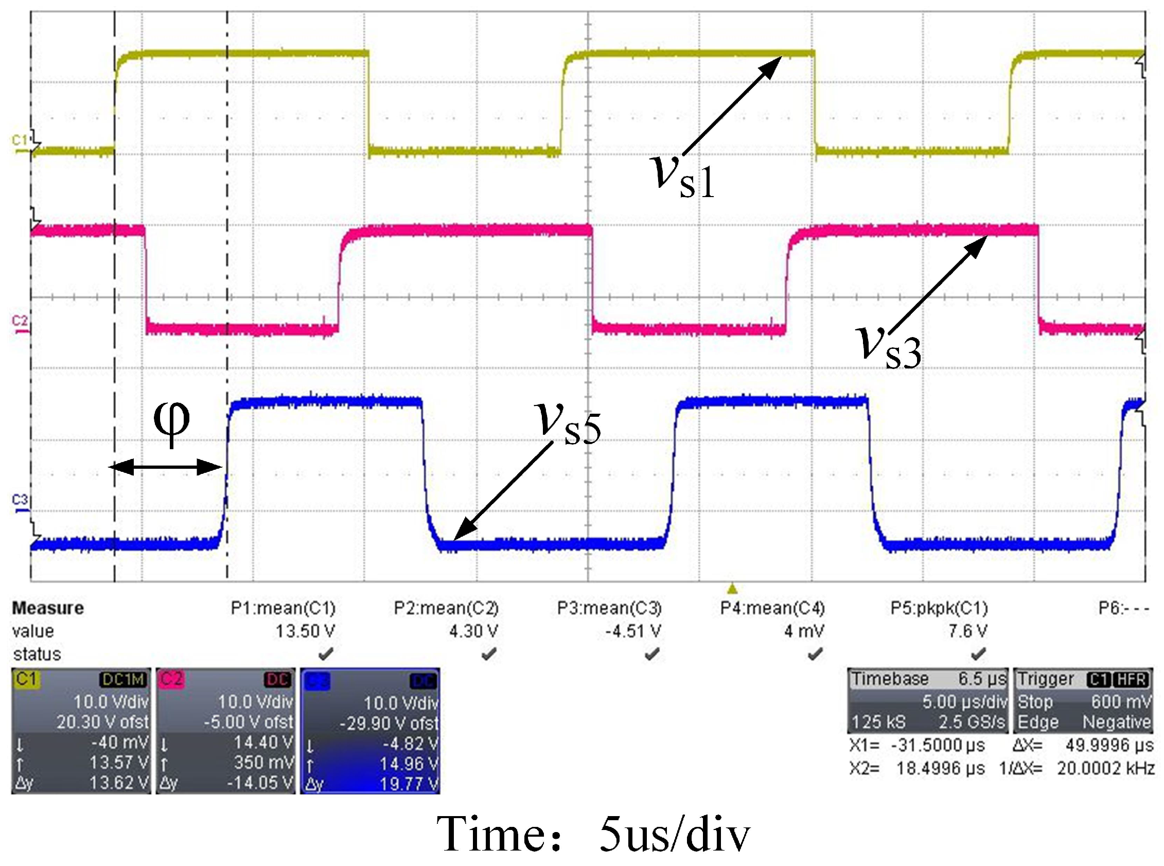
The PWM trigger signal generation of the primary and secondary side is experimentally verified, and the duty cycle of the primary side is given as 0.6, the duty cycle of the secondary side is 0.5, the dead time
= 0.5 us, the phase shift angle
= 0.4
(the corresponding central phase shift angle
= 0.3
), and the corresponding waveform is obtained, as shown in
Figure 14.
As shown in
Figure 15 (all four channels are 2 V/div), the PWM signal waveform with a frequency of 50 kHz output by the PWM module pin of dsPIC, in which the phase shift angle between the rising edges of the two waveforms of PWM1H and PWM3H is
, is consistent with the set value requirements, and the PWM and phase shift operations can be completed without consuming any DSP resources.
Figure 16 shows the corresponding gate-to-source trigger signal waveform (10 V/div for all three channels) after the PWM signal output by the PWM module is passed through the drive circuit.The figure shows the waveforms of the gate trigger voltages
,
and
obtained by PWM1H, PWM2H, and PWM3H after the corresponding drive circuits, and the phase shift angle between the rising edges of the waveforms of
and
is
.
As can be seen from
Figure 16, the voltage of
and
is 0–13.5 V, which meets the output requirements of the IR2110S and meets the opening and closing voltage requirements of the primary side MOS tube; the voltage of
is −5–+15 V, which meets the output requirements of KD301L, and also meets the opening and closing voltage requirements of the secondary side MOS tube.
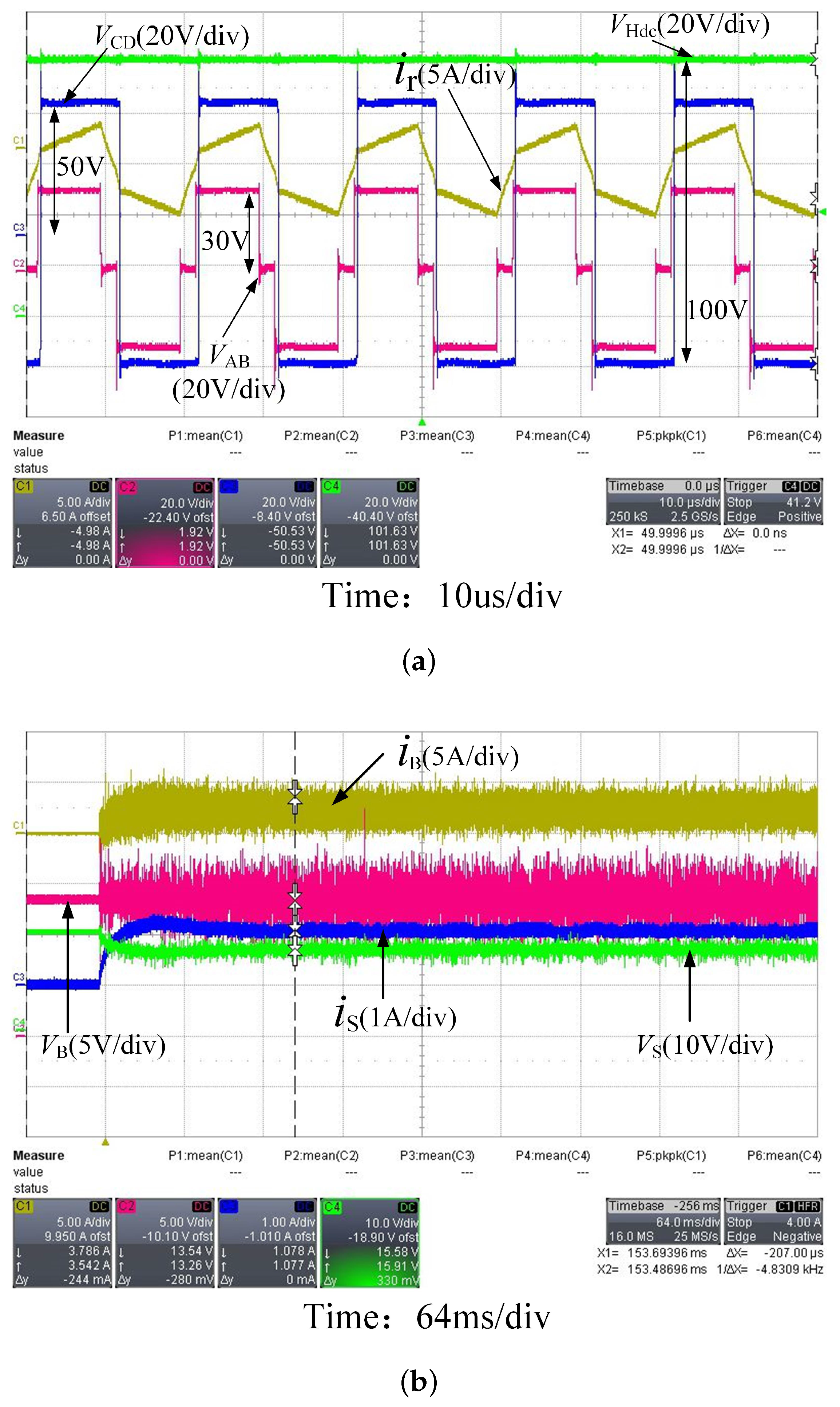
In the experiment, a series combination of a DC power supply and a resistor is used to simulate photovoltaic cell access P2. P1 is connected to a 12.5 V battery and P2 is connected to a 22 V voltage source to simulate the PV panel. The output port P3 is connected to the load which is represented by a 160 ohm resistor. The duty cycle
of the LVS is set to 0.6, and the controlled output voltage is set to 100 V. The experimental results of the steady-state are shown in
Figure 15.
From the steady-state experimental results shown in
Figure 15a, the HVS output voltage
of 100 V has been successfully controlled. From the waveforms of voltage
and voltage
, it can be seen that the high-level center of
is ahead of the high−level midpoint of
, that is, the phase of the primary side is ahead of the secondary side, the primary side of the transformer transmits power to the secondary side, and the system is in the power forward transmission state.
The battery current shown in
Figure 15b is positive at about 3 A, thus, the battery is working under discharging mode. The experimental results are in line with the theoretical analysis and simulation, and the control system effectiveness has been successfully verified.


