1. Introduction
The solid-state transformer (SST) is becoming an important technology and is foundational to applications that include traction systems, offshore energy generation, DC grids and especially microgrids. Its advantages, such as accurate output-voltage regulation, short-circuit current limitation, power factor compensation, reduced weight and volume in comparison with traditional transformers, and voltage-dip immunity under certain limitations, enable the construction of a new paradigm in electric power systems [
1].
The future of the electric power system seems to be a smart grid with power-flow management, incorporated energy storage systems, quick transient response and high integration of renewable energy [
2]. All of these features can be incorporated through the utilization of SST. However, this device still has opportunities for improvement, mainly related to cost reduction, reliability, and efficiency [
3].
The usual topology of the SST is presented in
Figure 1. It shows the AC-DC conversion (Stage 1), DC-DC conversion (Stage 2), and DC-AC conversion (Stage 3), with the high-voltage utility grid on the left and the low-voltage microgrid on the right and all stages allowing bidirectional power flow. Stage 2 traditionally employs a DC-DC converter through a resonant magnetic link to connect high-voltage DC to low-voltage DC, and the efficiency of SST is closely related to losses in this stage.
The dual active bridge (DAB) is the general term for the isolated converter formed by the union of two active bridges through an inductor and a high-frequency transformer.
The requirements for building a DAB controller are a fast transient response, minimum steady-state error and reduced losses on the power converter. Hence, an adaptive model predictive control (AMPC) is proposed for a DAB converter in this work. The topology adopted in this work is shown in
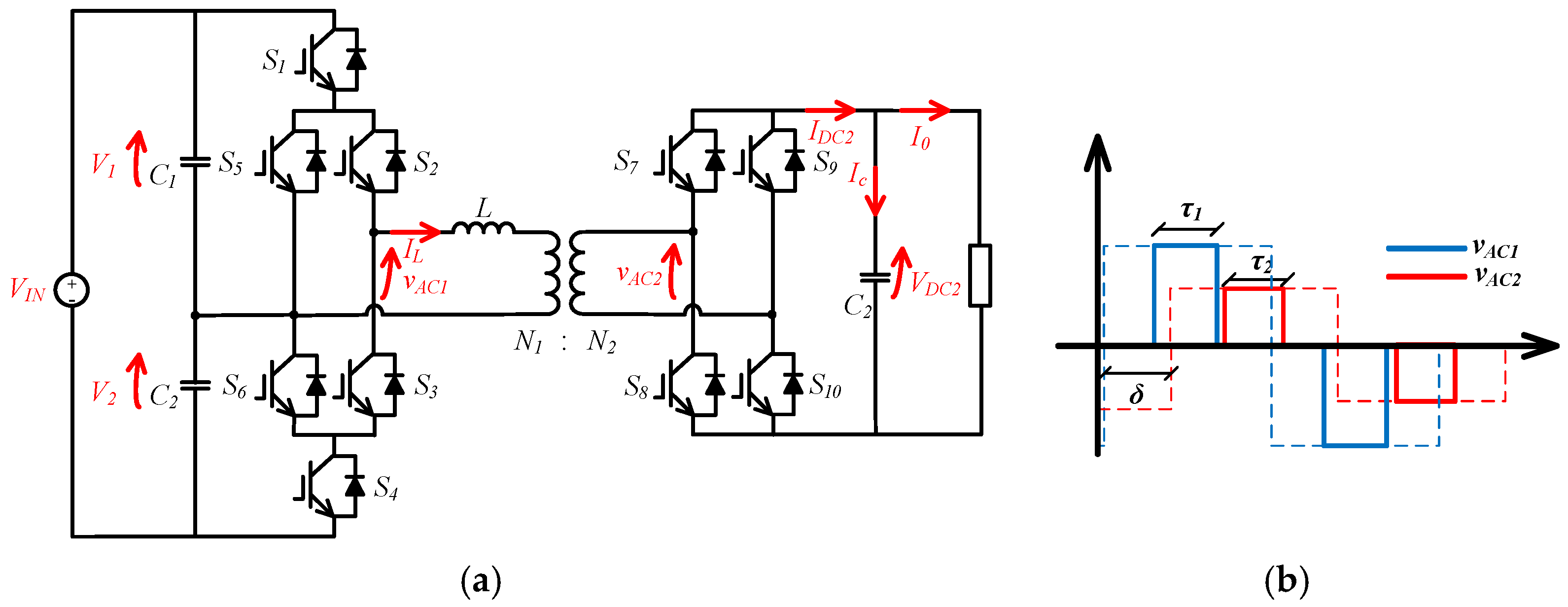
Figure 2 and operates with an active neutral point clamped (ANPC) converter on the high-voltage side and a H-bridge on the low-voltage side. In this work, it is referred to as ANPC-DAB. Its performance is evaluated through a
prototype.
1.1. Literature Review
1.1.1. DAB Converter Topology
The H-bridge two-level DAB is the most commonly used topology for Stage 2 of an SST. Despite the many advantages of this structure, it is unable to deal with high power and high voltage, being limited by semiconductor technology.
The main solution to this difficulty is the series and parallel connection of the converters; however, additional challenges arise in equalizing voltages and sharing currents. Another alternative is the cascade connection of multiple DAB converters, which increases the number of power switches and the complexity of the control scheme. Hence, the utilization of multilevel structures seems to be the best solution. Many multilevel structures have been widely used with success. Various three-level (3L) topologies have been applied to the DAB converter: flying capacitor, neutral point clamped (NPC), and ANPC [
4].
The NPC topology is still widely employed in the industrial sector, notably for operating medium-voltage electric motors [
5]. However, the 3L-NPC has some limitations that affect its performance. Some of the switches must withstand higher voltages than others [
6], and the power loss in each semiconductor is highly unbalanced [
6].
The ANPC converter was proposed to overcome these problems by replacing the clamping diodes with active switches generating redundant switching stages [
7]. These redundant stages are used to equalize the voltage and reduce unbalanced losses in each switch, increasing the power-processing capacity of the converter.
1.1.2. Modulation Techniques for Loss Reduction
Traditionally, the single-phase shift (SPS) modulation is used in DAB converters. The main advantage of this strategy is that it allows for zero voltage switching (ZVS) over a wide operating range [
8]. However, when the relationship between the input and output voltage is far from unity, especially under small loads, these soft-switching techniques are not possible. Additionally, the converter experiences significant backflow-power in this scenario, leading to high circulating currents and increased stress on the switches and conduction losses. In conclusion, the SPS modulation may not ensure high efficiency of the DAB converter over its entire operating range.
A previous work has shown the improvements obtained through the utilization of trapezoidal and triangular modulation techniques [
9,
10]. These techniques can naturally extend the DAB’s soft-switching operation and consist of the utilization of pulse widths different from 50% [
11]. Their proper application can increase the number of soft commutations to four (for trapezoidal modulation) or six (for triangular modulation) out of a total of eight in a cycle, even during operation with reduced loads.
In the AC-DC conversion literature, various balancing control strategies have been proposed to optimize the loss distribution of the ANPC circuit [
7,
12,
13]. The voltage synthesized by the rectifier takes on
(
) or zero (
) during the positive cycle of the electrical grid, resulting in
type commutations for half of the grid period. During the negative cycle of the electrical grid, the voltage synthesized by the rectifier takes on
(
) or zero (
), resulting in
type commutations for the other half of the grid period. However, in the case of the DAB converter, the ANPC bridge losses distribution is carried out at each sampling time, with
switches occurring within each sampling period. As a result, all six switches are used within each switching period of the DAB converter.
The literature includes studies on ANPC-DAB switching for loss distribution among the converter switches. Some states involving the transition between the current path through the clamping diode and through the active switch of the converter are presented in [
4]. In [
14], a modulation is proposed to minimize the number of switching actions, realizing the ZVS turn-ON for all switches and avoiding hard switching turn-OFF in specific switches. In [
15], the electromagnetic interference (EMI) caused by zero voltage switching in the ANPC-DAB converter was evaluated.
1.2. Contributions
The literature review revealed that work on DAB converters can be divided into two groups. The first group involves the development of modulation strategies to enhance the efficiency of the power converter, while the second group deals with novel control techniques to improve the transient and steady-state response. In this paper, both goals are pursued simultaneously through a novel scheme pf control and modulation.
The control proposal was developed to manage the DAB converter and is based on model predictive control (MPC), which incorporates a variable phase-shift adjustment depending on the error between the desired value and the measured variable. However, it has been enhanced for AMPC control. In this new configuration, the control is capable of selecting operation modes (trapezoidal and triangular) in order to minimize losses and thus enhance converter efficiency. The proposed AMPC is applied to an ANPC-DAB, and the results are validated through an experimental setup.
Going beyond previously published work found in the literature, this analysis includes the following: the utilization of a realistic switching frequency (); a compensation scheme for the AMPC delay; tests with load disturbance rejection; an improved cost function that considers capacitor discharge; and a quantitative study of the influence of parameter variation.
1.3. Paper Organization
The paper is organized as follows:
Section 2 presents the mathematical modeling of the SPS and the triangular and trapezoidal modulations. The proposed control scheme is detailed in
Section 3.
Section 4 shows the results of the computational simulation. The experimental results are shown and discussed in
Section 5. Finally,
Section 6 shows the conclusions of this work.
2. ANPC-DAB Topology and Modulations
The DAB converter is formed by two active bridges connected through a high-frequency transformer. In this study, an ANPC converter is used on the high-voltage side, operating as an inverter. There is an H-bridge on the low-voltage side, operating as a rectifier. Together, they form the ANPC-DAB topology, as shown in
Figure 2a.
Figure 2b shows a generic representation of the three-level voltages
and
synthesized by the active bridges using a centralized PWM. The dashed line represents the voltage generated by SPS modulation. The phase shift
and inner phase shift
and
are defined in Equation (1):
One of the fundamental characteristics of the DAB converter is its ability to operate with ZVS in a large part of its operating range when operating in SPS modulation [
8,
16], and this ability can be extended to the entire operating range when using modulations with greater degrees of freedom [
17,
18].
The ZVS conditions of the ANPC-DAB are consistent with the ZVS conditions of a dual H-bridge DAB [
4,
14]. Thus, when they use the same phase-angle shift modulation method, the ANPC-DAB, DNPC-DAB, and H-bridge DAB circuits have the same phase-shift ranges for the ZVS of all switches [
19].
The next section analyzes the switching used in the ANPC-DAB converter.
Section 2.2 contains an analysis of the operating points at which the ZVS occurs in the SPS modulation.
Section 2.3 contains an analysis of the ZVS involving triangular and trapezoidal modulations, the basis of AMPC.
2.1. ANPC-DAB State Switching
The 3L-ANPC topology has one active switch connected in parallel with each clamp diode. These two switches allow the AC terminal to be connected to the midpoint DC link (neutral point) in more than one switching state. The four resultant zero states are presented in
Table 1 and described as
,
,
, and
. This configuration allows for a more even distribution of switch losses in the converter, increasing its energy-processing capacity.
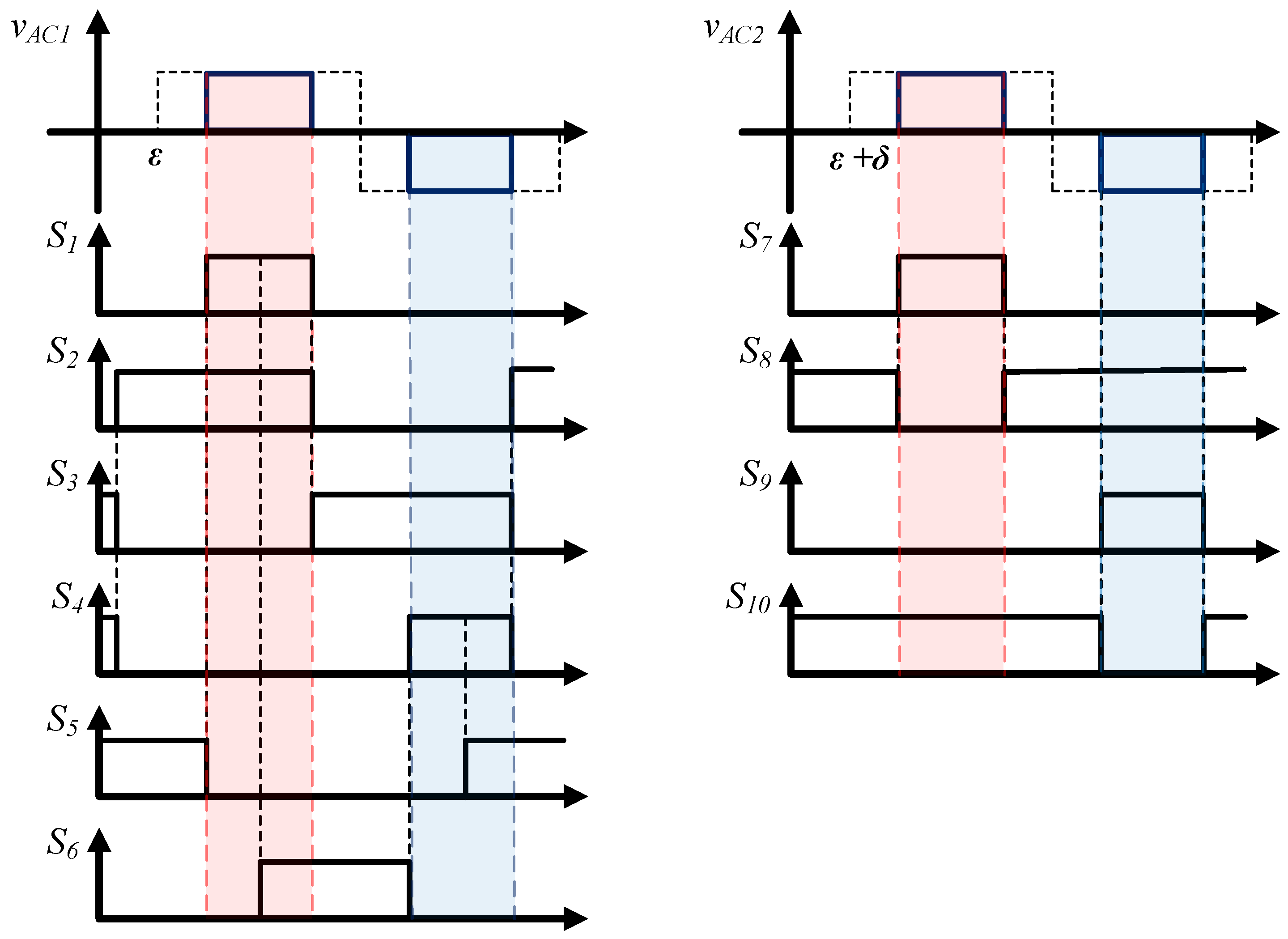
The switching scheme used in this work is shown in
Figure 3. The
and
voltage synthesized and the trigger pulses on the switches for both sides of converter are own, highlighting the positive cycle in red and the negative cycle in blue.
2.2. SPS Modulation
SPS modulation is the main modulation used by the ANPC-DAB converter. The only control variable is the phase shift, that is,
. In this work, the voltages on the ANPC-DAB input capacitors will be the same, that is,
. The power transferred using SPS modulation, for a given operating point, is shown in (2).
where
is power transfer inductance;
is the transformer ratio (
);
is the switching frequency of the converter; and
and
are the input and output voltage on capacitors, respectively.
The power boundaries for the ZVS actuation of the primary and secondary active bridges are presented in (3). If the DAB’s power is above
or below
, the DAB converter cannot operate with ZVS [
20].
where
is the rated phase shift.
The DAB transformation ratio
is defined in (4). When
, the DAB operates in ZVS over the whole power range. When
, the primary bridge operates with hard switching. When
, the secondary bridge operates with hard switching.
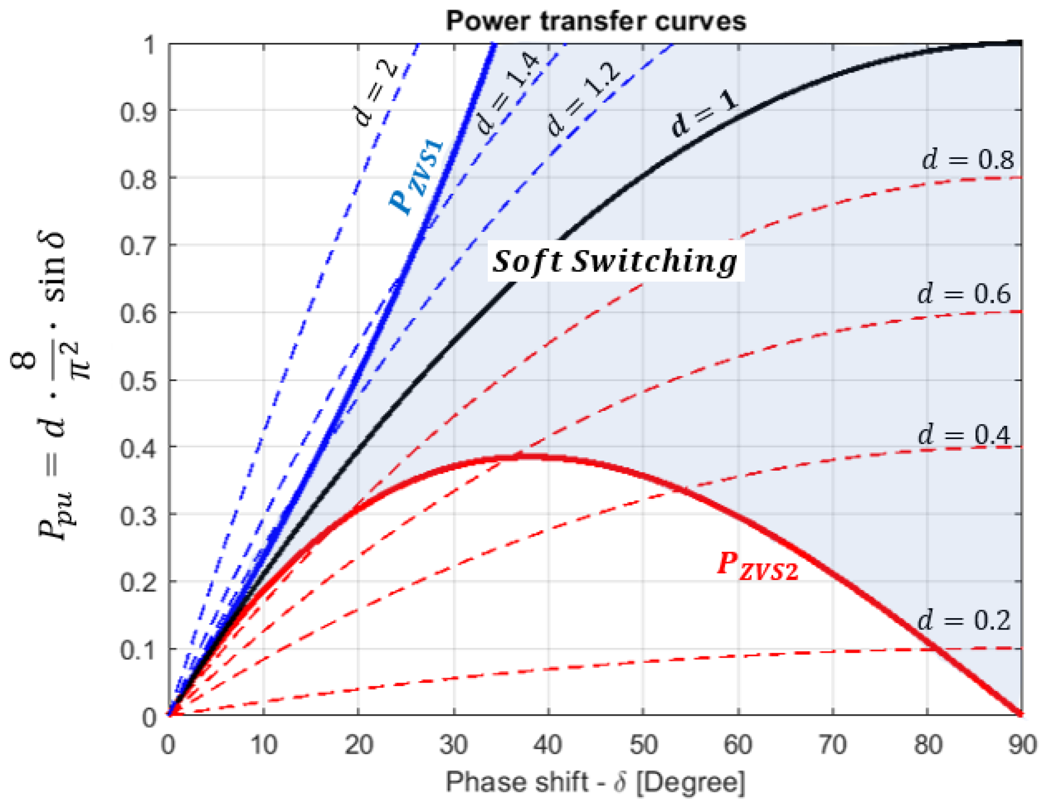
Figure 4 shows the DAB power curve as a function of various values of
to highlight the ZVS region. The solid blue and red lines indicate the power limits within which the primary and secondary bridges, respectively, can operate in soft switching. The solid black line represents
, where the converter operates in soft switching. The dashed lines show the operating points for
. For this analysis, we assumed that
.
These curves show that small phase shifts and significant deviations from unity in the DAB transformation ratio make it difficult to operate the converter in ZVS and decrease its efficiency at those points. Thus, SPS modulation is insufficient to ensure high-efficiency operation of the DAB converter over its entire operational range.
2.3. Triangular and Trapezoidal Modulation
An alternative method by which to extend soft switching to regions where SPS modulation does not allow ZVS operation is to apply triangular and trapezoidal modulation.
Triangular modulation has the advantage of allowing soft switching on six transitions, for a total of eight switchings. However, it cannot be used over the entire operating range of the converter because its power transmission capacity is limited, and it is possible to transfer power only when .
When
, the phase shift
and inner phase shift
and
are calculated so that the current in the inductor
is zero when there are simultaneous changes of state:
in the primary and secondary bridge and
in the secondary bridge. When
, the phase shift
and inner phase shift
and
are calculated so that the current in the inductor
is zero when there are simultaneous changes of state:
in the primary bridge and
in the primary and secondary bridges. In the negative half-cycle, the procedure is repeated, replacing
with
.
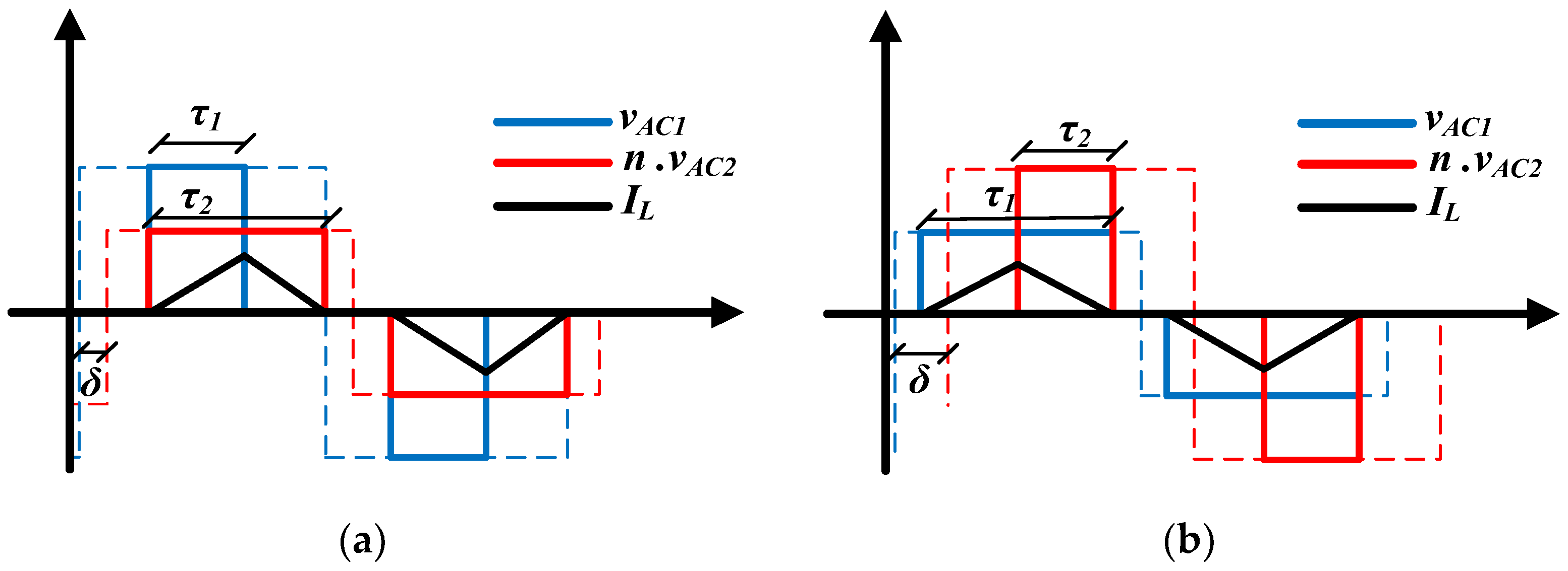
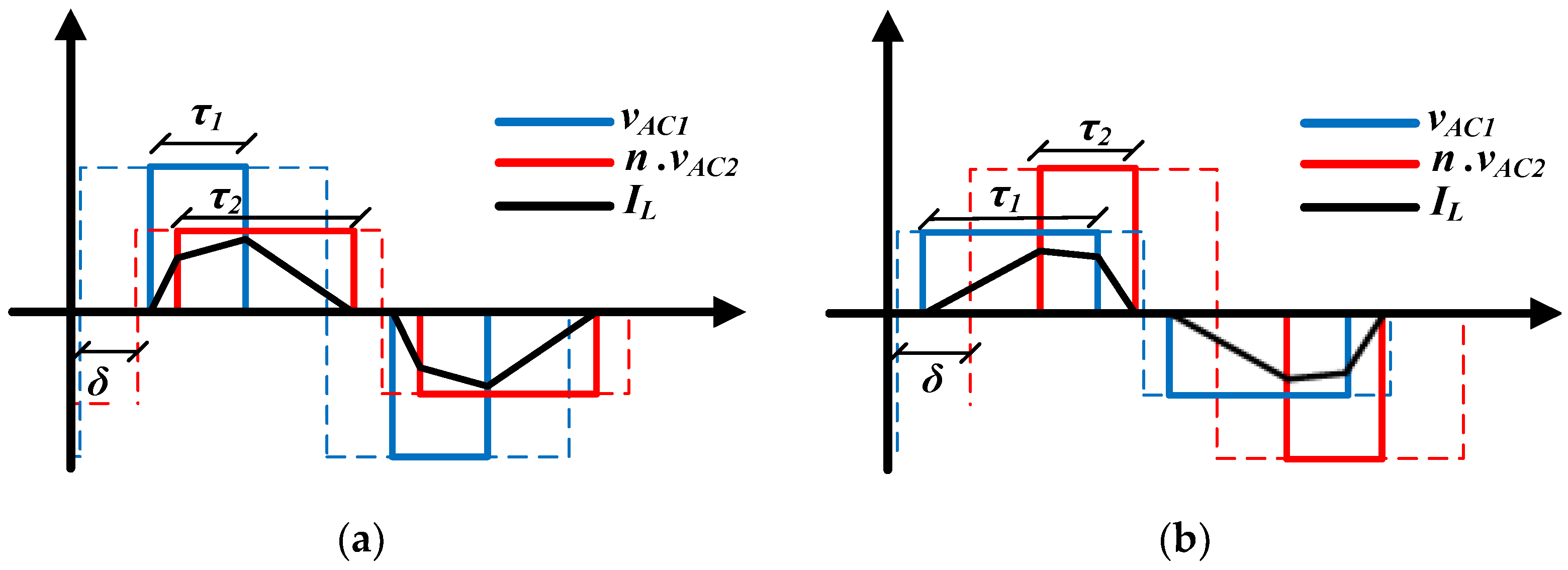
Figure 5 shows the waveforms of the voltages
and
on the active bridges and the inductor current
.
The values of the inner phase shift
and
for the triangular modulation are calculated from the voltages and phase shift. When
, the calculation is done as shown in (5). When
the calculation is done as shown in (6).
When triangular modulation cannot supply the necessary power for a given operating point, trapezoidal modulation is used. Trapezoidal modulation is an extension of triangle modulation, which ensures smooth transition between modulations [
11]. In addition, soft switching occurs in four out of the eight switchings per cycle. Moreover, this modulation is possible for any value of
.
Figure 6 shows the waveforms of the voltages
and
on the active bridges and the inductor current
for the trapezoidal modulation.
The values of the inner phase shift
and
for the trapezoidal modulation are calculated from the voltages and phase shift, as shown in (7).
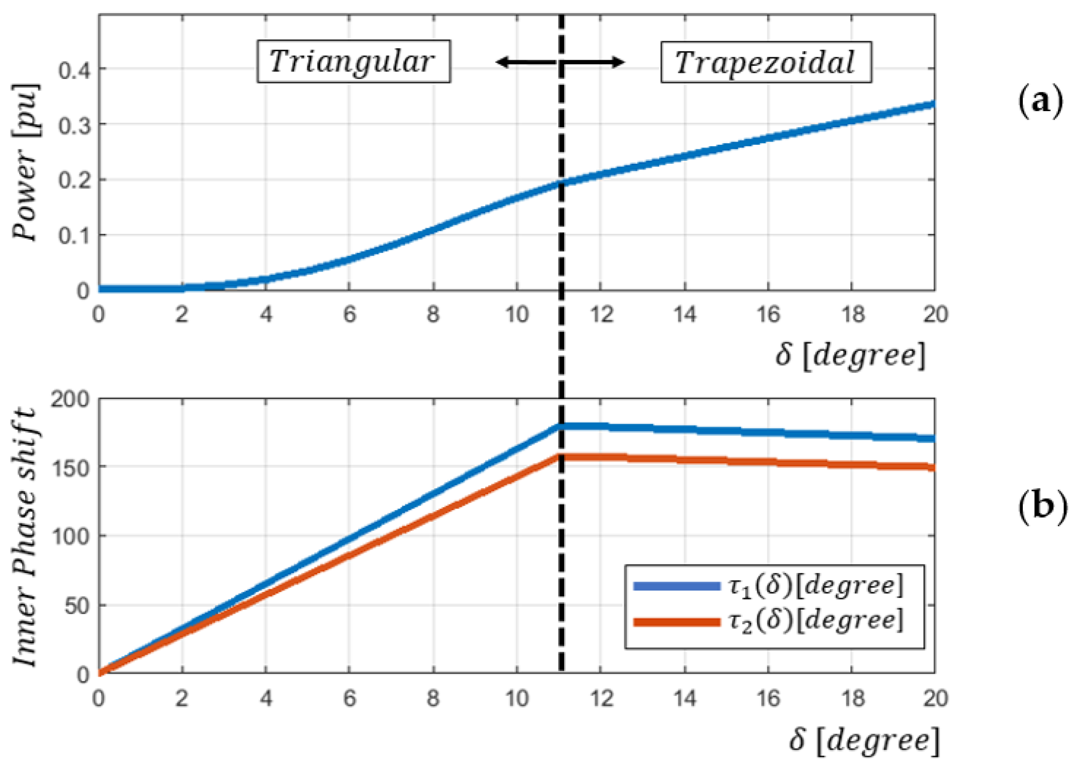
The natural transition between triangular and trapezoidal modulations is shown in
Figure 7a, where the power transferred by the converter is plotted as a function of the phase shift,
and
.
Figure 7b shows the values of
and
as a function of
.
3. Proposed Adaptive Model Predictive Control (AMPC)
In power electronics, contemporary control methods are frequently employed. MPC is one notable example.
Control methodologies that aim to reduce switching losses in the converter usually require complex algorithms to define the three control variables (, and ) to achieve the desired output voltage. In a deviation from these methods, the AMPC control uses triangular and trapezoidal modulations to reduce switching losses in the converter. The control defines the modulation to be used according to the converter operating point. The great advantage of this strategy is that there is no need for complex algorithms to define the optimal operating point. In addition, the power transfer in the converter happens smoothly and continuously during switching between triangular and trapezoidal modulations.
3.1. Mathematical Modeling
The power transferred by the converter depends on the voltages synthesized by the active bridges. In general, phase shift
and inner phase shift, represented by
and
, may be present in the pulses generated by bridges. In this case, either the phase shift or the variation in the inner phase shift may be used to regulate the power flow between the bridges. In this work, the voltages synthesized by the active bridges
and
were generated through a centralized PWM, as depicted in
Figure 2b.
The average value of ANPC-DAB output current
is obtained from phasor theory and is calculated as in (8).
where
is sample time and
is the switching frequency.
The average output capacitor quasi-instantaneous voltage is calculated as in (9).
where
and
are the measure output load current and the output capacitance of ANPC-DAB converter, respectively.
The discretization of (9), using the Euler method, defines the predicted voltage output (10).
where
and
are measured at time
and
is the defined current output derived from (8).
At instant , there will be a synthesized voltage due to the state of the switches defined by the control at instant . Between instants and , the calculation will estimate the voltages for the next cycle, i.e., at time . Therefore, this calculation must be done using the state voltage at time , when the control will decide the new state of the switches. To this end, a delay compensation is determined by calculating the voltage that will be synthesized at time so that all possible predictions for instant can be analyzed. Thus, it is necessary to calculate references for two time steps because predicting variables for only one time step is insufficient to account for the processing delay of signals.
Assuming that a sampling period’s load current does not change significantly, i.e.,
, the
possible output voltages at time
are obtained from
output current possibilities
, as shown in (11).
3.2. Definition of Phase Shift and Inner Phase Shift
In this work, the main objective of the AMPC strategy is to control the output voltage ensuring the lowest losses in the active bridges.
The first step is to define the value of the phase shift. The procedure consists of discretizing the entire operating range of the DAB converter into three phase-shift options, where one must be selected. The phase shift adopted is a compromise between the controller precision and the system transient response. These three phase-shift options are set based on the last angle taken by the control, as shown in (12).
where
is the phase shift applied at the previous instant and
is dynamically evaluated according to (13), the result of which determines whether to increase or decrease the transferred power [
21].
where
where
is the value the control will track,
is a gain, the lowest phase-shift angle is
and the greatest value for
is
.
The dynamic choice of the value ensures that when the controlled variable’s error is high, the response is accelerated by using the larger phase shift. On the other hand, small angles are used to increase precision when the error is small. The advantages of utilizing this adaptive technique include a low computational burden.
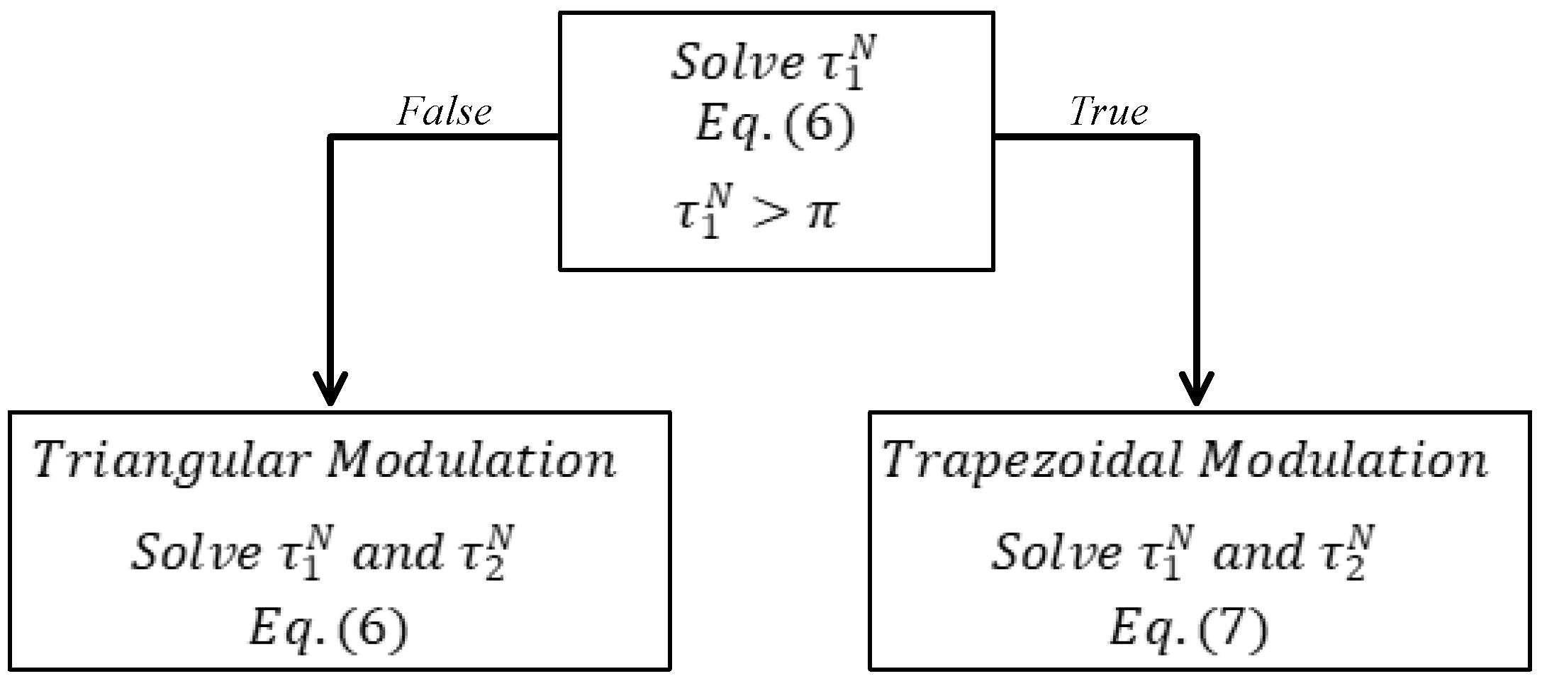
The next step is to define the modulation, i.e., the values of and . The control system will verify whether it is possible to operate with triangular modulation at the current operating point of the DAB converter, considering that this modulation promotes six soft switchings of eight commutations in one cycle. The maximum power transferred by triangular modulation occurs when the value of reaches 180°. If it is not possible to transfer the required power to the DAB converter through triangular modulation, trapezoidal modulation is used instead. Trapezoidal modulation can transfer more power than triangular modulation, but in each cycle (eight commutations), there are four soft-switching events. The values of the inner phase shift will be calculated for each value of , generating the sets and
The modulation and inner phase-shift selection algorithm are shown in
Figure 8.
3.3. Loop Compensation and Cost Function
Normally, the application of predictive control requires additional techniques to compensate for prediction errors in the controlled variables. One way to reduce these errors is to improve the mathematical model used in the control [
22,
23]. However, this solution increases the computational burden because it uses high-order models. Another method involves feedback compensation. This method has been used in several works [
24,
25,
26,
27]. In this work, the error compensation
is shown in (15). The difference between the desired and measured values of the DAB converter output voltage is added to the desired value, resulting in a compensated reference value that reduces the steady-state inaccuracy [
28].
where
is the desired voltage.
Finally, the optimal phase shift and its inner phase shift are defined by the smallest value of the cost function through the comparison between the desired value and the
values predicted by the AMPC. The cost function
is defined in (16).
where
and
are the voltage and current gains,
is the compensate reference,
is the
possibilities of output voltage value predicted,
is the
possibilities of output current value predicted, and
is the measure output current.
The first term,
, is responsible for regulating the voltage. When the output voltage is far from the target value, this term becomes dominant. As the voltage approaches the reference value, the second term,
, assumes a dominant role, preventing resonance in the output voltage. This oscillation occurs when the control variable (
,
and
) deviates from the desired operating point. The adjustment of
and
is carried out similarly to the adjustment presented in [
29] and is defined as
and
.
In addition, a penalty is imposed on the cost function if the voltage on the input capacitors drops below 80% of the nominal value. This penalty prevents the control from selecting the and phase shift presented in (12), ensuring that the converter is able to operate without drastic reduction in the voltage on the input capacitors and preventing the MOSFET’s trigger driver protection from activating due to control action.
3.4. Flow Chart of AMPC
Figure 9 shows an overview of the AMPC for output voltage, where
is the optimal phase shift and
and
are the inner phase shifts calculated as functions of
. The ANPC-DAB converter switches are triggered by the modulation control block based on the phase shift and inner phase shift delivered by the cost function. The construction of the modulation control block is described in detail in [
10].
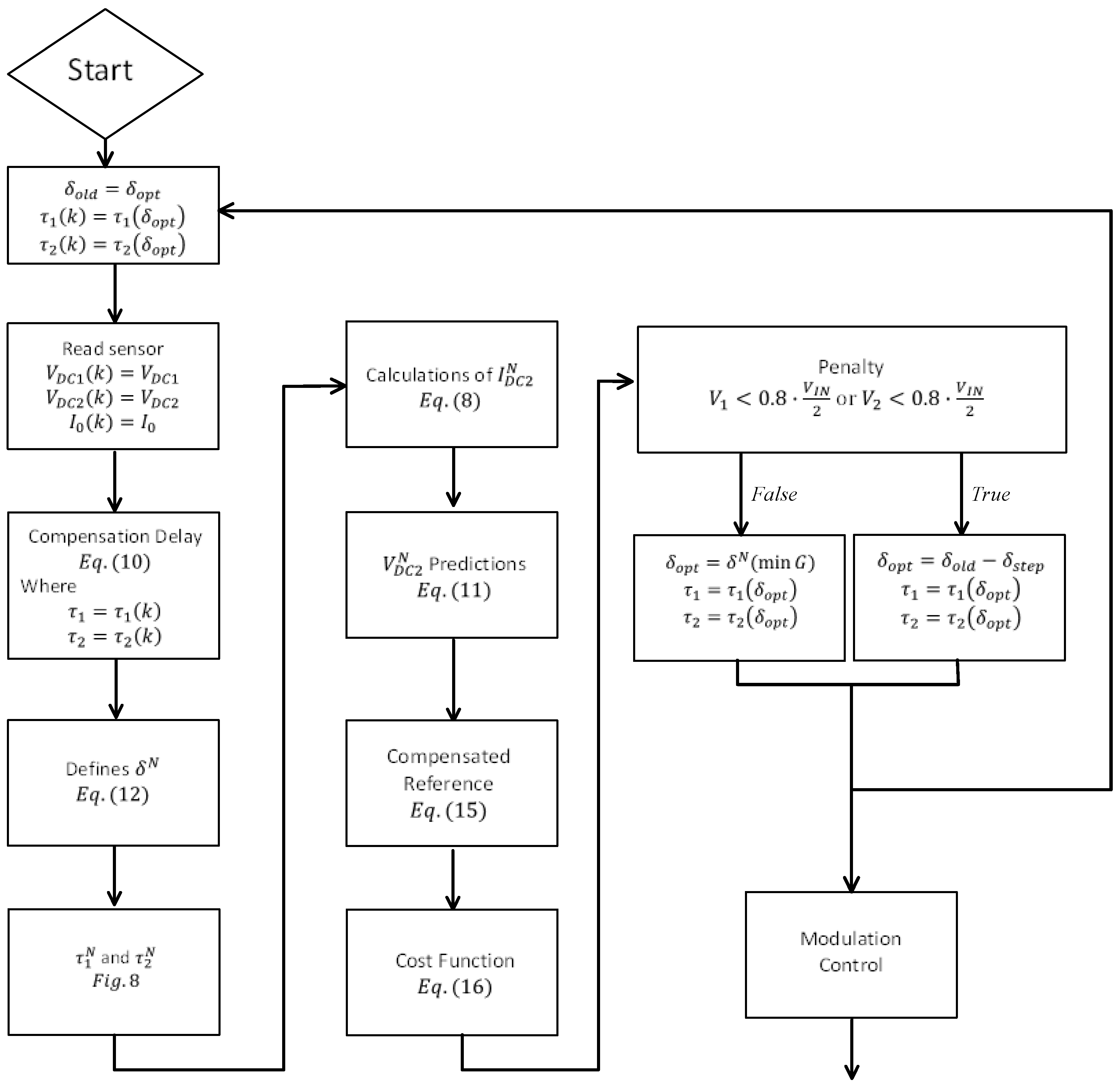
The flow chart of the proposed AMPC is presented in
Figure 10, which illustrates the calculation of AMPC from control period
to
.
The process starts by reading the sensors and saving the optimal phase shift applied at instant . The next step is to apply the compensation delay. Next, the is calculated and the three phase shifts contained in are defined. Once is defined, the values of and are calculated to define the modulation for each phase shift. The output voltage is then predicted for possibilities. The next step is to apply the reference compensation and calculate the cost function for possibilities. If the voltage on the ANPC input capacitors is below 80% of the value, the value of is adjusted to with their respective and , causing the power transmitted by the DAB to be reduced. Otherwise, is adjusted so that the cost function is minimized with their respective and .
4. Performance Analysis
This section details a performance analysis of the proposed AMPC control. Real-time simulation results using OPAL OP5700 were used to evaluate the proposed control. The specifications of the ANPC-DAB converter under evaluation are listed in
Table 2.
The ANPC-DAB converter may be affected by power-supply noise and load disturbances in real-world scenarios. Therefore, this section examines the load disturbance rejection (LDR) and source voltage disturbance rejection (SVDR), which assess the performance of the AMPC control in real-world conditions.
Another common situation in the real world involves variation in the converter parameters due to temperature. Consequently, this section evaluates the AMPC’s response to variations in the inductance and capacitance of the ANPC-DAB converter. Additionally, it examines the significance of item in the cost function.
The real-time simulation data were plotted using a graphical tool for better presentation. The original values were preserved, and no manipulations were carried out.
4.1. Source Voltage Disturbance Rejection (SVDR)
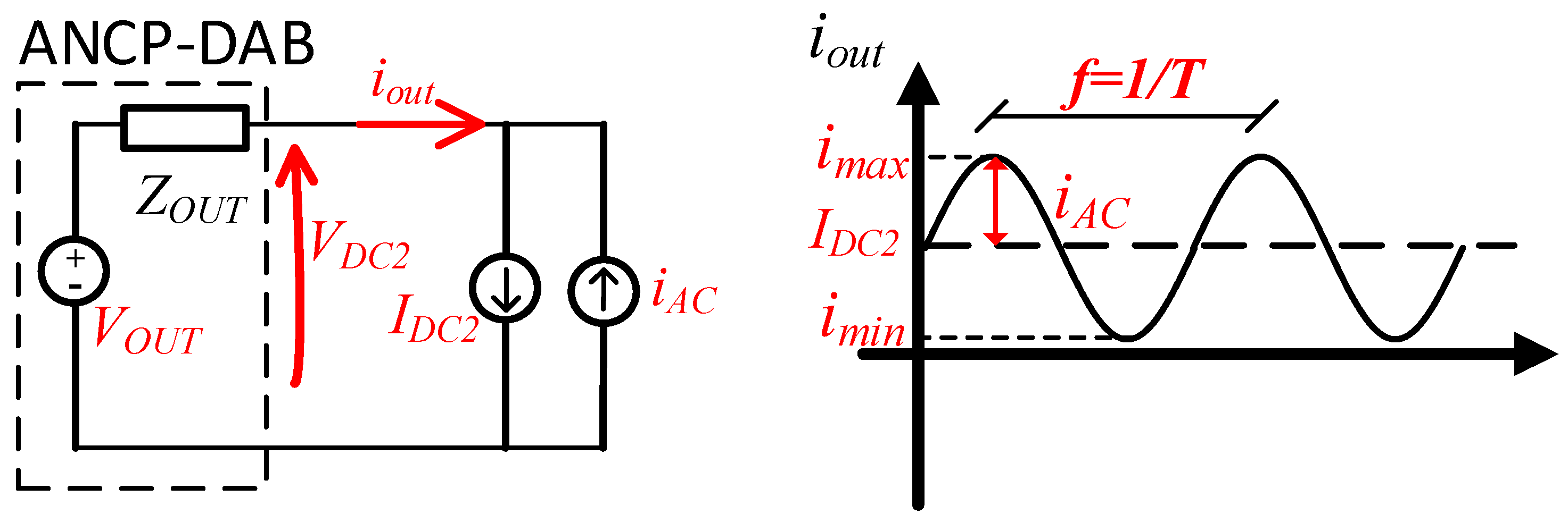
Figure 11 illustrates the circuit used in the simulation to assess the SVDR. The input voltage of the ANPC-DAB converter was decomposed into a DC component (
) and an AC component (
). The DC component represents the nominal input voltage, while
simulates source voltage disturbances. The experiment involved introducing a sinusoidal voltage with a peak value of
in series with a DC source set at
.
SVDR analysis involves Equation (18), where the output voltage
is measured for each injected frequency.
where
is the ripple value of
at frequency
and
for all analyzed frequencies.
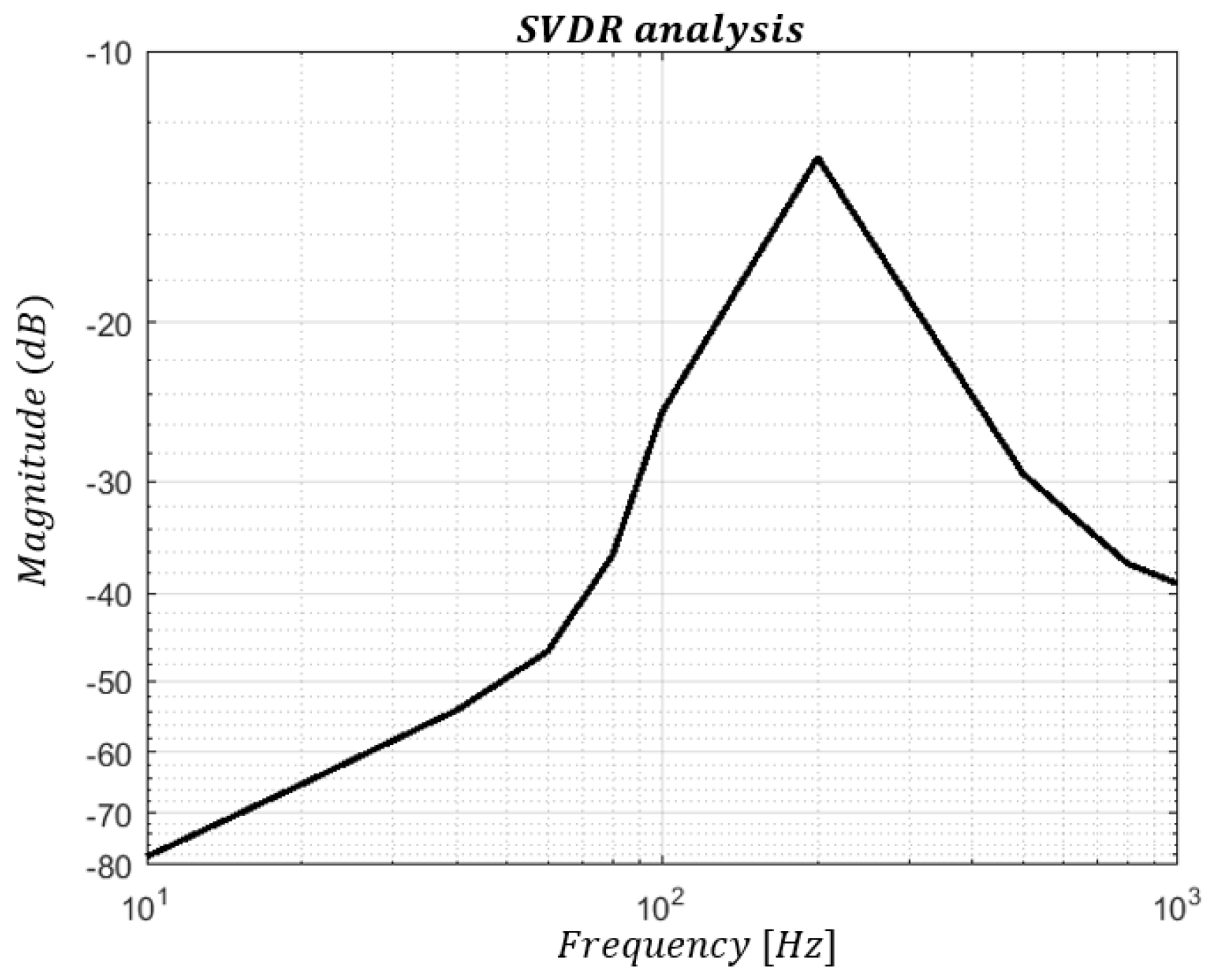
Figure 12 shows the frequency response for SVDR analysis.
The AMPC control demonstrates exceptional performance in rejecting source disturbances. In the low-frequency band, the AMPC has a lower amplitude, with a value of − at . The most significant degradation occurs at , with a higher value of −.
4.2. Load Disturbance Rejection (LDR)
When the DAB converter is applied in an SST, it can power a variety of switched loads, such as three-phase inverters, electric vehicle charging stations, and other direct current loads. Therefore, it is important to analyze the LDR of the ANPC-DAB converter. The metric used in this study was the output impedance analysis.
To illustrate this point, the converter was represented by a
source connected in series with the
output impedance, as depicted in
Figure 13.
During the analysis, the
current was set to
and the current
was added as a disturbance to simulate the load disturbance. The
value was chosen to induce a change of modulation. The output impedance was then calculated using Equation (19).
where
is the ripple value of
at frequency
f and
for all analyzed frequencies.
Figure 14 shows the frequency response for LDR analysis.
The AMPC control exhibits excellent performance in load disturbance rejection. The output impedance () increases from − to − in the frequency range of to .
4.3. Variations of Circuit Parameters
This section evaluates the robustness of the AMPC algorithm against variations in the ANPC-DAB converter parameters. The analysis is particularly significant because the converter parameters can change in real-world scenarios [
7]. For this experiment, the voltage
was varied from
to
, considering a variation of
in the values of
and
.
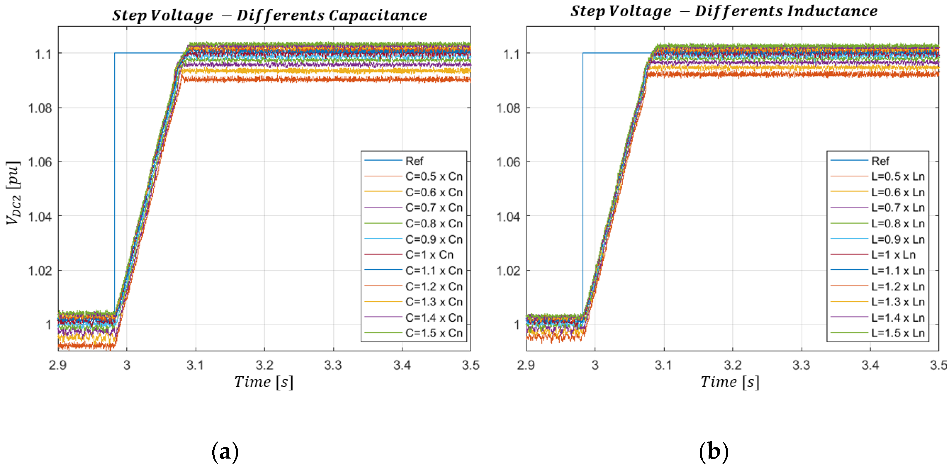
Figure 15a,b depicts the behavior of the output voltage in response to changes in capacitance
and inductance
, respectively.
Upon analysis of
Figure 15, it is apparent that variations in capacitance and inductance have minimal impacts when the circuit is in a steady state.
Table 3 presents the primary quantitative results of the ANPC-DAB converter for all the analyzed scenarios. The mean absolute error (MAE) of the
voltages for each scenario is calculated using Equation (20), where
denotes the total number of collected samples, and
and
represent the reference and measured signals, respectively, at instant
.
The results show that the control is more robust to inductor variation, yielding an MAE of . For capacitor variations, the MAE was .
4.4. Cost-Function Analysis
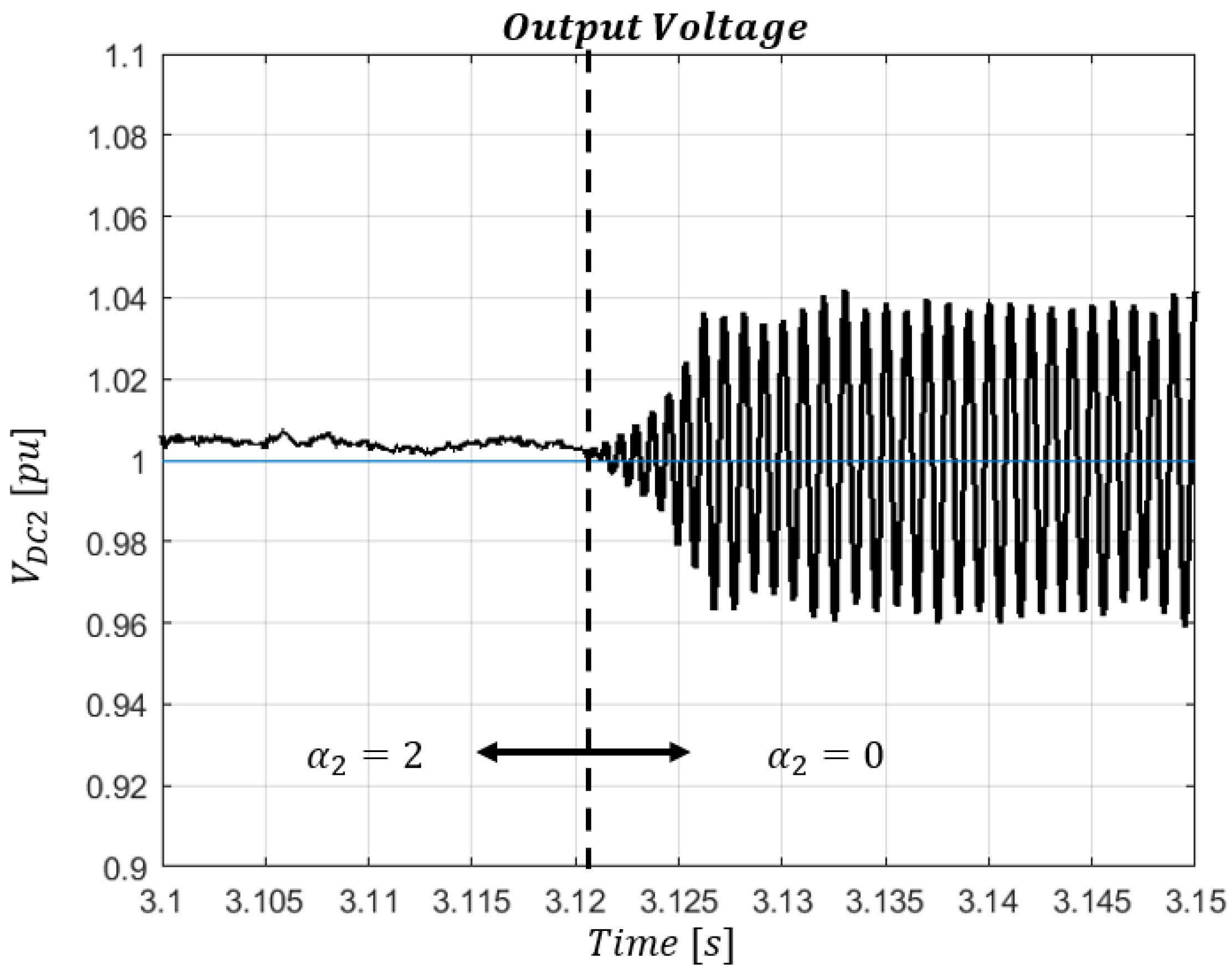
As mentioned earlier, the term in the cost function is intended to reduce the resonance at the output voltage . To demonstrate its effectiveness, the term was negated by setting during a real-time simulation, and the measured resonance frequency in this case was .
Figure 16 shows the impact of the
term on the behavior of the output voltage of the DAB converter, and it is clear that steady-state resonance is attenuated. This resonance reduction results in a decrease in acoustic noise emitted by the transformer, as well as a reduction in transformer losses.
5. Experimental Results
The AMPC control strategy was validated in a downscaled prototype in an ANPC-DAB converter operating at
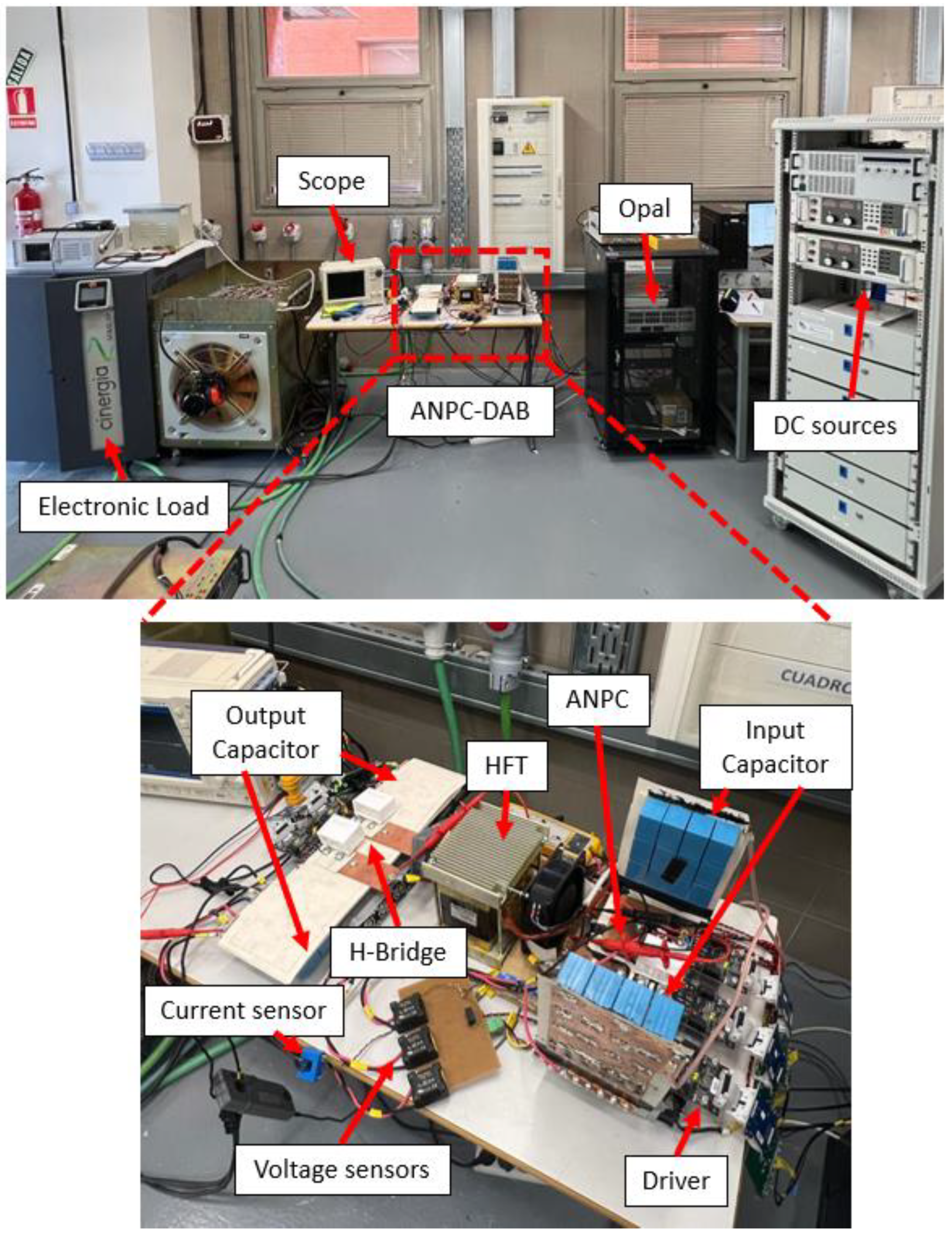
. The experimental setup is shown in
Figure 17. The platform consists of the ANPC-DAB converter, control system, load simulator and DC source.
The ANPC-DAB converter employs isolated voltage sensors, LEM DVC 1000-P (two for the ANPC input capacitors and one for the output voltage), and a current sensor, LEM LA 55-P, to monitor the output current. The ANPC and H-bridge were built using CREE CAS120M12BM2 modules, with three modules for ANPC and two modules for the H-bridge. Capacitor M119550731 77 G, , , forms one of the input capacitor banks (two blocks of 12 capacitors—) and output capacitor banks (16 capacitors—). The high-frequency transformer (HFT) has a turns ratio of and a power of .
The ANPC-DAB output load was simulated using a Cinergia GE&EL-50, a power electronics device that is capable of simulating both AC and DC electrical networks. In this study, the device was configured to simulate resistive loads. To power the converter, two ePower model SPS 15 kW programmable DC sources were used.
The control system is based on the OPAL OP5700-RCP/HIL Virtex7 FPGA-based Real-Time Simulator, which is equipped with an Intel Xeon E5 processor with 8 cores, 3.2 GHz frequency, and 20 MB cache. The test bench was developed at Laboratory of Electronic Engineering Applied to Renewable Energies, University of Alcalá de Henares, Madrid, Spain. The four analog signals from the DAB sensors are received and processed by OPAL, which generates the pulses to trigger the MOSFETs. The trigger signal is transmitted over fiber optics between OPAL and ANPC-DAB.
This study includes steady-state and transient-behavior analysis, as well as assessment of the computational burden. The steady-state performance of the ANPC-DAB converter was evaluated in terms of output voltage, AC voltages, inductor current, and global losses. Global losses were calculated by measuring the input and output power when the converter operates in steady state.
The transient behavior for using AMPC control was analyzed observing the converter output voltage. In addition, all experiments were performed with traditional MPC, referred to here as MPC, for comparisons with AMPC.
The goal was to simulate the behavior of the DC-DC stage of an SST in which one side operates at 800 V and the other at 400 V, with the ANPC-DAB converter stabilizing the voltage on the 400 V side.
5.1. Computational Burden
The computation time of the proposed AMPC was measured with OPAL resources. The AMPC controller takes to run, while the time to run MPC was . The AMPC does not use complex optimization techniques, instead requires almost the same time as the traditional MPC. When a switching frequency is utilized, is available in a single sampling period. Thus, there is enough time to implement other functionalities, such as protections, MODBUS communication etc.
5.2. Steady-State Analysis
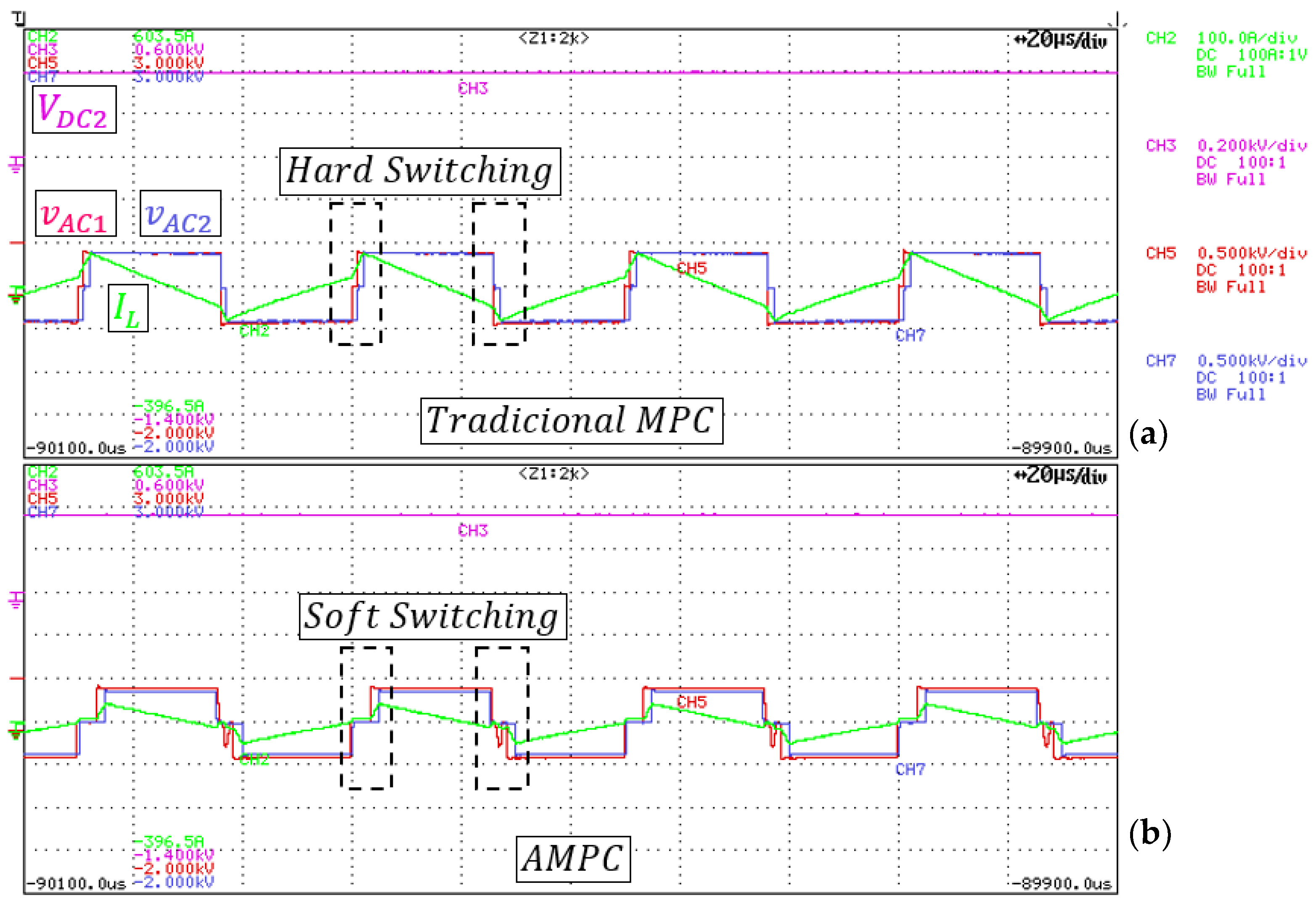
The steady-state analysis aims to compare the overall performance of the converter using AMPC to that using MPC. In the first test, the load was set to
. At this point, the AMPC operates with triangular modulation. Waveforms of
,
and
using AMPC and MPC are shown in
Figure 18a and
Figure 18b, respectively.
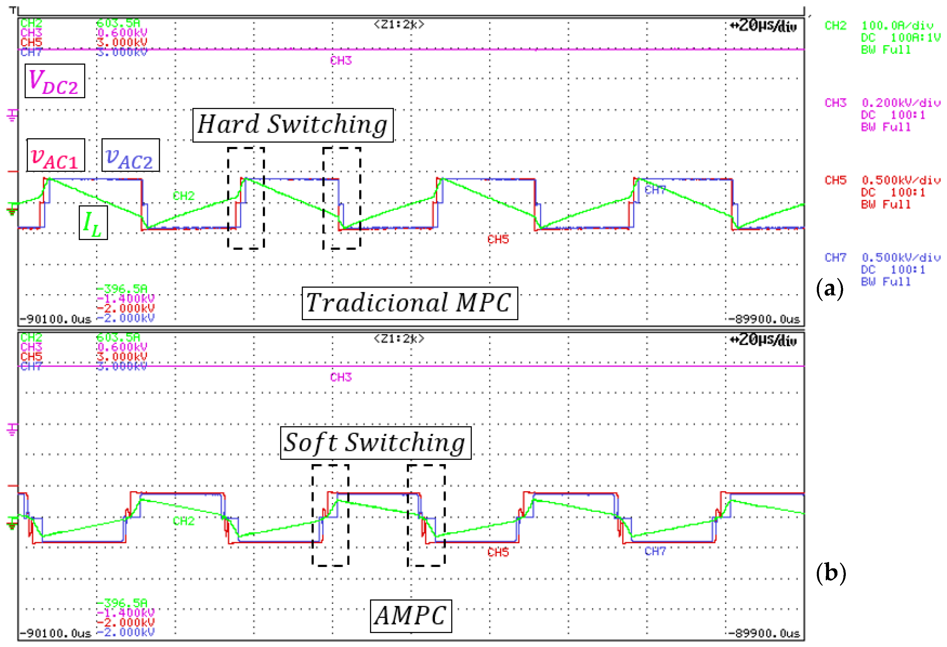
The second test load was set to
. At this point, the AMPC operates with trapezoidal modulation. Waveforms of
,
and
using MPC and AMPC are shown in
Figure 19a and
Figure 19b, respectively.
Qualitatively,
Figure 18b and
Figure 19b show that the converter operating with the MPC has hard switching in state changes (
,
, and
), whereas this change occurs in the presence of current, dissipating more power in the switches. In contrast, the AMPC control causes the converter to operate with soft switching, i.e., six soft switchings out of the eight commutations in one cycle when the control chooses triangular modulation and four soft switchings out of the eight commutations in one cycle when the control chooses trapezoidal modulation.
Table 4 presents values of input voltage, output voltage, input current, and output current for the two operating points mentioned above with MPC and AMPC control.
The proposed AMPC control demonstrated accurate response, with less than error on the output voltage mean value. This control increased the converter’s global efficiency without changing the hardware or increasing computational efforts. In microgrid applications, where the SST operates at low loads for extended periods, high efficiency is essential. The AMPC control strategy can save approximately of energy in one year of operation (, 18 h of low load per day), equivalent to the monthly consumption of three houses with a usage, simply through use of the AMPC control.
5.3. Transient Analysis
The transient behavior of the AMPC control was analyzed for load and voltage step on the converter. The MPC control was subjected to the same analyses for comparison purposes.
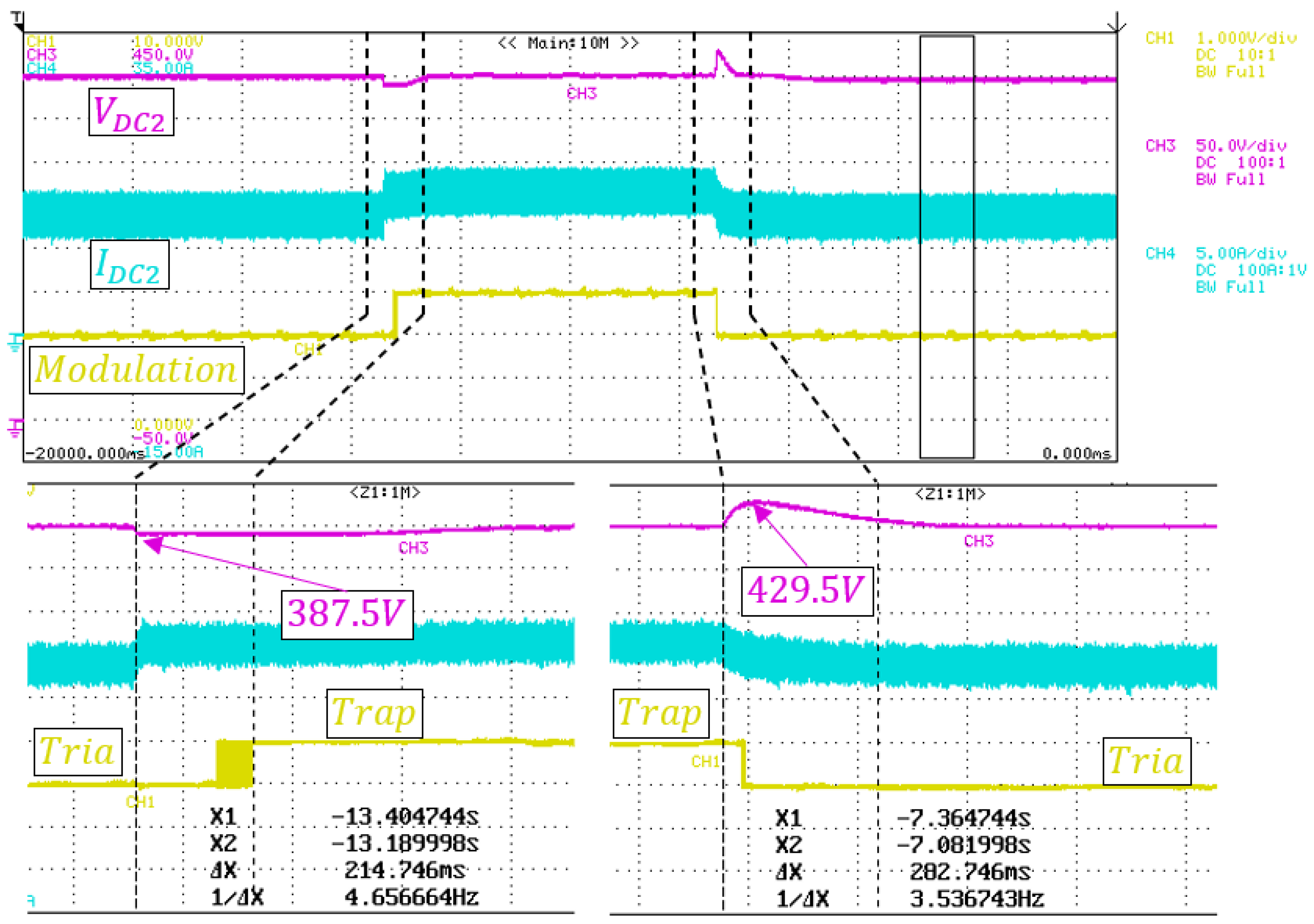
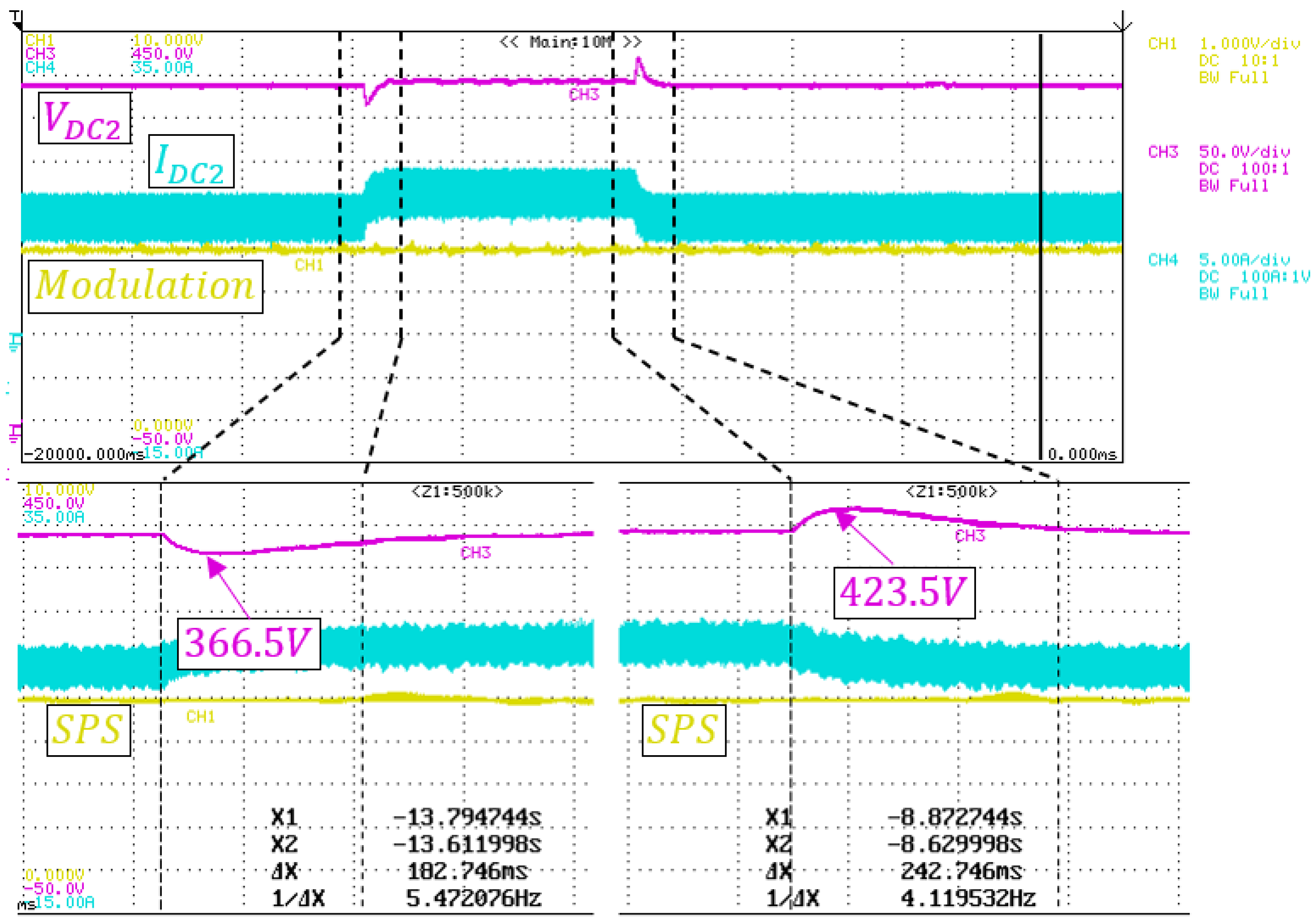
In the first experiment, the load was changed from to to evaluate the response of the AMPC to a modulation change, which is a critical situation. In order to visualize the chosen modulation on the scope within other DAB variables, an analog output was used, where indicates triangular modulation, indicates trapezoidal modulation, and indicates SPS modulation (used in MPC).
Figure 20 and
Figure 21 show the behavior of the output voltage for AMPC and the MPC controls, respectively, where the purple, blue, and yellow lines are the
voltage, the
current, and the modulation used by the control, respectively.
The AMPC control can keep the output voltage stable and choose between triangular and trapezoidal modulations according to the operating point, ensuring better converter efficiency. The response time was less than
with an overshoot of less than
. Comparing traditional MPC with AMPC, the differences in transient behavior are small. The summarized results of the experiment are shown in
Table 5.
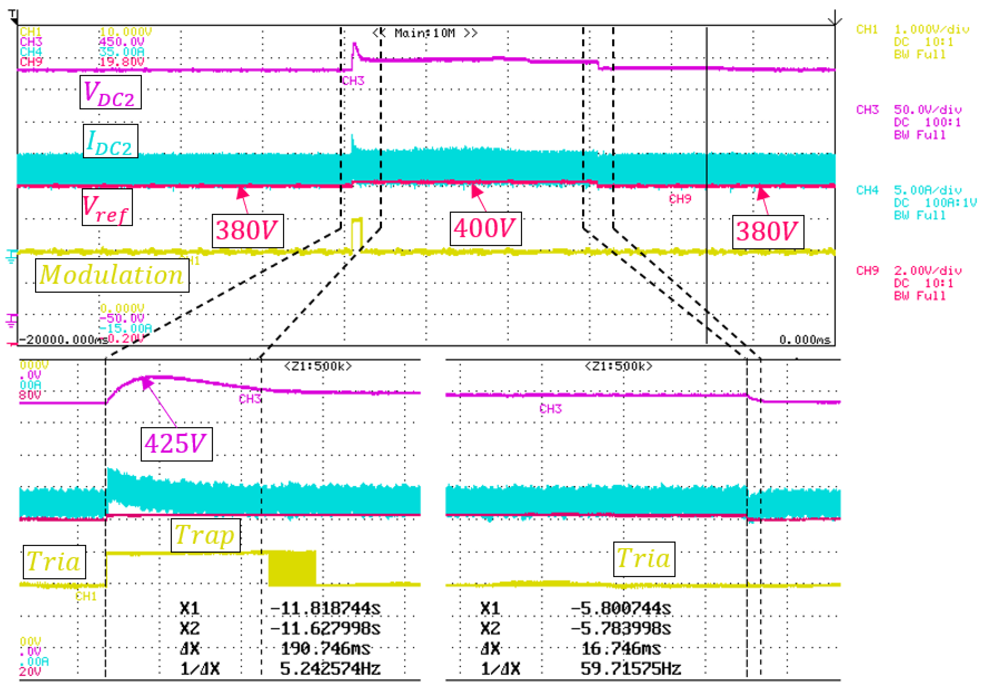
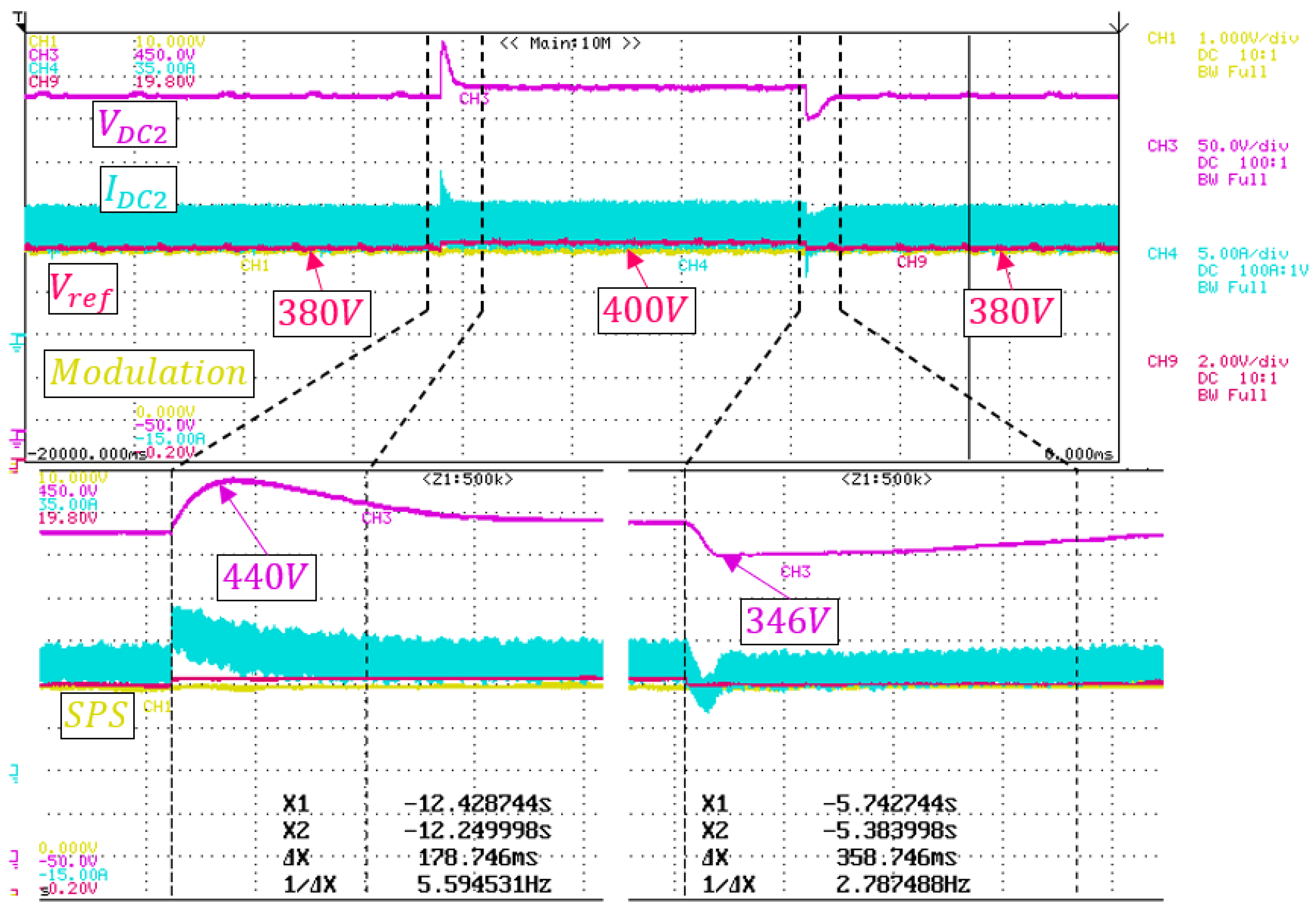
In the second experiment, the
voltage was changed from
to
.
Figure 22 and
Figure 23 show the behavior of the AMPC and the MPC controls, respectively, where the purple, blue, yellow, and red lines are the
voltage, the
current, the modulation used by the control, and the desired value for the output voltage
, respectively.
In this scenario, the AMPC strategy dynamically changes the phase shift and inner phase shift in order to charge the output capacitor so that the voltage reach the new requested reference value.
AMPC and MPC showed similar performance. However, in the transition
there was no undervoltage and the settling time was much shorter than in the MPC. The summarized results of the experiment are shown in
Table 6.
Unlike a simulated environment, the converter’s transient power transfer is limited, which delays the response time in relation to other topologies. The insertion of the penalty in the cost function prevents the ANPC input capacitor from discharging to levels that cause the MOSFET’s protection trigger drivers to activate.
6. Discussion
The DAB converter has many advantages for use in SSTs, including galvanic isolation, bidirectional power flow, high power density, and the ability to operate as a buck or boost with ZVS over a wide range. However, low loads and high voltages can pose challenges to its efficiency and operation capacity. To address this difficulty, multilevel topologies such as the ANPC-DAB can be used. In this topology, ANPC is applied on the high-voltage side and an H-bridge is used on the low-voltage side. Experiments were conducted on an prototype.
The traditional control method used in the DAB converter controls only the phase shift, limiting its efficiency at low loads. To improve efficiency at low loads, different modulations can be used to enable soft switching throughout the operating range. However, these solutions require the selection of voltage values for the converter’s active bridges, which involves complex optimization methods that can increase computational costs and hinder practical application.
MPC is an advanced technique used in many electrical systems. Unlike conventional control, it predicts the system’s future behavior using mathematical modeling and calculates an optimal control signal to maintain the desired output. To enhance efficiency at low loads, AMPC control, which employs triangular and trapezoidal modulations, is used. The natural transition between these modulations results in a gradual change in the inductor’s current waveform from triangular to trapezoidal or vice versa. This method is used to obtain the highest efficiency when the DAB converter operates at low loads.
Real-time simulation was used to evaluate the frequency response and robustness of the AMPC applied to the ANPC-DAB topology. The converter attenuates voltage-source noise by − at low frequencies, with the worst case at , at which it attenuates the disturbance by −. Additionally, AMPC offers low output impedance, allowing for high-intensity output current without significant voltage drops, which is essential for maintaining output current stability in applications with load variations.
Robustness tests were conducted by varying the power transfer inductance and output capacitance. There are several approaches to designing predictive controllers that are robust to converter parameter variations. In this work, the reference is adjusted to ensure lower error when the converter operates in steady state. Mean absolute error (MAE) values of and were obtained for a variation in the nominal values for the inductor and capacitor, respectively.
The impact of the term in the cost function on the output voltage was demonstrated. When , a resonance occurs in the output voltage, even in steady state. Resonance can cause system instability, low performance, electrical noise, and electromagnetic interference, which can affect nearby electronic systems. Therefore, the importance of the term in reducing oscillations in the system is evident.
Experimental results from the prototype indicate a significant improvement in converter efficiency with the AMPC control, achieving at and at in steady state, compared to and , respectively, with the MPC. While the dynamic response of the AMPC control did not differ significantly from that of the MPC, the MPC was faster and the AMPC showed smaller overshoots in most of the tests.
Finally, an important advantage of AMPC is that it eliminates the need for complex optimization processes to choose the phase shift and inner phase shift, while also avoiding the need for intense computational efforts. This study shows that the processing time difference between MPC and AMPC is only .
For future work, the control methodology discussed in this study can be applied to input series output parallel (ISOP) structures to verify the energy efficiency of the structure and evaluate the control behavior for transient situations and steady-state operation.
7. Conclusions
The present article proposes the application of the advanced AMPC control technique in the ANPC-DAB topology. This topology enables the converter to operate at high voltages, providing an alternative to ISOP structures, which operate in series and parallel.
Several real-time simulated analyses have shown that the AMPC control has high capacity for voltage-source noise rejection and exhibits low output impedance. Additionally, dynamic reference adjustment has improved the control’s robustness to variations in converter parameters.
The experimental results from the prototype showed excellent dynamic and steady-state performance. The AMPC exhibited dynamic response similar to that of the MPC. However, in steady state, the efficiency of the converter was significantly improved with use of the AMPC, reaching at and at in steady state, compared to and , respectively, without the AMPC. Additionally, the control achieved error rates below in relation to the desired value.
Despite the benefits of using AMPC, the computational cost was not significantly increased compared to MPC. The processing time was measured using OPAL resources, which showed that the MPC processing time was , while that of the AMPC was . Considering that the processor has available (), applying AMPC leaves enough time for other applications, such as protections and data communication.

