Article

Analysis and Design of a New High Voltage Gain Interleaved DC–DC Converter with Three-Winding Coupled Inductors for Renewable Energy Systems

1
Department of Electrical Engineering, Kun Shan University, Tainan 710303, Taiwan
2
Green Energy Technology Research Center, Kun Shan University, Tainan 710303, Taiwan
*
Author to whom correspondence should be addressed.
Energies 2023, 16(9), 3958; https://doi.org/10.3390/en16093958
Submission received: 1 March 2023 / Revised: 28 April 2023 / Accepted: 5 May 2023 / Published: 8 May 2023
(This article belongs to the Special Issue Advanced Application of Power Electronics in Power Systems)

Abstract

:
In this article, a new non-isolated interleaved DC–DC converter is proposed to provide a high voltage conversion ratio in renewable energy systems. The converter configuration is composed of a two-phase interleaved boost converter integrating a voltage-lift capacitor and three-winding coupled inductor-based voltage multiplier modules to achieve high step-up voltage conversion and reduce voltage stresses on the semiconductors (switches and diodes). The converter can achieve a high voltage conversion ratio when working at a proper duty ratio. The voltage stresses on the switches are significantly lower than the output voltage, which enables engineers to adopt low-voltage-rating MOSFETs with low on-state resistance. The switches can turn on under zero-current switching (ZCS) conditions because of the leakage inductor series reducing switching losses. Some diodes can naturally turn off under ZCS conditions to alleviate the reverse–recovery issue and to reduce reverse–recovery losses. The input current has small ripples due to the interleaved operation. The leakage inductor energy is recycled and voltage spikes on the switches are avoided. The proposed converter is suitable for applications in which high voltage gain, high efficiency and high power are required. The principle of operation, steady-state analysis and design considerations of the proposed converter are described in detail. In addition, a closed-loop controller is designed to reduce the effect of input voltage fluctuation and load change on the output voltage. Finally, a 1000 W laboratory prototype is built and tested. The theoretical analysis and the performance of the proposed converter were validated by the experimental results.

1. Introduction

The demand for renewable energies, such as fuel cells and photovoltaic arrays, has dramatically increased for electricity generation because of the shortage of fossil fuels and the growing climate change impacts [1]. The renewable energy system is shown in Figure 1. A 380 or 400 Vdc dc-bus voltage is necessary for grid-connected applications if the line voltage of the utility grid is 220 Vac. However, the output voltages of fuel cells and photovoltaic arrays are typically lower than 50 V. Therefore, DC–DC converters with high voltage conversion ratios are necessary to boost the low voltages of green energy resources to the high dc-bus voltage required in renewable energy system applications.
High voltage gain DC–DC converters can be mainly divided into two types: isolated and non-isolated. The traditional isolated type adjusts the transformer turns ratio to obtain high voltage gain, such as in push–pull, half-bridge, forward and flyback DC–DC converters. However, high leakage inductance derived from the high turns ratio may result in high voltage spikes and poor efficiency. A boost converter of the non-isolated type can, theoretically, achieve high voltage gain by operating at a very large duty ratio. However, the voltage conversion ratio is practically limited due to parasitic elements [2]. In general, high voltage rated MOSFETs have the characteristic of high on-state resistance RDS(ON), and the high voltage-rated diodes have high forward voltage drop. Therefore, a high voltage gain DC–DC converter, having low voltage stresses on the switches and diodes, can contribute to reducing conduction losses. Consequently, low semiconductor voltage stress is important for efficiency considerations in the new high voltage gain converter topology.
In recent years, high voltage gain DC–DC converters have been researched in depth by means of different voltage-boosting techniques. The most widely used method is based on the coupled inductor technique. In [3], a coupled inductor-based soft switched high step-up converter with a voltage multiplier cell was proposed for DC microgrid applications. In [4], five categories of high step-up coupled-inductor boost converters were reviewed. Two configurations for two- and three-winding coupled inductor-based high step-up DC–DC converters were proposed for sustainable energy applications in [5]. In [6], a three-winding coupled inductor-based high voltage gain DC–DC converter was proposed for photovoltaic (PV) systems. The turns ratio of the coupled inductor can be utilized to increase design freedom for the voltage conversion ratio in addition to the duty ratio. The winding cross-coupled inductor contributes to the current sharing performance of the interleaved two-phase converter [7]. The voltage multiplier cell (VMC) is often composed of a coupled inductor and diode–capacitor to further extend the voltage gain and reduce the switch voltage stress [8,9,10,11]. A converter topology that integrates a built-in transformer, coupled inductor, diode and capacitor is proposed to extend the higher voltage gain [12,13]. To achieve high voltage gain with simple circuit structures a number of approaches have been proposed, such as the following: transformer-less and coupled inductor-less techniques of a hybrid switched-inductor in [14], modified active switched-inductor in [15], active switched-inductor and passive switched-capacitors in [16,17] and switched-capacitor in [18]. Three-level DC–DC converters have a simple configuration and decrease the switch voltage stress to half the output voltage [19,20]. To reduce switching losses, zero-voltage switching (ZVS) or zero-current switching (ZCS) in high voltage gain DC–DC converters were proposed in [21,22,23]. The review papers provide good references for research on high voltage gain DC–DC converters [24,25,26,27].
A new non-isolated high voltage gain, interleaved DC–DC converter, suitable for renewable energy applications, is proposed in this article. The techniques of voltage-lift, three-winding coupled inductors and voltage multiplier modules are used to increase the voltage conversion ratio and to reduce the voltage stresses on the power devices.
The characteristics and benefits of the presented converter are summarized as follows:
(1)
The high voltage gain of the proposed converter can be obtained with an appropriate duty ratio.
(2)
Low voltage-rated MOSFETs with low on-state resistance RDS(ON) and low voltage-rated diodes with low forward voltage drop can be adopted to reduce conduction losses, due to their having low voltage stresses.
(3)
The switches turn ON under the ZCS condition to reduce switching losses.
(4)
The diode reverse–recovery issue is mitigated due to the leakage inductors of the coupled inductors, and voltage spikes on the switches are avoided because the leakage energy is recycled.
(5)
The interleaved parallel input structure of the presented configuration decreases current stresses on the power devices and reduces the input current ripple.
The rest of this article is organized as follows. The operational principle of the proposed converter is presented in detail in Section 2. The steady-state analysis is given in Section 3. The driving circuit and the closed-loop controller design is demonstrated in Section 4. Section 5 demonstrates the simulation and experimental results when using a 1000 W laboratory prototype to validate the theoretical analysis and to assess the effectiveness of the presented converter. This article is concluded in Section 6.

2. Proposed Converter and Principle of Operation

2.1. Proposed Converter

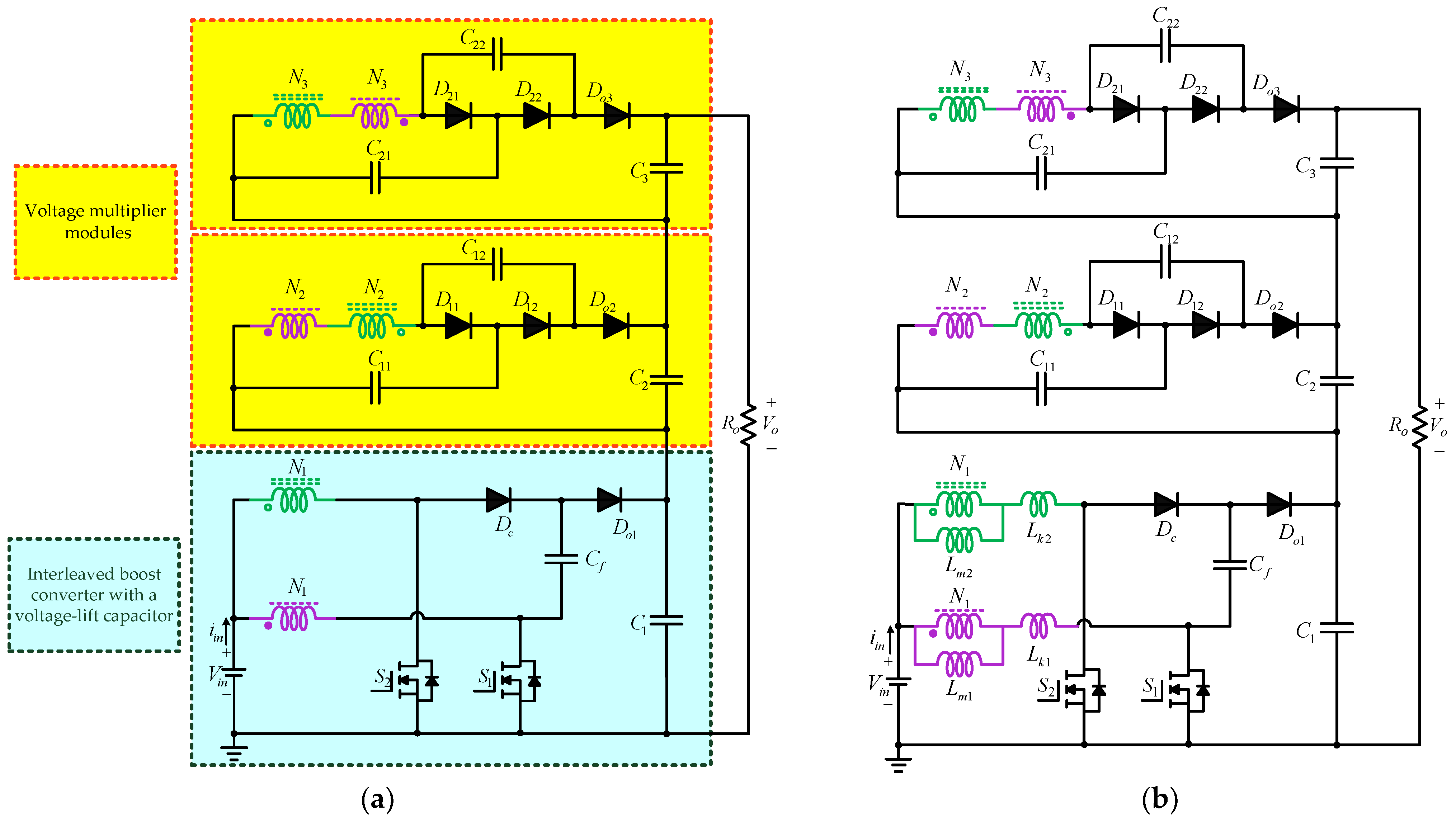
The circuit configuration of the proposed converter topology is shown in Figure 2a. The proposed converter has two coupled inductors with three windings. Their own coupling references are denoted “ “ and “ “.
The first winding of each coupled inductor acts as an input filter inductor. The second and third windings of the coupled inductors are inserted in series integrating capacitors and diodes to form two voltage multiplier modules (VMMs). It should be pointed out that the arrangement positions of the series windings are different in the two VMMs, so that the output capacitors, C 2 and C 3 , can be charged and discharged alternately to reduce the output voltage ripple. The proposed converter primarily consists of two parts: one part is the interleaved boost converter integrating a voltage-lift capacitor, and the other part is the stacked structure of two voltage multiplier modules on the output side to further extend the voltage gain and reduce the voltage stresses on the power devices. Interleaved operation is adopted to help the current ripple cancellation on the input side.
Figure 2a, S 1 and S 2 present the following power switches: C f is the voltage-lift capacitor, C 1 , C 2 and C 3 are the output capacitors, C 11 and C 21 are the regenerative capacitors, C 12 and C 22 are the voltage-doubler capacitors, D c is the clamp diode, D o 1 , D o 2 and D o 3 are the output diodes, D 11 and D 21 are the regenerative diodes, D 12 and D 22 are the voltage-doubler diodes and R o is the output load. The equivalent circuits for the coupled inductors consist of the ideal transformers with a turns ratio N 1 : N 2 : N 3 , the magnetizing inductors L m 1 and L m 2 , and the leakage inductors L k 1 and L k 2 . Figure 2b shows the equivalent circuit of the presented converter.

2.2. Operational Principle

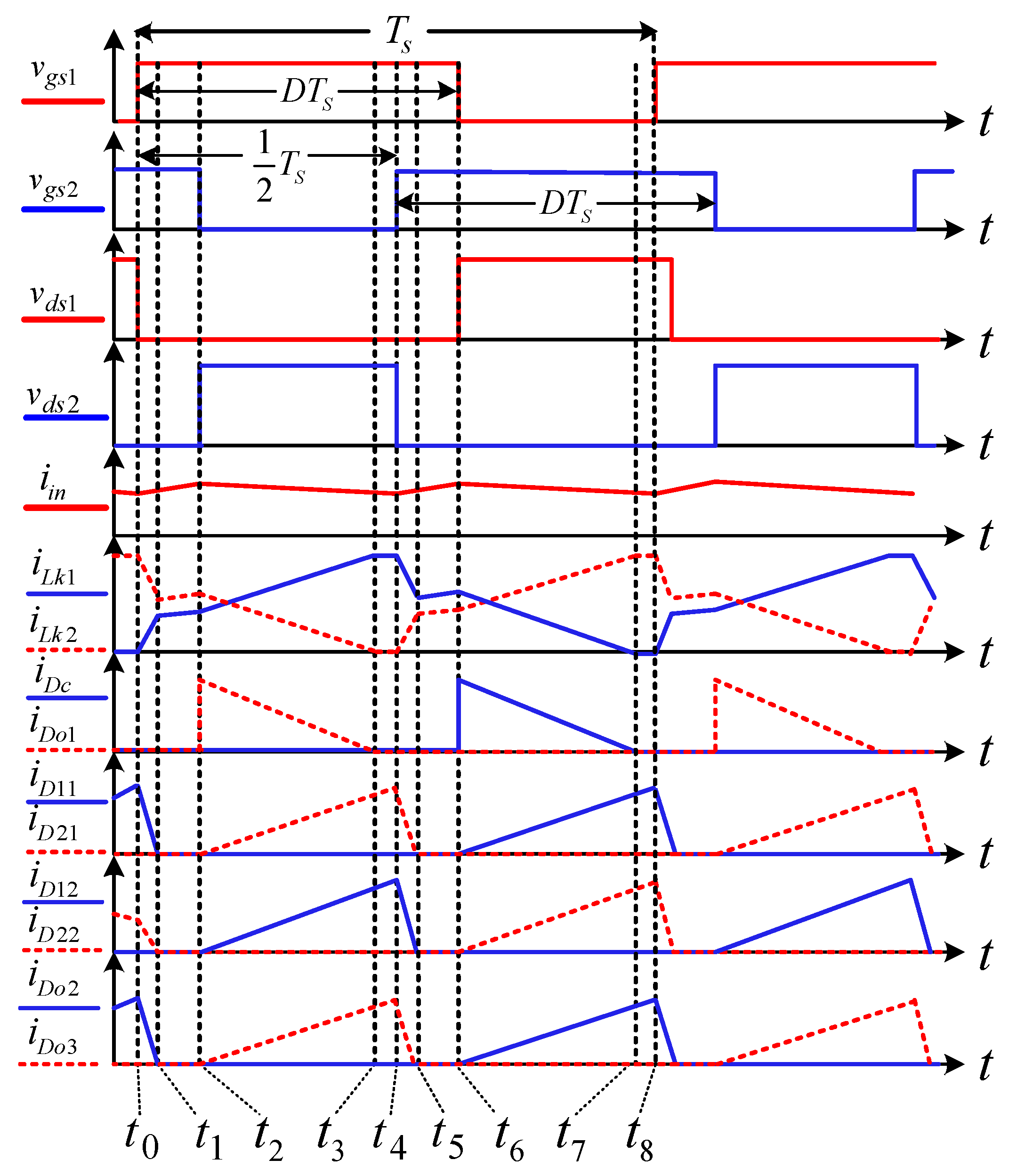
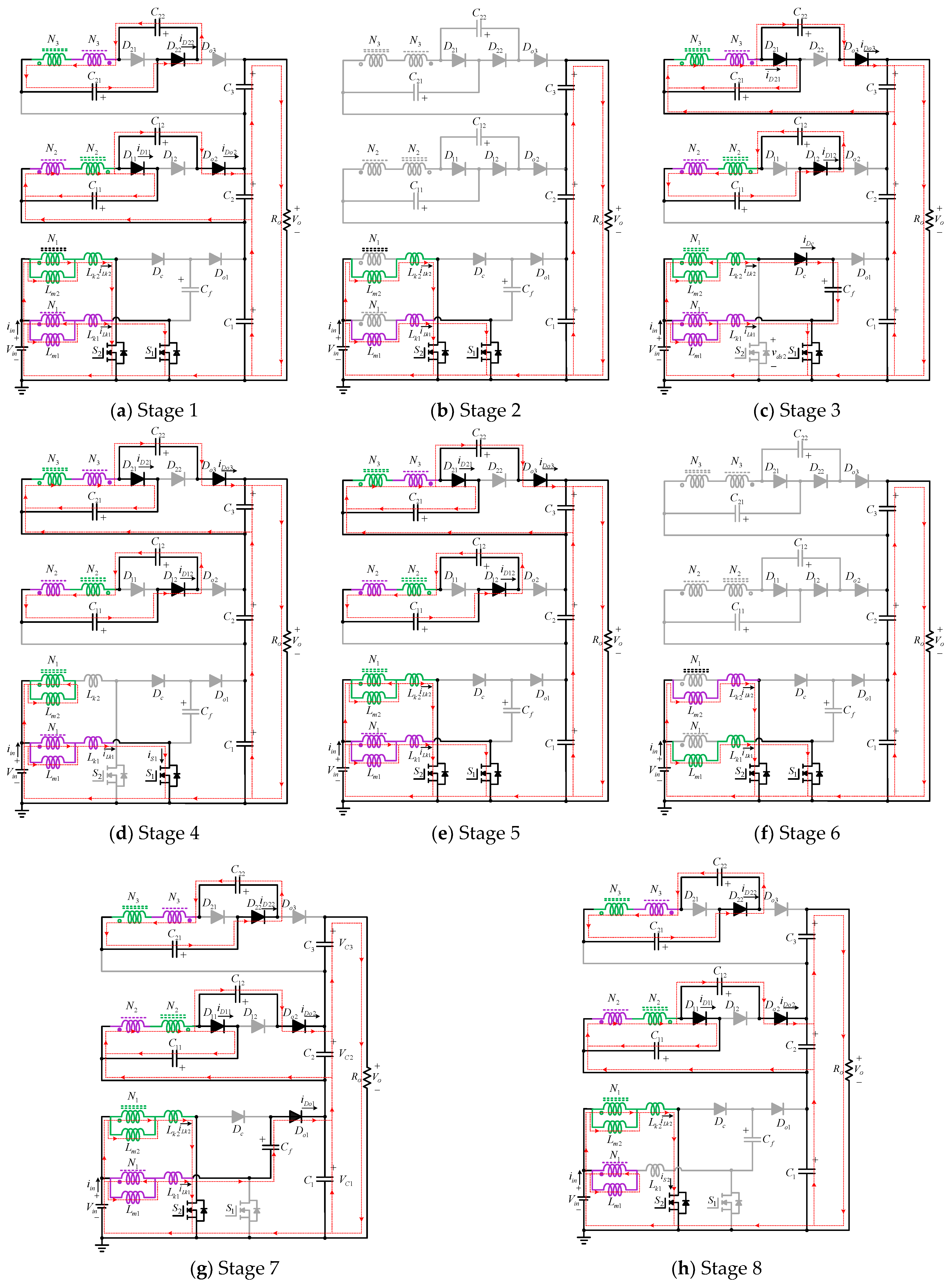
The switches S 1 and S 2 operate in an interleaved manner with phase shift 180 ° to lower the input current ripple due to ripple cancellation. The duty ratio of the switches is greater than 0.5 for high step-up voltage gain purposes. The key steady-state waveforms of the presented converter, operating in continuous conduction mode (CCM), are shown in Figure 3. According to the ON/OFF state of the switches and diodes in one switching period, the converter has eight operational stages, as illustrated in Figure 4.
In order to simplify the circuit analysis, some assumptions are made, as follow:
  • All semiconductors (switches and diodes) are considered to be ideal.
  • All capacitors are sufficiently large, and the voltages on these capacitors are regarded as constant during one switching period.
  • The parameters of the three-winding coupled inductors are regarded as being identical; that is, the turns ratio n = N 2 / N 1 = N 3 / N 1 , L m 1 = L m 2 = L m and L k 1 = L k 2 = L k . The coupling coefficient of the coupled inductor is defined as k = L m / ( L m + L k ) .
Stage 1 [ t 0 ~ t 1 ]: At the beginning of this stage, switch S 1 starts to conduct and S 2 keeps to the on-state. The diodes D o 1 , D c , D 12 , D 21 and D o 3 are reverse-biased. Due to the existence of leakage inductor L k 1 and the initial current i L k 1 ( t 0 ) = 0 , S 1 achieves ZCS turn-on because of the leakage inductor series. In this stage, the leakage current i L k 1 increases rapidly from its initial value (zero). The magnetizing energy stored in L m 1 still transfers to the second and third windings of the coupled inductor when i L k 1 < i L m 1 . The currents i D 11 , i D 22 and i D o 2 decrease and the descent rate is limited by the leakage inductors L k 1 and L k 2 . Therefore, the reverse-recovery issue of these diodes is lessened.
When the leakage current i L k 1 rises to reach i L k 1 = i L m 1 at t = t 1 , the currents i D 11 , i D o 2 and i D 22 decrease to zero. The diodes D 11 , D o 2 and D 22 turn OFF under the ZCS condition. During this stage, the leakage current i L k 1 is given by
i L k 1 ( t ) = i L m 1 ( t ) n i D 11 ( t ) + i D o 2 ( t ) + i D 22 ( t )
Stage 2 [ t 1 ~ t 2 ]: The switches S 1 and S 2 are turned ON, and all diodes are reverse-biased during this stage. The input voltage V i n supplies energy to the magnetizing inductors L m 1 and L m 2 as well as the leakage inductors L k 1 and L k 2 . The leakage currents i L k 1 and i L k 2 increase linearly. The output capacitors C 1 , C 2 and C 3 provide energy to the output load. When the switch S 2 is turned OFF, the stage ends. During this stage, the leakage currents can be represented as
i L k 1 t = i L k 1 t 1 + V i n L m 1 + L k 1 t t 1
i L k 2 t = i L k 2 t 1 + V i n L m 2 + L k 2 t t 1
Stage 3 [ t 2 ~ t 3 ]: The switch S 2 is turned OFF at t = t 2 . The clamp diode D c begins to conduct because the leakage current i L k 2 is continuous. The diodes D 12 , D 21 , D o 3 and D c are forward-biased. The current i L k 2 flows through D c , C f and S 1 to charge the voltage-lift capacitor C f . The voltage across S 2 is clamped by the capacitor voltage V C f . The leakage current i L k 2 decreases and the energy stored in the magnetizing inductor L m 2 is transferred to charge the capacitors C 12 and C 21 via the second and third windings of the coupled inductor during this stage. In the meantime, capacitors C 11 and C 22 are discharged. This stage is terminated when i L k 2 falls to zero at t = t 3 .
Stage 4 [ t 3 ~ t 4 ]: At the beginning of this stage, the leakage energy stored in L k 2 is released completely. The clamp diode D c is turned OFF with ZCS naturally. The magnetizing current i L m 2 is reflected from the first winding to the second and third windings completely. The operation of this stage is similar to stage 3. This stage ends when switch S 2 returns to conduct at t = t 4 . The switch current i S 1 is equal to the sum of i L m 1 and i L m 2 during this stage, which can be written as
i S 1 ( t ) = i L m 1 ( t ) + n i D 12 ( t ) + i D 21 ( t ) + i D o 3 ( t ) = i L m 1 ( t ) + i L m 2 ( t )
Stage 5 [ t 4 ~ t 5 ]: At the beginning of this stage, switch S 2 starts to conduct and S 1 keeps to the on-state. The diodes D o 1 , D c , D 11 , D o 2 and D 22 are reverse-biased. Due to the existence of leakage inductor L k 2 and the initial current i L k 2 ( t 4 ) = 0 , S 2 achieves ZCS turn-on because of the leakage inductor series. In this stage, the leakage current i L k 2 increases rapidly from its initial value (zero). The magnetizing energy stored in L m 2 still transfers to the second and third windings of the coupled inductor when i L k 2 < i L m 2 . The currents i D 12 , i D 21 and i D o 3 decrease and the descent rate is limited by the leakage inductors L k 1 and L k 2 . Therefore, the reverse-recovery issue of these diodes is lessened.
When the leakage current i L k 2 rises to reach i L k 2 = i L m 2 at t = t 5 , the currents i D 12 , i D 21 and i D o 3 decrease to zero. The diodes D 12 , D 21 and D o 3 are turned OFF with the ZCS condition. During this stage, the leakage current i L k 2 is given by
i L k 2 ( t ) = i L m 2 ( t ) n ( i D 21 ( t ) + i D 12 ( t ) ) + i D o 3 ( t )
Stage 6 [ t 5 ~ t 6 ]: The switches S 1 and S 2 conduct, and all diodes are reverse-biased during this stage. The magnetizing inductors L m 1 and L m 2 as well as the leakage inductors L k 1 and L k 2 are supplied with energy by the input voltage V i n . The leakage currents i L k 1 and i L k 2 increase linearly. The output capacitors C 1 , C 2 and C 3 provide energy to the output load. The stage ends when switch S 1 is turned OFF. During this stage, the leakage currents can be represented as
i L k 1 t = i L k 1 t 5 + V i n L m 1 + L k 1 t t 5
i L k 2 t = i L k 2 t 5 + V i n L m 2 + L k 2 t t 5
Stage 7 [ t 6 ~ t 7 ]: Switch S 1 is turned OFF at t = t 6 . The output diode D o 1 begins to conduct because the leakage current i L k 1 is continuous. The diodes D 11 , D 22 , D o 1 and D o 2 are forward-biased. The leakage current i L k 1 flows through D o 1 , C f and C 1 to charge the output capacitor C 1 and to discharge the voltage-lift capacitor C f . The voltage across S 2 is clamped by the voltages on the capacitors C f and C 1 . The switch voltage stress is equal to V C f + V C 1 . During this stage, the leakage current i L k 1 decreases and the energy stored in the magnetizing inductor L m 1 is transferred to charge the capacitors C 11 and C 22 via the second third windings of the coupled inductor. In the meantime, capacitors C 12 and C 21 are discharged. This stage is terminated when the leakage current i L k 1 decreases to zero at t = t 7 ,
Stage 8 [ t 7 ~ t 8 ]: At the beginning of this stage, the leakage energy stored in L k 1 is released completely. The output diode D o 1 is naturally turned OFF with ZCS. The magnetizing current i L m 1 is reflected from the first winding to the second and third windings completely. The operation of this stage is similar to that of stage 7. During this stage, the switch current i S 2 is equal to the sum of i L m 1 and i L m 2 , which is derived from
i S 2 ( t ) = i L m 2 ( t ) + n i D 11 ( t ) + i D o 2 ( t ) + i D 22 ( t ) = i L m 1 ( t ) + i L m 2 ( t )
When switch S 1 returns to conduct at t = t 8 , this stage ends. Then, another new switching cycle begins.

3. Steady-State Analysis

In order to simplify the steady-state analysis of the suggested topology, the transient stages of stage 1 and stage 5 are disregarded, due to their significantly short times, and the leakage inductors are ignored with coupling coefficient k = 1.

3.1. Voltage Gain Analysis

By applying the volt-second balance principle to the magnetizing inductor L m 2 , the voltage-lift capacitor voltage V C f can be obtained by
V C f = 1 1 D V i n
The result is identical to the output voltage of the traditional boost converter. In addition, the magnetizing inductor L m 1 also satisfies the volt-second balance principle. We obtain
V C f + V C 1 = 1 1 D V i n
Therefore, the voltage of the output capacitor C 1 can be derived by
V C 1 = 2 1 D V i n
In stage 3, the magnetizing inductor voltages are given by
v L m 1 = k V i n
v L m 2 = k ( V i n V C f ) = k D 1 D V i n
where the coupling coefficient is defined as
k = L m / ( L m + L k )
The voltage of the capacitor C 21 can be calculated by the voltages of the third windings in series in the voltage multiplier module in stage 3. This is given by
V C 21 = n v L m 1 n v L m 2 = k n 1 D V i n
Moreover, by applying the Kirchhoff’s Voltage Low (KVL) to the circuit of stage 3, the following equations can be obtained
V C 12 + n v L m 2 n v L m 1 V C 11 = 0
V C 3 + n v L m 2 n v L m 1 V C 22 = 0
In stage 7, the magnetizing inductor voltages are given by
v L m 1 = V i n + V C f V C 1 = k D 1 D V i n
v L m 2 = k V i n
The voltage of the capacitor C 11 can be calculated by the voltages of the series’ third windings in the voltage multiplier module in stage 7. This is given by
V C 11 = n v L m 2 n v L m 1 = k n 1 D V i n
Moreover, by applying the Kirchhoff’s Voltage Low (KVL) to the circuit of stage 7, the following equations can be obtained
V C 2 + n v L m 1 n v L m 2 V C 12 = 0
V C 22 + n v L m 1 n v L m 2 V C 21 = 0
Arranging the above equations, the voltages of the capacitors C 12 , C 22 , C 2 and C 3 can be obtained. The results are as follows.
V C 12 = V C 22 = 2 k n 1 D V i n
V C 2 = V C 3 = 3 k n 1 D V i n
From Equations (11) and (24), the output voltage of the proposed converter can be derived by
V o = V C 1 + V C 2 + V C 3 = 6 k n + 2 1 D V i n
Consequently, the voltage gain M k of the presented converter can be written in the form
M k = V o V i n = 6 k n + 2 1 D
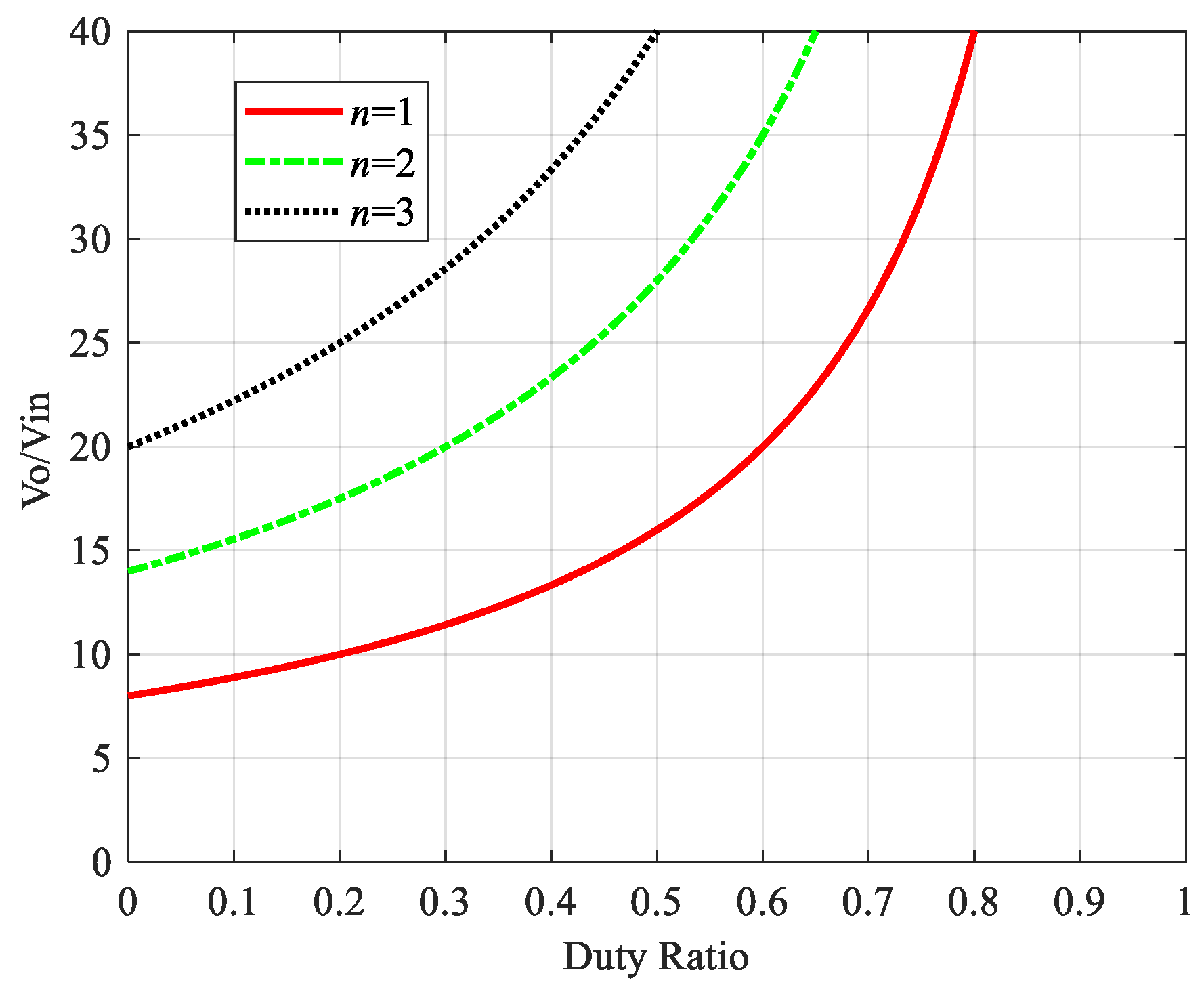
The different curves of voltage gain with turns ratio n = 1, and various coupling coefficients, k = 1, 0.95, 0.9, are shown in Figure 5. Clearly, the coupling coefficient k has little influence on the voltage gain. If the leakage inductor is ignored (the coupling coefficient k = 1), then the ideal voltage gain of the proposed converter is written in the form
M = V o V i n = 6 n + 2 1 D
From Equation (27), it can be concluded that the voltage gain of the proposed converter has two degrees of design freedom, turns ratio n and duty ratio D. The high voltage gain of the proposed converter can be accomplished without an extremely large duty ratio if the designer selects the appropriate turns ratio of the coupled inductor. The voltage gain curves related to the turns ratio and the duty ratio are plotted in Figure 6. In fact, one can see that the voltage gain was 20 times with duty ratio D = 0.6 and turns ratio n = 1. Thus, the presented topology is suitable for high step-up voltage conversion.

3.2. Voltage Stress Analysis

Based on the operational principle of the presented topology, the voltage stress on switches S 2 and S 1 can be determined by stage 3 and by stage 7, respectively. With the help of Equation (27), the switch voltage stress is given by
V S 2 = V C f = 1 1 D V i n = 1 6 n + 2 V o
V S 1 = V C 1 V C f = 1 1 D V i n = 1 6 n + 2 V o
The switch voltage stress is much smaller than the output voltage. Therefore, MOSFETs with low rated voltage and low on-resistance RDS(ON) can be used to reduce the conduction losses. Moreover, the voltage stresses on the following diodes can be obtained from stage 3.
V D o 1 = V C 1 V C f = 1 1 D V i n = 1 6 n + 2 V o
V D o 2 = V C 2 V C 11 = 2 n 1 D V i n = n 3 n + 1 V o
V D 11 = V C 12 = 2 n 1 D V i n = n 3 n + 1 V o
V D 22 = V C 22 = 2 n 1 D V i n = n 3 n + 1 V o
Similarly, the voltage stresses on the following diodes can be obtained from stage 7.
V D c = V C 1 = 2 1 D V i n = 1 3 n + 1 V o
V D 12 = V C 12 = 2 n 1 D V i n = n 3 n + 1 V o
V D 21 = V C 22 = 2 n 1 D V i n = n 3 n + 1 V o
V D o 3 = V C 3 V C 21 = 2 n 1 D V i n = n 3 n + 1 V o
From the results in Equations (30)–(37), the voltage stresses on the diodes are much lower than the output voltage. Therefore, the designer can choose the low forward voltage drop diodes to reduce conduction losses. It is known that the voltage stress on the switch or diode in the interleaved boost converter is equal to the output voltage. Thus, the presented converter has the merit of low semiconductor voltage stress.

3.3. Design Consideration

3.3.1. Considerations of Coupled Inductor Design

If an appropriate duty ratio is selected, then the turns ratio of the coupled inductor can be calculated according to Equation (27) and is given by
n = V o ( 1 D ) 6 V i n 1 3
In order to operate under CCM and current-ripple considerations, the magnetizing inductor of the coupled inductor is designed as follows. If the average current through the magnetizing inductor is denoted as I L m and its ripple current is denoted as Δ i L m , then, the condition for the presented converter operating in CCM can be represented as
I L m   >   1 2 Δ i L m
Based on the operational principle, the ripple current Δ i L m can be expressed as
Δ i L m = V i n L m D T s
where T s is the switching period. The average current I L m can be written in the form
I L m = P o 2 V i n
where P o denotes the output power. Therefore, the value of the magnetizing inductor L m must satisfy the following condition in CCM operation.
L m > V i n 2 D T s P o
Substituting Equation (27) into Equation (42), we obtain
L m > 1 D 2 V o 2 D T s 6 n + 2 2 P o = D 1 D 2 R o 6 n + 2 2 f s
where f s is the switching frequency.

3.3.2. Considerations regarding Capacitor Design

The main consideration regarding each capacitor is suppression of the voltage ripple to an acceptable level. According to the operational principle of the presented converter, the output capacitor C 1 discharges to the load by the output current in a total time of about D T s . Therefore, the ripple voltage on the output capacitor C 1 can be expressed as
Δ V C 1 D V o R o C 1 f s
Substituting Equations (11) and (27) into Equation (44), we obtain
Δ V C 1 = ( 3 n + 1 ) D V C 1 R o C 1 f s
If the specification of the voltage ripple on the output capacitor C 1 is provided, then the design condition of the output capacitor C 1 can be given by
C 1 = ( 3 n + 1 ) D R o f s ( Δ V C 1 / V C 1 )
Similarly, if the percentage of voltage ripple is specified, then the design conditions of the output capacitors C 2 and C 3 can be, respectively, expressed as
C 2 = ( 6 n + 2 ) D 3 n R o f s ( Δ V C 2 / V C 2 )
C 3 = ( 6 n + 2 ) D 3 n R o f s ( Δ V C 3 / V C 3 )
The average charging current i ¯ C 11 ( charge ) of the regenerative capacitor C 11 in one switching period is equal to the average current i ¯ D 11 of the regenerative diode D 11 . By applying the amp-second balance principle, the design condition of capacitor C 11 can be expressed as
C 11 = ( 6 n + 2 ) n R o f s Δ V C 11 / V C 11
The average discharging current i ¯ C 12 ( discharge ) of the voltage-doubler capacitor C 12 in one switching period is equal to the average current i ¯ D o 1 of the output diode D o 1 . In a similar way to that of the design method of C 11 , the design condition of the capacitance and the voltage ripple can be derived by
C 12 = ( 6 n + 2 ) 2 n R o f s Δ V C 12 / V C 12
Similarly, the values of the capacitors C 21 and C 22 can be, respectively, derived by
C 21 = ( 6 n + 2 ) n R o f s Δ V C 21 / V C 21
C 22 = ( 6 n + 2 ) 2 n R o f s Δ V C 22 / V C 22

3.4. Converter Performance Comparison

In order to illustrate the performance of the presented converter, a comparison to the similar interleaved high voltage gain DC-DC converters published in [28,29,30,31,32,33] is shown in Table 1. If the turns ratio was n 1 (the general case for high voltage gain purposes), it revealed the following results: (1) the voltage conversion ratio of the presented converter was the highest; (2) the switch voltage stress of the presented converter was the lowest, and was much lower than the output voltage; (3) the maximum diode voltage stress of the presented converter was the lowest, and was much lower than the output voltage; (4) the number of components was not the largest.
The voltage gain of the presented converter was higher than that of the converter in [33] if the turns ratio was n > 1. The switches turned on under the ZCS condition to reduce the switching losses in the proposed converter. The converter in [33] had the advantage of fewer components; however, the switches did not have the ZCS turn-on feature.

4. Driving Circuit and Controller Design

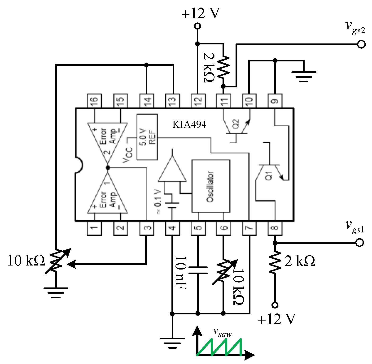
The converter operates in an interleaved mode. It was necessary to design a driving circuit to generate PWM signals with a phase shift of 180 ° to drive the power switches. The driving circuit implemented by the PWM IC KIA494 is shown in Figure 7.
In order to keep the output voltage at a specific value, regardless of input voltage fluctuations and load changes, the closed-loop control system, shown in Figure 8, was employed to obtain good output voltage regulation. In the block diagram, C ( s ) is the controller transfer function and 1 / V P is the pulse-width modulator (PWM) gain, where V P is the amplitude of sawtooth waveform in the PWM. Function P ( s ) is the small signal transfer function of the presented converter from the duty ratio to the output voltage and K is the sensor gain of the output voltage. The controller C ( s ) required a design such that the open-loop transfer function T O L ( s ) met the following specifications:
  • A gain crossover frequency of 1 kHz ( 2 π × 10 3 rad / s ).
  • A phase margin (P.M.) larger than 50 o .
  • The low frequency gain of the open-loop transfer function T O L ( s ) to be very high to reduce the steady-state error for the constant reference input.
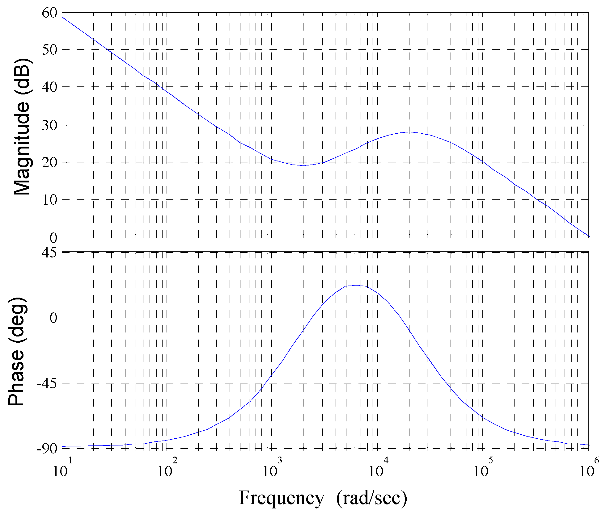
The frequency response analyzer NF FRA51602 was used to measure the frequency response from the control signal v ˜ c t r l to the output voltage sensing signal K v ˜ o at the operating point of the proposed converter. Then, the curve fitting method, using the MATLAB software, was employed to establish the transfer function of G ( s ) , where
G ( s ) = K v ˜ o ( s ) v ˜ c t r l ( s ) = K V p P ( s )
The transfer function by the curve-fitting method is obtained by
G s = k v ˜ o ( s ) v ˜ c t r l ( s ) = 1 . 54 1 + 2 . 2 1400 s + 1 1400 2 s 2
The Bode plots of the measured method and the curve-fitting method are shown together in Figure 9. From the comparison, it can be seen that the curves were quite consistent for the frequency range concerned. Consequently, the transfer function given in Equation (54) was utilized to design the controller.
In this article, the K factor approach [34] was employed to design the well-known Type III controller. The electronic circuit with six passive components is illustrated in Figure 10, and the circuit transfer function is expressed by
v ˜ c t r l ( s ) K v ˜ o ( s ) = R 1 + R 3 R 1 R 3 C 2 s + 1 R 2 C 1 s + 1 ( R 1 + R 3 ) C 3 s s + 1 R 2 C 1 C 2 / ( C 1 + C 2 ) s + 1 R 3 C 3
The controller consists of an integrator and two sets of phase leaders. The integrator is helpful to ensure a steady-state error of zero. The phase leaders are helpful to provide enough phase margin to keep the control loop stable. The controller transfer function was designed and obtained as
C s = 1 . 13 × 10 6 ( s + 2024 ) ( s + 1761 ) s ( s + 24380 ) ( s + 20903 )
with the parameters of the six components:
R 1 = 100   k Ω , R 2 = 426   k Ω , R 3 = 9.2   k Ω ,   C 1 = 1.16   nF , C 2 = 0.105   nF , C 3 = 5.2   nF
The frequency response of the controller C ( s ) is shown in Figure 11.
The frequency response of the open-loop transfer function T O L ( s ) = C ( s ) G ( s ) was obtained as depicted in Figure 12. The control system provides a gain crossover frequency of ω = 2 π × 10 3 rad/s, a phase margin of 50 o , and very high DC gain. Thus, the designed controller satisfies the specification requirements of the voltage control system.

5. Experimental Results

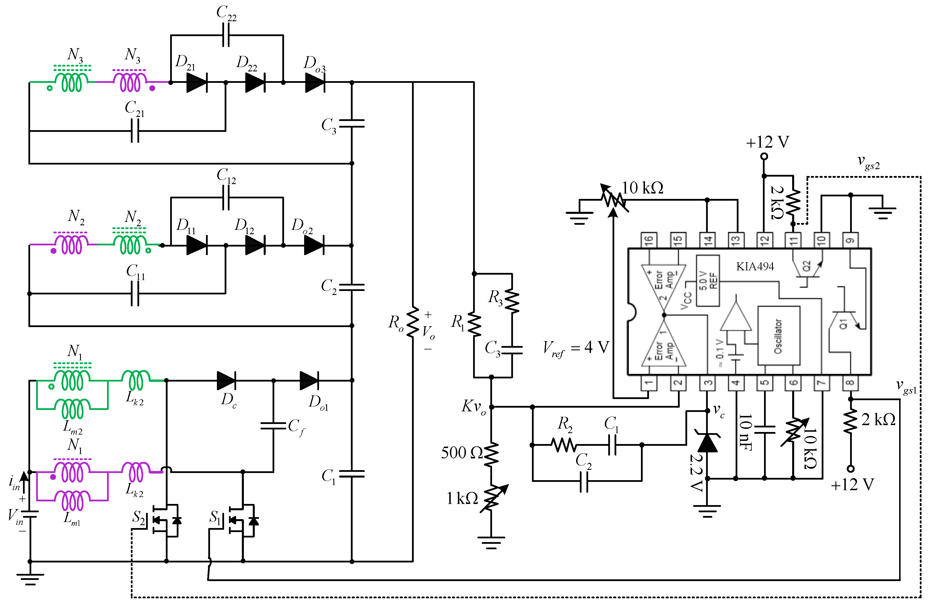
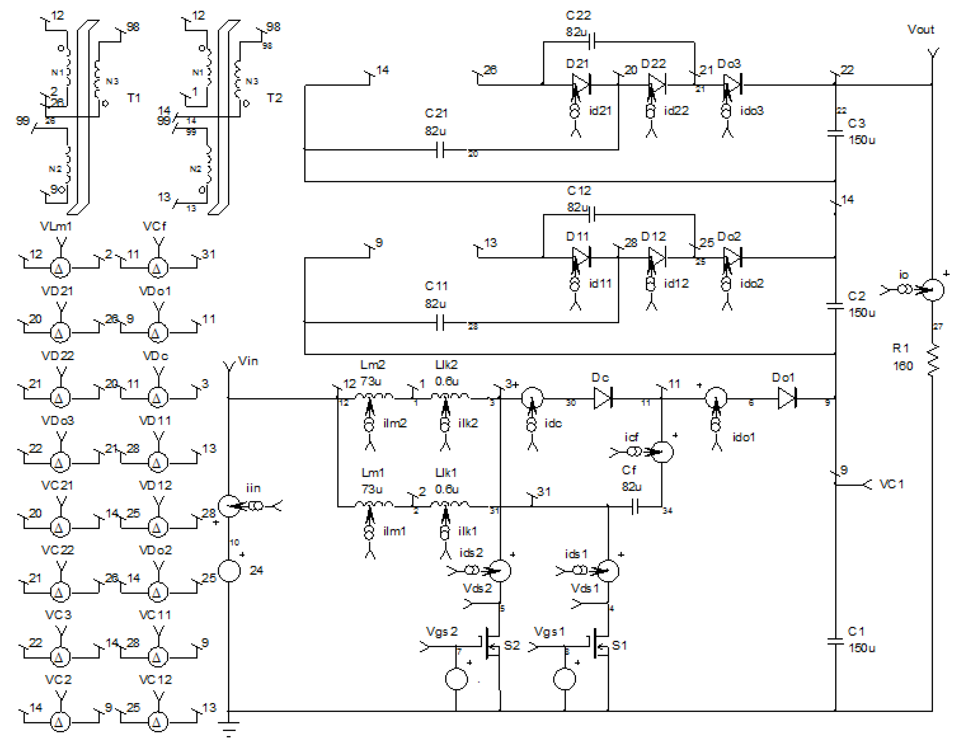
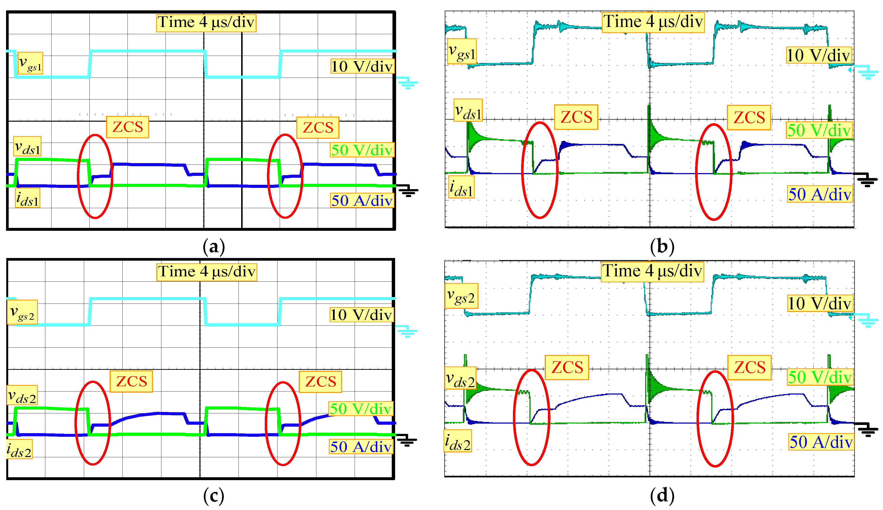
A 1000 W laboratory prototype, with voltage conversion from 24 V to 400 V, was implemented and tested to validate the performance of the presented converter. The detailed and complete circuit of the experiment with the closed-loop control is shown in Figure 13. The sensor gain K of the output voltage was equal to 1/100 in the closed-loop control system. Therefore, the reference signal Vref was equal to 4 V. Figure 14 shows the prototype photograph. The components and parameters of the experimental converter are shown in Table 2. The simulation of the proposed converter was performed by the circuit simulation software Is-Spice, with the circuit shown in Figure 15. The Under the full load (1000 W) condition, the simulated results and the experimental results are demonstrated in Figure 16, Figure 17, Figure 18, Figure 19, Figure 20, Figure 21, Figure 22, Figure 23 and Figure 24.
The waveforms of the gating signals v g s 1 and v g s 2 of the switches, output voltage and input voltage are illustrated in Figure 16. The voltage conversion ratio was over 16 times with V o = 400 V and V i n = 24 V . It was verified that the converter achieved high voltage gain without a very large duty ratio.
Figure 17 illustrates the waveforms of the gating signals and the switch voltages v d s 1 and v d s 2 . The maximum switch voltage was slightly more than 50 V. The switch voltage stress was much lower than the output voltage 400 V. Clearly, the switches of the proposed converter had low voltage stress.
The waveforms of the input current i i n , the leakage currents i L k 1 and i L k 2 are shown in Figure 18. The input parallel structure of two-phase shares the input current to reduce the current stress of power devices. On the other hand, the ripple currents of i L k 1 and i L k 2 were almost the same, with an amplitude of 49 A. The current ripple cancellation was achieved, due to the interleaved operation, such that the ripple current of i i n reduced to only 2 A. It was verified that the interleaved operation could reduce the input current ripple for the parallel input structure.
The current and voltage waveforms of the regenerative diodes D 11 and D 21 , as well as those of the voltage-doubler diodes D 12 and D 22 , are shown in Figure 19 and Figure 20, respectively. It can be seen that there were no reverse-recovery currents, due to the ZCS turn-off feature. The voltage stresses were equal to 100 V, which was only one-fourth of the output voltage. The measured results agreed with the analyzed results.
Figure 21 shows the switch current and voltage waveforms. The switch currents i d s 1 and i d s 2 rose linearly from 0 when each switch began to conduct. The ZCS turn-on performance was achieved to reduce the switching losses.
The voltage waveforms of the output capacitors C 1 , C 2 and C 3 are shown in Figure 22. The voltage V C 1 was slightly more than 100 V and the voltages V C 2 and V C 2 were about 150 V, which was in keeping with the results of the analysis. The simulation results were consistent with the experimental results.
Figure 23a shows the output voltage response and the input voltage variation between 24 V and 27 V. On the other hand, the output voltage response and the output current under the step-on and step-off load changes between 500 W and 1000 W are illustrated in Figure 23b. As shown in the figures, the transient ripples of output voltage were clearly very small. The results demonstrated good voltage regulation performance, due to the well-designed controller, for the closed-loop control system.
The measured efficiency of the prototype converter at different output powers is illustrated in Figure 24. The highest efficiency was 95.52% at 200 W, and the efficiency at 1000 W full load was 87.36%.

6. Conclusions

By applying the three-winding coupled-inductor technique, a new high voltage gain interleaved DC–DC converter for renewable energy systems is introduced in this paper. The voltage gain is further extended and the semiconductor voltage stresses are reduced by the voltage multiplier modules. The principle of operation, steady-state analysis, design considerations and controller design are presented. The high voltage conversion ratio is accomplished without a very large duty ratio. The designer can adopt low on-state resistance MOSFETs and low forward voltage drop diodes to reduce the conduction losses, due to their low voltage stresses. With the help of the leakage inductors of the coupled-inductors, the ZCS condition turn-on is intrinsically provided for the switches. The interleaved operation reduces the input current ripple. The leakage energy is recycled to eliminate the voltage spikes on the switches. A performance comparison with other similar converters was carried out to reveal the merits of the introduced converter. Moreover, a closed-loop controller was designed and implemented to ensure effective output voltage regulation. Finally, the simulation and experimental results, using a 1000 W prototype, are provided to validate the derived analysis and to demonstrate the advantages of the presented converter. Thus, the proposed DC-DC converter with high voltage gain and high efficiency is suitable for renewable energy systems.

Author Contributions

This paper was a collaborative work of all the authors. Conceptualization, S.-J.C. and S.-P.Y.; methodology, S.-J.C. and C.-M.H.; software, P.-S.H.; Investigation, S.-J.C. and S.-P.Y.; validation, S.-J.C., S.-P.Y. and P.-S.H.; writing—original draft preparation, S.-J.C.; supervision, C.-M.H. All authors have read and agreed to the published version of the manuscript.

Funding

This research was funded by the National Science and Technology Council, Taiwan, under grant No. MOST 111-2637-E-168-002.

Data Availability Statement

Not applicable.

Conflicts of Interest

The authors declare no conflict of interest.

References

  1. Nouri, T.; Nouri, N.; Vosoughi, N. A novel high step-up high efficiency interleaved DC-DC Converter with coupled inductor and built-in transformer for renewable energy systems. IEEE Trans. Ind. Electron. 2020, 67, 6505–6516. [Google Scholar] [CrossRef]
  2. Tofoli, F.L.; Pereira, D.C.; Paula, W.J.; Junior, D.S.O. Survey on non-isolated high-voltage step-up DC–DC topologies based on the boost converter. IET Power Electron. 2015, 8, 2044–2057. [Google Scholar] [CrossRef]
  3. Kothapalli, K.R.; Ramteke, M.R.; Suryawanshi, H.M.; Reddi, N.K.; Kalahasthi, R.B. A coupled inductor based high step-up converter for dc microgrid applications. IEEE Trans. Ind. Electron. 2021, 68, 4927–4940. [Google Scholar] [CrossRef]
  4. Liu, H.; Hu, H.; Wu, H.; Xing, Y.; Batarseh, I. Overview of high-step-up coupled-inductor boost converters. IEEE Trans. Power Electron. 2016, 4, 689–704. [Google Scholar] [CrossRef]
  5. Azizkandi, M.E.; Sedaghati, F.; Shayeghi, H.; Blaabjerg, F. Two- and three-winding coupled-inductor based high step-up DC-DC converters for sustainable energy applications. IET Power Electron. 2020, 13, 144–156. [Google Scholar] [CrossRef]
  6. Pereira, A.V.C.; Cavalcanti, M.C.; Azevedo, G.M.; Bradaschia, F.; Neto, R.C.; Carvalho, M.R.S. A novel single-switch high step-up dc–dc converter with three-winding coupled inductor. Energies 2021, 14, 6288. [Google Scholar] [CrossRef]
  7. Li, W.; Zhao, Y.; Wu, J.; He, X. Interleaved high step-up converter with winding-cross-coupled inductors and voltage multiplier cells. IEEE Trans. Power Electron. 2012, 27, 133–143. [Google Scholar] [CrossRef]
  8. Barbosa, E.A.O.; Carvalho, M.R.S.; Limongi, L.R.; Cavalcanti, M.C.; Barbosa, E.J.; Azevedo, G.M.S. High-gain high-efficiency DC-DC converter with single-core parallel operation switched inductors and rectifier voltage multiplier cell. Energies 2021, 14, 4634. [Google Scholar] [CrossRef]
  9. Schmitz, L.; Martins, D.C.; Coelho, R.F. Comprehensive conception of high step-up DC-DC converters with coupled inductor and voltage multiplier techniques. IEEE Trans. Circuits Syst. 2020, 67, 2140–2151. [Google Scholar] [CrossRef]
  10. Alzahrani, A.; Ferdowsi, M.; Shamsi, P. A Family of scalable non-isolated interleaved DC-DC boost converters with voltage multiplier cells. IEEE Access 2019, 7, 11707–11721. [Google Scholar] [CrossRef]
  11. Andrade, A.M.; Mattos, E.; Schuch, L.; Hey, H.L.; Martions, M.L.D.S. Synthesis and comparative analysis of very high step-up DC-DC converters adopting coupled-inductor and voltage multiplier cells. IEEE Trans. Power Electron. 2018, 33, 5880–5897. [Google Scholar] [CrossRef]
  12. Nouri, T.; Vosoughi, N.; Hosseini, S.H.; Babaei, E.; Sabahi, M. An interleaved high step-up converter with coupled inductor and built-in transformer voltage multiplier cell techniques. IEEE Trans. Ind. Electron. 2019, 66, 1894–1905. [Google Scholar] [CrossRef]
  13. Guepfrih, M.F.; Waltrich, G.; Lazzarin, T.B. High step-up DC–DC converter using built-in transformer voltage multiplier cell and dual boost concepts. IEEE J. Emerg. Sel. Top. Power Electron. 2021, 9, 6700–6712. [Google Scholar] [CrossRef]
  14. Tang, Y.; Fu, D.; Wang, T.; Xu, Z. Hybrid switched-inductor converters for high step-up conversion. IEEE Trans. Ind. Electron. 2015, 62, 1480–1490. [Google Scholar] [CrossRef]
  15. Andrade, J.M.; Coelho, R.F.; Lazzarin, T.B. High step-up DC–DC converter based on modified active switched-inductor and switched-capacitor cells. IET Power Electron. 2020, 13, 3127–3137. [Google Scholar] [CrossRef]
  16. Salvador, M.A.; Lazzarin, T.B.; Coelho, R.F. High step-up DC-DC converter with active switched-inductor and passive switched-capacitor networks. IEEE Trans. Ind. Electron. 2018, 65, 5644–5654. [Google Scholar] [CrossRef]
  17. Salvador, M.A.; Andrade, J.M.; Lazzarin, T.B.; Coelho, R.F. Nonisolated high-step-up DC-DC converter derived from switched-inductors and switched-capacitors. IEEE Trans. Ind. Electron. 2020, 67, 8506–8516. [Google Scholar] [CrossRef]
  18. Duong, T.D.; Nguyen, M.K.; Tran, T.T.; Lim, Y.C.; Choi, J.H. Transformer-less switched-capacitor quasi-switched boost DC-DC converter. Energies 2021, 14, 6591. [Google Scholar] [CrossRef]
  19. Taghavi, S.S.; Rezvanyvardom, M.; Mirzaei, A.; Gorji, S.A. High step-up three-level soft switching DC-DC converter for photovoltaic generation systems. Energies 2023, 16, 41. [Google Scholar] [CrossRef]
  20. Rodrigues, J.P.; Mussa, S.A.; Barbi, I.; Perin, A.J. Three-level zero-voltage switching pulse-width modulation DC-DC boost converter with active clamping. IET Power Electron. 2010, 3, 345–354. [Google Scholar] [CrossRef]
  21. He, L.; Xu, X.; Chen, J.; Sun, J.; Guo, D.; Zeng, T. A plug-play active resonant soft switching for current-autobalance interleaved high step-up DC-DC converter. IEEE Trans. Power Electron. 2019, 34, 7603–7616. [Google Scholar] [CrossRef]
  22. Eskandari1, R.; Babaei, E.; Sabahil, M.; Ojaghkandi, S.R. Interleaved high step-up zero-voltage zero current switching boost DC-DC converter. IET Power Electron. 2020, 13, 96–103. [Google Scholar] [CrossRef]
  23. Khorasani, R.R.; Jazi, H.M.; Chaudhuri, N.R.; Sadigh, A.K.; Shaneh, M. An interleaved soft switched high step-up boost converter with high power density for renewable energy applications. IEEE Trans. Power Electron. 2022, 37, 13782–13798. [Google Scholar] [CrossRef]
  24. Carvalho, M.R.S.; Neto, R.C.; Barbosa, E.J.; Limongi, L.R.; Bradaschia, F.; Cavalcanti, M.C. An overview of voltage boosting techniques and step-up DC-DC converters topologies for pv applications. Energies 2021, 14, 8230. [Google Scholar] [CrossRef]
  25. Arunkumari, T.; Indragandhi, V. An overview of high voltage conversion ratio DC-DC converter configurations used in DC micro-grid architectures. Renew. Sustain. Energy Rev. 2017, 77, 670–687. [Google Scholar] [CrossRef]
  26. Forouzesh, M.; Siwakoti, Y.P.; Gorji, S.A.; Lehmen, B. Step-up DC-DC comprehensive review of voltage-boosting techniques, topologies, and applications. IEEE Trans. Ind. Electron. 2017, 32, 9143–9178. [Google Scholar] [CrossRef]
  27. Guan, Y.; Cecati, C.; Alonso, J.M.; Zhang, Z. Review of high-frequency high-voltage-conversion-ratio DC-DC converters. IEEE Trans. Ind. Electron. 2021, 2, 374–389. [Google Scholar] [CrossRef]
  28. Nouri, T.; Hosseini, S.H.; Babaei, E.; Ebrahimi, J. Interleaved high step-up DC-DC converter based on three-winding high-frequency coupled inductor and voltage multiplier cell. IET Power Electron. 2015, 8, 175–189. [Google Scholar] [CrossRef]
  29. He, L.; Liao, Y. An advanced current-autobalance high step-up converter with a multicoupled inductor and voltage multiplier for a renewable power generation system. IEEE Trans. Power Electron. 2016, 31, 6992–7005. [Google Scholar]
  30. Chen, S.J.; Yang, S.P.; Huang, C.M.; Chou, H.M.; Shen, M.J. Interleaved high step-up DC-DC converter based on voltage multiplier cell and voltage-stacking techniques for renewable energy applications. Energies 2018, 11, 1632. [Google Scholar] [CrossRef]
  31. Salehi, S.M.; Dehghan, S.M.; Hasanzadeh, S. Interleaved-input series output ultra-high voltage gain DC-DC converter. IEEE Trans. Power Electron. 2019, 34, 3397–3406. [Google Scholar] [CrossRef]
  32. Chen, S.J.; Yang, S.P.; Huang, C.M.; Chen, Y.H. Interleaved high step-up DC-DC converter with voltage-lift and voltage-stack techniques for photovoltaic systems. Energies 2020, 13, 2537. [Google Scholar] [CrossRef]
  33. Rahimi, R.; Habibi, S.; Ferdowsi, M.; Shamsi, P. A three-winding coupled inductor-based interleaved high-voltage gain DC-DC converter for photovoltaic systems. IEEE Trans. Power Electron. 2022, 37, 990–1002. [Google Scholar] [CrossRef]
  34. Venable, D. The K factor: A new mathematical tool for stability analysis and synthesis. Proc. Powercon 1983, 10, 1–12. [Google Scholar]
Figure 1. A renewable energy system.
Energies 16 03958 g001
Figure 2. (a) Proposed high voltage gain DC–DC converter. (b) Equivalent circuit.
Energies 16 03958 g002
Figure 3. Key steady-state waveforms.
Energies 16 03958 g003
Figure 4. Operational stages.
Energies 16 03958 g004
Figure 5. Voltage gain curves related to coupling coefficient (n = 1).
Energies 16 03958 g005
Figure 6. Voltage gain curves related to turns ratio (k = 1).
Energies 16 03958 g006
Figure 7. Driving circuit diagram.
Energies 16 03958 g007
Figure 8. Functional block diagram of the feedback system.
Energies 16 03958 g008
Figure 9. Comparison of frequency responses.
Energies 16 03958 g009
Figure 10. Controller circuit.
Energies 16 03958 g010
Figure 11. Frequency response of the controller.
Energies 16 03958 g011
Figure 12. Frequency response of T O L ( s ) .
Energies 16 03958 g012
Figure 13. The complete circuit with feedback control.
Energies 16 03958 g013
Figure 14. Prototype photograph.
Energies 16 03958 g014
Figure 15. Is-spice simulation circuit.
Energies 16 03958 g015
Figure 16. Waveforms of gating signals, output voltage and input voltage: (a) Simulated waveforms; (b) Experimental waveforms.
Energies 16 03958 g016
Figure 17. Waveforms of gate signals and drain-source voltages: (a) Simulated waveforms; (b) Experimental waveforms.
Energies 16 03958 g017
Figure 18. Waveforms of input current and leakage currents: (a) Simulated waveforms; (b) Experimental waveforms.
Energies 16 03958 g018
Figure 19. Current and voltage waveforms of the regenerative diodes: (a) Simulated waveforms; (b) Experimental waveforms.
Energies 16 03958 g019
Figure 20. Current and voltage waveforms of the voltage-doubler diodes: (a) Simulated waveforms; (b) Experimental waveforms.
Energies 16 03958 g020
Figure 21. ZCS soft-switching waveforms of the switches: (a,c) Simulated waveforms; (b,d) Experimental waveforms.
Energies 16 03958 g021
Figure 22. Voltage waveforms of the output capacitors: (a) Simulated waveforms; (b) Experimental waveforms.
Energies 16 03958 g022
Figure 23. Output voltage response. (a) Input voltage variation; (b) Load current change.
Energies 16 03958 g023
Figure 24. Measured efficiency.
Energies 16 03958 g024
Table 1. Performance comparison.
Reference
Converter
[28][29][30][31][32][33]Proposed
Voltage gain 3 n + 1 1 D 2 n + 2 1 D 2 n + 4 1 D 3 n + D ( 2 n 1 ) + 2 1 D 5 n + 1 1 D 4 n + 4 1 D 6 n + 2 1 D
Voltage stress
on switches
V o 3 n + 1 V o 2 n + 2 V o 2 n + 4 V o 3 n + D ( 2 n 1 ) + 2 V o 5 n + 1 V o 4 n + 4 V o 6 n + 2
Maximum diode voltage stress 2 n V o 3 n + 1 2 n + 1 V o 2 n + 2 n V o n + 2 ( n + 1 ) V o 3 n + D ( 2 n 1 ) + 2 2 n V o 5 n + 1 2 n + 1 V o 2 n + 2 n V o 3 n + 1
Number
of switches
2222222
Number
of diodes
8669758
Number
of capacitors
7568658
Number of
coupled inductor
2222222
Voltage gain n = 1 , D = 0 . 6 10101514152020
Table 2. Parameters of prototype converter.
ComponentsParameters
Magnetizing inductors L m 1 , L m 2 73   μ H
Leakage inductors L k 1 , L k 2 0.6   μ H
Turns ratio of coupled inductor n 1
Voltage-lift capacitor C f 82   μ F
Output capacitors C 1 , C 2 , C 3 150   μ F
Regenerative capacitors C 11 , C 21 82   μ F
Voltage-doubler capacitors C 12 , C 22 82   μ F
Switching frequency f s 50   kHz
Switches S 1 , S 2 FDP036N10A
Diodes D 11 , D 21 , D 12 , D 22 , D o 2 , D o 3 V30120C
Diodes D c , D o 1 30CPQ200
Disclaimer/Publisher’s Note: The statements, opinions and data contained in all publications are solely those of the individual author(s) and contributor(s) and not of MDPI and/or the editor(s). MDPI and/or the editor(s) disclaim responsibility for any injury to people or property resulting from any ideas, methods, instructions or products referred to in the content.