Review

Common Architectures and Devices for Current Source Inverter in Motor-Drive Applications: A Comprehensive Review

1
Department of Science and Methods for Engineering, University of Modena and Reggio Emilia, 42121 Reggio Emilia, Italy
2
Key Laboratory of More Electric Aircraft Technology of Zhejiang Province, University of Nottingham Ningbo China, Ningbo 315100, China
*
Author to whom correspondence should be addressed.
Energies 2023, 16(15), 5645; https://doi.org/10.3390/en16155645
Submission received: 21 June 2023 / Revised: 24 July 2023 / Accepted: 25 July 2023 / Published: 27 July 2023
(This article belongs to the Special Issue Advanced Application of Power Electronics in Power Systems)

Abstract

:
When compared to the much more common voltage-source inverter (VSI), the current-source inverter (CSI) is rarely used for variable speed drive applications, due to its disadvantages: the need of a constant DC-link current, typically realized with a front-end converter, and the need for reverse-voltage blocking (RVB) devices, typically implemented with in-series diodes. This limits the overall efficiency of the architecture. This paper investigates latest progress of the CSI research, with the aim of demonstrating why CSI could come back in the near future. Different architectures based on modern wide-bandgap (WBG) switches are analyzed, with an emphasis on why CSI can be advantageous compared to VSI.

1. Introduction

The popular choice of driving electric motors using variable-speed drives aims to obtain a better overall efficiency, which is crucial considering that more than half of globally consumed electricity is used for electric motor systems [1]. Currently, variable-speed drives are usually based on the well known voltage-source inverter (VSI) topology, due to its simplicity and efficiency. Current source inverter (CSI) needs reverse-voltage blocking (RVB) switches and, historically, during the 1960s and 1970s, thyristors and gate turn-off thyristors were used [2].
However, with the advent of fast-switching non-RVB silicon MOSFET and IGBT, CSI lost its popularity, and VSI took its place on market. Although CSI based on thyristor is still used today for particularly high-power (in the order of MW) slow-dynamic applications [3,4,5,6,7], CSI based on MOSFET and IGBT typically needs an additional in-series diode to every switching device to provide RVB capability, which increases the overall cost and conduction losses [3,8,9]. Moreover, CSI needs a constant current source, which is typically obtained with a pre-stage [2], typically containing a bulky inductor. Considering in-series diode and pre-stage, CSI topology is less efficient and more complex than VSI topology [10,11,12]. However, as shown in [9], an electric drive based on CSI may, in niche applications like electric aircraft [13,14,15] and electric engines [16,17,18], represent the best design choice at the system level: the weight and volume of the power converter is higher then an equivalent VSI, but the size of the electric motor results lower. As reported in [9], the design of three electrical machines for an aerospace environmental control system (ECS) with 25 kW of rated power, 270 V of DC-link voltage (common to modern aircraft like Airbus A380 or Boeing 787), and a maximum speed of 25,000 rpm is done. Two machines are fed by VSI without (Machine 1) and with (Machine 2) flux weakening capability, whereas Machine 3 is fed by CSI. The latter fed by CSI shows the highest values of efficiency and power density, making Machine 3 fed by CSI a suitable solution compared to other machines fed by VSI. In particular, thanks to CSI voltage-boosting capability, the CSI shows promise in applications when increasing rated electro-motive forces of the electric machines determines higher system power density. Moreover, CSI has several advantages over VSI, in terms of filtered output voltages, electro-magnetic interferences (EMIs), reliability, and fault-tolerance [3,19,20]. The advent of wide-bandgap (WBG) bi-directional switches poses critical questions when using them in VSI [21], reopening the field for CSI with improved efficiency.
This paper summarizes the most recent progress for CSI topology, and it is subdivided as follows. In Section 2, the typical architecture of a CSI is introduced, as well as CSI7 and CSI with tri-state topology. In Section 3, wide-bandgap based topologies are discussed, thoroughly explaining advantages and problems of new fast-switching devices when used in VSI and CSI.

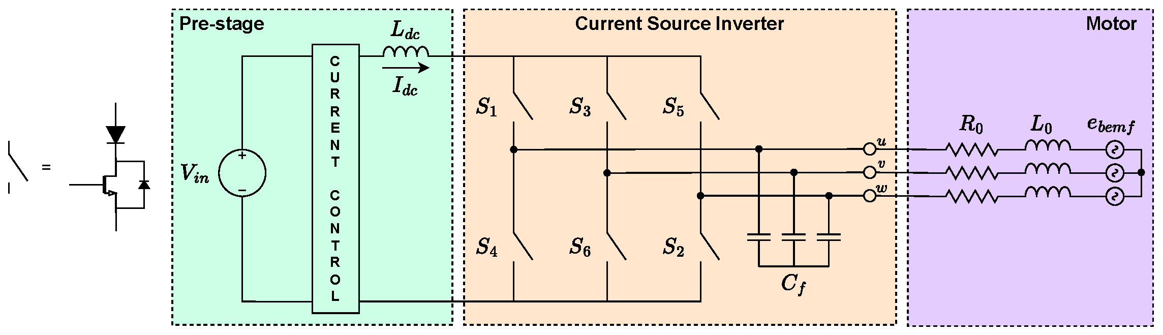
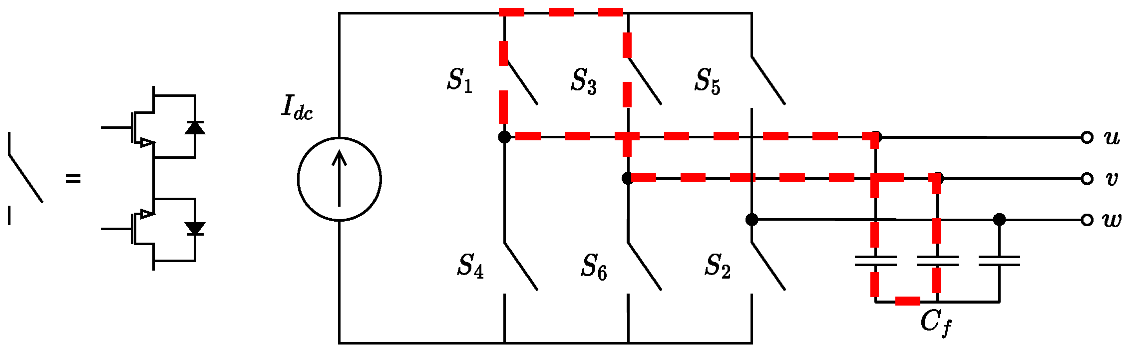
2. Current-Source Inverter: Architecture and Working Principle

The schematic of CSI is shown in Figure 1. The CSI is made up of six unidirectional switches, forming a three-phase bridge, and an output capacitor filter C f to filter high-frequency components of modulated currents. In motor drive applications, it also avoids overvoltages at the motor terminal due to the inductive nature of the load. Inherently, CSI boosts output voltage, hence output phase voltages will be higher than input voltage [22].
The output current I r e f in CSI is obtained by
I r e f = m a I d c
where m a is the amplitude modulation index. The most used modulation technique is space-vector modulation (SVM), based on pulse-width modulation (PWM) and well explained in [2,11,12,23,24]. The base assumption is the presence of a constant current DC-source. Considering Figure 1, nine different combination of on-switches are used, named states. During active states, I d c current flows to the load; during zero states I d c is shunted, as shown in Figure 2a,b.
The states, reported in Table 1, can be represented in fixed reference frame α - β , as shown in Figure 3. The main principle of SVM is that a reference output current I r e f , representing three phase output currents and assumed constant over the sampling period T s , can be synthesized as the sum of two adjacent active states and a zero state. States are imposed for certain dwell times, through the ampere-seconds balancing principle. The resulting dwell times are [2]:
T k = m a sin π 6 θ ( k 1 ) π 3 T s T k + 1 = m a sin π 6 + θ ( k 1 ) π 3 T s T 0 = T s T k T k + 1
where k is the sextant in which I r e f is placed ( k [ 1 , 6 ] , if k = 6 then k + 1 = 1 ), T k and T k + 1 are active state dwell times, and T 0 is zero state dwell time.
From (2), the sum of active and zero dwell times must be equal to T s . The presence of overlap time between states results in an increased zero state dwell time (during overlap is a zero state) and a consequent reduction of active state dwell time, as shown in Figure 4. This causes a distortion in synthesized output current I r e f . Overlap time compensation solutions are discussed in [12,25,26,27]. Two conditions must always be guaranteed to avoid damages on converter devices:
  • There must always be a current path for DC-link inductor current I d c to avoid overvoltage. This is obtained by imposing an overlap time during commutation between states as in Figure 4;
  • There must not be short circuit between output filter capacitors. This is achieved using unidirectional RVB switches, typically obtained with a transistor and an in-series diode, as in Figure 1.
Compared to VSI, CSI has several advantages. Whereas in VSI, output voltages are square waves, output voltages in CSI are quasi-sinusoidal, due to output capacitors C f , forming a second-order low pass filter with the machine inductance L 0 ; this limits motor losses [19], electro-magnetic interference (EMI), and d V / d t problems in motor inter-turn insulation [21]. CSI has higher fault-tolerance, as DC-link inductor limits overcurrent in cases of phase leg shoot-through [28]. The DC-link inductor in CSI is much more robust in terms of vibration, humidity, temperature, and aging than the DC-link capacitor in VSI [29].
On the other hand, typically CSI is less efficient, as in-series diodes cause conduction losses, and it requires more components, as it needs a front-end stage that provides constant I d c . Table 2 summarizes the advantages and disadvantages of VSI and CSI.

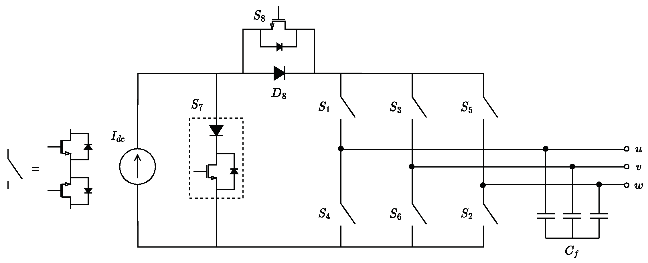
2.1. Seven Switch Topology: CSI7

In [12], a single-stage CSI topology with a seventh switch is presented for grid-connected DC–AC applications and in [10] for electric drives applications, named CSI7.
Figure 5 shows the schematic topology with the seventh switch posed in parallel to the three-phase bridge and used to achieve the zero state. In this way, conduction losses during zero states are halved, and all switches in three-phase bridge achieve zero-current-switching (ZCS) condition. Moreover, this topology with a proper modulation strategy allows for reducing ground leakage current with respect to the classic solution [12]. The boost nature of CSI with a DC voltage source and without a pre-stage power converter limits its operation speed region. At low speed, when back-electro-magnetic force and hence output phase voltages are low, CSI can not operate as a boost. For this reason, the single-stage CSI solution proposed in [10] is able to control the machine phase currents only in the high speed range.

2.2. Seven Switch Topology: CSI with Tri-State

In [30], a solution with tri-state conditions is presented. Tri-state condition is defined by the presence of an additional switch in parallel to L d c choke as in Figure 6.
The tri-state condition allows one to obtain a new free-wheeling state, in which I d c is kept constant and the output currents are equal to zero. Whereas in typical CSI active and zero states are mutually dependent and linked by the relation T k + T k + 1 + T 0 = T s , the new free-wheeling state makes them independent. Thanks to the free-wheeling state, the dynamic performance of power converter control is increased due to the elimination of the right-half-plane (RHP) zero in the control-to-output transfer function.

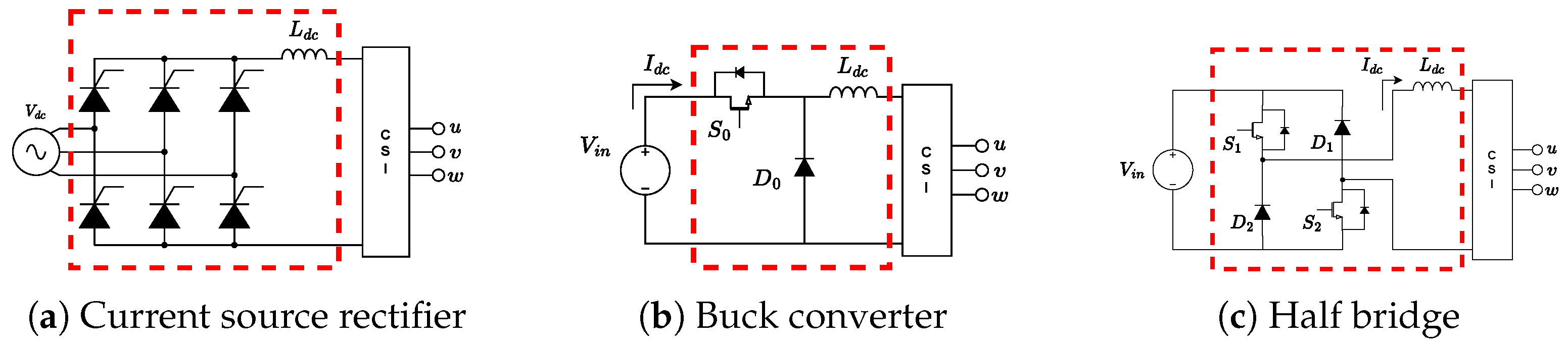
2.3. DC Current Control

CSI needs a constant input current. Because a constant current source is not available, several techniques have been proposed to control DC-link current I d c .
Typically, if an AC voltage source is available, a current source rectifier (CSR) is used [2], as in Figure 7a, whereas if a DC voltage source is available, several different front-end pre-stage have been used. The CSR and the front-end pre-stage also allow CSI to work in buck mode, so that the overall voltage gain can be less than one and output voltage can be lower than input voltage. Furthermore, the CSR can inherently regenerate energy from the motor, allowing bidirectional power flow from and to power source.
In [7], I d c is controlled with a buck (chopper) converter, as in Figure 7b, while the six full-bridge switches are commutated at low frequency with the classical six-step modulation. The switch S 0 controls the current that flows always in two phases of brushless DC motors.
In [28,31] a DC-bidirectional chopper is presented and shown in Figure 7c, which allows current to flow back from load to source, hence regenerative braking. A DC-chopper can operate in three way, allowing current to flow:
  • From power supply to DC-link inductor and load, Figure 8a;
  • From inductor to load, Figure 8b;
  • From load to power supply, Figure 8c;
depending on the states of the chopper switches, as illustrated in Figure 8.
It is possible to control DC-link current I d c even without a pre-stage, when output voltages are desired to be higher than the DC input voltage. In [10], a DC-link current control that does not use any front-end converter was proposed, through a closed loop control of I d c . This is achieved considering that during zero states in SVM, I d c current increases, whereas during active states, it decreases. The control tends to find a modulation index m a so that, for a given working point for motor, I d c remains constant. Although avoiding the use of extra components, this solution does not allow regenerative braking. Moreover, when using a pre-stage, I d c current is typically regulated and minimized so that CSI modulation index is equal to 1. In this way, fewer conduction losses occur. The solution in [10] does not minimize I d c since m a is not set to 1. In any case, the absence of the pre-stage converter can increase converter efficiency.
In Table 3, advantages and disadvantages of shown solutions are summarized, in terms of low speed capability, number of components, and regenerative braking capability. Low speed operation is the ability to drive motor in the low speed region, when output phase voltage is lower than input voltage. The number of components needed is also related to cost and control complexity. Regenerative braking is the ability to restore energy from the motor to the power supply, hence to work in four quadrants.

2.4. Resonance in Motor Drive Application

From Figure 1, the output capacitive filter and motor inductance form a second order CL filter that provides an harmonic suppression of −40 dB per decade [32] and a resonance phenomenon, which could be excited by disturbances. The transfer function of the CSI-PMSM motor plant is shown in [32,33], for example, in Equation (7) of [33]. To ensure system robustness against disturbances, it is important to guarantee enough damping. Looking at the system transfer function, damping is directly proportional to motor winding resistance, so that the simplest way to increase it is to pose in-series passive resistors at the motor input terminal, which cause more losses. A more sophisticated method is active damping. In [33], a virtual resistor is imposed by the feedback controller, so that the system is critically damped, whereas [32] uses a capacitor voltage feedback damping (CVFD) that provides the combination of a virtual resistance and a virtual capacitive reactance extending the previous control. To address the resonance damping, in [34] different control strategies are discussed with a discrete time synthesis. The controls are based on the dynamic capacitor voltage control (DVC) of [35], taking into account the following strategies:
i
Classical FOC control with feedforward decoupling;
ii
Classical FOC control with feedforward decoupling and series active damping;
iii
Classical FOC control with feedforward decoupling and parallel active damping;
iv
Complex vector with decoupling control (based on [36]);
v
Complex vector with decoupling control and series active damping;
vi
Complex vector with decoupling control and parallel active damping.
It has been shown that the use of complex vector with decoupling control and series active damping (v) improves the stability and the dynamic response of the system, ensuring the predefined settling time adopted during the synthesis of the controller. Worst results are obtained with parallel active damping (iii, v) in both situations.

3. Use of Wide-Bandgap Switches

3.1. Properties of Wide-Bandgap Materials

In the last ten years, wide-bandgap (WBG) transistors have become available. WBG materials, such as silicon carbide (SiC) and gallium nitride (GaN), have a higher critical electric field than silicon, which allows one to obtain thinner and more doped semiconductor layers in switching devices. As a consequence, the WBG transistors have smaller on-resistance and parasitic capacitance, ergo lower conduction and switching losses. This leads to the possibility of using higher switching frequency [21,37], thus allowing for the use of smaller passive filtering elements [38] and a higher power density. Moreover, WBG materials can operate at higher temperature. SiC has a thermal conductivity more than three times bigger than silicon [21], which helps in exchanging heat. These characteristics allow for shrinking the size of cooling elements.

3.2. WBG in VSI and CSI

The VSI output voltages are pulsed square waves. High switching frequency and fast output voltage rise/fall times produce a richer harmonic spectrum, i.e., more EMI [39] and overvoltages on the motor terminal due to parasitic cable inductance. Moreover, high d V / d t s stress inter-turn insulation and produce bearing currents, limiting insulation and bearing lifespan [1,3,40]. For these reasons, VSI topology does not permit one to fully exploit the potential of fast WBG switches [21]. It is possible to overcome these problems by limiting switching frequency, only taking advantage of lower on-resistance of WBG-switches or by using an output LC filter. The former may not be economically convenient considering WBG device cost [21], whereas the latter increases the number of components and losses [39], in some cases making VSI converter even worse than CSI in terms of overall efficiency [1,41]. On the contrary, CSI output currents and voltages are quasi-sinusoidal, and this makes CSI an interesting alternative when using WBG switches, being it is inherently immune to the aforementioned problems associated with squared output voltages.
It should be noted that even if high switching frequency allows one to reduce passive elements size, VSI with an output filter is still more compact than CSI [42], mainly due to the bulky DC-link inductor in CSI. However, if the analysis is carried out to the electric drive (power converter and electric machine), this statement cannot always be considered true.

3.3. Improving CSI Performances with WBG Switches

The shrinking in passive and cooling elements given by WBG fast switches opened the interest in integrated motor drive (IMD) systems [1,20,43,44,45,46], limiting size, volume, and cost of converters, eliminating cables and connectors, and exploiting mechanical energy from the motor itself to cool power electronics. IMDs based on CSI topology have the advantage of having the DC-link inductor much more robust than the DC-link capacitor in VSI topology, which is crucial considering a converter enclosed in a motor stator [47].
In [48], normally on SiC JFET switching at 200 kHz is used to develop a CSI. The use of normally on switches assures that, under fault conditions, a natural freewheeling path is available for DC-link inductor current.
As WBG devices are still quite expensive, a cost-effective hybrid SiC and Si seven-switches topology is proposed in [41]. Six Si-switches form a three-phase bridge, while the seventh SiC switch shunts I d c current during commutation between active states, achieving zero states and zero-current-switching (ZCS) conditions for bridge switches. In this way, switching losses are considerably lower than typical Si six-switch CSI. When working at 20 kHz and 3 kW, the proposed solution has a similar efficiency compared to typical VSI with output filter (98.6% vs. 98.5%).
Solutions proposed before still used in-series diodes to obtain RVB switches. In order to remove in-series diodes and achieve better efficiency, efforts have been made to use bi-directional (BD) switches. In [20], a six-BD-switch topology, named H6-CSI, is shown in which every switch is composed of two SiC MOSFETs, connected in common-drain configuration. The use of BD switches increases efficiency, as the voltage drop across the additional switch is lower than across typical in-series diodes, but it poses the problem of inter-phase short circuit during overlap time through the path highlighted in Figure 9, because BD switches are non-reverse blocking.
This commutation problem is solved adopting a 4-step commutation technique, in which the additional transistor body diode is used as a reverse-current blocking diode during commutation, avoiding inter-phase short circuit [20]. Efficiency maps show the efficiency of transistor–diode switch CSI compared to BD switch CSI for different combinations of requested motor speed and torque: efficiency of the latter is about 1% better for every operating point, as fewer conduction losses occur.
In [8], a seven-switch topology, named H7-CSI, is shown in which six BD SiC switches are used, as in [20], and a seventh RVB switch is used to shunt the DC-link current, as in [41]. As result, the six BD switches achieve ZCS conditions and during zero state conduction losses are halved. Efficiency of H7-CSI is higher (between 1% and 3%) than that of H6-CSI.
The disadvantage of the solutions proposed in [20] and [8] is the need of 12 gate drivers for S 1 S 6 , as each BD switch is composed of two transistors. Moreover, the conduction losses during commutation are increased, because the voltage drop across the body diode can be as high as 4V, much higher than in a typical SiC Schottky diode. In [3], an eight-switch topology, named H8-CSI, is proposed and shown in Figure 10. A net composed of diode D 8 and SiC switch S 8 is posed after shunting transistor S 7 . Thanks to S 8 , both transistor forming BD-switches S 1 S 6 can commutate at the same time, without the need of 4-step commutation, limiting the need of gate drivers and eliminating conduction losses on the transistor body diode. H8-CSI is slightly better than H7-CSI in terms of efficiency and requires only 8 gate signals and gate drivers instead of 13.
In [45], the aforementioned topologies H6-, H7-, and H8-CSI are compared when different WBG devices are used in the field of IMD. Transistors tested are C3M0065090J (max. current 35A, SiC), GS66508T (max. current 30A, GaN), and GS66516T (max. current 60A, GaN). As expected, in terms of efficiency, H6-CSI is worse than H7-CSI, which is worse than H8-CSI. From the relation between efficiency and junction temperature, the result is that SiC devices are more insensitive to temperature rise.
The classical solution to minimize conduction losses of a CSI with pre-stage is to choose a modulation index m a equal to 1. DC-link current I d c causes conduction losses even during the zero state. It is therefore possible to avoid zero state when working in buck mode in order to decrease conduction losses. In [49], a CSI topology with a buck pre-stage is presented, similar to the one shown in Figure 7b. To reduce conduction loss when working in buck mode, m a is set equal to 1 to minimize I d c , which is regulated using the pre-stage, but even if m a = 1 , zero states are necessary. The modulation presented in [49] removes zero states when operating in buck mode under certain conditions of modulation index. Zero states produce conduction losses even if no power is transferred to the motor. Removing them results in an 8% reduction in conduction losses and up to an 83% reduction in switching losses.

3.4. WBG: EMI and Common-Mode Voltages Problem

Finally, one problem posed by WBG devices is the increase in generation of EMI [50] and high-frequency common-mode (CM) voltages [39]. In [50], it is shown why WBG devices are EMI sources. Si- and SiC-based converters are compared, showing how the latter emits much higher (20+ dB) conducted and radiated EMIs in the whole analyzed spectrum. In [51], it is thoroughly explained how CM voltage is generated. In [40], a simplified lumped-elements model of a WBG-converter with a motor system including parasitic elements is shown, which is used to derive a transfer function-based analysis for CM voltages. High frequency components of CM voltages are responsible for leakage current, as they excite parasitic capacitive path between the motor winding and ground.
The simplest way to reduce CM voltages is to split input inductance L d c in two equal halves [51], as in Figure 1. Several modulation strategies and soft-switching CSI are then presented, with the aim of reducing CM voltages. The work in [50] shows the active-gate-drive technique to limit the steepness d V / d t on voltage transient and high frequency harmonic content in output voltage. In [52], is shown how zero states in SVM produce the highest peak in CM voltages. Hence two different nonzero-state modulation strategies are presented, based on SVM but avoiding zero states. In active-zero-state modulation, zero states are substituted with opposite active states. In near-three-state modulation, active states are obtained as the sum of three adjacent active states.
It is shown how near-three-state modulation can achieve a 50% decrease in CM voltages. The main disadvantage of these different SVM techniques is the limitation of the modulation index. In [31], an additional shunting net to achieve zero state with zero CM voltage and full modulation index range is proposed.
In [53], an auxiliary resonant circuit is added to DC-link inductor, made of two SiC switches, two diodes, a resonant inductor, and a resonant capacitor. Applying a particular modulation scheme, zero-voltage-switching (ZVS) condition is achieved for bridge switches. Random-switching-frequency technique is also employed to distribute switching harmonics evenly in the spectrum. Compared to hard-switching topology, this random-frequency zero-voltage switching solution has lower EMI over the whole spectrum, especially in the [3, 30] MHz range.

3.5. WBG: Summary of Shown Solutions

Table 4 summarizes advantages and disadvantages of the shown solution, in terms of component count, efficiency, common mode voltages, and complexity (gate driver number and modulation strategy).

4. Conclusions

This paper shows the actual state of the art of electric drives based on a CSI converter. Typical architecture, working principles, advantages, and disadvantages when compared to VSI are shown. To obtain the CSI control in the four quadrants with a DC voltage source, the state-of-the-art solution is based on employing the bi-directional DC-chopper [28,31]. This allows the CSI to work in buck mode and to regenerate energy during braking. It is possible to reduce semiconductor power losses and component counts removing this power stage, as shown in [10], but in this case, the DC-link current control is effective only when the speed of the electric machine allows the CSI to work as a boost.
The advent of WBG devices can improve performance of CSI converters, because they:
  • Reduce semiconductor power loss, thanks to lower on-resistance;
  • Can operate at higher temperatures, allowing one to integrate the motor drive;
  • Allow for increasing switching frequency, hence decreasing the size of passive and cooling elements;
  • Are not suitable for VSI, because of high d V / d t s and EMI issues, which reduce device performance in practical applications.
Different CSI architectures were presented, employing WBG devices to achieve an efficiency comparable to that of VSI. Combining the current control strategy in [10] and WBG devices, one can obtain a CSI comparable to VSI in terms of complexity and efficiency in the field of high-speed motors, where it is not necessary to buck input voltage. There is still the need to explore CSI based solutions that can work at low speed without the need of a pre-stage.
The intrinsic advantages of the CSI—higher reliability and robustness—can guarantee the same features also for the electric machines thanks to output sinusoidal voltages and low ground leakage current. Currently, the power density of CSI is lower with respect to the VSI solution, but if the whole CSI-motor system is considered, this is not true [9].
Considering the advent of WBG and the unmistakable CSI advantage of having motor-friendly output voltages, it is not to be excluded that the system-level advantages of DC-link element robustness and reduced stress on electrical machines may tilt the scale towards the CSI topology rather than the VSI for some applications in harsh environments, like in the field of integrated motor drives and electric aircraft.

Author Contributions

Conceptualization, G.L.F., G.M. and E.L.; methodology, E.L.; formal analysis, G.L.F., G.M., E.C. and G.B.; investigation, G.L.F., G.M., E.C. and G.B.; resources, G.L.F., D.B. and F.I.; writing—original draft preparation, G.L.F., E.C. and G.B.; writing—review and editing, G.M., E.C., D.B., F.I. and G.B.; supervision, E.L. All authors have read and agreed to the published version of the manuscript.

Funding

This research received no external funding.

Data Availability Statement

Data sharing not applicable.

Conflicts of Interest

The authors declare no conflict of interest.

References

  1. Torres, R.A.; Dai, H.; Lee, W.; Jahns, T.M.; Sarlioglu, B. Development of Current-Source-Inverter-based Integrated Motor Drives using Wide-Bandgap Power Switches. In Proceedings of the 2019 IEEE 15th Brazilian Power Electronics Conference and 5th IEEE Southern Power Electronics Conference (COBEP/SPEC), Santos, Brazil, 1–4 December 2019; pp. 1–6. [Google Scholar] [CrossRef]
  2. Wu, B.; Narimani, M. PWM Current Source Inverters. In High-Power Converters and AC Drives; John Wiley & Sons, Ltd.: Hoboken, NJ, USA, 2017; Chapter 10; pp. 225–256. [Google Scholar] [CrossRef]
  3. Dai, H.; Torres, R.A.; Chen, F.; Jahns, T.M.; Sarlioglu, B. An H8 Current-Source Inverter Using Single-Gate WBG Bidirectional Switches. IEEE Trans. Transp. Electrif. 2023, 9, 1311–1329. [Google Scholar] [CrossRef]
  4. Kwak, S.; Kim, T. An Integrated Current Source Inverter with Reactive and Harmonic Power Compensators. IEEE Trans. Power Electron. 2009, 24, 348–357. [Google Scholar] [CrossRef]
  5. Sebastian, C.R.; Rajeevan, P.P. Load-Commutated SCR-Based Current Source Inverter Fed Induction Motor Drive with Open-End Stator Windings. IEEE Trans. Ind. Electron. 2018, 65, 2031–2038. [Google Scholar] [CrossRef]
  6. Beig, A.R.; Ranganathan, V.T. A novel CSI-fed induction motor drive. IEEE Trans. Power Electron. 2006, 21, 1073–1082. [Google Scholar] [CrossRef]
  7. Chen, H.C.; Huang, H.H. Design of buck-type current source inverter fed brushless DC motor drive and its application to position sensorless control with square-wave current. IET Electr. Power Appl. 2013, 7, 416–426. [Google Scholar] [CrossRef]
  8. Dai, H.; Torres, R.A.; Gossmann, J.; Lee, W.; Jahns, T.M.; Sarlioglu, B. A Seven-Switch Current-Source Inverter Using Wide Bandgap Dual-Gate Bidirectional Switches. IEEE Trans. Ind. Appl. 2022, 58, 3721–3737. [Google Scholar] [CrossRef]
  9. Madonna, V.; Migliazza, G.; Giangrande, P.; Lorenzani, E.; Buticchi, G.; Galea, M. The Rebirth of the Current Source Inverter: Advantages for Aerospace Motor Design. IEEE Ind. Electron. Mag. 2019, 13, 65–76. [Google Scholar] [CrossRef]
  10. Migliazza, G.; Buticchi, G.; Carfagna, E.; Lorenzani, E.; Madonna, V.; Giangrande, P.; Galea, M. DC Current Control for a Single-Stage Current Source Inverter in Motor Drive Application. IEEE Trans. Power Electron. 2021, 36, 3367–3376. [Google Scholar] [CrossRef]
  11. Lorenzani, E.; Migliazza, G.; Immovilli, F.; Bianchini, C.; Buticchi, G. Ground Leakage Current in PV Three-Phase Current Source Inverter Topologies. In Proceedings of the 43rd Annual Conference of the IEEE Industrial Electronics Society (IECON 2017), Beijing, China, 29 October–1 November 2017; pp. 4221–4226. [Google Scholar] [CrossRef]
  12. Lorenzani, E.; Immovilli, F.; Migliazza, G.; Frigieri, M.; Bianchini, C.; Davoli, M. CSI7: A Modified Three-Phase Current-Source Inverter for Modular Photovoltaic Applications. IEEE Trans. Ind. Electron. 2017, 64, 5449–5459. [Google Scholar] [CrossRef]
  13. Sayed, E.; Abdalmagid, M.; Pietrini, G.; Sa’adeh, N.M.; Callegaro, A.D.; Goldstein, C.; Emadi, A. Review of Electric Machines in More-/Hybrid-/Turbo-Electric Aircraft. IEEE Trans. Transp. Electrif. 2021, 7, 2976–3005. [Google Scholar] [CrossRef]
  14. Buticchi, G.; Wheeler, P.; Boroyevich, D. The More-Electric Aircraft and Beyond. Proc. IEEE 2023, 111, 356–370. [Google Scholar] [CrossRef]
  15. Madonna, V.; Giangrande, P.; Zhao, W.; Zhang, H.; Gerada, C.; Galea, M. Electrical Machines for the More Electric Aircraft: Partial Discharges Investigation. IEEE Trans. Ind. Appl. 2021, 57, 1389–1398. [Google Scholar] [CrossRef]
  16. Zhang, Y.; Peng, G.O.H.; Banda, J.K.; Dasgupta, S.; Husband, M.; Su, R.; Wen, C. An Energy Efficient Power Management Solution for a Fault-Tolerant More Electric Engine/Aircraft. IEEE Trans. Ind. Electron. 2019, 66, 5663–5675. [Google Scholar] [CrossRef]
  17. Enalou, H.B.; Lang, X.; Rashed, M.; Bozhko, S. Time-Scaled Emulation of Electric Power Transfer in the More Electric Engine. IEEE Trans. Transp. Electrif. 2020, 6, 1679–1694. [Google Scholar] [CrossRef]
  18. Tosetti, M.; Maggiore, P.; Cavagnino, A.; Vaschetto, S. Conjugate Heat Transfer Analysis of Integrated Brushless Generators for More Electric Engines. IEEE Trans. Ind. Appl. 2014, 50, 2467–2475. [Google Scholar] [CrossRef]
  19. Wiechmann, E.P.; Aqueveque, P.; Burgos, R.; Rodriguez, J. On the Efficiency of Voltage Source and Current Source Inverters for High-Power Drives. IEEE Trans. Ind. Electron. 2008, 55, 1771–1782. [Google Scholar] [CrossRef]
  20. Amorim Torres, R.; Dai, H.; Lee, W.; Sarlioglu, B.; Jahns, T. Current-Source Inverter Integrated Motor Drives Using Dual-Gate Four-Quadrant Wide-Bandgap Power Switches. IEEE Trans. Ind. Appl. 2021, 57, 5183–5198. [Google Scholar] [CrossRef]
  21. Morya, A.K.; Gardner, M.C.; Anvari, B.; Liu, L.; Yepes, A.G.; Doval-Gandoy, J.; Toliyat, H.A. Wide Bandgap Devices in AC Electric Drives: Opportunities and Challenges. IEEE Trans. Transp. Electrif. 2019, 5, 3–20. [Google Scholar] [CrossRef]
  22. Sahan, B.; Araújo, S.V.; Nöding, C.; Zacharias, P. Comparative Evaluation of Three-Phase Current Source Inverters for Grid Interfacing of Distributed and Renewable Energy Systems. IEEE Trans. Power Electron. 2011, 26, 2304–2318. [Google Scholar] [CrossRef]
  23. Wei, Q.; Xing, L.; Xu, D.; Wu, B.; Zargari, N.R. Modulation Schemes for Medium-Voltage PWM Current Source Converter-Based Drives: An Overview. IEEE J. Emerg. Sel. Top. Power Electron. 2019, 7, 1152–1161. [Google Scholar] [CrossRef]
  24. Liu, P.; Wang, Z.; Xu, Y.; Zou, Z.; Deng, F.; Li, Y. Improved Harmonic Profile for High-Power PWM Current-Source Converters with Modified Space-Vector Modulation Schemes. IEEE Trans. Power Electron. 2021, 36, 11234–11244. [Google Scholar] [CrossRef]
  25. Geng, Y.; Deng, R.; Dong, W.; Wang, K.; Liu, H.; Wu, X. An Overlap-Time Compensation Method for Current-Source Space-Vector PWM Inverters. IEEE Trans. Power Electron. 2018, 33, 3192–3203. [Google Scholar] [CrossRef]
  26. Gaber, M.; Abdel-Rahim, O.; Orabi, M. Novel Overlap Method to Eliminate Vector Deviation Error in SVM of Current Source Inverters. IEEE Trans. Power Electron. 2021, 36, 2320–2333. [Google Scholar] [CrossRef]
  27. Akbar, F.; Cha, H.; Do, D.T. CSI7: Novel Three-Phase Current-Source Inverter with Improved Reliability. IEEE Trans. Power Electron. 2021, 36, 9170–9182. [Google Scholar] [CrossRef]
  28. Miao, Y.; Liao, W.; Huang, S.; Liu, P.; Wu, X.; Song, P.; Li, G. DC-Link Current Minimization Scheme for IM Drive System Fed by Bidirectional DC Chopper-Based CSI. IEEE Trans. Transp. Electrif. 2022, 9, 2839–2850. [Google Scholar] [CrossRef]
  29. Wang, H.; Blaabjerg, F. Reliability of Capacitors for DC-Link Applications in Power Electronic Converters—An Overview. IEEE Trans. Ind. Appl. 2014, 50, 3569–3578. [Google Scholar] [CrossRef] [Green Version]
  30. Loh, P.C.; Blaabjerg, F.; Wong, C.P.; Tan, P.C. Tri-State Current Source Inverter with Improved Dynamic Performance. IEEE Trans. Power Electron. 2008, 23, 1631–1640. [Google Scholar] [CrossRef]
  31. Xu, Y.; Wang, Z.; Liu, P.; He, J. A Soft-Switching Current-Source-Inverter-Fed Motor Drive with Reduced Common-Mode Voltage. IEEE Trans. Ind. Electron. 2021, 68, 3012–3021. [Google Scholar] [CrossRef]
  32. Yang, S.; Yin, Z.; Tong, C.; Sui, Y.; Zheng, P. Active Damping Current Control for Current-Source Inverter-Based PMSM Drives. IEEE Trans. Ind. Electron. 2023, 70, 3549–3560. [Google Scholar] [CrossRef]
  33. Torres, R.A.; Dai, H.; Lee, W.; Jahns, T.M.; Sarlioglu, B. A Simple and Robust Controller Design for High-Frequency WBG-Based Current-Source-Inverter-Fed AC Motor Drive. In Proceedings of the 2020 IEEE Transportation Electrification Conference & Expo (ITEC), Chicago, IL, USA, 23–26 June 2020; pp. 111–117. [Google Scholar] [CrossRef]
  34. Lee, H.J.; Jung, S.; Sul, S.K. A Current Controller Design for Current Source Inverter-Fed AC Machine Drive System. IEEE Trans. Power Electron. 2013, 28, 1366–1381. [Google Scholar] [CrossRef]
  35. Wang, Z.; Wu, B.; Xu, D.; Zargari, N.R. A Current-Source-Converter-Based High-Power High-Speed PMSM Drive with 420-Hz Switching Frequency. IEEE Trans. Ind. Electron. 2012, 59, 2970–2981. [Google Scholar] [CrossRef]
  36. Briz, F.; Degner, M.; Lorenz, R. Analysis and design of current regulators using complex vectors. IEEE Trans. Ind. Appl. 2000, 36, 817–825. [Google Scholar] [CrossRef] [Green Version]
  37. Shirabe, K.; Swamy, M.; Kang, J.K.; Hisatsune, M.; Wu, Y.; Kebort, D.; Honea, J. Advantages of high frequency PWM in AC motor drive applications. In Proceedings of the 2012 IEEE Energy Conversion Congress and Exposition (ECCE), Raleigh, NC, USA, 15–20 September 2012; pp. 2977–2984. [Google Scholar] [CrossRef]
  38. Kolar, J.W.; Huber, J. Next-Generation SiC/GaN Three-Phase Variable-Speed Drive Inverter Concepts. In PCIM Europe Digital Days 2021; International Exhibition and Conference for Power Electronics, Intelligent Motion, Renewable Energy and Energy Management; VDE VERLAG: Berlin, Germany, 2021; pp. 1–5. [Google Scholar]
  39. Swamy, M.M.; Kang, J.K.; Shirabe, K. Power Loss, System Efficiency, and Leakage Current Comparison Between Si IGBT VFD and SiC FET VFD with Various Filtering Options. IEEE Trans. Ind. Appl. 2015, 51, 3858–3866. [Google Scholar] [CrossRef]
  40. Dai, H.; Jahns, T.M.; Torres, R.A.; Han, D.; Sarlioglu, B. Comparative Evaluation of Conducted Common-Mode EMI in Voltage-Source and Current-Source Inverters using Wide-Bandgap Switches. In Proceedings of the 2018 IEEE Transportation Electrification Conference and Expo (ITEC), Long Beach, CA, USA, 13–15 June 2018; pp. 788–794. [Google Scholar] [CrossRef]
  41. Wang, W.; Gao, F.; Yang, Y.; Blaabjerg, F. Operation and Modulation of H7 Current-Source Inverter with Hybrid SiC and Si Semiconductor Switches. IEEE J. Emerg. Sel. Top. Power Electron. 2018, 6, 387–399. [Google Scholar] [CrossRef]
  42. Riegler, B.; Mütze, A. Volume Comparison of Passive Components for Hard-Switching Current- and Voltage-Source-Inverters. In Proceedings of the 2021 IEEE Energy Conversion Congress and Exposition (ECCE), Vancouver, BC, Canada, 10–14 October 2021; pp. 1902–1909. [Google Scholar] [CrossRef]
  43. Wang, J.; Li, Y.; Han, Y. Integrated Modular Motor Drive Design with GaN Power FETs. IEEE Trans. Ind. Appl. 2015, 51, 3198–3207. [Google Scholar] [CrossRef]
  44. Torres, R.A.; Dai, H.; Lee, W.; Jahns, T.M.; Sarlioglu, B. Current-Source Inverters for Integrated Motor Drives using Wide-Bandgap Power Switches. In Proceedings of the 2018 IEEE Transportation Electrification Conference and Expo (ITEC), Long Beach, CA, USA, 13–15 June 2018; pp. 1002–1008. [Google Scholar] [CrossRef]
  45. Dai, H.; Torres, R.A.; Lee, W.; Jahns, T.M.; Sarlioglu, B. Integrated Motor Drive using Soft-Switching Current-Source Inverters with SiC- and GaN-based Bidirectional Switches. In Proceedings of the 2020 IEEE Energy Conversion Congress and Exposition (ECCE), Detroit, MI, USA, 11–15 October 2020; pp. 2372–2378. [Google Scholar] [CrossRef]
  46. Dai, H.; Jahns, T.M.; Torres, R.A.; Liu, M.; Sarlioglu, B.; Chang, S. Development of High-Frequency WBG Power Modules with Reverse-Voltage-Blocking Capability for an Integrated Motor Drive using a Current-Source Inverter. In Proceedings of the 2018 IEEE Energy Conversion Congress and Exposition (ECCE), Portland, OR, USA, 23–27 September 2018; pp. 1808–1815. [Google Scholar] [CrossRef]
  47. Jahns, T.M.; Sarlioglu, B. The Incredible Shrinking Motor Drive: Accelerating the Transition to Integrated Motor Drives. IEEE Power Electron. Mag. 2020, 7, 18–27. [Google Scholar] [CrossRef]
  48. Friedli, T.; Round, S.D.; Hassler, D.; Kolar, J.W. Design and Performance of a 200-kHz All-SiC JFET Current DC-Link Back-to-Back Converter. IEEE Trans. Ind. Appl. 2009, 45, 1868–1878. [Google Scholar] [CrossRef]
  49. Guacci, M.; Zhang, D.; Tatic, M.; Bortis, D.; Kolar, J.W.; Kinoshita, Y.; Ishida, H. Three-phase two-third-PWM buck-boost current source inverter system employing dual-gate monolithic bidirectional GaN e-FETs. CPSS Trans. Power Electron. Appl. 2019, 4, 339–354. [Google Scholar] [CrossRef]
  50. Zhang, B.; Wang, S. A Survey of EMI Research in Power Electronics Systems with Wide-Bandgap Semiconductor Devices. IEEE J. Emerg. Sel. Top. Power Electron. 2020, 8, 626–643. [Google Scholar] [CrossRef]
  51. Rodriguez, J.; Moran, L.; Pontt, J.; Osorio, R.; Kouro, S. Modeling and analysis of common-mode voltages generated in medium voltage PWM-CSI drives. IEEE Trans. Power Electron. 2003, 18, 873–879. [Google Scholar] [CrossRef] [Green Version]
  52. Zhu, N.; Xu, D.; Wu, B.; Zargari, N.R.; Kazerani, M.; Liu, F. Common-Mode Voltage Reduction Methods for Current-Source Converters in Medium-Voltage Drives. IEEE Trans. Power Electron. 2013, 28, 995–1006. [Google Scholar] [CrossRef]
  53. Wang, Z.; Xu, Y.; Liu, P.; Zhang, Y.; He, J. Zero-Voltage-Switching Current Source Inverter Fed PMSM Drives with Reduced EMI. IEEE Trans. Power Electron. 2021, 36, 761–771. [Google Scholar] [CrossRef]
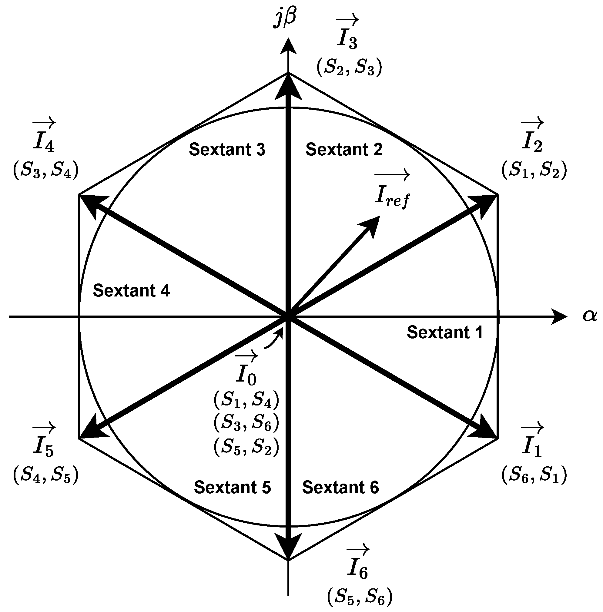
Figure 1. Schematic of a three-phase CSI with pre-stage in motor-drive application.
Energies 16 05645 g001
Figure 2. Examples of active and zero states for CSI.
Energies 16 05645 g002
Figure 3. SVM states in fixed reference frame α - β .
Energies 16 05645 g003
Figure 4. Timing of SVM with insertion of overlap time (red squares).
Energies 16 05645 g004
Figure 5. Schematic of CSI7.
Energies 16 05645 g005
Figure 6. Schematic of tri-state DC-link [30].
Energies 16 05645 g006
Figure 7. Different pre-stage topologies to control DC-link current (in dashed red boxes).
Energies 16 05645 g007
Figure 8. Different operational states and energy flow (in red dashed arrows) for bi-directional DC-chopper.
Energies 16 05645 g008
Figure 9. Interphase short-circuit path (in red dashed lines) when using BD switches.
Energies 16 05645 g009
Figure 10. H8-CSI topology [3].
Energies 16 05645 g010
Table 1. SVM states.
StateVectorON Switch
Active I ¯ 1 S 6 , S 1
I ¯ 2 S 1 , S 2
I ¯ 3 S 2 , S 3
I ¯ 4 S 3 , S 4
I ¯ 5 S 4 , S 5
I ¯ 6 S 5 , S 6
Zero I ¯ 0 S 1 , S 4
S 3 , S 6
S 5 , S 2
Table 2. Comparison between typical VSI and CSI [3].
EfficiencyN. of ComponentsEMIFault-ToleranceDC-Link Robustness
VSIEnergies 16 05645 i001Energies 16 05645 i001Energies 16 05645 i002Energies 16 05645 i002Energies 16 05645 i002
CSIEnergies 16 05645 i002Energies 16 05645 i002Energies 16 05645 i001Energies 16 05645 i001Energies 16 05645 i001
Table 3. Comparison between different current control strategies.
Pre-StageLow SpeedN. of ComponentsRegen. Braking
Monodir. chopper [7]Energies 16 05645 i001Energies 16 05645 i003Energies 16 05645 i002
Bidir. chopper [28,31]Energies 16 05645 i001Energies 16 05645 i002Energies 16 05645 i001
Single stage [10]Energies 16 05645 i002Energies 16 05645 i001Energies 16 05645 i002
Table 4. Comparison between different CSI topologies based on WBG devices.
N. of ComponentsEfficiencyCM VoltagesComplexity
Classic Si H6-CSIEnergies 16 05645 i001Energies 16 05645 i002Energies 16 05645 i001Energies 16 05645 i001
Hybrid H7-CSI [41]Energies 16 05645 i001Energies 16 05645 i003Energies 16 05645 i001Energies 16 05645 i003
SiC H6-CSI [20]Energies 16 05645 i003Energies 16 05645 i003Energies 16 05645 i001Energies 16 05645 i002
SiC H7-CSI [8]Energies 16 05645 i002Energies 16 05645 i001Energies 16 05645 i001Energies 16 05645 i002
SiC H8-CSI [3]Energies 16 05645 i002Energies 16 05645 i001Energies 16 05645 i001Energies 16 05645 i003
Disclaimer/Publisher’s Note: The statements, opinions and data contained in all publications are solely those of the individual author(s) and contributor(s) and not of MDPI and/or the editor(s). MDPI and/or the editor(s) disclaim responsibility for any injury to people or property resulting from any ideas, methods, instructions or products referred to in the content.

