1. Introduction
Research and technological development involving renewable energies have been growing considerably in the past years [
1,
2,
3,
4]. This growth is mainly motivated by the necessity of expanding electricity generation and distribution by employing technologies that cause less environmental impact than traditional energy sources, such as those based on fossil fuels and mineral coal [
3,
5]. In this way, regulatory agencies are fundaments in regulating, inspecting, and promoting environmentally friendly electrical energy sources [
6,
7].
Particularly, photovoltaic (PV) systems can be widely used in various commercial/residential and industrial applications. However, PV panels present low efficiency, about 27% in the more efficient structures. Different materials have been used in PV panel building in the last years, reaching higher efficiency [
8].
On the other hand, these sources produce direct current (DC) power, so it cannot be directly integrated into the conventional AC utility grid. Hence, it is necessary to make adequate the level and waveform of their voltages to achieve proper uses. Thus, the conditioning of this energy source can be performed using electronics-based power topologies to achieve DC-DC and DC-AC conversion [
9,
10,
11,
12,
13,
14,
15,
16].
Traditionally, a step-up DC-DC converter is associated with the voltage source inverter is performed to interface the PV system to the mains. This setup is characterized as a double-stage power conversion and is widely employed due to its simplicity. However, as disadvantages, this kind of conversion may present reduced efficiency, as well as a higher weight and size once a higher number of electrical and electronic components are needed [
9,
11,
17,
18,
19,
20,
21].
Techniques to decrease issues in the DC-DC converter were proposed in [
22,
23]. In Refs. [
22,
23], a topology was suggested for PV applications that use multiple input sources and a single output; then, the circuit can operate with failure in some input sources. In addition, the converter structure can supply a higher or lower voltage in its output than the inputs. In Ref. [
24], current and voltage oscillations in a PV generation connected to a single-phase utility grid were analyzed. The initial approach to reduce the oscillations is by using huge decoupling capacitors. However, an average current mode control is proposed for double-stage power conversion, reducing the second-order harmonic propagation.
A microinverter used to interface a PV module into the utility grid has been proposed in [
25], which is deployed by the cascade association of a DC-DC flyback converter to the full-bridge inverter. Similarly, an association of an isolated DC-DC Zeta converter with multiple outputs, each connected to a voltage source inverter, is proposed in [
26].
On the other hand, major research has been conducted to overcome the disadvantages mentioned above in the field of single-stage power conversion topologies [
11,
12,
13,
14,
15,
16,
17,
18,
19,
20,
21]. The main advantage of the integrated inverter is its ability to perform the boost of the input PV voltage and simultaneously provide a regulated and controlled AC voltage or current in its output. Furthermore, in most cases, the integrated topologies employ fewer components and/or present a distinct topology configuration that leads to lower weight, size, and losses. However, combining the power stages and the presence of non-minimum phase characteristics can lead to significant difficulties in voltage and/or current control [
27,
28,
29].
In Ref. [
30], a submodule based on an isolated Ćuk converter has been proposed. The system analyzed includes a marine energy source, PV generation, battery storage, AC grid, and vessel supply. The main goal is to decrease dependence on fossil fuels in the shipping industry. The converter topology allows for bidirectional power flow and output voltage to be higher or lower than the input, as well as providing galvanic isolation.
In Ref. [
31], an integrated topology based on a Zeta inverter is also proposed and designed to operate in continuous conduction mode (CCM) or discontinuous conduction mode (DCM). A feedback controller associated with a feedforward control loop and repetitive control was proposed to deal with different system dynamics once the converter operates in CCM and DCM. An integrated converter topology based on a DC-DC Ćuk converter presenting galvanic isolation and the capability to perform high voltage gains is proposed in [
32]. On the other hand, the power converters presented in [
33,
34] have reduced switching devices. In Ref. [
33], a microinverter is proposed based on the isolated DC-DC Zeta inverter. In Ref. [
34], an inverter is shown derived from the Ćuk and Watkins-Johnson converter, which minimizes the problems related to parasite capacitances; it can operate either grid-tied or autonomously (off-grid). In addition, a buck–boost dual-leg-integrated step-up inverter for the AC microgrid is proposed in [
35]. In this case, during one switching period, the topology presents four operation stages in each stage operation, where two switches are turned on while the other two remain turned off. Nevertheless, the inverter design can be complex. Considering the traditional step-up DC-DC converters, in Ref. [
27], a family of integrated inverters is presented. This family of integrated inverters works with the same number of switching devices compared to the traditional two-stage power converters.
To improve the traditional boost inverter, a dual-input dual-buck inverter with integrated boost converters is proposed in [
36]. The topology uses two integrated boost converters and two inverters’ legs. Once the topology works symmetrically, an integrated boost and an inverter leg are used in the positive half-cycle output. In contrast, the other part of the topology is accountable for operating in the negative half-cycle.
In addition, integrated inverters also can be employed for three-phase grid-tied PV applications, which can step-up the input voltage and inject a three-phase sinusoidal current into the mains. The power from the PV array is transferred equally to three-phase mains. Therefore, this topology is commonly employed for higher power levels when compared with single-phase systems [
21,
27,
37,
38].
More recently, new topologies have been proposed, such as the Modified Zeta Inverter (MZI) in [
39,
40], which is based on the modified DC-DC Zeta converter. The MZI presents three operation stages during each switching period. However, its third stage differs from the conventional DC-DC converters operating at DCM. The currents through the input inductors from MZI present three steps. First, the current starts at zero and grows linearly to the peak value. In the second, it decreases linearly to zero. In the third, it is kept at zero.
On the other hand, the current through the output inductor acts as CCM. The current starts at a minimum value in the first operation stage and grows linearly to the maximum. After, the current decreases and reach the minimum value at the end of the switching period. Besides the distinct third operation stage, compared to conventional DC-DC converters, the voltages across some elements—such as the power switches, diodes, and coupling capacitors—can be higher and not easily determined.
This paper proposes an integrated inverter topology able to interface the PV array and the single-phase mains. The proposed topology combines the modified DC-DC Zeta converters, and is called a Single-Phase Integrated Zeta Inverter (SP-IZI). The SP-IZI can perform both the input voltage boosting and inject a sinusoidal current into the mains with low total harmonic distortion (THD). The entire analysis and development of the proposed SP-IZI are evaluated and validated from experimental results.
This paper is organized as follows:
Section 2 describes the functionality, operation, and modeling of the proposed SP-IZI, while
Section 3 compares the main differences between the proposed SP-IZI and the MZI.
Section 4 presents and discusses the results obtained from experimental results. Finally,
Section 5 presents the conclusions.
2. Functionality, Operation, and Modeling of the Proposed SP-IZI
As mentioned earlier, the proposed inverter can connect the PV array to the single-phase mains through an integrated converter topology. The system can simultaneously perform the DC PV-voltage boost while injecting a sinusoidal current into the mains by extracting the maximum energy available at the PV array, as illustrated in
Figure 1.
The SP-IZI is built by integrating modified DC-DC Zeta converters, each operating in a semi-cycle of the utility grid. The topology is designed to work in discontinuous conduction mode (DCM). In this operation mode, the static gain is linear. Thus, the proportional–integral controller gains can be easily tuned. The SP-IZI injects an active and synchronized current into the single-phase utility grid, attending to power quality standards and requirements [
41,
42]. The SP-IZI is controlled by employing a multiloop control, in which the inner control loop regulates the injected current into the grid and is designed with a higher bandwidth than the outer loop. In contrast, the voltage control loop is set to be slower than the current control loop. It is responsible for maintaining the PV array voltage according to the reference provided by the MPPT algorithm. The SP-IZI control, the MPPT, and the PLL algorithms are addressed in
Section 2.7.
2.1. Operation of the SP-IZI
The SP-IZI has three stages of operation during a switching period. In a simplified way, the division of the half-cycles of the utility grid voltage allows the topology to present the same operation stages as the traditional DC-DC Zeta converter.
Figure 2 illustrates the three operation stages of the SP-IZI circuit.
Analyzing the positive half-wave cycle and disregarding the component losses, the switch S1 is turned on in the first stage of operation (), and the switch S2 is turned on during the entire positive half-wave cycle, but in this stage of operation, it is not sending current through the diode D2, which is placed in series with switch S2.
The voltage across the inductor
is equal to the voltage across the capacitor
. Ideally, it represents half of the
PV voltage amplitude (
). At the same time, the inductor
voltage is equal to half of the
PV array voltage plus the sum of the voltage across the capacitors
and
, such that
−
. When
=
, the voltage across the inductor
is equal to
. Furthermore, the output inductor (
) presents a voltage equivalent to the sum of the voltages across the capacitor
, capacitor
, and capacitor
Co, such as
. The current flowing through the capacitor
is the sum of the currents that flow through the inductors
and
. The current through the capacitor
is equal to the inductor
current for the entire positive half-cycle of the grid. This operating stage can be seen in
Figure 2a.
The second operation stage () initiates when the switch is turned off. Thus, the accumulated energy in the inductor is transferred to the capacitor through the switch and diode .
The voltage across the inductor
is the same as that of the capacitor
(
). The energy accumulated in the inductor
is transferred to the capacitor
. Thus, the voltage across the inductor
is the same as that of the capacitor
(
). Since the voltages across capacitors
and
are equivalent, the inductors
and
will be magnetized with the same ratio in
and proportionally demagnetized in
. For
, the current through the capacitor
is the same as in inductor
. The voltage across the inductor
is equal to that of the capacitor
Co (
. This stage is visualized in
Figure 2b.
The third stage (
) starts when the currents through the inductors
and
decrease to their minimum values, and the sum of their currents cannot polarize the diode
to operate in conduction mode. At this moment occurs the current change between the inductors. All the diodes are blocked in this stage, causing the current to flow only through the passive elements. Hence, the voltage across the inductors is nearly null, resulting in voltage equality between the capacitors
and
. This operation stage is visualized in
Figure 2c.
By driving the switches and , the operation analysis of the SP-IZI for the negative half-cycle of the grid voltage is performed similarly to the operation of the converter in the positive half-cycle.
2.2. Static Gain of SP-IZI Structure
From the description of the SP-IZI operation, it is possible to derive the voltage equation of the inductor
during one switching period. Knowing the average voltage in the inductor is null in steady-state, the following relationship can be obtained:
The average voltage across the inductor
Lm2 is null and calculated as follows:
As analog from (1) and (2), the average voltage in the inductor
is derived as:
Equaling (1)–(3), the result is that the average voltages across the three capacitors are the same, i.e., VC1 = VC2 = VCo. Analyzing the third operation stage, the sum of the voltages across the inductors Lm1 and Lm2 is equal to the sum of the voltages across the coupling capacitors VLm1 − VLm2 = VC1 − VC2, resulting in equality between Lm1 and Lm2 voltages. In this stage, the output inductor voltage also can be described as the sum of the voltages across the inductor Lm1 and capacitors C1 and Co, resulting in VLo = VLm1 + VC1 − VCo. Since the average voltages in these capacitors are equal, the absolute voltages in Lm1 and Lo must be nearly the same in the third operation stage. Therefore, the voltages across the three inductors in this stage are ideally null.
In the operation stage
DcTS, considering the voltages across the inductors are null, the operation stages
DaTS and
DbTs can be related by:
In the charging interval (Da), the current through the switch S1 is the sum of the three inductors’ currents. As mentioned, the average voltages across the capacitors present the same value. Consequently, all inductors are charged with half of the input voltage during this stage.
The current through the switch
S1 flows only in the first operation stage. Considering the charge of the inductor, the average value of this current is calculated as follows:
where
Ip is the current peak in the semiconductors and
Leq is the parallel association of the inductors
Lm1,
Lm2, and
Lo.
In Ref. [
43], a converter modeling approach that uses an effective resistance (
Re) to represent the processed power was proposed. The power dissipated on this resistance is equivalent to the output power. In the SP-IZI, this power can be calculated by the product to half input voltage, or ideally
Vcdc1, and the average current through the switch
S1. Thus,
Re is defined as:
The proposed topology acts as an integrated inverter, injecting current into the utility grid. Therefore, the balance of power can be expressed as:
The static gain is the relation between the output and input voltages, considering the voltage peak of the utility grid (
Vp); using (6) and (7), the static gain as expressed as:
where
fs is the switching frequency.
The voltage across the capacitor
C1 is nearly equal to the utility grid. Therefore, using (4) and (8), the second operation stage is determined as:
2.3. Waveforms Concerning the Utility Grid
The SP-IZI operates as an integrated inverter that performs the interface between a PV array and the single-phase utility grid. The output current of SP-IZI is controlled to guarantee that a sinusoidal current is injected into the grid. Hence, each switching device of SP-IZI presents distinct modulation.
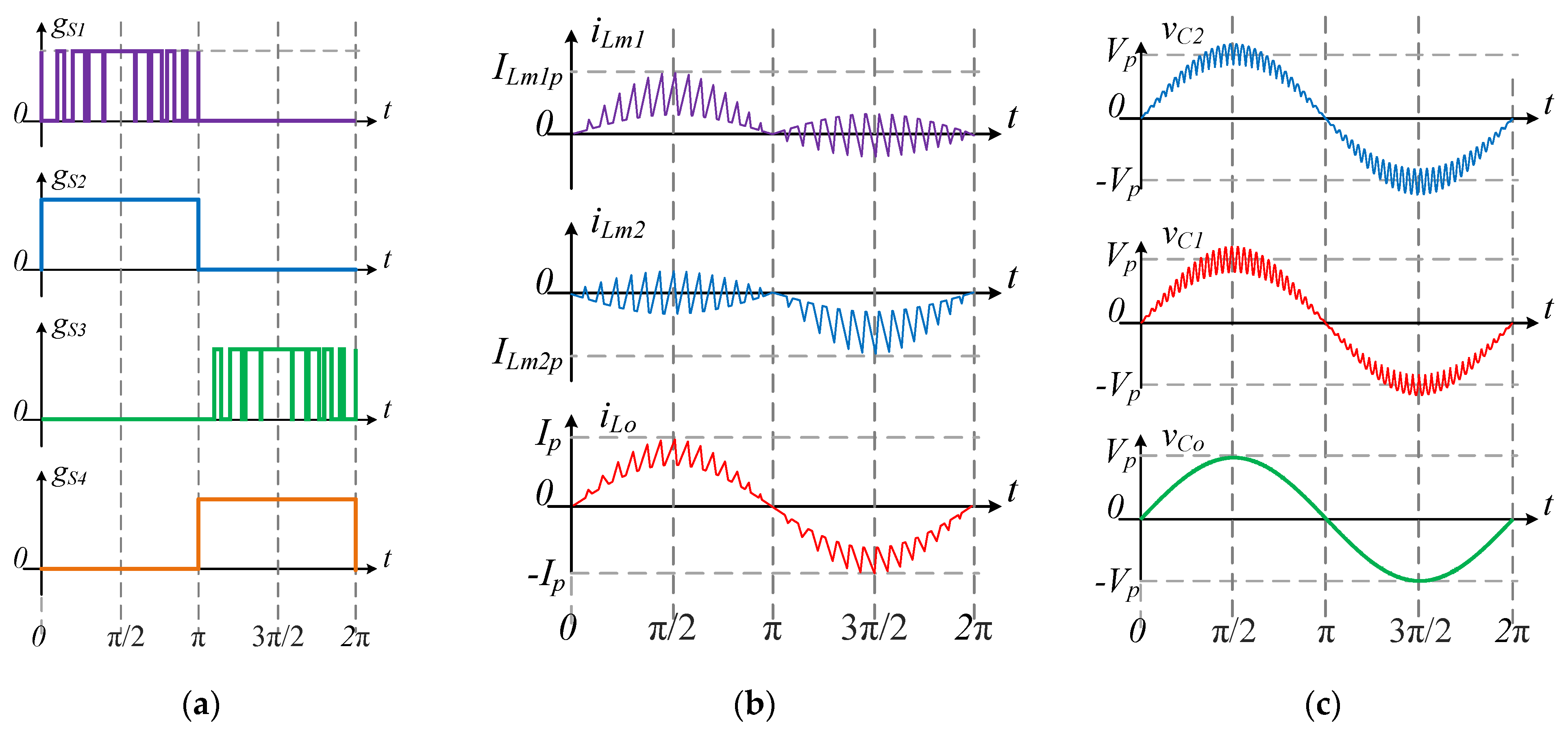
Figure 3a shows the commutation signals used in SP-IZI for the entire grid voltage period.
The voltage across the capacitor
presents the same value as the utility grid but with some voltage ripple. Similarly, the capacitor
also presents the same grid voltage waveform grid.
Figure 3c shows the voltage waveforms of the capacitors
and
and the utility grid voltage waveform.
Considering the equal voltage across the capacitors C1 and C2, the resulting inductors’ Lm1 and Lm2 voltages are the same. Thus, in each switching period, both inductors are magnetized and demagnetized with the same intensity, presenting the same current ripple.
On the other hand, during the whole positive half-wave cycle of the utility grid, the currents through the inductor
Lm2 and capacitor
C2 are the same, and the average capacitor current is null. Consequently, the average
Lm2 current also is null at this half-wave cycle. By symmetry of the topology, the average
Lm1 current is null at the negative half-wave cycle.
Figure 3b presents the current waveforms of the inductors for a complete utility grid period.
2.4. State-Space Model for the Inner Control Loop
Using the generalized switch-averaging modeling approach, the equations for the internal control loop in state-space is derived. The corresponding equations for the outer control loop are obtained, taking into account the power balance between the extracted PV array power and the injected power into the mains. Once the equations are obtained, the SP-IZI is analyzed for the operation in conjunction with the adopted MPPT and PLL algorithms.
During each switching period, the SP-IZI has three operating stages, , , and . Due to the symmetric operation of the proposed inverter, the same behavior for the positive half-wave cycle is equivalent to what occurs in the negative half-cycle. In this way, it is possible to simplify the converter structure for analysis such as the one acting in a half-cycle. It is noticed that, during a switching period, the current is divided between the inductors and , as compared to a conventional Zeta converter, where this current flows through the inductor , which is equivalent to a parallel association of and . Once both inductors present the same inductance, it is possible to write . The current is also divided between capacitors and , resulting in the coupling capacitor () for the conventional Zeta converter. The capacitor is assumed to be the parallel between and , and if , the equivalent capacitor is equivalent to .
The average state-space model is widely employed for modeling dynamic systems by its simplicity. The state-space model can be obtained for the static converters operating in both CCM and DCM [
43,
44,
45,
46,
47]. The SP-IZI presents the behavior as very close to the conventional Zeta converter operating in DCM. Thus, converter modeling is adopted as an equivalent model for the SP-IZI. The utility grid,
, can be represented as an input system in the matrix “
” in the state-space modeling. The voltage across the capacitor
also can be considered an input in this matrix. Furthermore, the line inductance (
Lg) and resistance (
rg) between the inverter and the utility are also taken into account. These considerations for converter modeling ensure a better system response. Thus,
Figure 4 presents the equivalent model used in the SP-IZI modeling.
In Ref. [
33], the state matrix of the converter operating in DCM was adequate through a modification in the matrix concerning the inductor current to represent the system behavior in discontinuous operation.
In addition, a generalized switch-averaging technique is adopted in [
31,
47], which is associated with the average state-space model to overcome the problems of representing the dynamical characteristics of the converter operating in DCM.
The employed modeling is based on the linearization of the state variables around the quiescent operating point, in which small oscillations are considered in the mean value. Hence, a generic variable
is represented by a mean term (DC) plus a first-order AC term,
, with X representing the DC term and
the AC term. There are considerations that the DC terms are much greater than the AC terms,
[
43].
The average state-space model is initially adopted for modeling the SP-IZI according to Equation (6).
where
is the state vector,
is the input vector,
is the average state matrix for a switching period,
is the average input matrix, and
M is the corrected matrix to DCM. The corrected matrix
can be obtained for the state-space averaging model of the SP-IZI operating in DCM as follows:
Performing the state-space averaging model and considering the adequacy matrix [see Equation (10)], the equivalent circuit representation for the SP-IZI presented in
Figure 4 is determined as follows:
where
;
;
;
; and
represents the output vector.
If the equivalent circuit operates in CCM, the adequacy matrix has a unit value associated with eliminating the operation step, which results in an averaging model also valid for the operation in CCM.
By manipulating (12) and (13), it is possible to determine the transfer function that relates the current in the inductor
to the duty cycle as follows:
where
and the matrices
and
are defined in order to obtain the closed-loop system matrices as follows:
where
,
, and
correspond to the respective state matrices for the passive elements during the operating stage
,
, and
;
,
, and
are the input matrices for the passive elements. The matrices
and
represent the output matrices of the generalized switch model, while
and
are the direct transition matrices of the generalized switch model. The matrix
is obtained by the operation stages averaging, i.e.,
. The same procedure step is also valid for obtaining the matrix
, i.e.,
.
2.5. Components Design
To guarantee the SP-IZI operates in DCM during all grid periods, the design of the components considers the voltage peak of the utility grid. However, the current injected into the grid presents a low ripple, and the output inductance is calculated as:
where
ILo is the average current during the voltage peak and
is the maximum ripple allowed.
The input inductors present a current ripple bigger than the average value and strongly influence the operation in the DCM. A maximum inductance can be obtained as follows:
The output capacitance is calculated following a similar procedure commonly used for a buck converter and depends on the current and voltage ripple allowed, as obtained by:
The coupling capacitances are designed in a range between two resonant frequencies,
ωrmin and
ωrmax. These capacitances are calculated as:
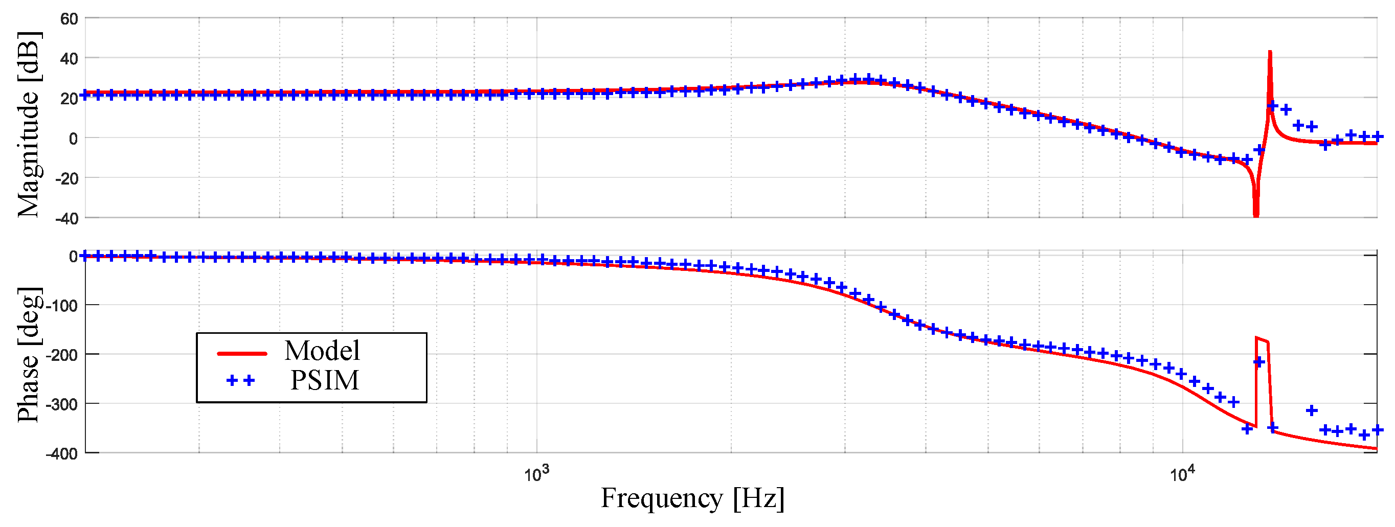
After the design of the components are combined, the modeling presented in (14) can obtain the frequency response, as shown in
Figure 5. There is a high similarity between the model and the circuit simulated in the software PSIM.
2.6. Modeling of the Outer Control Loop
The outer voltage control loop is modeled considering the energy conservation between the PV array and the utility grid. Ideally, the energy extracted from the PV array is the same as that injected into the grid. As the output of SP-IZI is sinusoidal, the active power can be determined through the voltage and current magnitude peaks,
Vp and
Ip, respectively. In this way, the power balance is defined as follows:
Replacing
for the ratio between the voltage across the capacitor
and the Laplace transform of the capacitor, applying small-signal perturbations, and posteriorly disregarding second-order terms as well as the oscillation in the grid, it is possible to find the transfer function that relates the PV array voltage to the grid current by (22).
2.7. MPPT and PLL Algorithm
As is well-known, the PV array presents non-linear characteristics curves (power versus voltage and current versus voltage). In addition, the PV array depends on the climate conditions, such as solar irradiance and temperature. Therefore, using algorithms to perform the maximum power point tracking (MPPT) is mandatory to extract the total available power at the PV array. Hence, this paper adopts the traditional Perturb and Observe (P and O) to reach the maximum available capacity of the PV array [
48,
49,
50,
51,
52].
A non-autonomous adaptative filter AF-αβ-pPLL technique is used in this paper for determining the synchronous unit vectors coordinates [sin(θ) and cos(θ)], which is detailed in [
53]. The AF is responsible for extracting the fundamental component of the grid voltage. The adopted AF-αβ-pPLL is designed to deal with voltage disturbances, such as voltage sags/swells, voltage harmonics, phase-angle jumps, and frequency variations [
53].
2.8. SP-IZI Control
The control of the SP-IZI is performed by a multiloop control as follows: (i) an inner current control loop controls the injected current into the grid (); (ii) an outer voltage control loop controls the PV array ); and (iii) a maximum power point tracking (MPPT) algorithm extracts the maximum power available at the PV array measuring the PV array voltage () and current (). Initially, the MPPT algorithm generates the reference voltage ) for the voltage control loop to extract the maximum PV array power. The voltage control loop’s proportional–integral (PI) controller computes the peak current reference () needed to maintain the PV array voltage regulated at the reference provided by the MPPT. Thus, such peak current reference () is used to generate the current control loop’s current reference (), which is synchronized to the grid voltage () using a phase-locked-loop (PLL) technique, i.e., the peak current is multiplied by the sinusoidal () vector. In addition, considering possible imbalance between the voltages over the input DC-bus capacitors ( and ) can occur, a DC current () is associated with the sinusoidal current reference () to guarantee a balanced voltage between and . Finally, the current control loop’s PI controller generates the duty cycle used in the switching logic to control the switching devices.
The proportional and integral gains of the PI controllers are tuned based on the procedure design proposed in [
54]. The block diagram of the control diagram is presented in
Figure 6a, while the block diagram of the signal logic adopted to control the switches of the SP-IZI is depicted in
Figure 6b.
3. Comparison between the SP-IZI and the MZI
The proposed SP-IZI operates similarly to the integrated inverters called MZIs [
39,
40]. In addition, accordingly to the characteristics presented by the SP-IZI, the following advantages are obtained when compared to the MZI: (i) the static converter gain in DCM is identical to the traditional DC-DC Zeta converter; (ii) it presents reduced voltage stress over the switches and diodes; and (iii) it can operate in an off-grid mode for a different type of load.
The MZI is based on the modified Zeta converter and controlled to inject a sinusoidal current into the utility grid. The topology operates in DCM. Therefore, a switching period is divided into three operation stages referred to as
ta,
tb, and
tc.
Figure 7 presents the MZI.
The diodes Di1 and Di2 in series with the inductors Li1 and Li2 prevent negative current during the third operation stage through the inductors mentioned. These diodes also prevent the current through all passive elements during the first and second stages, as in the SP-IZI.
According to the electrical circuit of the MZI and its operation, besides considering the peak amplitude of the grid, the gain of the inverter is determined as:
where
Da and
Db represent the respective first and second operation stages during the peak voltage of the grid,
fs is the switching frequency,
Li is the input inductance,
Vp is the peak voltage of the grid, and
Po is the output power.
The voltage across the capacitors
Ci1 and
Ci2 are distinct between the MZI and the SP-IZI or the conventional Zeta converter. In the MZI, these voltages are related to the first operation stage. In the SP-IZI, the voltage of the intermediate capacitor is similar to that of the utility grid. The voltage across the intermediate capacitors to the MZI is determined as:
According to (23), the first and second operation stages depend on the input inductance, switching frequency, grid voltage, and output power. Maintaining the output power and switching frequency as constant, in addition to considering the peak voltage of the utility grid, the voltages across the coupling capacitors (24) are related to the input inductance, in which lower values result in higher voltages. Conversely, high inductance values make the topology operate in CCM.
Figure 8a presents the intermediate capacitors’ average voltage dependence with the input inductance to the MZI and the voltage across the coupling capacitors to the SP-IZI.
Consequently, the maximum voltages across the switches
Si1 and
Si2 in the proposed inverter, MZI, depend on the input inductance and the voltage across the coupling capacitors. Thus, the voltages across these switches are described as
.
Figure 8b shows the maximum voltage across the switches
Si2 and
Si2 to the MZI and the
S1 and
S3 to the SP-IZI.
In brief, the voltages across the semiconductors are higher in the MZI than in the SP-IZI, which causes limitations in the operation range and power losses during commutation.
Table 1 compares the main parameters of the MZI and the SP-IZI.
Based on the equations and the operational description of the SP-IZI using the MPP power in standard test conditions (STC), the theoretical values from the RMS currents through the semiconductors and inductors are calculated. In addition, the maximum semiconductors’ and intermediate capacitors’ voltages are determined. The MZI is also evaluated for the same conditions.
Table 2 shows the main parameters of the adopted PV module. The theoretical and practical implementation have assumed eight series-connected PV array panels achieving a maximum nominal power of 432 Wp. Therefore,
Table 3 compares the theoretical RMS values of the MZI and SP-IZI.
The SP-IZI presents current through all passive elements. Therefore, the semiconductors’ currents are the sum of the inductors’ currents, resulting in not much higher RMS values when compared to the MZI. Thus, these currents can cause conduction losses in the semiconductors. On the other hand, the currents through the inductors present lower values in SP-IZI.
4. Experimental Results
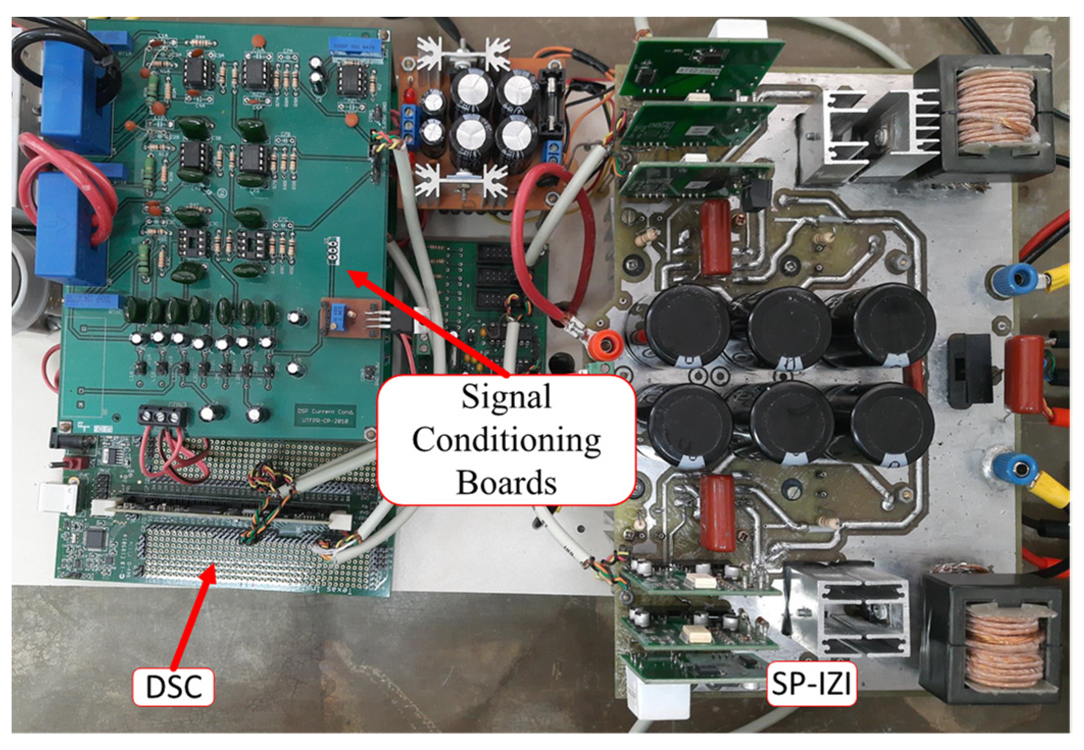
An experimental prototype was developed to evaluate the SP-IZI, as depicted in
Figure 9. The experimental setup employs the discrete IGBT IRGP4650D (Infineon, Neubiberg, Germany) and 30ETH06 diodes (International Rectifier, El Segundo, CA, USA). The characteristics curves of the PV array were performed using a bidirectional PV array emulator IT6012C-800-50 (Itech, New Taipei City, Taiwan) in conjunction with the software SAS100L (Itech). The entire system was controlled using a digital signal controller (DSC), a TMS320F28335 (Texas Instruments, Dallas, TX, USA), in which the current and voltage quantities were measured by means of signal-conditioning boards that employ Hall-effect transducers (LEM, Geneva, Switzerland). The system’s algorithms were embedded in the DSC. The experimental results were obtained by digital oscilloscope, the TPS2024 (Tektronix, Beaverton, OR, USA), while the power factor (PF) and total harmonic distortion were measured using the Power Quality Analyzer 43B (Fluke, Everett, WA, USA).
Table 4 presents the main parameters employed in the experimental tests of the SP-IZI.
Firstly, the SP-IZI was evaluated for three different levels of solar irradiance employing the PV emulator, in which the PV array voltage was equal to 140 V. Hence, the peak amplitude of the inverter currents injected into the grid is described as follows: (i) Scenario 1: 2 A; (ii) Scenario 2: 3 A; and (iii) Scenario 3: 4.8 A.
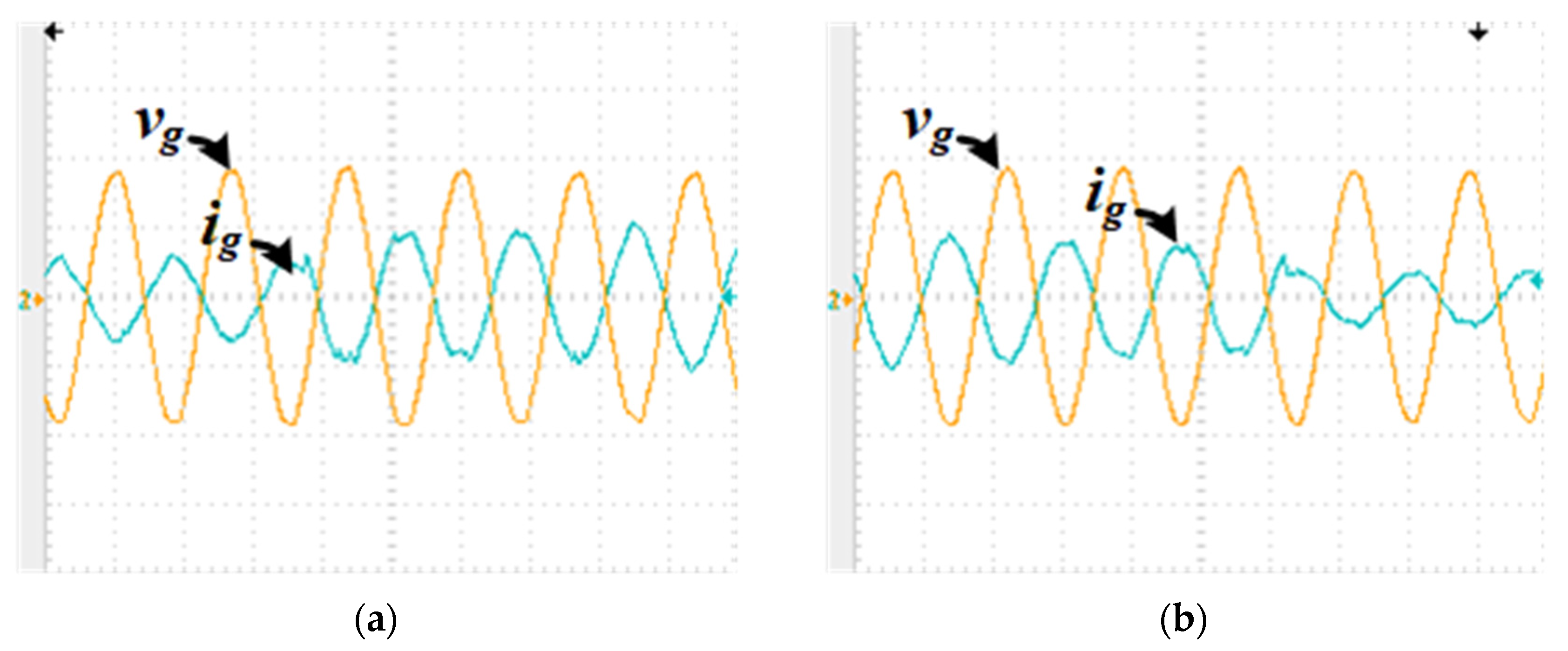
Figure 10 shows the grid voltage and the current injected into the grid for the three evaluated scenarios. As noted, the grid-injected currents present sinusoidal waveforms in opposite-phase to the grid voltage for all the considered scenarios.
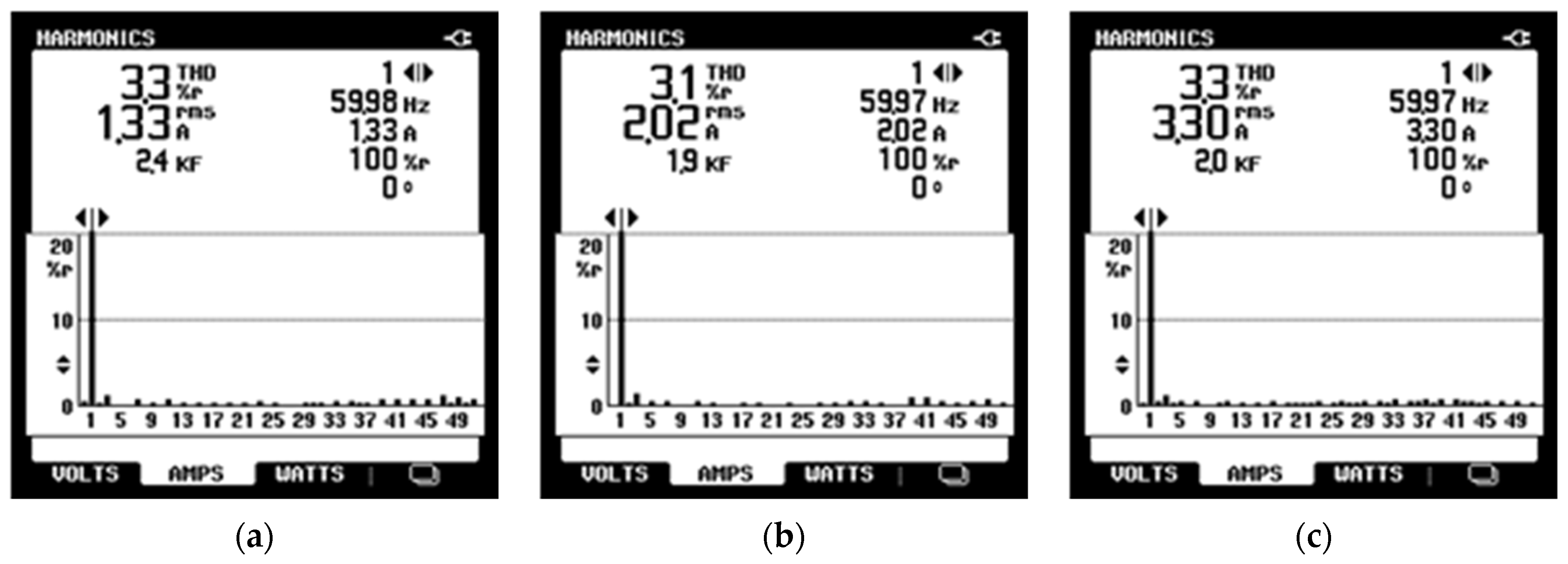
Figure 11 shows the total harmonic distortion (THD) for the three inverter currents shown in
Figure 10. It can be observed that the SP-IZI currents are sinusoidal, meeting the requirements of the standards [
41,
42], i.e., the injected currents presented a maximum THD of around 3.3%, validating the feasibility and theoretical development of the proposed inverter.
Figure 12 presents the dynamic performance of the SP-IZI considering changes in solar irradiance. The changes are performed from half of the power rate to nominal PV array power rate and vice versa (50% to 100% and 100% to 50%). As can be observed, the proposed SP-IZI acts very fast when abrupt solar irradiance changes occur.
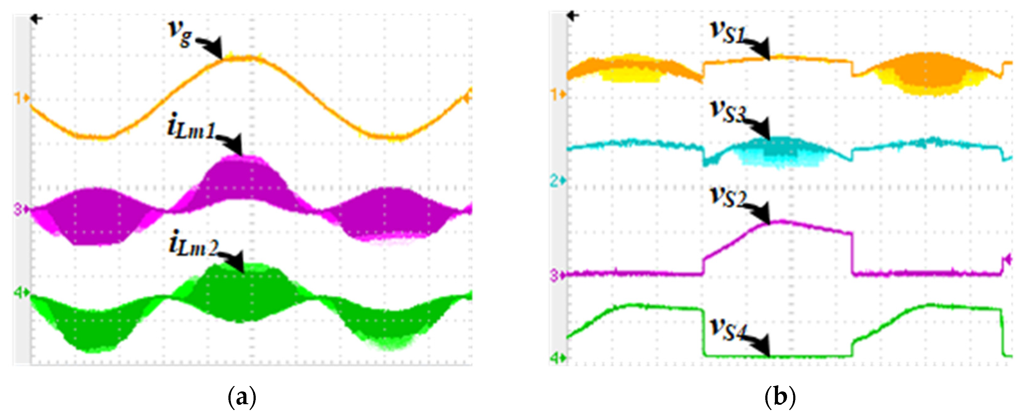
The currents through the inductors
and
are presented in
Figure 13a, while the voltages across the switches
,
,
, and
are presented in
Figure 13b. It can be noted that the experimental results presented in
Figure 12 can be compared and evaluated to the theoretical development shown in
Figure 3. These results demonstrated that the proposed SP-IZI operates following the developed mathematical equations and that the inverter is feasible and reliable.
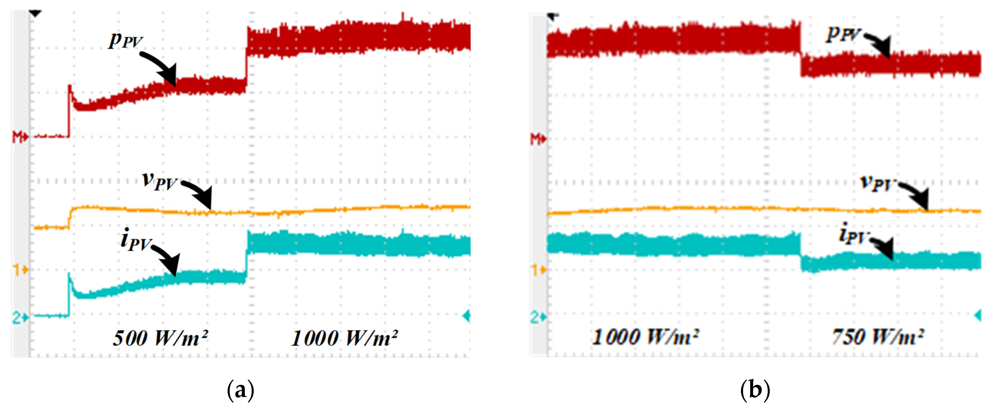
In STC, the performance of the P and O MPPT algorithm was evaluated considering the solar irradiance change from 500 W/m
2 to 1000 W/m
2 and from 1000 W/m
2 to 750 W/m
2, as shown in
Figure 14. As observed, the P and O MPPT technique used in the SP-IZI can reach the maximum power point and acts very fast during abrupt solar irradiance changes. In addition,
Figure 14 shows that the PV array voltage is below 160 V in all cases, while the grid peak voltage is near 200 V [see
Figure 13a]. This demonstrates that the proposed SP-IZI can boost the input voltage and, simultaneously, injects in the grid a sinusoidal and regulated current into the utility with low harmonic distortion, as discussed above. Hence, all such results demonstrate that the proposed converter is useful and suitable for PV applications.
5. Conclusions
This paper presented the implementation of an integrated inverter topology based on Zeta converters named SP-IZI. The proposed inverter increased the input voltage (PV array voltage) and injected a sinusoidal current into the grid with low total harmonic distortion.
The SP-IZI presented advantages compared to the MZI when both inverters were operating in DCM. The voltages across the semiconductors and coupling capacitors are lower and do not depend on the input inductance or the operation stages. The operation of the SP-IZI is similar to the conventional DC-DC Zeta converter, in which the third stage is well-defined. The SP-IZI presents the following advantages compared to the MZI: (i) the voltage in coupling capacitors is 13% lower; (ii) voltage stresses in switches and diodes are 40% lower; and (iii) static gain is similar to the traditional Zeta converter.
From the employed modeling technique, the SP-IZI transfer functions for the inner and outer control loops were derived. In addition, by the analysis of frequency response, it was possible to obtain the proportional and integral gains of the PI controllers.
Through experimental results, the effectiveness and feasibility of an SP-IZI were evaluated and demonstrated. In addition, simulation and experimental results corroborated the theoretical development.
As could be observed from the achieved results, the proposed SP-IZI can replace—with advantages—the traditional PV system constructed by the cascade association of a step-up DC-DC converter and a voltage source inverter.


