Article

Research on Near-Field Propagation Characteristics of Partial Discharge Electromagnetic Wave Signal in Switchgear

1
College of Science, Kunming University of Science and Technology, Kunming 650504, China
2
Faculty of Civil Engineering and Architecture, Kunming University of Science and Technology, Kunming 650504, China
3
College of Mechanical and Electrical Engineering, Kunming University of Science and Technology, Kunming 650504, China
*
Author to whom correspondence should be addressed.
Energies 2023, 16(8), 3372; https://doi.org/10.3390/en16083372
Submission received: 27 February 2023 / Revised: 26 March 2023 / Accepted: 28 March 2023 / Published: 12 April 2023

Abstract

:
In the authors’ previous research, a new method for partial discharge detection in the switchgear based on near-field detection was proposed. The content of this paper is the continuation of the authors’ previous research. In order to realize the reasonable layout of the near-field magnetic field probe for partial discharge detection in the switchgear, this paper simulates and analyzes the influence of the internal structure of the switchgear on the near-field propagation characteristics of the electromagnetic wave signal generated by partial discharge, and determines the installation position of the near-field probe in the switchgear. Firstly, the propagation characteristics of electromagnetic wave signals in the different media of the switchgear are analyzed, and the switchgear model is established. Then, based on the finite difference time domain method, the influence of different devices in the switchgear on the near-field propagation of the partial discharge electromagnetic wave signal is simulated. The simulation results show that the current transformer, insulator, busbar and cabinet all obviously attenuate the amplitude of the near-field electromagnetic wave signals generated by partial discharge, and the insulator causes obvious signal distortion. Finally, it is determined that the near-field probe can be installed on the inner wall or the right wall near the bottom plate of the switchgear.

1. Introduction

The switchgear is an important piece of electrical equipment in the power system. Once it fails, causes serious accidents, such as tripping and power failure [1,2], which will have a huge impact on the security of the power grid [3]. According to statistics [4,5,6], insulation faults account for more than 30% of the total faults of high-voltage switchgears. Insulation failure is usually accompanied by partial discharge (PD), which can be used as an important basis for judging the insulation status of electrical equipment [7]. Therefore, the detection of PD in the switchgear can timely find the hidden trouble, prevent accidents and reduce economic losses.
In the authors’ previous research [8], a new method for switchgear partial discharge detection based on the near-field detection principle was proposed. The content of this paper is the continuation of this previous research; as such, it is the first time that the near-field propagation characteristics of the electromagnetic wave signals generated by partial discharge in the switchgear have been studied. This is helpful in order to determine the best installation position of the near-field probe in the switchgear and is of great significance in terms of improving its detection accuracy using the near-field detection method.
At present, research on the propagation characteristics of the electromagnetic wave signals generated by partial discharge in electrical equipment mainly focuses on the gas-insulated switchgear (GIS) and transformer. Wu Yunjie [9] and other scholars studied the propagation characteristics of ultra-high frequency (UHF, 300 MHz–3 GHz) signals generated by partial discharge in the typical structure of 252 kV GIS; this was achieved by conducting experiments that provided theoretical guidance for the layout of built-in sensors detecting partial discharge in GIS. Ahmad Drawish [10] and other scholars used time domain simulation to study the influence of different barriers on the propagation of UHF electromagnetic wave signals generated by partial discharge. Zhao Tao and other scholars [11] studied the influence of insulation gasket, L-shaped and T-shaped structures on the propagation of UHF electromagnetic signals generated by partial discharge in the GIS system. According to the research results, the location of UHF sensors can be appropriately selected, so as to reduce the attenuation effect introduced by L-shaped and T-shaped structures. Zhao Xiaoxing [12] and other scholars studied the propagation characteristics of UHF partial discharge signals in transformer gaps, and provided suggestions for the installation position of sensors in the actual system for detecting UHF partial discharge signals in transformer gaps. Du Jinchao [13] and other scholars studied the propagation characteristics of partial discharge UHF signals in real transformers. Reza Rostaminia [14] and other scholars studied the influence of transformer core on the propagation of UHF electromagnetic wave signals generated by partial discharge.
However, GIS is a coaxial waveguide structure, and the iron core and winding play a major role in the electromagnetic wave propagation inside the transformer, which is completely inconsistent with the actual situation inside the switchgear, so the above laws are not completely applicable to the switchgear. In addition, at present, there are few studies on the propagation characteristics of electromagnetic waves in switchgears, and all of them focus on the propagation characteristics of UHF (300 MHz–3 GHz) band electromagnetic wave signals [15,16,17] in the far field. However, although many substations have established perfect condition monitoring systems based on UHF detection technology, insulation faults continue to occur [18,19]. This is because [20,21] there may be some sub-millimeter cracks in insulators, and the discharge caused by them is mainly glow discharge, and the frequency of discharge is basically below 150 MHz, which cannot reach the UHF band. In addition, as a common type of partial discharge, the signal of tip discharge is mainly distributed below 200 MHz [22,23]. Therefore, the energy of partial discharge signals is mainly concentrated below 200 MHz [24], and the placement positions of partial discharge sensors in the switchgear are mostly in the near-field area of these signals.
Therefore, it is of great significance to study the propagation characteristics of energy-concentrated frequency band signals in switchgears in the near-field area, which is expected to determine the best installation position of near-field probes; this is conducive to the quantitative and pattern recognition of partial discharge signals and the determination of targeted maintenance schemes, and can also provide an important basis for correctly evaluating the harm of PD and formulating reasonable disposal measures.
In this paper, firstly, the propagation characteristics of electromagnetic wave signals generated by partial discharge in the switchgear in different media are analyzed, and then the switchgear model is established. Based on the finite difference time domain method, a series of simulation studies on the near-field propagation characteristics of electromagnetic wave signals generated by different components of the switchgear, such as current transformers, insulators, buses and cabinets, are carried out in XFDTD software. Finally, based on the above simulation results, the installable position of the near-field probe in the switchgear is analyzed.

2. Propagation Analysis of PD Electromagnetic Wave Signal

The actual environment of the PD electromagnetic wave signal in the switchgear during its propagation always involves various media. In general, the process of electromagnetic wave signal propagation can also be regarded as the physical process of electromagnetic wave and medium interaction. Under the action of electromagnetic wave, various electromagnetic effects such as polarization, magnetization and conduction will be produced in the medium, which, in turn, will exert various influences on the electromagnetic wave in propagation. Therefore, the propagation characteristics of electromagnetic waves are not only related to the characteristic parameters of the medium, including dielectric constant ε , permeability μ , and conductivity σ , but are also related to the characteristic parameters of the electromagnetic wave itself, frequency and polarization. The latter can make the same medium show different characteristics and boundary conditions. Generally speaking, in various characteristic media, the propagation mechanism of the electromagnetic wave involves a series of physical processes such as absorption, refraction, reflection, scattering, diffraction, guidance and resonance, multipath interference and the Doppler shift effect. That is, the signal may suffer from attenuation, fading, polarization shift, time-domain and frequency-domain distortion, and other effects, thus having complex spatio-temporal characteristics.
Therefore, if we want to research the propagation characteristics of PD electromagnetic wave signals in the switchgear, we must analyze their propagation characteristics in different media. Combined with the material characteristics of components in the switchgear, this paper mainly analyzes the propagation characteristics of electromagnetic wave signals in the insulating medium, conductive medium and interface.

2.1. Propagation Characteristics of Electromagnetic Wave Signal in Insulating Medium

The insulating medium is a material that does not easily conduct electricity, and whose resistivity is very high. Insulators that are used to support and fix current-carrying conductors can be seen everywhere in the switchgear. The material is generally epoxy resin, which is a common insulating medium. When the electromagnetic wave propagates in the insulating medium, its propagation speed v and instantaneous electromagnetic energy flow density vector S are, respectively:
v = 1 μ ε
S = e n 1 η E 2 = e n η H 2
where μ , ε and η are the permeability, dielectric constant and intrinsic impedance of the medium, respectively, and e n is the unit vector of the propagation direction of the electromagnetic wave. The permeability, dielectric constant and intrinsic impedance of the insulating medium are all real numbers. It can be seen from the above that when the electromagnetic wave propagates in the insulating medium, its propagation speed is mainly affected by the characteristics of the medium itself. In addition, the propagation direction of electromagnetic energy is consistent with that of the electromagnetic wave. The amplitude of the energy density of the electromagnetic field remains unchanged during the propagation process, that is, the propagation of the electromagnetic wave signal in the insulating medium is almost not attenuated.

2.2. Propagation Characteristics of Electromagnetic Wave Signal in Conductive Medium

The conductive medium is a medium with free charge, and its conductivity σ is not 0. When the electromagnetic wave propagates in the conductive medium, due to the existence of free charge, under the effect of the electric field of the electromagnetic wave, the free charge will make a macroscopic directional movement to form a conduction current, and the conduction current will generate joule heat, which is consumed on the resistance of the conductive medium, thus causing the loss of electromagnetic wave energy. Therefore, the electromagnetic wave inside the conductor will attenuate when it propagates, and its electromagnetic energy will be converted into heat.
In general, the propagation constant γ in conductive media is a complex number, which can be expressed as follows:
γ = j k c = j ω μ ε c = α + j β
where k c is the wave number in the conductive medium; ω is the angular frequency of the electromagnetic wave; μ is the permeability of the medium; α is the attenuation constant, which represents the attenuation of the amplitude of the electromagnetic wave for each unit distance, in Np/m; β is the phase constant, representing the change in the phase in unit distance, in rad/m; and ε c is the complex permittivity of the conductive medium, whose basic expression is as follows:
γ = j ω μ ε 1 j σ ω ε
Generally speaking, conductive media can be divided into three types according to the size of σ ω ε :
(1) Weak conductive medium, that is, a conductive medium that meets the condition Formula (5). In this medium, the displacement current plays a major role, while the influence of the conduction current is negligible. The loss caused by the conduction current is very small. Its attenuation constant α and phase constant β can be approximately expressed as Formulas (6) and (7), that is, in a weakly conductive medium, the attenuation constant of the electromagnetic wave increases with the increase in the permeability and conductivity of the medium.
σ ω ε 1
α σ 2 μ ε
β = ω μ ε
(2) A good conductor is a conductive medium that meets the condition Formula (8). In this medium, the conduction current plays a major role, while the influence of the displacement current is negligible. The attenuation constant a and phase constant b can be approximately expressed as Formula (9). According to Formula (9), in a good conductor, the attenuation constant of the electromagnetic wave increases with the increase in the wave frequency, the permeability and conductivity of the medium.
σ ω ε 1
α β π f μ σ
(3) The influence of the conduction current and displacement current cannot be ignored for the ordinary conductive medium, which is the medium meets neither of the above two conditions. The attenuation constant α and phase constant β of the electromagnetic wave in the medium can be expressed as Formulas (10) and (11), respectively. That is, when the electromagnetic wave propagates in the general conductive medium, its attenuation constant is between the weak conductive medium and the good conductor.
α = ω μ ε 2 1 + σ ω ε 2 1
β = ω μ ε 2 1 + σ ω ε 2 + 1

2.3. Propagation Characteristics of Electromagnetic Wave Signal at the Interface of Composite Media

When the electromagnetic wave propagates at the interface of the composite medium, due to the characteristics of the medium itself, that is, because the wave impedance η is different, the electromagnetic wave will be refracted and reflected at the interface. Considering that the expression of wave impedance is Formula (12), if the ratio of permeability and the dielectric constant of two media is the same, when the electromagnetic wave propagates to the interface, it will directly spread to the other media, without reflection; if the ratio of the permeability and permittivity of the two media is different, the electromagnetic wave will be refracted and reflected at the composite interface.
η = μ ε

3. Simulation Scheme Design

3.1. Basic Principle of Finite-Difference Time-Domain Method

The finite-difference time-domain method (FDTD) is a numerical method suitable for solving broadband transient electromagnetic field problems in complex environments. It was first proposed by Yee in 1966 [25].
The starting point of the FDTD method is Maxwell’s rotation equation, which can reflect the essence of the electromagnetic field. Combined with the constitutive relation of the medium, the Maxwell rotation equation is expanded in the rectangular coordinate system to obtain six coupled partial differential equations, and then the intermediate difference is used to replace the partial differential of the time and space coordinates, respectively, to obtain the following six difference equations:
H x n + 1 2 i , j + 1 2 , k + 1 2 = 1 ρ i , j + 1 2 , k + 1 2 Δ t 2 μ i , j + 1 2 , k + 1 2 1 + ρ i , j + 1 2 , k + 1 2 Δ t 2 μ i , j + 1 2 , k + 1 2 H x n 1 2 i , j + 1 2 , k + 1 2 + Δ t μ i , j + 1 2 , k + 1 2 1 1 + ρ i , j + 1 2 , k + 1 2 Δ t / 2 μ i , j + 1 2 , k + 1 2 × E y n i , j + 1 2 , k + 1 E y n i , j + 1 2 , k Δ z + E z n i , j , k + 1 2 E z n i , j + 1 , k + 1 2 Δ y
H y n + 1 2 i + 1 2 , j , k + 1 2 = 1 ρ i + 1 2 , j , k + 1 2 Δ t 2 μ i + 1 2 , j , k + 1 2 1 + ρ i + 1 2 , j , k + 1 2 Δ t 2 μ i + 1 2 , j , k + 1 2 H y n 1 2 i + 1 2 , j , k + 1 2 + Δ t μ i + 1 2 , j , k + 1 2 1 1 + ρ i + 1 2 , j , k + 1 2 Δ t / 2 μ i + 1 2 , j , k + 1 2 × E z n i + 1 , j , k + 1 2 E z n i , j , k + 1 2 Δ x + E x n i + 1 2 , j , k E x n i + 1 2 , j , k + 1 Δ z
H z n + 1 2 i + 1 2 , j + 1 2 , k = 1 ρ i + 1 2 , j + 1 2 , k Δ t 2 μ i + 1 2 , j + 1 2 , k 1 + ρ i + 1 2 , j + 1 2 , k Δ t 2 μ i + 1 2 , j + 1 2 , k H z n 1 2 i + 1 2 , j + 1 2 , k + Δ t μ i + 1 2 , j + 1 2 , k 1 1 + ρ i + 1 2 , j + 1 2 , k Δ t / 2 μ i + 1 2 , j + 1 2 , k × E x n i + 1 2 , j + 1 , k E x n i + 1 2 , j , k Δ y + E y n i , j + 1 2 , k E y n i + 1 , j + 1 2 , k Δ x
E x n + 1 i + 1 2 , j , k = 1 σ i + 1 2 , j , k Δ t 2 ε i + 1 2 , j , k 1 + σ i + 1 2 , j , k Δ t 2 ε i + 1 2 , j , k E x n i + 1 2 , j , k + Δ t ε i + 1 2 , j , k 1 1 + σ i + 1 2 , j , k Δ t / 2 ε i + 1 2 , j , k × H z n + 1 2 i + 1 2 , j + 1 2 , k H z n + 1 2 i + 1 2 , j 1 2 , k Δ y + H y n + 1 2 i + 1 2 , j , k 1 2 H y n + 1 2 i + 1 2 , j , k + 1 2 Δ z
E y n + 1 i , j + 1 2 , k = 1 σ i , j + 1 2 , k Δ t 2 ε i , j + 1 2 , k 1 + σ i , j + 1 2 , k Δ t 2 ε i , j + 1 2 , k E y n i , j + 1 2 , k + Δ t ε i , j + 1 2 , k 1 1 + σ i , j + 1 2 , k Δ t / 2 ε i , j + 1 2 , k × H x n + 1 2 i , j + 1 2 , k + 1 2 H x n + 1 2 i , j + 1 2 , k 1 2 Δ z + H z n + 1 2 i 1 2 , j + 1 2 , k H z n + 1 2 i + 1 2 , j + 1 2 , k Δ x
E z n + 1 i , j , k + 1 2 = 1 σ i , j , k + 1 2 Δ t 2 ε i , j , k + 1 2 1 + σ i , j , k + 1 2 Δ t 2 ε i , j , k + 1 2 E z n i , j , k + 1 2 + Δ t ε i , j , k + 1 2 1 1 + σ i , j , k + 1 2 Δ t / 2 ε i , j , k + 1 2 × H y n + 1 2 i + 1 2 , j , k + 1 2 H y n + 1 2 i 1 2 , j , k + 1 2 Δ x + H x n + 1 2 i , j 1 2 , k + 1 2 H x n + 1 2 i , j + 1 2 , k + 1 2 Δ y
According to Formulas (13)~(18), the new value of each field component at each grid point depends on the value of the point at the previous time step and the value of the field component of another field quantity at the adjacent point around the point at half a time step. That is, the electric field component of time 3 can be derived from the electric field component of time 1 and the magnetic field component of time 2, and then the magnetic field component of time 4 can be derived from the magnetic field component of time 2 and the electric field component of time 3, and so on, and the iteration cycle is repeated until any specified time.

3.2. Establishment of Switchgear Model

The PD researched in this paper is based on a KYN28A-12 indoor armored removable AC metal-enclosed switchgear. The switchgear is mainly used for the power generation, transmission, distribution, energy conversion and consumption of the power system, and plays the role of on-off, control or protection. It meets the requirements of GB3906-91, GB11022-99, DL404-91, IEC-298 (1990) and other standards. According to the analysis in Section 2, when establishing the model, the influence of the switchgear cabinet and internal components, including the busbar, current transformer (CT) and insulator, on the propagation characteristics of the partial discharge electromagnetic wave signal is mainly considered. The material parameters of the above parts are shown in Table 1.
Because the switchgear model is complex and has many components, the switchgear model containing the above components can be built based on the real size of SOLIDWORKS software based on the 3D CAD system, and the results are shown in Figure 1.

3.3. Simulation Parameter Setting

The setting of the simulation parameters of the software generally includes three steps: constructing geometry, defining and creating mesh, and defining operation parameters.
Geometric construction generally includes model construction and material allocation. The steps for this are as follows: Import the model in the CAD file format established in the previous section into XFDTD software. Then, according to the material parameters of each component in Table 1, assign materials to each component by creating the Materials definition object in the project tree.
Meshing is an important step in XFDTD software simulation. If the spatial step of mesh generation is too large, it will bring about large numerical dispersion, that is, the phase velocity of the electromagnetic wave will change with the wavelength, propagation direction and variable discretization [26], which will lead to the destruction of the pulse waveform in the simulation process, artificial anisotropy and false refraction. This effect can be infinitely reduced by reducing the space and time steps taken in the discretization process. Generally speaking, to make the numerical dispersion meet the requirements, the size of the maximum cell grid can be determined by the following formula:
L = c 10 f m a x
where c is the speed of light, 3 × 10 8   m / s in free space, and f is the highest frequency of excitation. Because the frequency band analyzed in this paper is below the UHF frequency band, the maximum frequency excited in the simulation is 300 MHz. According to Formula (19), the size of the largest cell grid should be set to 100 mm.
The last step of the simulation parameters is to set the operation parameters, including the external boundary settings and the excitation settings.
The boundary conditions of the environment are generally set as a seven-layer PML absorption boundary.
At present, in many simulations of the propagation characteristics of PD electromagnetic wave signals, the Gaussian pulse source in the form of pulse function is generally used as the source to simulate the Gaussian pulse source [27]. Its time-domain waveform and frequency-domain waveform are shown in Figure 2 and Figure 3, respectively.
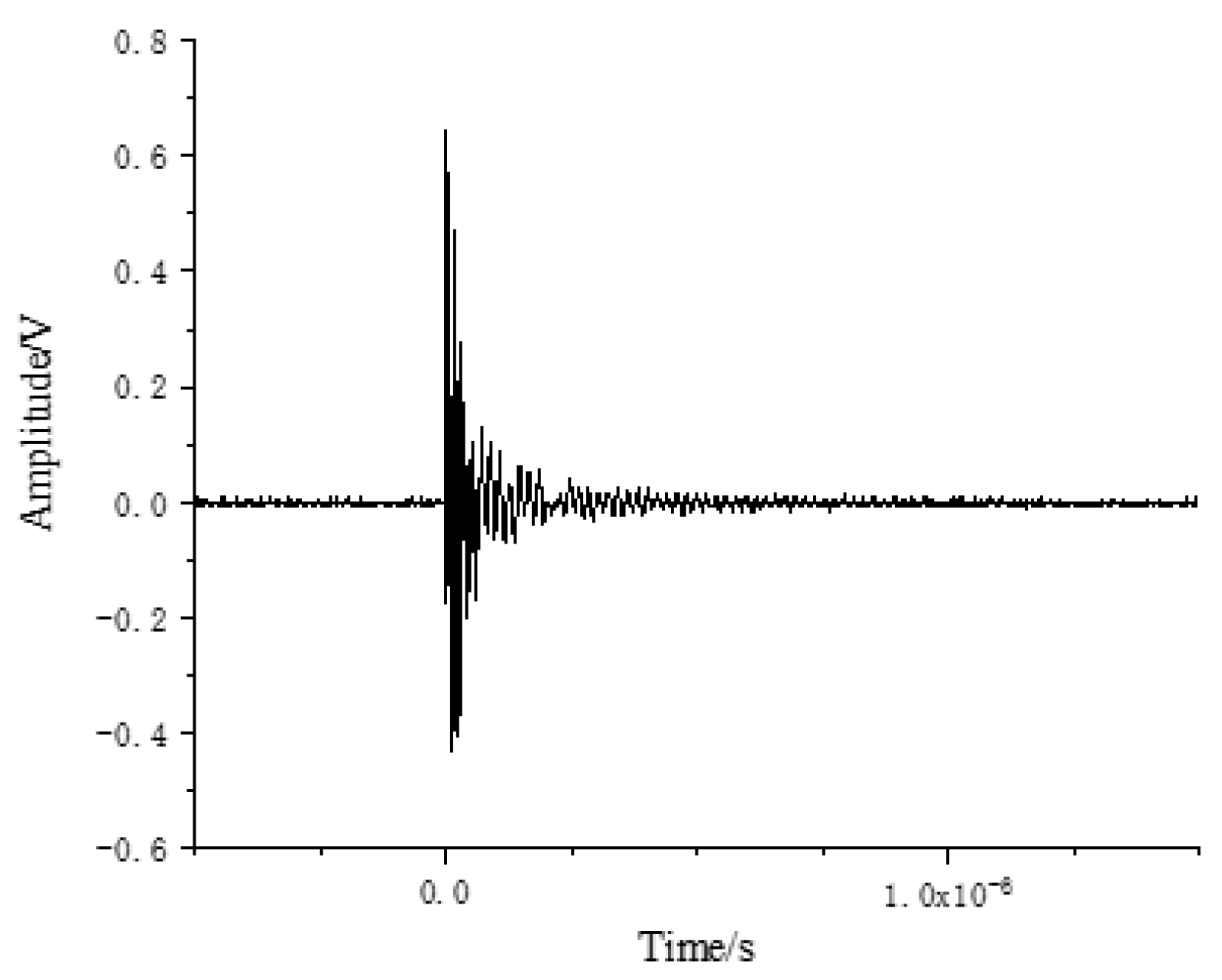
However, the actual PD electromagnetic wave signal is quite different from the ideal Gaussian pulse. Since XFDTD itself has the function of user-defined waveform, the signal data text can be directly imported into the software. Therefore, this paper directly uses the PD electromagnetic wave signal received by the near-field probe designed in the previous research [7] as the excitation source waveform, and its time-domain waveform is shown in Figure 4.

4. Analysis of Simulation Results

4.1. Influence of Current Transformer on Near-Field Propagation Characteristics of PD Electromagnetic Wave

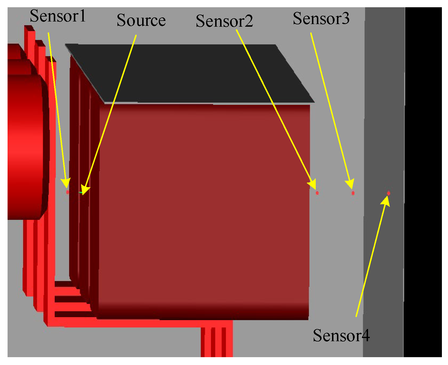
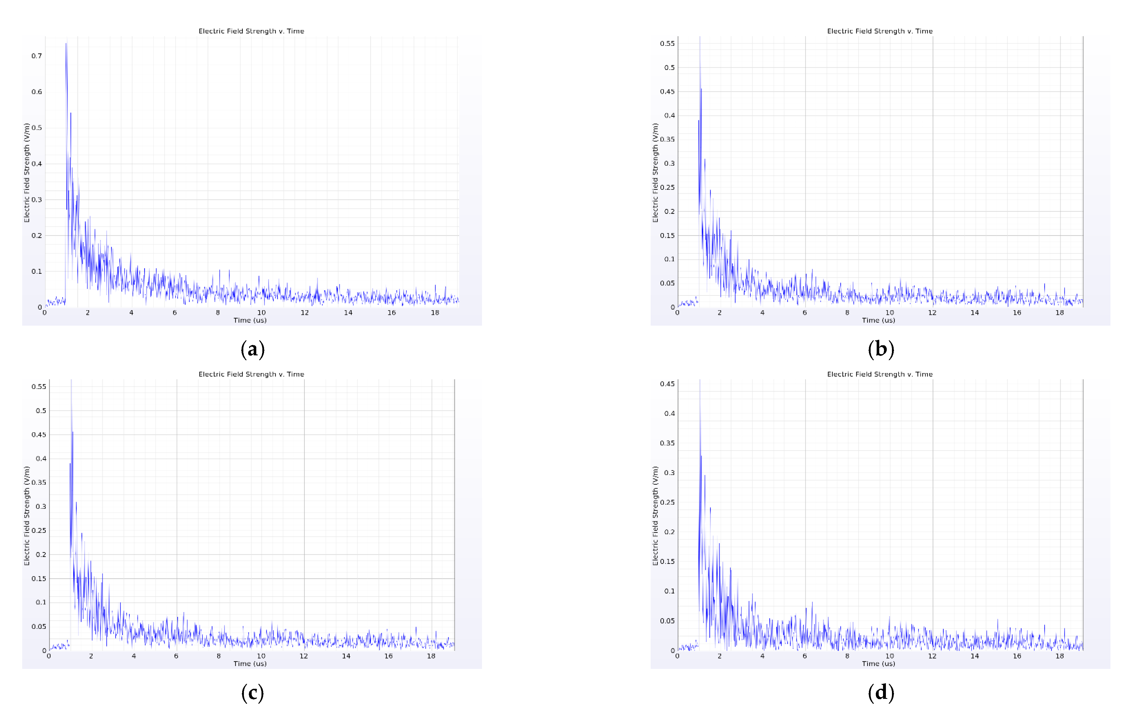
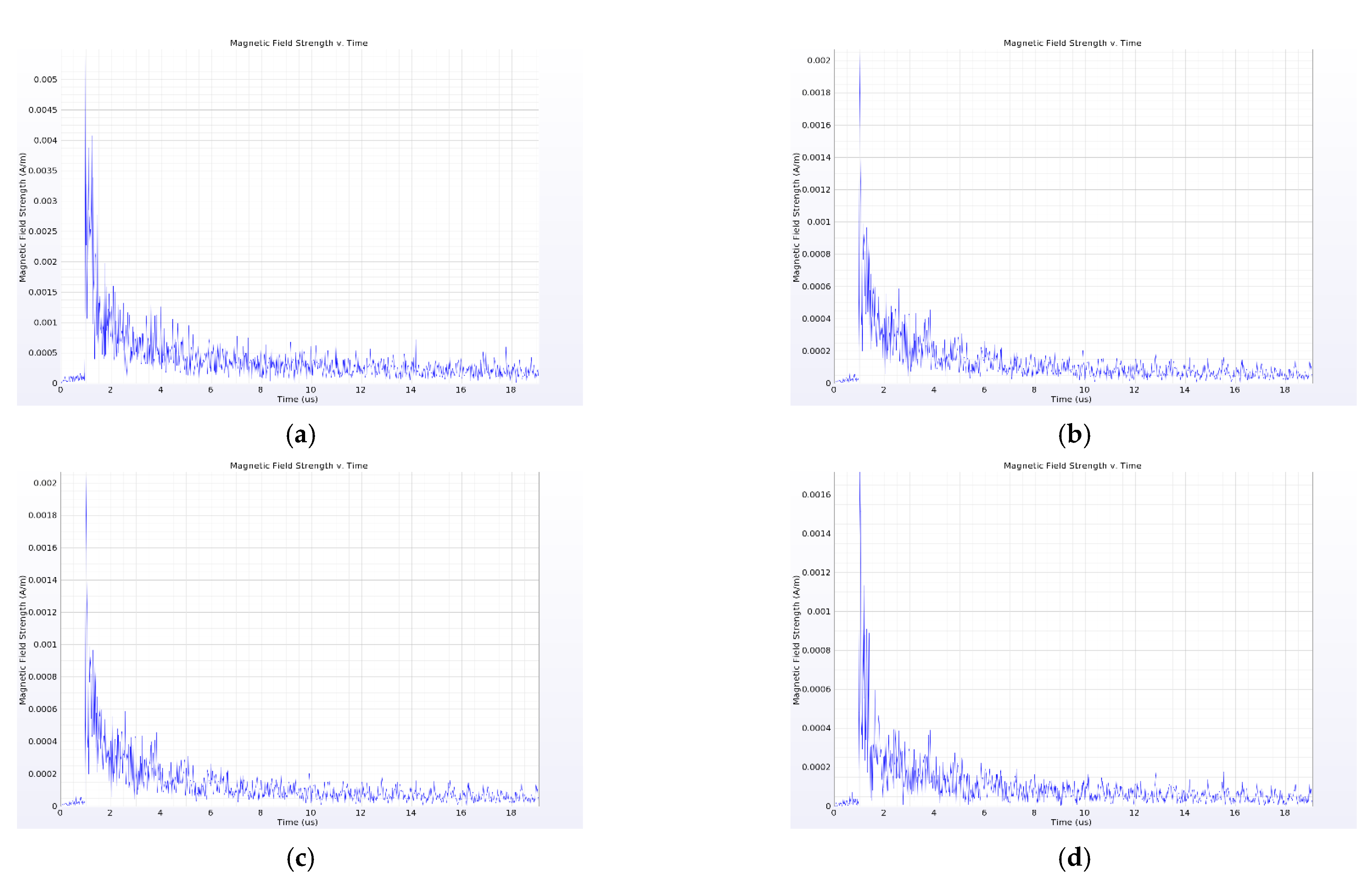
Set the position of the PD excitation source on the surface of the middle of the current transformer; the specific position is (25 mm, −100 mm, 0 mm), and the length of the source is set as 10 mm. Then, place the No. 1 point sensor 15 mm from the front of the source; its specific position is (50 mm, −100 mm, 0 mm). Then, place the No. 2 point sensor 325 mm away from the back of the source, which is close to the cabinet wall on the right side of the switchgear. The specific position is (−300 mm, −100 mm, 0 mm). In the same way, place the sensors at the No. 3 and No. 4 points; their specific positions are (−350 mm, −100 mm, 0 mm), (−400 mm, −100 mm, 0 mm). After placement, the specific position of the source and point sensors around the current transformer is shown in Figure 5. Through these four point sensors, the amplitude of the electric field intensity vector and the magnetic field intensity vector at these four points can be observed, respectively, as shown in Figure 6 and Figure 7.
As can be seen from Figure 6, the amplitude of the electric field intensities observed at point sensors 1, 2, 3 and 4 are 0.75335 V/m, 0.56542 V/m, 0.56271 V/m and 0.45782 V/m, respectively. Similarly, as can be seen from Figure 7, the magnetic field intensity amplitudes observed at point sensors 1, 2, 3 and 4 are 0.0054976 A/m, 0.0020688 A/m, 0.0020556 A/m and 0.0017119 A/m, respectively.
According to the amplitude observed by the sensor at these different points, we can know that the amplitude of the electromagnetic wave signal has been decaying with the increase in the detection distance. The amplitude of the signal before and after passing through the current transformer decays faster than that in the air. According to the analysis in Section 2, although the electromagnetic wave does not attenuate in the current transformer, its propagation path includes the following: air–insulating medium and insulating medium–air, which are two composite interfaces. Because of the different wave impedances of the two media, the secondary electromagnetic wave will have the phenomenon of refraction and reflection on the composite interface, resulting in the attenuation of its amplitude. Nevertheless, the current transformer does not cause obvious signal distortion, but in order to detect a weaker signal, the near-field probe should avoid being placed around the current transformer in the switchgear.

4.2. Influence of Insulator on Near-Field Propagation Characteristics of PD Electromagnetic Wave

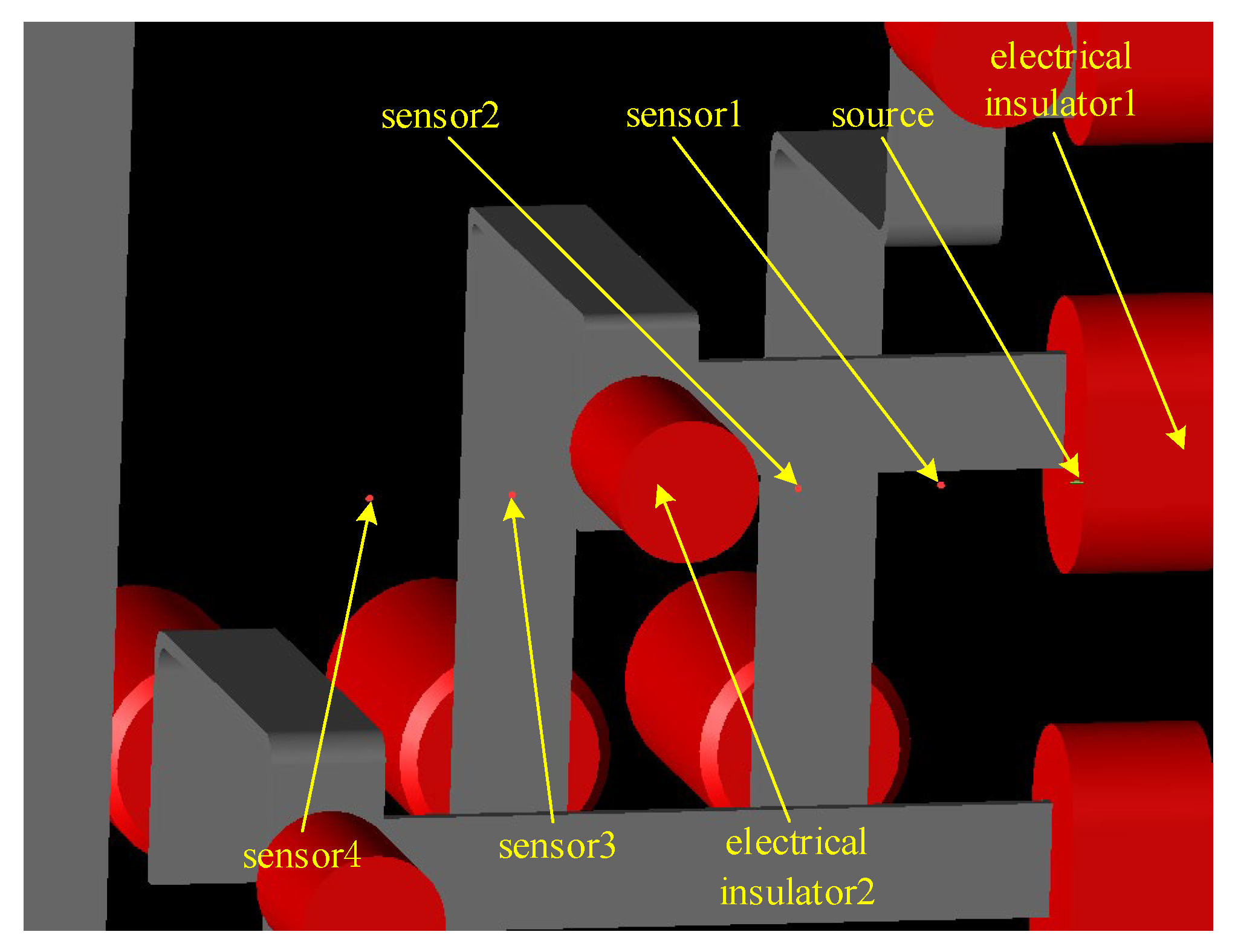
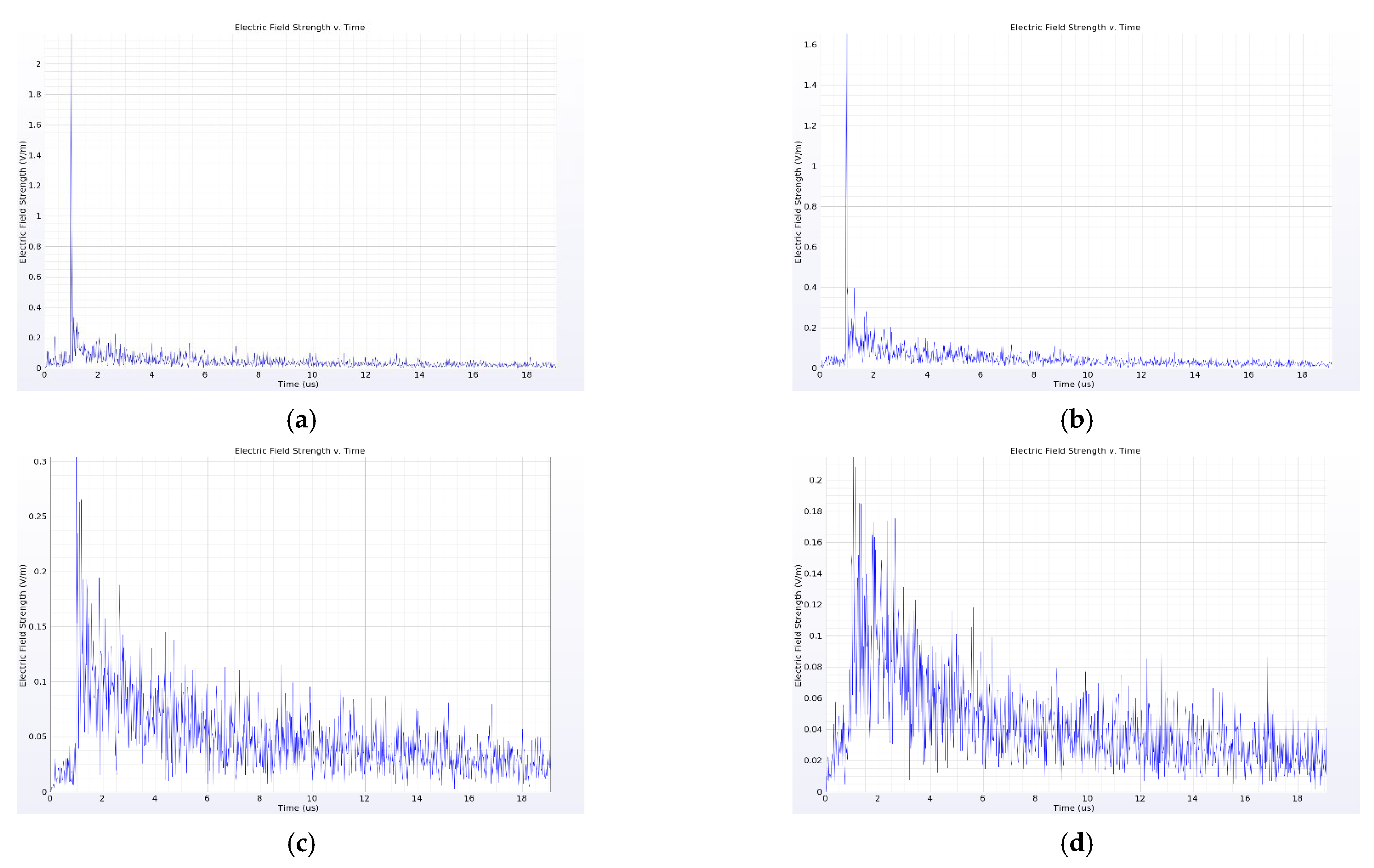
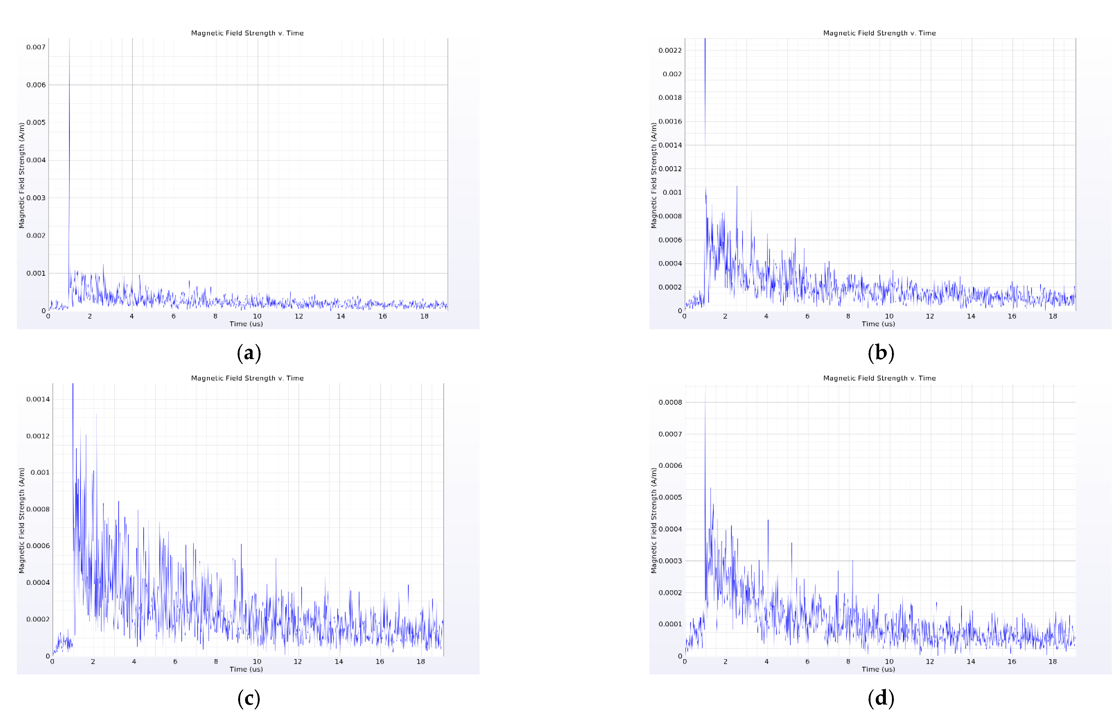
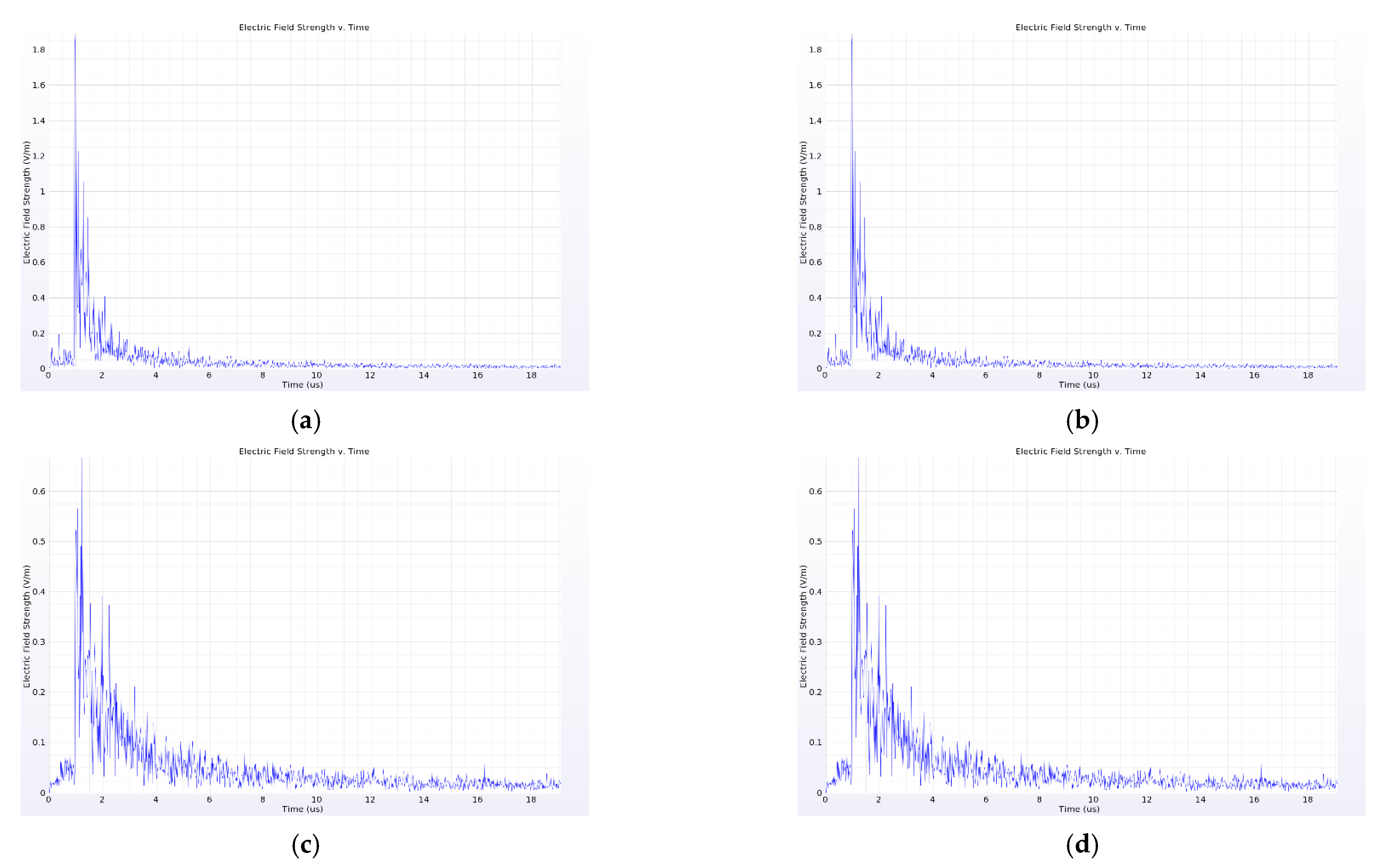
The grid setting and boundary condition setting are consistent with the above simulation settings. As shown in Figure 8, the PD excitation source is re-set on the surface of insulator No. 1; the specific location is (−300 mm, 550 mm, 300 mm), and the source length is set to 10 mm. The insulator between insulator No. 1 and the wall of the switchgear is insulator No. 2. Place point sensor 1 and point sensor 2 between insulators No. 1 and No. 2, respectively, with specific positions of (−300 mm, 550 mm, 200 mm) and (−300 mm, 550 mm, 100 mm). Then, place point sensor 3 and point sensor 4 between insulator No. 2 and the cabinet wall, with specific positions of (−300 mm, 550 mm, −100 mm) and (−300 mm, 550 mm, −200 mm). Through these four sensors, we can observe the changes in the electric field strength and magnetic field strength before and after the PD electromagnetic wave signal passes through insulator No. 2, as shown in Figure 9 and Figure 10.
It can be seen from Figure 9 and Figure 10 that the electric field intensity amplitudes observed at point sensors 1, 2, 3 and 4 are 2.1964 V/m, 1.6506 V/m, 0.30335 V/m and 0.21478 V/m, respectively, and the magnetic field intensity amplitudes observed are 0.007232 A/m, 0.0023032 A/m, 0.0014875 A/m and 0.00085843 A/m, respectively.
By comparing the PD electromagnetic wave signal graph observed at these four points, we can know that when the PD electromagnetic wave signal propagates through the air–insulator and insulator–air interfaces, the amplitudes of both the electric field strength and the magnetic field strength have a large attenuation, which indicates that the electromagnetic wave generates a reflection phenomenon when it propagates to the complex medium interface, resulting in the signal attenuation. In addition, after passing the insulator, the electromagnetic wave signal waveform also has obvious distortion, which has a certain impact on the signal recognition. Therefore, the insulator will not only attenuate the amplitude of the PD electromagnetic wave signal, but will also cause obvious distortion to the signal. Therefore, the near-field probe should not be placed near the insulator.

4.3. Influence of Busbar on Near-Field Propagation Characteristics of PD Electromagnetic Wave

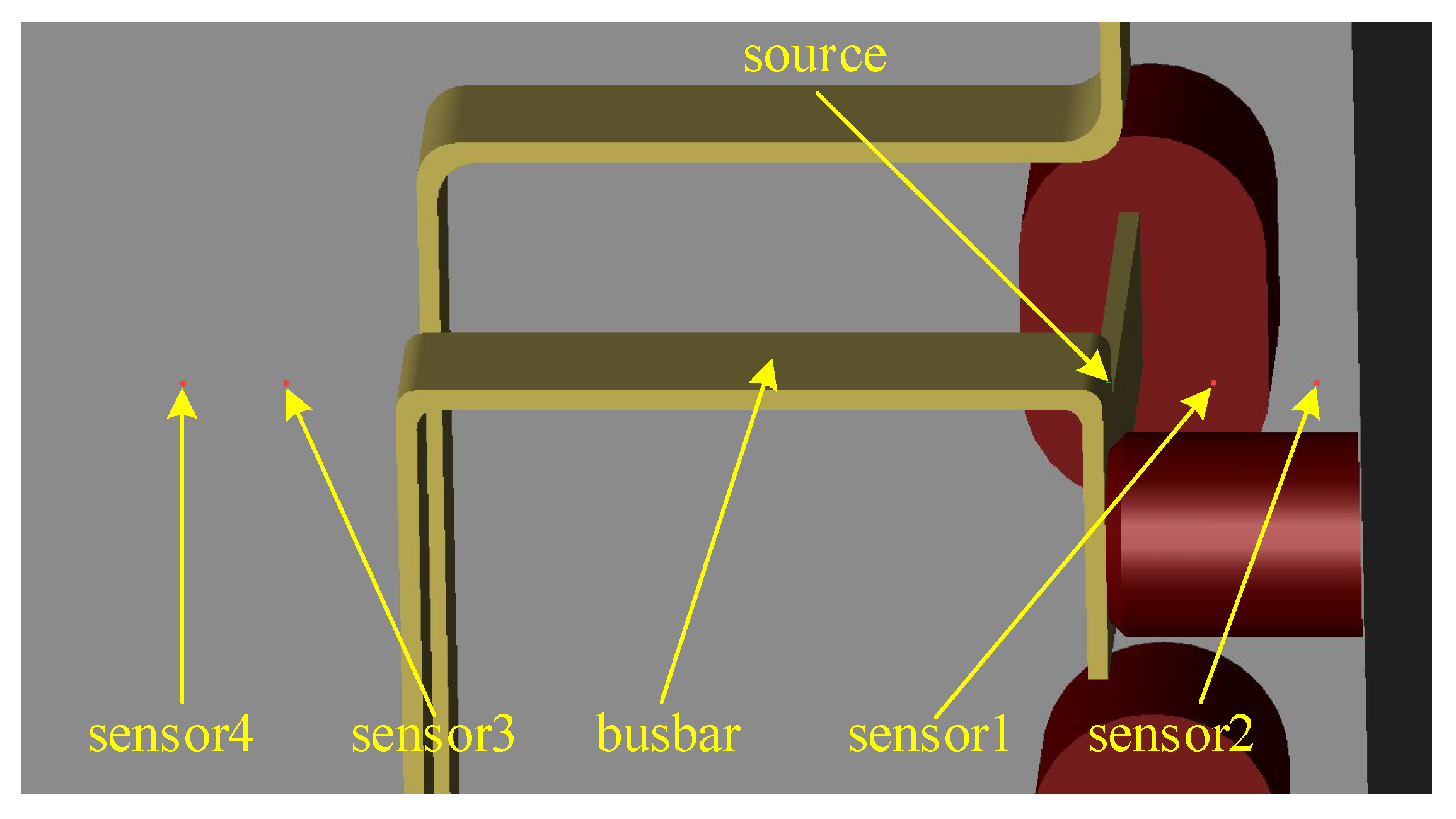
Figure 11 shows the position relationship diagram of the PD excitation source and the point sensor around the busbar. Place the source on the surface of the busbar; the specific location is (−250 mm, 650 mm, 0 mm), and the source length is 10 mm. Place two point sensors, 1 and 2, in the space on the right of the source that are, respectively, (−300 mm, 650 mm, 0 mm) and (−3500 mm, 650 mm, 0 mm). Place point sensors 3 and 4 in the space behind the bus on the left side of the source. The specific positions are (150 mm, 650 mm, 0 mm) and (200 mm, 650 mm, 0 mm), respectively. Through these four point sensors, we can observe the changes in the electric field strength and magnetic field strength of the PD electromagnetic wave signal before and after passing through the bus. See Figure 12 and Figure 13 for details.
It can be seen from Figure 12 and Figure 13 that the amplitudes of the electric field intensity observed at point sensors 1, 2, 3 and 4 are 1.8893 V/m, 1.8817 V/m, 0.66542 V/m and 0.66275 V/m, respectively, and that the magnetic field intensities are 0.0077076 A/m, 0.007689 A/m, 0.0015601 A/m and 0.0015551 A/m, respectively.
Through analysis, we can know that when the near-field electromagnetic wave signal propagates through the busbar, the signal amplitude attenuation is large, but the signal waveform distortion is small. This is because the busbar, σ ω ε = 0.19 , is a general conductor; this means that the influence of the conduction current cannot be ignored. The conducting current will generate joule heat, which will lead to the loss of electromagnetic wave energy. When the electromagnetic wave travels through the busbar, not only the loss caused by the busbar itself, but also the loss caused by the refraction and reflection of the composite interface should be considered. Therefore, the near-field probe should be placed away from the busbar.

4.4. Influence of Switchgear Wall on Near-Field Propagation Characteristics of PD Electromagnetic Wave

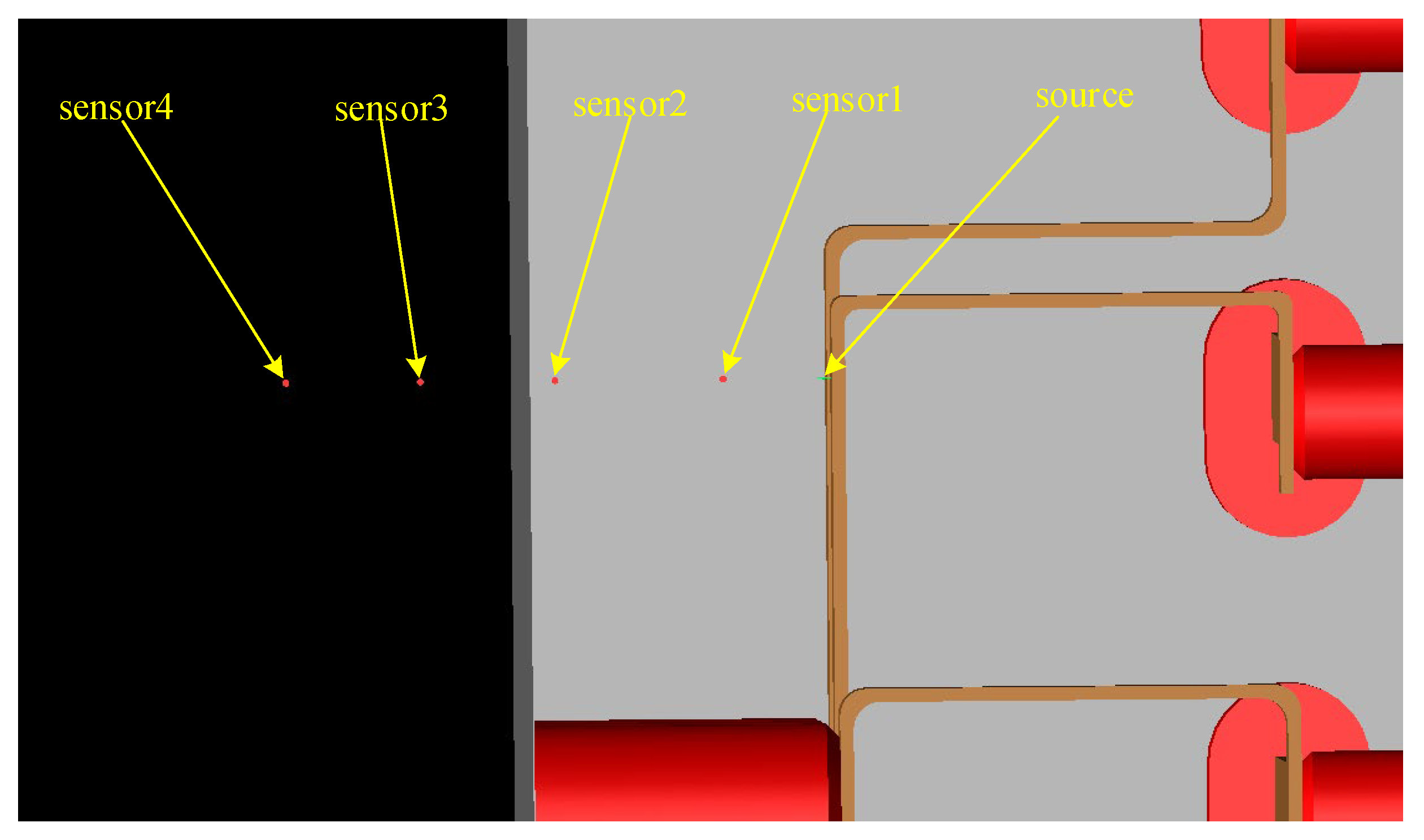
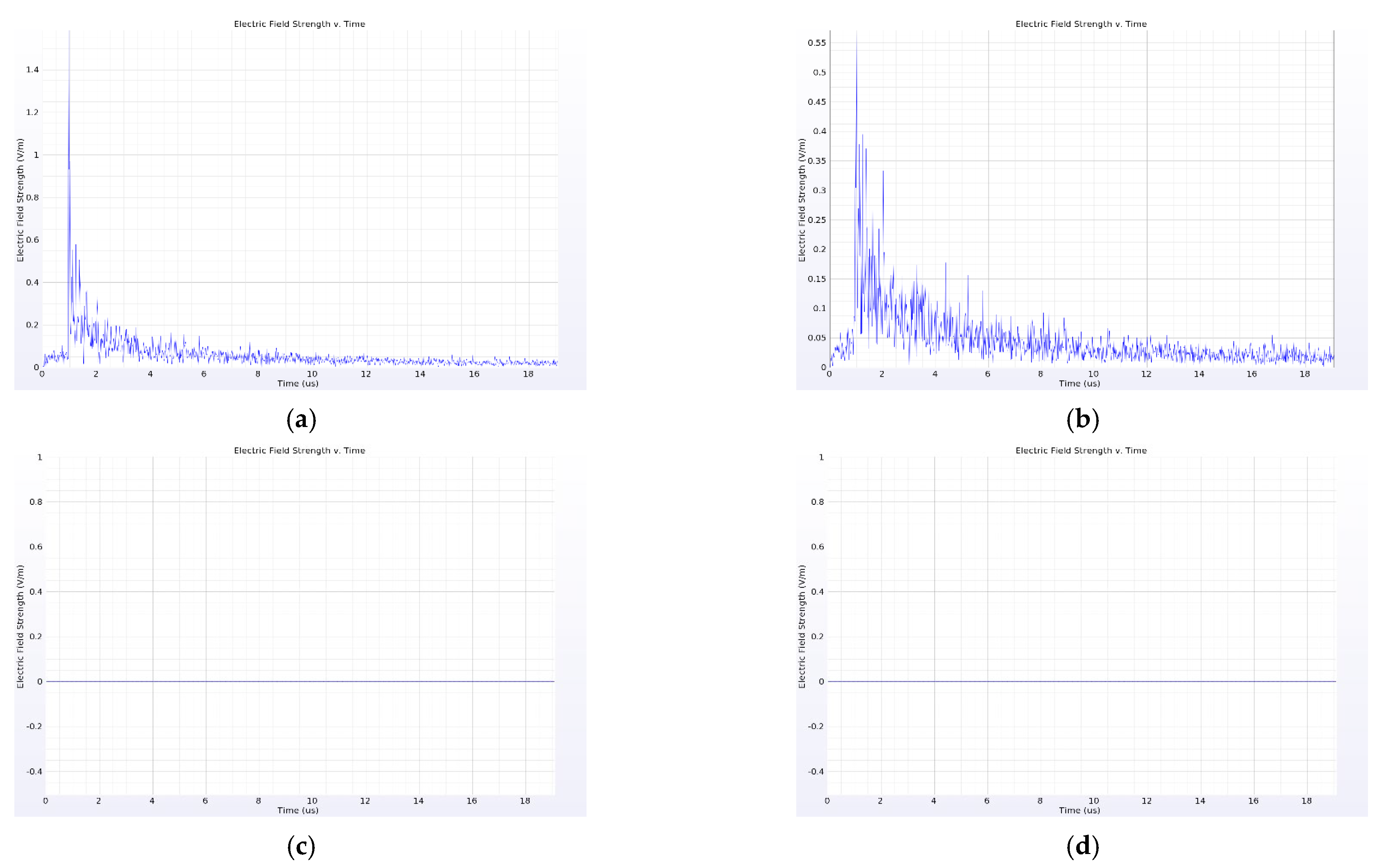
This section researches the influence of the switchgear wall on the near-field propagation characteristics of the PD electromagnetic wave signal. Figure 14 shows the location of the PD excitation source and four point sensors around the cabinet wall of the switchgear. Set the position of the PD excitation source as (95 mm, 600 mm, 0 mm), the source length as 10 mm, and the specific position of point sensors 1, 2, 3, and 4 as (175 mm, 600 mm, 0 mm), (300 mm, 600 mm, 0 mm), (400 mm, 600 mm, 0 mm), (500 mm, 600 mm, 0 mm). Among them, the No. 1 and No. 2 point sensors are inside the switchgear, and the No. 3 and No. 4 point sensors are outside the switchgear. Through these four point sensors, the signal time domain diagram of the PD electromagnetic wave signal before and after passing through the cabinet wall can be observed, as shown in Figure 15 and Figure 16.
It can be seen from Figure 15 that when the PD electromagnetic wave signal is just transmitted, the electric field intensity amplitudes observed by point sensors 1 and 2 are 1.5833 V/m and 0.5713 V/m, respectively. However, point sensors 3 and 4 outside the switchgear did not observe the electric field signal. Similarly, according to Figure 16, the magnetic field intensity amplitudes observed by point sensors 1, 2, 3 and 4 are 0.00075895 A/m, 0.00075601 A/m, 0 A/m and 0 A/m, respectively.
It can be seen from the above two figures that the PD electromagnetic wave signal cannot be detected by the sensor outside the switchgear. This is because the σ ω ε = 0.019 of the switchgear body is a general conductive medium, and the influence of the conductive current cannot be ignored. That is, in this transmission process, the Joule heat of the signal in the conductive medium and the refraction and reflection phenomenon of the composite interface will bring attenuation to the amplitude of the signal. Therefore, if the PD electromagnetic wave signal in the switchgear is to be well detected, the near-field probe is best placed in the switchgear.

4.5. Analysis of Placement Position of Near-Field Probe

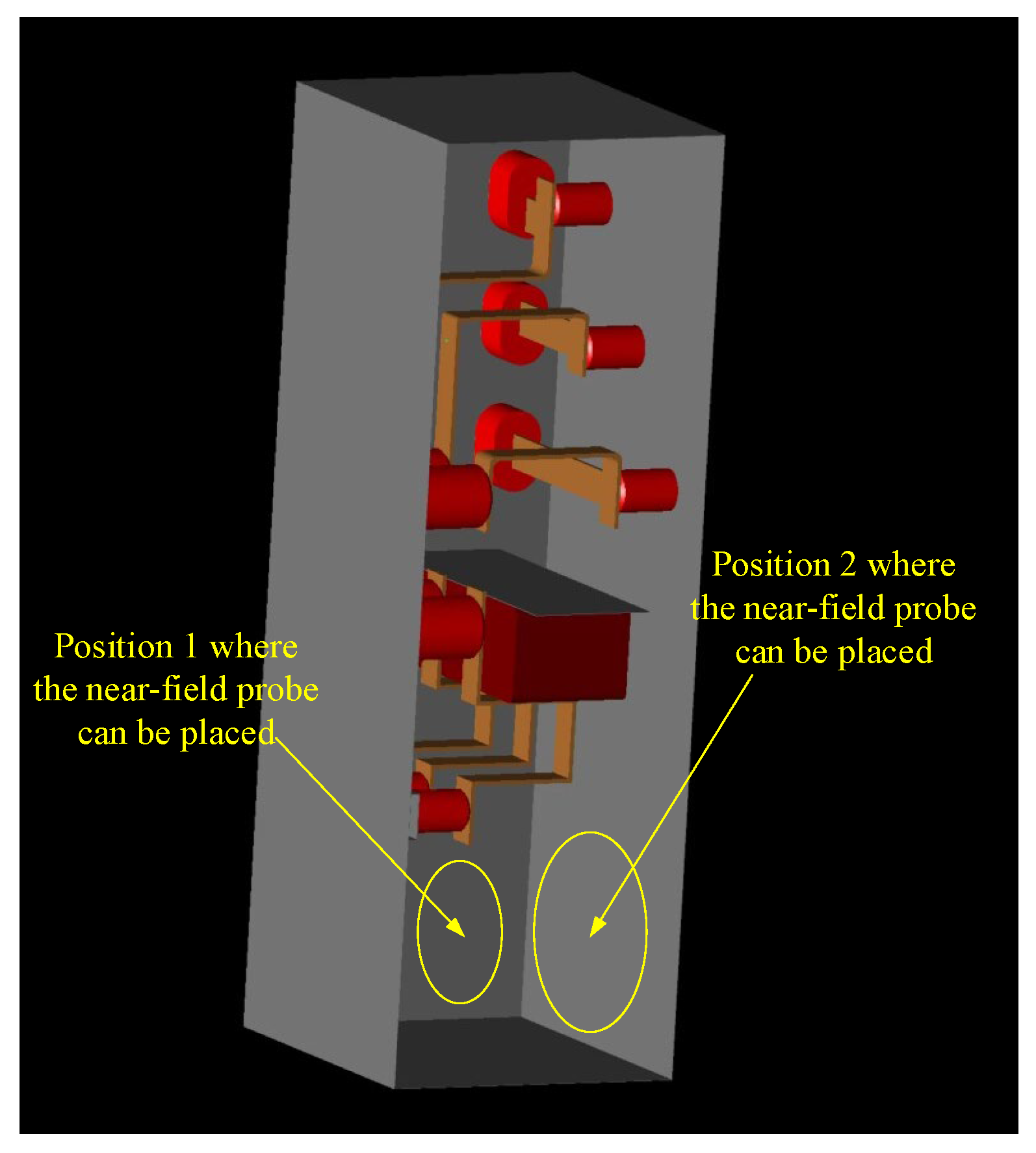
It can be seen from the simulation results in Section 4.1Section 4.4 that the current transformer, insulator, busbar and cabinet body in the switchgear have different effects on the PD electromagnetic wave signal itself, such as attenuation and distortion. When placing the near-field probe, it should avoid being close to the current transformer, insulator and busbar, and should be placed inside the switchgear. According to the above simulation results and the size of the switchgear, the placement positions of the near-field probe are shown in Figure 17, that is, the inner wall and the right wall near the bottom plate of the cabinet.

5. Discussion

Because the energy of the electromagnetic wave signal generated by partial discharge is mainly concentrated in the UHF band, and the position of the partial discharge detection sensor in the switchgear is just in the near-field area of this part of the signal, the study of the near-field propagation characteristics of the electromagnetic wave signal generated by partial discharge in the switchgear is helpful to provide suggestions for the reasonable layout of near-field probes in the switchgear.
In this paper, XFDTD software, based on finite difference time domain analysis, is used to analyze the influence of the current transformer, insulator, busbar and cabinet in the switchgear on the near-field propagation characteristics of partial discharge electromagnetic wave signals. The amplitude of signals decays faster when they pass through the current transformer, insulator, busbar and cabinet compared to when they pass through air. This is because the signal passes through the two composite interfaces of air–component and component–air. Because of the different wave impedances, the signal sees complex refraction and reflection at this composite interface, which leads to its amplitude attenuation. Therefore, in the subsequent installation of the near-field probe, it should be as far away from these components as possible.
However, the research on the near-field propagation characteristics of partial discharge electromagnetic wave signals in the switchgear is limited to theoretical and simulation analysis, and the near-field propagation characteristics of partial discharge electromagnetic wave signals in an actual switchgear are not studied. In addition, this paper only considers the influence of important components in the switchgear, including the current transformer, insulator, busbar and cabinet, on signal propagation characteristics. In order to obtain more accurate results, the switchgear should be modeled more accurately in the future.

6. Conclusions

This paper is the continuation of previous research; as such, through the simulation and theoretical analysis of the near-field propagation characteristics of the PD electromagnetic wave signal in the switchgear, the installable position of the near-field probe is determined.
(1)
Different components in the switchgear have different effects on the near-field electromagnetic wave signal of PD: the current transformer, insulator and busbar have a strong attenuation effect on the amplitude of the near-field electromagnetic wave signal of PD in the switchgear, and the insulator also causes obvious signal distortion, which is not conducive to the subsequent identification of the signal. When installing the near-field probe, it is important to keep away from these three components. In addition, the cabinet wall also causes a large attenuation of the signal, and thus the probe should be installed in the switchgear.
(2)
The near-field probe can be installed on the inner wall or the right wall of the bottom plate of the switchgear.
In the future, we will study the influence of different components on the near-field propagation characteristics of partial discharge electromagnetic wave signals on more accurate switchgear models and a real switchgear.

Author Contributions

Conceptualization, J.Z.; methodology, J.Z.; software, J.Z.; validation, J.Z.; formal analysis, J.Z.; investigation, J.Z.; resources, J.Z.; data curation, J.Z.; writing—original draft preparation, J.Z. and Z.X.; writing—review and editing, J.Z.; visualization, R.L.; supervision, W.Z.; project administration, L.W.; funding acquisition, C.S. and M.H. All authors have read and agreed to the published version of the manuscript.

Funding

“Research and development of new smart sensor technology to promote the development of green energy” (202104BN050011), and “Research and development of key technologies for con-formal implantation of new intelligent power sensing for power grid main equipment” (YN-KJXM20210075).

Conflicts of Interest

The authors declare no conflict of interest.

References

  1. Qi, B.; Li, C.; Xing, Z.; Wei, Z. Partial discharge initiated by free moving metallic particles on GIS insulator surface: Severity diagnosis and assessment. IEEE Trans. Dielectr. Electr. Insul. 2014, 21, 766–774. [Google Scholar] [CrossRef]
  2. Huang, L.; Tang, J.; Ling, C.; Zhang, X. Research on partial discharge pattern recognition based on multi-feature information fusion technology. High Volt. Technol. 2015, 41, 947–955. [Google Scholar] [CrossRef]
  3. Fotis, G.; Vita, V.; Maris, T.I. Risks in the European Transmission System and a Novel Restoration Strategy for a Power System after a Major Blackout. Appl. Sci. 2023, 13, 83. [Google Scholar] [CrossRef]
  4. Liu, J. Cause analysis and solution of insulation failure of 40.5 kV air insulated switchgear. Autom. Today 2018, 5, 46–47. [Google Scholar]
  5. Huang, Y.; Zhang, G.; Yuan, G.; Li, Y. Suspended discharge caused by the suspension of the terminal of the switch cabinet live display sensor. Electr. World 2020, 61, 11–14. [Google Scholar]
  6. Zu, Y.; Zu, L.; Liu, Y. Analysis and treatment of insulation failure of high-voltage switchgear. Henan Electr. Power 2015, 43, 35–39. [Google Scholar]
  7. Cao, P.; Xu, P.; He, J.; Gao, K.; Tian, H.; Ji, Y. Insulation defect detection technology for switchgear based on multi-source perception. China Power 2021, 54, 117–124+133. [Google Scholar]
  8. Suo, C.; Zhao, J.; Wu, X.; Xu, Z.; Zhang, W.; He, M. Partial Discharge Detection Technology for Switchgear Based on Near-Field Detection. Electronics 2023, 12, 336. [Google Scholar] [CrossRef]
  9. Wu, Y.; Zhang, H.; Wu, J.; Zhang, G. Experimental study on the propagation characteristics of UHF partial discharge signals in linear and L-shaped structures for 252 kV GIS. High Volt. Appar. 2022, 58, 223–228. [Google Scholar] [CrossRef]
  10. Darwish, A.; Coapes, G.; Refaat, S.S.; Abu-Rub, H.; Toliyat, H.A. PD Signal Attenuation in 550-kV GIS: Impact of Different Barriers on the Propagation of Electromagnetic Waves. IEEE Trans. Instrum. Meas. 2021, 70, 1–13. [Google Scholar] [CrossRef]
  11. Zhao, T.; Judd, M.D.; Stewart, B.G. Attenuation Characteristics and Time Delay of PD Electromagnetic Wave Propagation in GIS Systems. IEEE Trans. Power Deliv. 2022, 37, 937–946. [Google Scholar] [CrossRef]
  12. Zhang, X.; Zhang, G.; Li, Y.; Zhang, J.; Huang, R. On the Feasibility of Gap Detection of Power Transformer Partial Discharge UHF Signals: Gap Propagation Characteristics of Electromagnetic Waves. Energies 2017, 10, 1531. [Google Scholar] [CrossRef] [Green Version]
  13. Du, J.; Chen, W.; Zhang, Z.; Yang, X. Propagation characteristics of UHF signals of partial discharge in real transformers. High Volt. Technol. 2020, 46, 2185–2191. [Google Scholar] [CrossRef]
  14. Rostaminia, R.; Saniei, M.; Vakilian, M.; Mortazavi, S.S. Evaluation of transformer core contribution to partial discharge electromagnetic waves propagation. Int. J. Electr. Power Energy Syst. 2016, 83, 40–48. [Google Scholar] [CrossRef]
  15. Yao, C.; Huang, C.; Wu, B.; Chen, P.; Chen, Y.; Mi, Y. Analysis of UHF signal propagation characteristics in switchgear cabinet using finite-difference time-domain method. High Volt. Technol. 2013, 2, 272–279. [Google Scholar]
  16. Wang, Y.; Liu, Q.; Lu, G.; Huang, Y. Analysis of the influence of switch cabinet structure on UHF electromagnetic wave propagation characteristics. J. Electr. Technol. 2013, 28, 293–300. [Google Scholar] [CrossRef]
  17. Xu, L. UHF Online Monitoring System and Application of 10 kV Switchgear Discharge; Chongqing University: Chongqing, China, 2016. [Google Scholar]
  18. Yang, K.; Li, W.; Song, G.; Cheng, P. Operation Analysis of HV Switchgears in 2013. Smart Grid 2013, 2, 32–41. [Google Scholar]
  19. Zhang, X.; Li, G.; Huang, R.; Xiang, Z.; Zhao, Y.; Yao, S.; Wang, X. Statistical analysis of defect rate of GIS with different opera-tion years and operation and maintenance suggestions. High Volt. Electr. 2016, 52, 184–188, 194. [Google Scholar]
  20. Xu, Y.; Cheng, J.; Liu, W.; Gao, W. Evaluation of the UHF method based on the investigation of a partial discharge case in post insulators. IEEE Trans. Dielectr. Electr. Insul. 2017, 24, 3669–3676. [Google Scholar] [CrossRef]
  21. Cheng, J.; Xu, Y.; Ding, D.; Liu, W. Investigation of sensitivity of the ultra-high frequency partial-discharge detection technology for micro-crack in an epoxy insulator in GIS. High Volt. 2020, 5, 697–703. [Google Scholar] [CrossRef]
  22. Ouyang, J.; Zhang, Z.; Peng, Z.; Liu, L.; Chen, X. Characteristic radiation spectra of negative corona discharges from air needle tips. High Volt. Technol. 2012, 38, 2237–2241. [Google Scholar]
  23. Liu, W.; Liu, S.; Hu, X.; Yuan, Q. Experimental analysis of radiation characteristics of tip corona discharge. High Volt. Electron. 2008, 1, 20–22. [Google Scholar]
  24. Qiu, C.; Wang, N. (Eds.) Partial Discharge of Electrical Equipment and Its Test Technology; Machinery Industry Press: Beijing, China, 1994. [Google Scholar]
  25. Yee, K. Numerical solution of initial boundary value problems involving maxwell’s equations in isotropic media. IEEE Trans. Antennas Propag. 1966, 14, 302–307. [Google Scholar] [CrossRef] [Green Version]
  26. Tan, W. Optimization algorithm of electromagnetic simulation based on FDTD method. Comput. Eng. Des. 2008, 29, 6362–6364+6396. [Google Scholar]
  27. Chang, W.; Tang, Z.; Li, C.; Wang, C. Simulation analysis of UHF signal propagation characteristics of partial discharge in transformers. High Volt. Technol. 2009, 35, 1629–1634. [Google Scholar] [CrossRef]
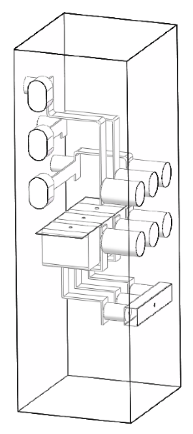
Figure 1. Model of switchgear.
Energies 16 03372 g001
Figure 2. Time-domain waveform of Gaussian pulse current source.
Energies 16 03372 g002
Figure 3. Frequency-domain waveform of Gaussian pulse current source.
Energies 16 03372 g003
Figure 4. PD electromagnetic wave signal received by near-field probe.
Energies 16 03372 g004
Figure 5. Location distribution of source and point sensors around current transformer.
Energies 16 03372 g005
Figure 6. Effect of current transformer on near-field propagation characteristics of PD electromagnetic wave signal. (a) Electric field strength at point sensor 1; (b) Electric field strength at point sensor 2; (c) Electric field strength at point sensor 3; (d) Electric field strength at point sensor 4.
Energies 16 03372 g006
Figure 7. Effect of current transformer on near-field propagation characteristics of PD electromagnetic wave signal. (a) magnetic field strength at point sensor 1; (b) magnetic field strength at point sensor 2; (c) magnetic field strength at point sensor 3; (d) magnetic field strength at point sensor 4.
Energies 16 03372 g007
Figure 8. Location distribution of source and point sensors around insulator.
Energies 16 03372 g008
Figure 9. Effect of insulator on near-field propagation characteristics of PD electromagnetic wave signal. (a) Electric field strength at point sensor 1; (b) Electric field strength at point sensor 2; (c) Electric field strength at point sensor 3; (d) Electric field strength at point sensor 4.
Energies 16 03372 g009
Figure 10. Effect of insulator on near-field propagation characteristics of PD electromagnetic wave signal. (a) Magnetic field strength at point sensor 1; (b) magnetic field strength at point sensor 2; (c) magnetic field strength at point sensor 3; (d) magnetic field strength at point sensor 4.
Energies 16 03372 g010
Figure 11. Location distribution of source and point sensors around busbar.
Energies 16 03372 g011
Figure 12. Effect of busbar on near-field propagation characteristics of PD electromagnetic wave signal. (a) Electric field strength at point sensor 1; (b) Electric field strength at point sensor 2; (c) Electric field strength at point sensor 3; (d) Electric field strength at point sensor 4.
Energies 16 03372 g012
Figure 13. Effect of busbar on near-field propagation characteristics of PD electromagnetic wave signal. (a) magnetic field strength at point sensor 1; (b) magnetic field strength at point sensor 2; (c) magnetic field strength at point sensor 3; (d) magnetic field strength at point sensor 4.
Energies 16 03372 g013aEnergies 16 03372 g013b
Figure 14. Location distribution of source and point sensors around switchgear wall.
Energies 16 03372 g014
Figure 15. Effect of switchgear wall on near-field propagation characteristics of PD electromagnetic wave signal. (a) Electric field strength at point sensor 1; (b) Electric field strength at point sensor 2; (c) Electric field strength at point sensor 3; (d) Electric field strength at point sensor 4.
Energies 16 03372 g015
Figure 16. Effect of switchgear wall on near-field propagation characteristics of PD electromagnetic wave signal. (a) magnetic field strength at point sensor 1; (b) magnetic field strength at point sensor 2; (c) magnetic field strength at point sensor 3; (d) magnetic field strength at point sensor 4.
Energies 16 03372 g016aEnergies 16 03372 g016b
Figure 17. Position in which the near-field probe can be placed.
Energies 16 03372 g017
Table 1. Material parameters of components of switchgear.
Switchgear Elements Relative   Permittivity   ε r Relative   Permeability   μ r Conductivity   σ / ( S m 1 )
cabinet1- 5.6 e 6
busbar1- 5.7 e 7
CT3.6- 1 e 8
insulator5.7- 1 e 8
Disclaimer/Publisher’s Note: The statements, opinions and data contained in all publications are solely those of the individual author(s) and contributor(s) and not of MDPI and/or the editor(s). MDPI and/or the editor(s) disclaim responsibility for any injury to people or property resulting from any ideas, methods, instructions or products referred to in the content.