Article

A Novel ZVS/ZCS Push-Pull LC Resonant DC-DC Converter for Energy Sources

Department of Electrical Engineering, National Taipei University of Technology, 1, Sec. 3, Zhongxiao E. Rd., Taipei 10608, Taiwan
*
Author to whom correspondence should be addressed.
Energies 2023, 16(6), 2892; https://doi.org/10.3390/en16062892
Submission received: 5 February 2023 / Revised: 15 March 2023 / Accepted: 18 March 2023 / Published: 21 March 2023

Abstract

:
In this paper, a novel soft switching push-pull LC resonant DC-DC converter for energy sources is presented. In a high step-up converter, the input of primary side possesses low voltage and high current, so the losses caused by the current account for most of the total power loss. At the same time, the high-voltage stress of the high-voltage output components on the secondary side is also a major problem. Therefore, a high-gain isolated push-pull converter with a secondary-side resonant circuit is proposed, so that the primary-side switches have zero voltage switching (ZVS) and the secondary-side diodes have zero current switching (ZCS). The push-pull structure can reduce the number of active switches, so that the total power loss on the primary side can be reduced. The converter has a resonant tank circuit arranged between the secondary side of isolation transformer and the high-voltage output rectification module. The high-voltage output rectifier module adopts a full-bridge architecture suitable for high-voltage coupling connection. The low-side power switching module adopts a push-pull architecture suitable for low-voltage and high-current applications. The resonant tank circuit uses an inductor–capacitor (LC) structure to improve the resonant tank circuit, which achieves soft switching during power transfer, increasing the efficiency of the converter and improving the electromagnetic compatibility. The main advantage of this technology is that the secondary-side leakage inductance of transformer and the resonant capacitance are connected in series to achieve ZVS for switches and ZCS for diodes. Finally, a prototype of a high-gain push-pull resonant converter was established. The converter was operated at a fixed switching frequency of 135 kHz and a duty cycle of approximately 0.5. The efficiency of the converter can reach 97.1% under experimental tests at an output voltage of 400 V and a rated output power of 500 W.

1. Introduction

In addition to energy supply and demand and economic cost-effectiveness, energy development is also crucial to the protection of and its impact on the environment. According to the development experience of various countries, the occurrence of energy and environmental disasters can significantly impact the direction of energy policy. In the face of multiple challenges of energy security and global warming, policymakers must consider carefully how to protect energy supply security and sustain the environment while promoting economic and energy industry development. Increasing revenue and reducing expenditure have become the two most important axes. Between them, increasing revenue should focus on the development of low-carbon energy sources, while reducing expenditure should improve the efficiency of energy usage and conversions. However, renewable energy [1] has low energy density and high generation costs. In addition, most of the renewable energy sources are intermittent. Without the support of neighboring power grids, it is necessary to invest in building energy storage facilities to ensure power stability. The battery energy storage system (BESS) [2] serves as a power storage unit for different sources of energy, such as solar, wind, geothermal, ocean energy, etc. By integrating storage elements into the renewable energy system, the variability and intermittency concerns caused by the integration of renewable energy into the grid can be reduced to some extent. In addition to being used for local self-consumption, the BESS can also be used to provide ancillary services (A/S) [3], which can also bring flexibility of distributed generation (DG) to consumers.
In recent years, many topologies of non-isolated and isolated DC-DC converter have been released and applied to green energy power conversion devices. Among these, non-isolations have some limitations, such as the output current discontinuity, high output ripple and duty cycle constraints as described in the literature [4], so they are not suitable for high voltage gain. As described in the literature, the use of cascaded multi-stage converter [5], the multi-level switching element [6,7] or the use of isolated inductors [8] increase the number of components and the complexity of the control methods, leading to increased cost and reduced efficiency. Another method to increase the output voltage is to use an isolation transformer. Among these, there are many potential topologies, such as traditional pulse width modulation (PWM) control for full-bridge, half-bridge bridge and push-pull converters or phase-shift controlled for full-bridge converters, which are commonly used in the high-power system with low-voltage inputs. As described in the literature [9], the buck-boost full-bridge converter (BBFB) is a combination of the phase-shift full-bridge (PSFB) and hybrid control methods. The literature [10] describes a method to combine a PSFB with a half-bridge LLC resonant converter, which controls the inductance–inductance–capacitance (LLC) converter with fixing switching frequency and cascades the full-bridge output with controlling phase shift to regulate the output. The literature [11] describes the use of multiple converters to increase voltage gain by connecting the low-voltage input terminal in parallel with interleaved current feeding method and the high-voltage output terminal in series. These converters achieve high voltage gain by increasing the number of switching components and using complex control methods. Despite this, the traditional push-pull converters are still widely used in the industry of low and medium power converters such as uninterruptible power systems (UPS) [12] because they have the advantage of two low-side driven on primary-side switches compared to half-bridge or full-bridge converters. In addition, resonant converters have become more popular in recent years due to the zero- voltage switching (ZVS) of the primary-side switch and the zero-current switching (ZCS) of the output rectifier diode, which reduces the switch and diode switching loss of the converter [13]. In the future, DC-DC converters with high-frequency switch will become the preferrable choice [14] in order to achieve high power density and low cost. High-frequency soft-switching technology can achieve better component utilization, decrease component switching losses and reduce the size and cost of the associated heat sink.
In traditional push-pull converters, including voltage-fed and current-fed converters, the switches on the primary side suffer from high voltage stress during switching, and the diodes on the secondary side suffer from reverse recovery current loss during the turn-off. In addition, the transient high-frequency resonance of the transformer leakage inductance and the switch parasitic capacitor will lead to high switching loss, causing the need to use components with higher rated voltage, thereby reducing the conversion efficiency and affecting the power density and volume of the converter. In order to solve these problems, based on the boost topology converter with passive clamp snubber, the literature [15] studies and analyzes the traditional resistor–diode–capacitor (RDC) clamp snubber, but the improvement of its efficiency is still limited. In addition, the literature [16] uses the active clamp snubber of the active switching element to effectively clamp the voltage of the element to achieve zero voltage switching (ZVS) of the switches during conduction. However, it requires additional floating switching elements and control circuits, making the control more complex and reducing the voltage gain of the converter. At the same time, it also requires additional printed circuit board (PCB) area. In the literature [17], an active clamping circuit is added to the PWM current-fed push-pull converter to suppress surge voltage, enabling the switch to turn with ZVS. However, for current-fed topologies, a larger input inductor [18] is usually required; a higher-rated voltage switch and the switching duty cycles of the two switches need to overlap, resulting in increased conduction losses by the converter, and duty cycles are reduced. A new inductance–capacitance–inductance (LCL) resonant converter topology is described in [19], where the resonant LCL component is located on the primary side of the push-pull converter. There are several disadvantages in this design. The switches of the converter operate at near-resonant frequency, and the switching frequency is set at an even number of the resonant frequency, so that the primary-side switch can achieve quasi-zero voltage switching. Furthermore, the resonant LCL components are located on the primary side with low voltage, so the resonant inductor needs to withstand high current stress.
As far as the high step-up LLC resonant converter are concerned, the design of the high-power level step-up LLC converter places the resonant tank on the low-voltage side, so the resonant devices need to withstand high current stress. Therefore, the design of high step-up converters is currently only used in low power applications [20]. However, if the traditional resonant tank is simply modified in structure, the main idea is to place the resonant tank on the secondary side with high voltage and low current side, so that the current stress of the resonant tank will be smaller than the traditional design. The structure of the resonant circuit on the low current side can be divided into fixed frequency control and variable frequency control. The fixed frequency control described in [21,22] means that the converter operates at a fixed switching frequency and a duty cycle of approximately 0.5, and the output voltage decreases with increasing load; this approach is suitable for voltage-unregulated low to high voltage power converter topologies. On the other hand, in [23], variable frequency control is used to control the high-gain push-pull converter, called high step-up push-pull multi-resonant converter (HSPPMRC), in which both the leakage inductance of the transformer and the parasitic capacitance of the rectifier diode considered as an equivalent capacitance are connected in parallel to achieve resonant tank for soft switching of the switches. However, the voltage range that can be adjusted within the variable frequency control range is small.
In recent years, pulse frequency modulation (PFM) control technology has been used in resonant converters to achieve zero-voltage zero-current switching (ZVZCS) and maintain stable regulation of output voltage. In [24,25], in order to use pulse frequency modulation in the voltage-fed resonant push-pull converter, an auxiliary inductor in parallel is added between the secondary-side resonant tank and the output rectified circuit to achieve the characteristics of LLC resonance. As for [24], the voltage gain M of the LC-SRC resonant tank is less than one, so an auxiliary inductor is added in parallel with the output load to increase M by changing the impedance of the output load of the resonant tank when the switching frequency is changed. Due to the addition of this auxiliary inductor, the efficiency around the rated load is reduced. In addition, the work in [26] presents an H-bridge converter with soft switching based on coupled inductors, the work in [27] proposes an H-bridge converter with adaptive fuzzy-based stability control, and the work in [28] proposes an H-bridge converter with duplex PD inertial damping control.
In this paper, in order to solve the problem of parallel auxiliary inductance setting in [24,25] and the problem of small adjustable range of output voltage within variable frequency control in [23], a resonant push-pull converter based on an inductance–capacitance series resonant converter (LC-SRC) is proposed by changing the position of the LC resonant tank. This converter has high voltage gain and combines the wide voltage characteristic of PWM control of a traditional push-pull converter with the LC-SRC resonant characteristics. This LC-SRC converter, besides all the advantages of the resonant characteristic, also has the following advantages:
  • ZVS of the primary-side switch and ZCS of the output diode can reduce switching losses and improve efficiency.
  • Compared with the half-bridge architecture, all primary-side switches are driven by low-side gate drivers, no floating gate driver is required, which simplifies the drive circuit design and reduces costs.
  • The duty cycle of the switching frequency is adjusted to be close to 0.5 to maximize device utilization.
  • A resonant capacitor connected in series with the secondary-side winding can isolate the DC current to avoid transformer magnetic saturation.
The rest of this paper will be described as follows: In Section 2, the basic operating principle and related theoretical derivation of the proposed LC resonant push-pull converter topology are introduced. In Section 3, the introduction of the series-resonant converter circuit analysis is described. In Section 4, the parameter design of the converter is presented. In Section 5, the simulation and experimental results of the 500 W prototype are presented, and a comparison of different resonant converters in high voltage gain applications is presented. In Section 6, the conclusion is made.
In the following section, the proposed converter topology along with the associated theory will be introduced.

2. Proposed LC-Resonant Push–Pull Converter Topology

2.1. Topology Description

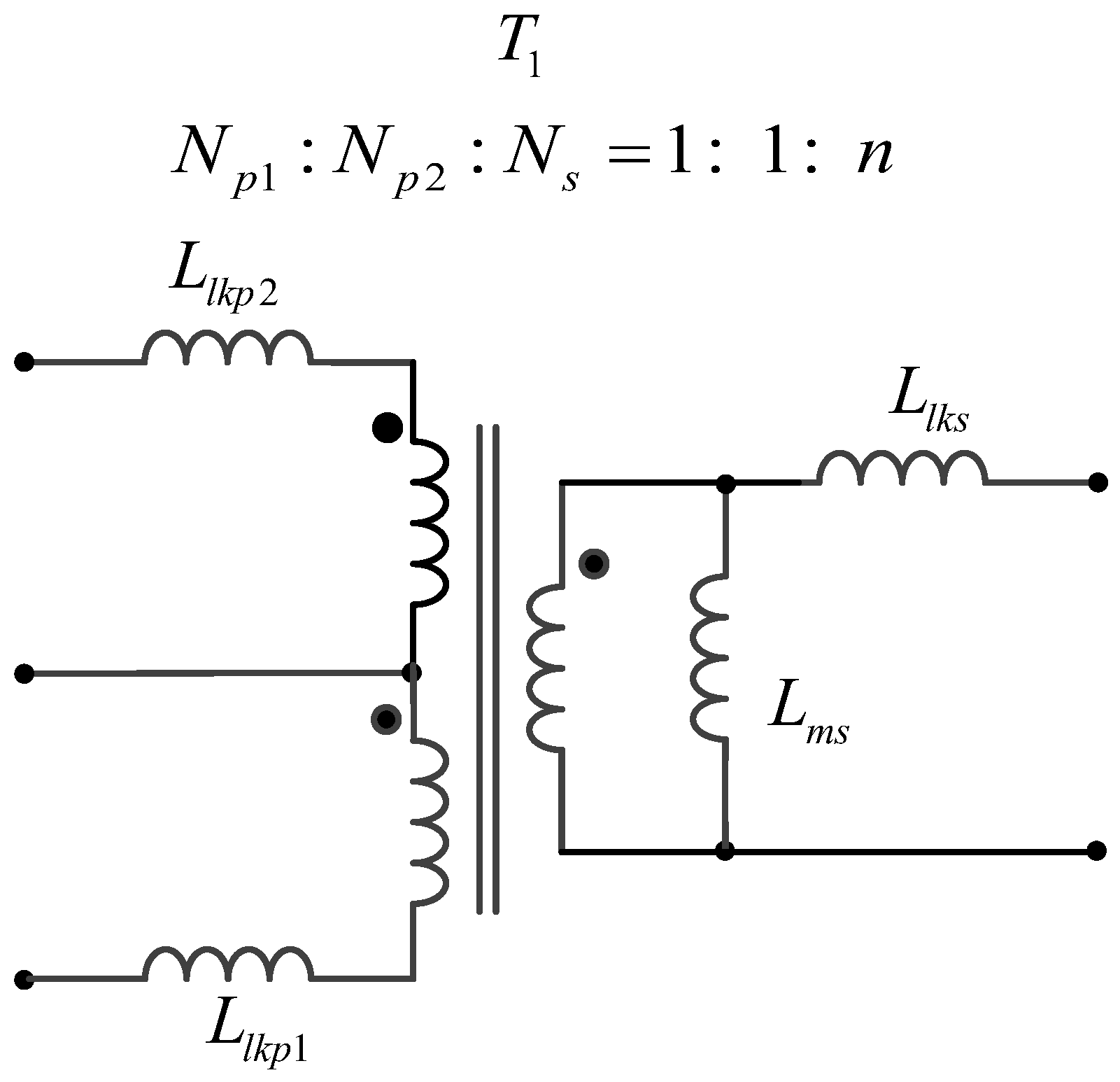
Figure 1 illustrates the high-voltage gain zero voltage switching push-pull resonant converter in this paper. The main circuit consists of power switches, a high-frequency center-tapped transformer, a resonant circuit, a full-bridge rectifier, output capacitors and a resistive load. The main switch of the ZVS push-pull resonant converter consists of bidirectional two-quadrant switches S1 and S2 with a duty cycle of nearly 0.5. Each switch consists of a Metal Oxide Semiconductor Field Effect Transistor (MOSFET), a body diode, and drain-source parasitic capacitances Cs1 and Cs2. The switches can conduct positive or negative current. There is a high-frequency center-tapped transformer T1 at the push-pull primary winding. The equivalent circuit model of transformer is shown in Figure 2. The resonant inductance Lr is composed of the secondary winding leakage inductance Llks of the high-frequency transformer and two primary winding leakage inductances Llkp1 and Llkp2 of high-frequency transformer; Llkp1 and Llkp2 are much smaller than Llks and can be neglected. Therefore, the secondary-side leakage inductance of the high-frequency transformer Llks can be regarded as the resonant inductor Lr and the resonant capacitor Cr connected in series to form a resonant circuit. The parameter value of leakage inductance depends on the physical construction, such as magnetic material, air gap and coil winding technology because the magnetizing inductance Lms of the high-frequency transformer is very large. Therefore, the magnetizing current can be neglected. The series resonant network is fed by the square wave output voltage from the secondary side of the high frequency transformer. After passing through Lr and Cr, the current becomes a sinusoidal wave at the resonant frequency to achieve soft switching operation. The full-bridge rectifier is used to rectify the sinusoidal current and smooth the output voltage through a large-capacitance filter. Therefore, the output voltage Vo can be considered constant and provides a load resistance RL. As for the output voltage regulation, it is controlled by changing the duty cycle of the switching frequency.
Before proceeding with the circuit analysis, some relevant symbols shown in Figure 1 and some required assumptions will be defined as follows:
(1)
Cin and Co are used as the voltage-stabilizing capacitors for the input and output of the converter. The capacitance is large enough to keep the voltage stable at a fixed voltage, and the corresponding voltage signs are defined as VCin and VCo.
(2)
Vin is the input voltage and Vo is the output voltage.
(3)
Iin is the input current and Io is the output current.
(4)
ip, iS1 and iS2 are the input current on the primary side, the current in the switch S1, and the current of the switch S2, respectively.
(5)
iLr and iLm are the output current and magnetizing current of the secondary-side transformer, respectively; iD1, iD2, iD3 and iD4 are the current flowing through the output rectifier diodes D1, D2, D3 and D4, respectively.
(6)
vLr and vT1 are the voltage on the resonant inductance and the output voltage on the secondary side of the transformer, respectively; vCr is the voltage on the resonant capacitor; vD1, vD2, vD3 and vD4 are the voltages across the output rectifier diodes D1, D2, D3 and D4, respectively.
(7)
n is named turns ratio and defined as the number of the secondary-side turns Ns divided by the number of the primary-side turns Np (=Np1 = Np2).

2.2. Series-Load Resonant Converter Analysis

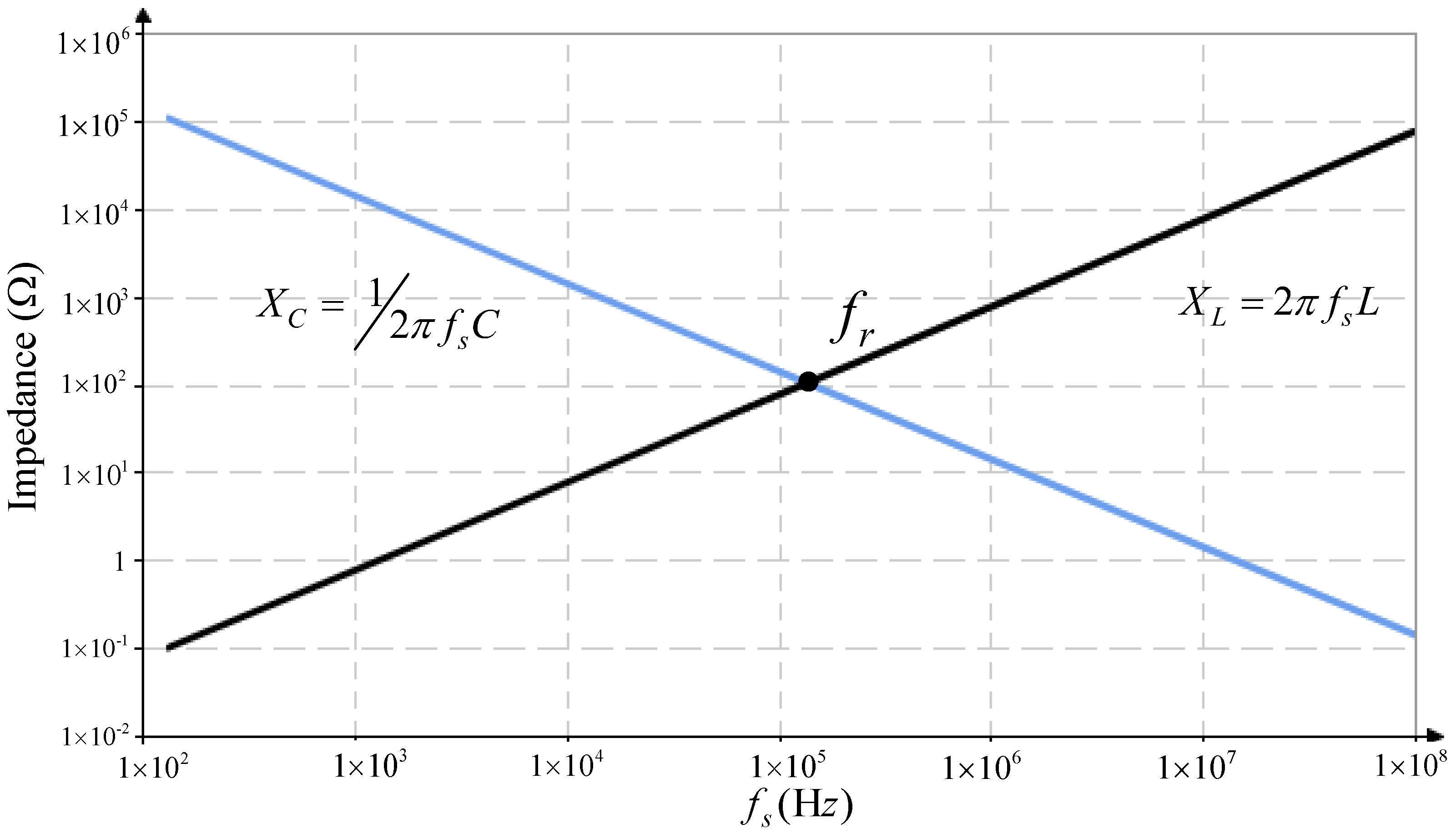
The proposed LC-SRC resonant converter can reduce electromagnetic interference and harmonic distortion because it operates at the resonant frequency with the inductive reactance of the resonant inductor Lr which is equal to the capacitive reactance of the capacitor Cr. The characteristics of the series resonance impedance are shown in Figure 3. The resonant tank operating at the resonant frequency fr has the least impedance, and the resonant tank is used to generate a sinusoidal current output, which will ensure that the resonant tank flows to the output at the maximum power. Meanwhile, the associated parameters are defined as follows:
Z r = L r C r
ω r = 1 L r C r
f r = 1 2 π L r C r
where Zr is the characteristic impedance and ωr is the resonant radian frequency.
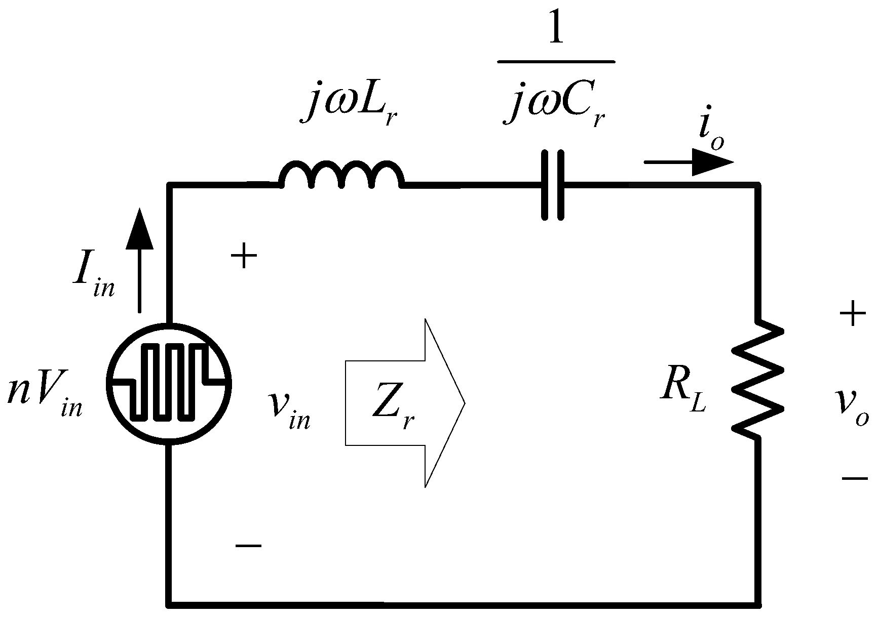
As shown in Figure 4, the load resistor RL is connected in series in the resonant network to form a series resonant tank of the inductance Lr, the capacitor Cr and the resistor RL. If the frequency of the output square wave voltage on the secondary side of the high-frequency transformer is fs, the LC of the series resonant network has the function of filtering and only allows the current of fundamental wave to pass through, so the resonant circuit generates a sinusoidal output current. The resonant equation for voltage and current is as follows:
v i n = n V i n sin ( ω r t + θ v )
i o = I i n sin ( ω r t + θ i )
The impedance Zr of this resonant network when seen to the right from the input voltage is as follows:
Z r = R L + j ( ω r L r 1 ω r C r )
The magnitude of the characteristic impedance, called ||Zr||, and the corresponding phase angle θZr are as follows:
Z r = R L 2 + ( ω r L r 1 ω r C r ) 2
θ z r = tan 1 ( ω r L r 1 ω r C r R L )
θ z r = θ v θ i
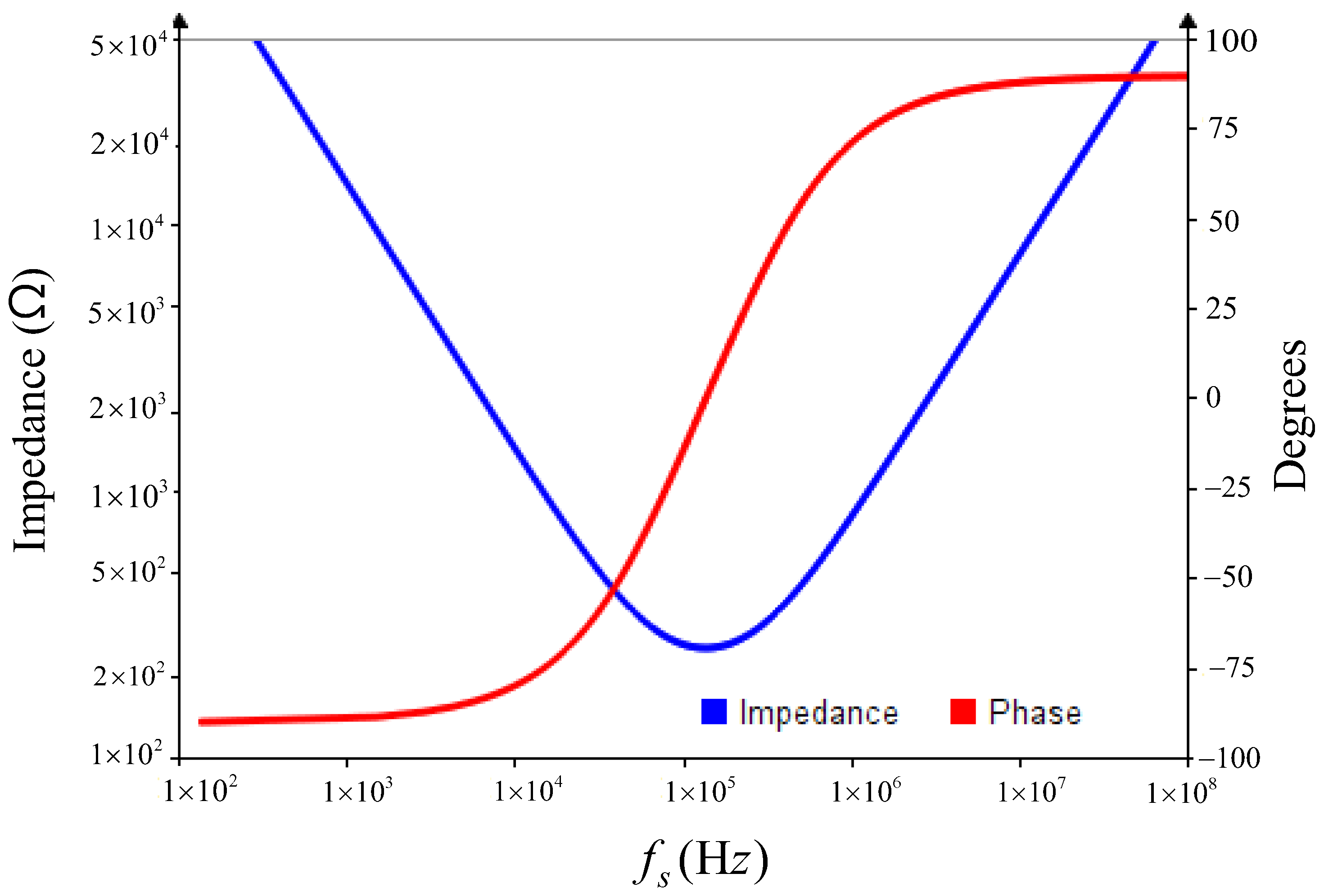
Shown in Figure 5 are the magnitude of the characteristic impedance ||Zr|| of the resonant network, the relationship curve between the phase angle θZr and switching frequency fs. It can be seen that when the switching frequency fs of the power supply is equal to the resonant frequency fr, the magnitude of the characteristic impedance of the resonant network is ||Zr|| = RL; when the switching frequency fs is lower than the resonant frequency fr, the resonant circuit presents capacitive reactance, θZr < 0. The resonant inductor current leads the resonant capacitor voltage. When the switching frequency fs is higher than the resonant frequency fr, the resonant circuit presents inductive reactance, θZr > 0; the resonant inductor current lags the resonant capacitor voltage.
The ratio of the output voltage vo to the input voltage nvin of the series resonant network and the angular frequency ωr is expressed as follows:
v o n v i n = R L R L 2 + ( ω s L r 1 ω s C r ) 2
ω s = 2 π f s
The frequency characteristic of the series resonant circuit can be described by the quality factor Q, which is defined as follows:
Q = Z r R = ω r L r R L = 1 ω r R L C r
ω r = 2 π f r = 1 L r C r
Therefore, the ratio of the output voltage vo to the input voltage nvin cab be expressed as follows:
v o n v i n = 1 1 + Q 2 ( ω r ω s ω s ω r ) 2
Figure 6 shows the relationship between the ratio of the output and input under the normalized radian frequency with the quality factor taken into account. If the switching radian frequency is fixed, the higher the quality factor, the smaller the voltage on the load resistance. Moreover, increasing the inductance Lr and decreasing the capacitance Cr can increase the quality factor Q.
In following section, the basic operating principles along with the relevant formulas will be described.

3. Circuit Analysis

The proposed set-up converter, shown in Figure 1, consists of a push-pull converter and a full-bridge rectifier. Switches S1 and S2 alternate operating with a duty cycle of approximately 0.5. It will work in full load mode to reduce the current stress of the switch and achieve zero current of diode turn-off. To simplify the analysis, the following assumptions are made.
  • Switches S1 and S2 are ideal, but the body diodes of the switches are DS1 and DS2, respectively.
  • The turns ratio of the high frequency transformer is 1:1:n and is modeled as an ideal transformer with magnetizing inductance Lms, leakage inductance Llks, Llkp1 and Llkp2.
  • Because the output capacitor Co is large enough, the output voltage of Vo is constant.
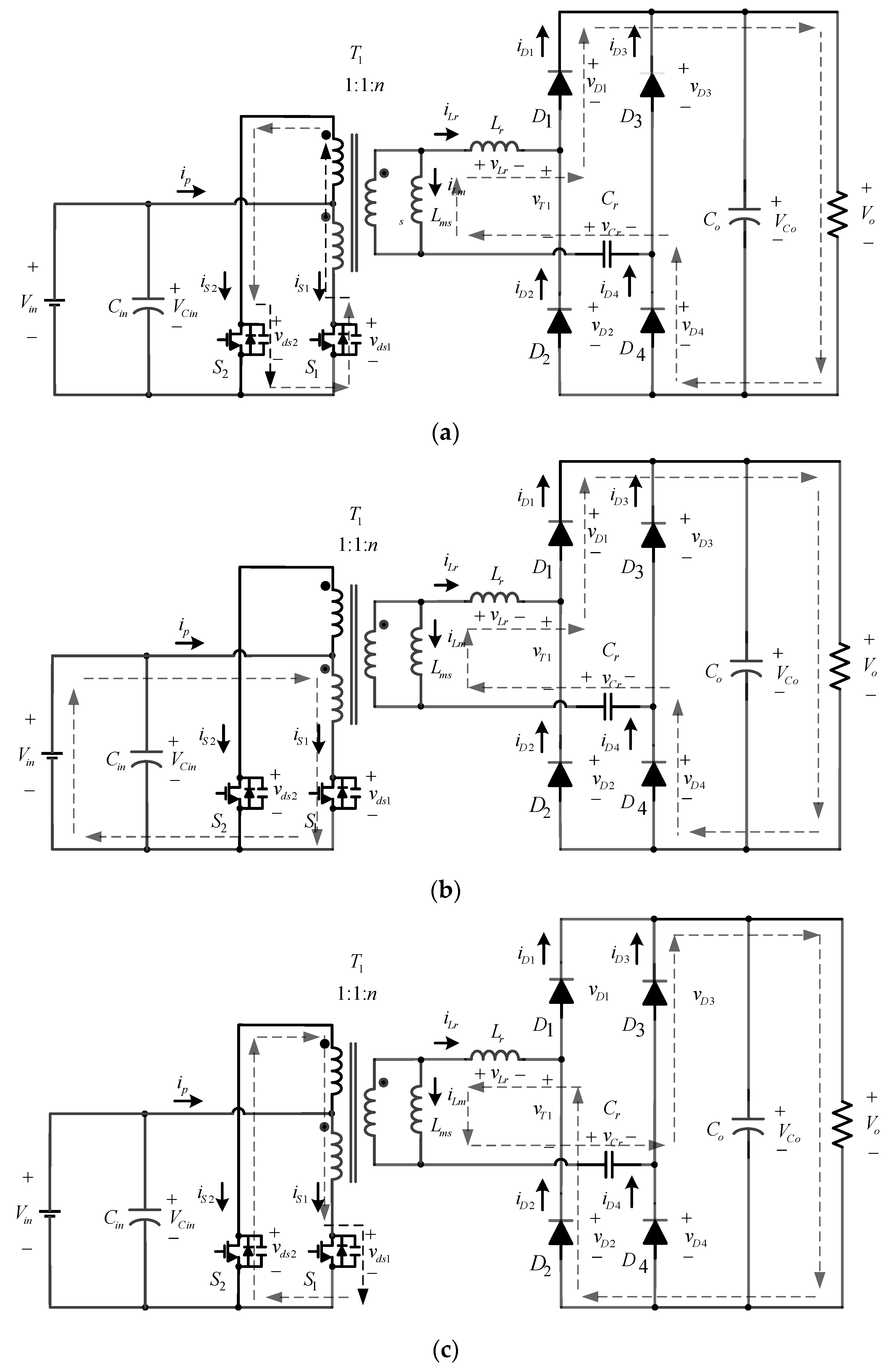
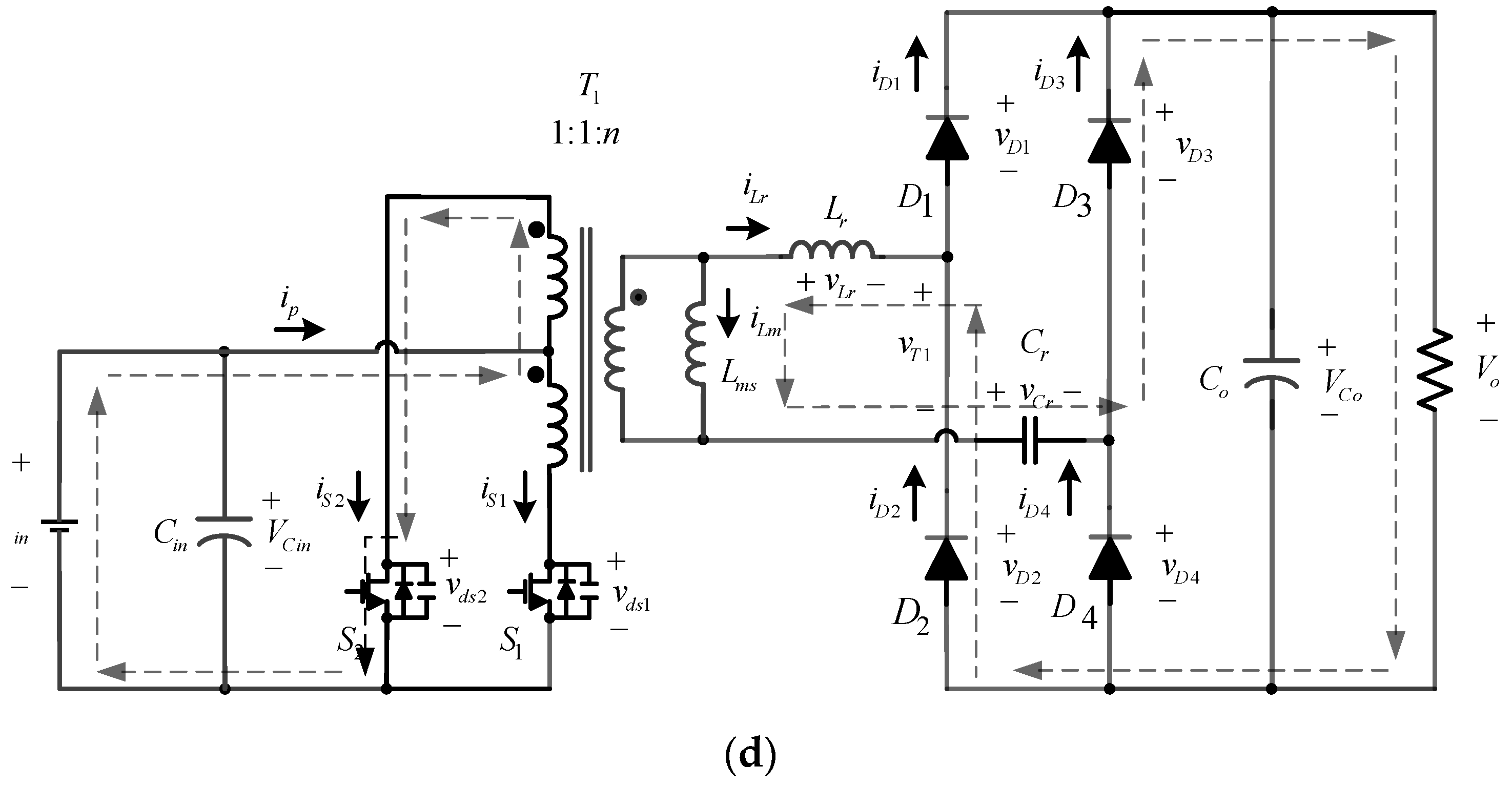
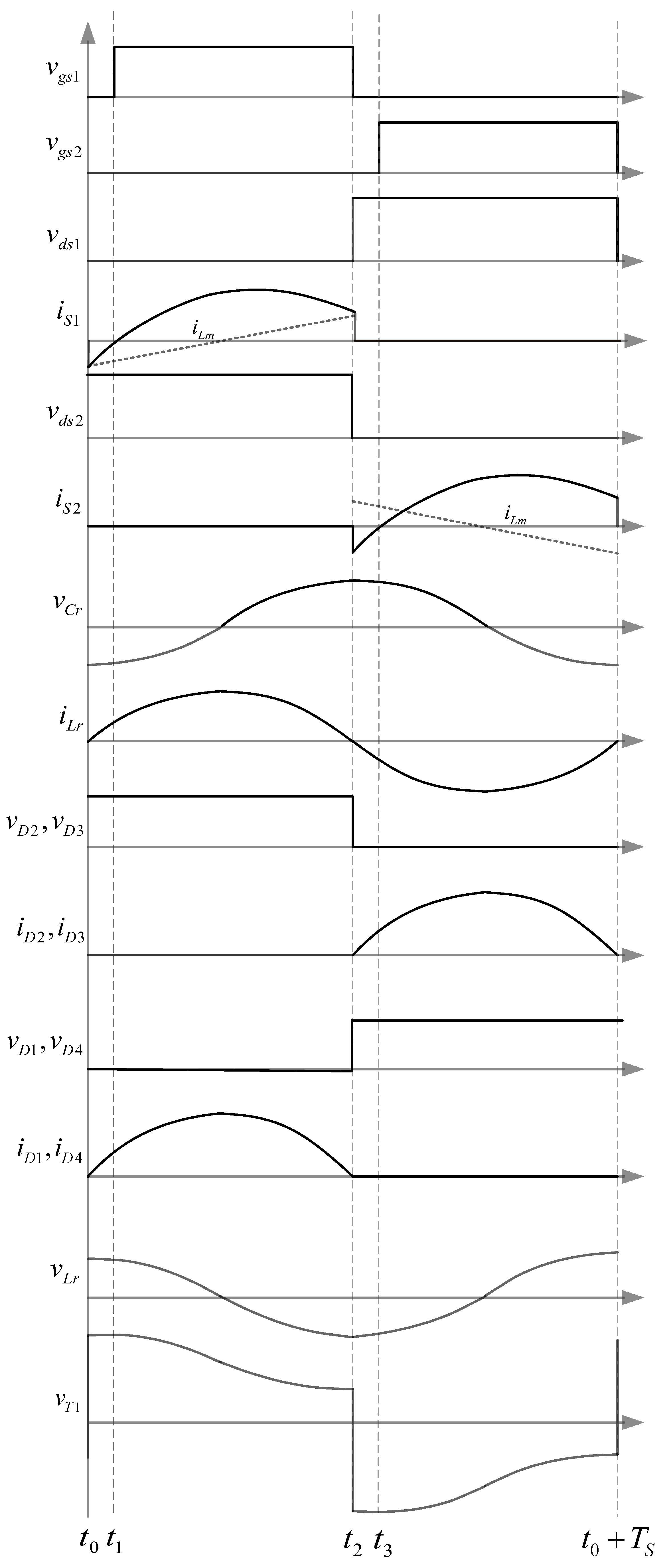
Finally, the switching frequency fs of the resonant converter is operated at the series resonant frequency fr, so that the resonant network is filtered at high frequency and rectified by the full-bridge rectifier to generate the DC output voltage. The proposed high gain set-up DC-DC converter is divided into four operating modes. Figure 7 and Figure 8 present the four operating modes and their theoretical waveforms, respectively.
Mode 1 [t0tt1]: This mode is shown in Figure 7a. During the dead time interval when the switch S2 is opened at time t0, the magnetizing current iLm of the secondary-side winding Ns quickly charges the drain-to-source capacitance across switch S2 to twice as high as the input voltage Vin. At the same time, the drain-to-source capacitance across switch S1 is discharged to zero and the body diode of the switch S1 is on. The magnetizing current iLm increases linearly as follows:
i L m ( t ) = i L m ( t 0 ) + ( n V i n ( t t 0 ) ) / L m s
According to (15), the peak value of the magnetizing current iLm depends on the input voltage Vin.
Mode 2 [t1tt2]: This mode is shown in Figure 7b. At time t1, the switch S1 is turned on at zero voltage, and the positive voltage of Vin is applied to the primary-side winding Np1 of the transformer. The duration of the switch is about half of switching the time interval. The power is transferred through the transformer to the secondary-side output DC link. The resonant inductance Lr and the resonant capacitor Cr produce resonance, and the current iLr flows through the diodes D1 and D4. Therefore, the corresponding equations of the voltage vCr across the resonant capacitor Cr, the voltage vLr across the resonant inductor Lr, and the current iLr in the resonant inductor Lr can be written as follows:
v C r ( t ) = v C r ( t 1 ) cos ω r ( t t 1 )
v L r ( t ) = ( n V i n V o ) v C r ( t 1 ) cos ω r ( t t 1 )
i L r ( t ) = ( n V i n V o v C r ) Z r sin ω r ( t t 1 )
On the primary side, the winding Np1 voltage of the transformer is Vin. Therefore, the drain-to-source voltage across switch S2 is twice as high as the input voltage Vin, while iLm still increases linearly. The equation of current is1 is as follows:
i s 1 = n ( i L r ( t ) + i L m ( t ) )
Mode 3 [t2tt3]: This mode is shown in Figure 7c; during the dead time interval when switch S1 is opened at t2, the converter operates similar to Mode 1. The magnetizing iLm of the secondary-side winding Ns quickly charges the drain-to-source capacitance across switch S1 to twice as high as the input voltage Vin. At the same time, the drain-to-source capacitance of the switch S2 is discharged to zero and the body diode of the switch S2. The magnetizing current iLm decreases linearly in reverse.
i L m ( t ) = i L m ( t 2 ) ( n V i n ( t t 2 ) ) / L m s
Mode 4 [t3tt0 + Ts]: This mode is shown in Figure 7d; at time t3, the switch S2 is turned on at zero voltage, and the positive voltage of Vin is applied to the primary-side winding Np2 of the transformer. The duration is about half of switching period the time interval. The power is transmitted through the transformer to the secondary-side output DC link. Both the resonant inductance Lr and the resonant capacitor Cr resonate, and the current iLr flows through the diodes D2 and D3. Therefore, the state equations of the voltage vCr across the resonant capacitor Cr, the voltage vLr across the resonant inductor Lr, and the current iLr in the resonant inductor Lr can be written as follows:
v C r ( t ) = v C r ( t 3 ) cos ( π + ω r ( t t 3 ) )
v L r ( t ) = ( n V i n V o ) v C r ( t 3 ) cos ( π + ω r ( t t 3 ) )
i L r ( t ) = ( n V i n V o v C r ) Z r sin ( π + ω r ( t t 3 ) )
The primary winding Np2 voltage of the transformer is Vin. Therefore, the drain-to-source voltage across the switch S1 is twice as high as Vin, while iLm still increases linearly in the opposite direction. The expression of current iS2 is as follows:
i s 2 = n ( i L r ( t ) + i L m ( t ) )
In following section, how to choose the suitable components used in this paper will be discussed.

4. Design Considerations

Here, a prototype with an input voltage of 43~52 V and an output voltage of 370~410 V and an output power of 500 W is proposed to verify the feasibility of this structure. The design procedure is divided into two parts. First, the primary-side switches and the turns ratio of the transformer are designed based on the push-pull converter structure. The second part designs the inductance and capacitance in the resonant tank of the secondary side based on the electrical parameters of the transformer. Finally, the final component parameter specifications are determined to complete a test prototype. The complete design process is described as follows:
(1)
To determine the turns ratio n
First, choose the maximum duty cycle Dmax = 0.46.
n = V o _ m i n 2   ×   V i n _ m i n   ×   D m a x     = 380 2   ×   43   ×   0.46 = 9.605
Finally, the turns ratio is chosen as 10.
(2)
To calculate the maximum voltage stress Vs_max of the drain source of the MOSFET switch
The maximum DC input voltage plus the peak voltage caused by the leakage inductance under the assumption of a peak voltage of 30% of Vin is selected for Vs_max.
V s _ m a x = 2 × 1.3 × V i n _ m a x              = 2 × 1.3 × 52 = 135.2   V
Finally, the MOSETs with withstand voltage greater than 135.2 V are chosen as switches.
(3)
To calculate the voltage stress across the output diode
The maximum reverse voltage stress across the diode is
V d _ m a x = n V i n _ m a x              = 10 × 52 = 520   V
Finally, the ultra-fast diodes with withstand voltage greater than 520 V are chosen as output didoes.
(4)
To design the secondary-side magnetizing inductance Lms
A complete power delivery operation is included in each half switching cycle, where the resonant half cycle is completed within the switching half cycle. At the end of the switching half cycle, the resonant inductor current iLr reaches the magnetizing current iLm, and the rectifier current reaches zero. For the resonant tank to have unity gain and best optimized operation and efficiency, the turns ratio of the transformer is designed such that the converter operates at resonance at nominal input voltage.
During the dead time of tdead, the voltage on the drain-to-source capacitor is discharged to zero to ensure zero voltage switching (ZVS). During this period, the magnetizing current is equal to the peak magnetization current, iLm,peak. Therefore, iLm and the corresponding equality can be expressed as
i L m = n V i n × T 4 L m
i L m , p e a k × t d e a d = 2 C e q × V i n
where Ts is the switch switching period equal to the resonance period Tr, Ceq is the equivalent output capacitance of the MOSFET, and the magnetizing inductance Lm should satisfy the following inequality:
L m < T s × t d e a d 8 C e q
(5)
To calculate values of resonant elements
The value of Lm can be estimated based on (30), considering the appropriate AC resistance value of Rac is shown in (31). In addition, the resonant frequency fr is equal to the switching frequency fs as 135 kHz, and a low Q value of 0.34 is selected to achieve a better boost gain value. Then, the values of Lr and Cr based on (32) and (33) can be obtained.
R a c = 8 π 2 V o I o = 8 3 . 14 2 × 380 1 . 25 = 246 . 6   Ω
C r = 1 2 π f r R a c Q       = 1 2 π   ×   135   ×   10 3   ×   246 . 6   ×   0 . 34 = 14 . 1   nF
L r = 1 ( 2 π f r ) 2 C r       = 1 ( 2 π   ×   135   ×   10 3 ) 2   ×   14.1   ×   10 9 = 100   μ H
The summary parameter design is shown in Table 1.
In following section, some simulation and experimental results are offered to demonstrate the feasibility and effectiveness of the proposed control strategy.

5. Simulation and Experimental Results

5.1. Simulation Rsults

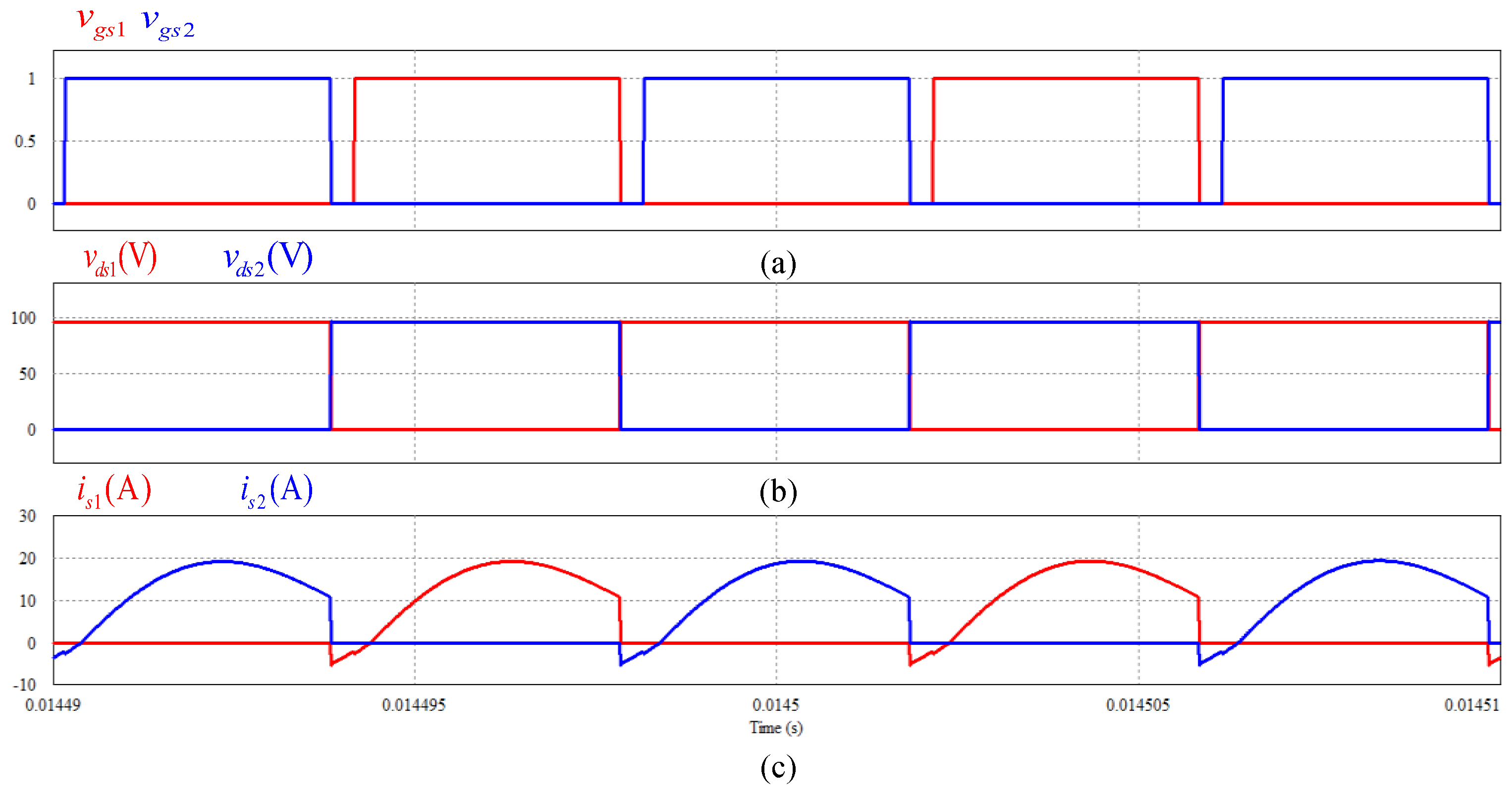
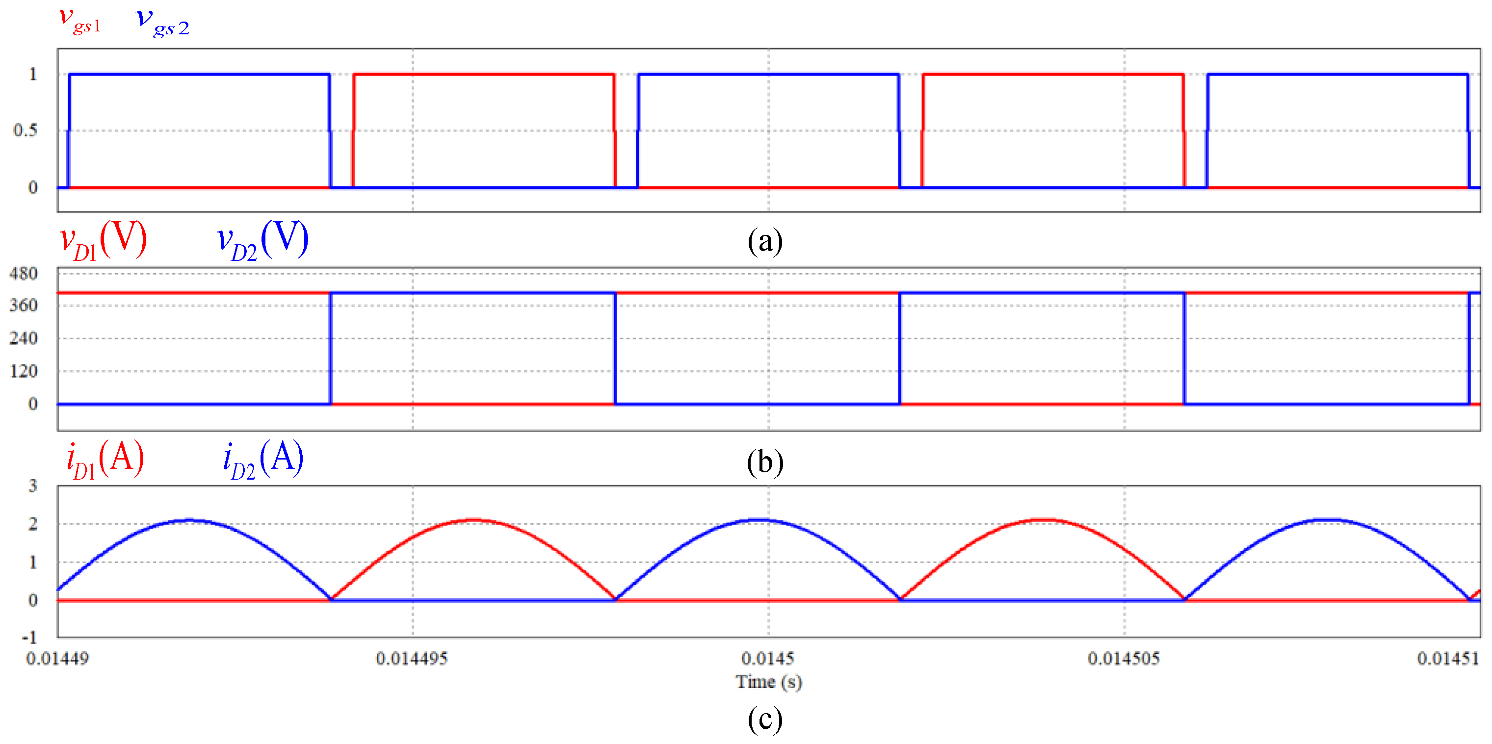
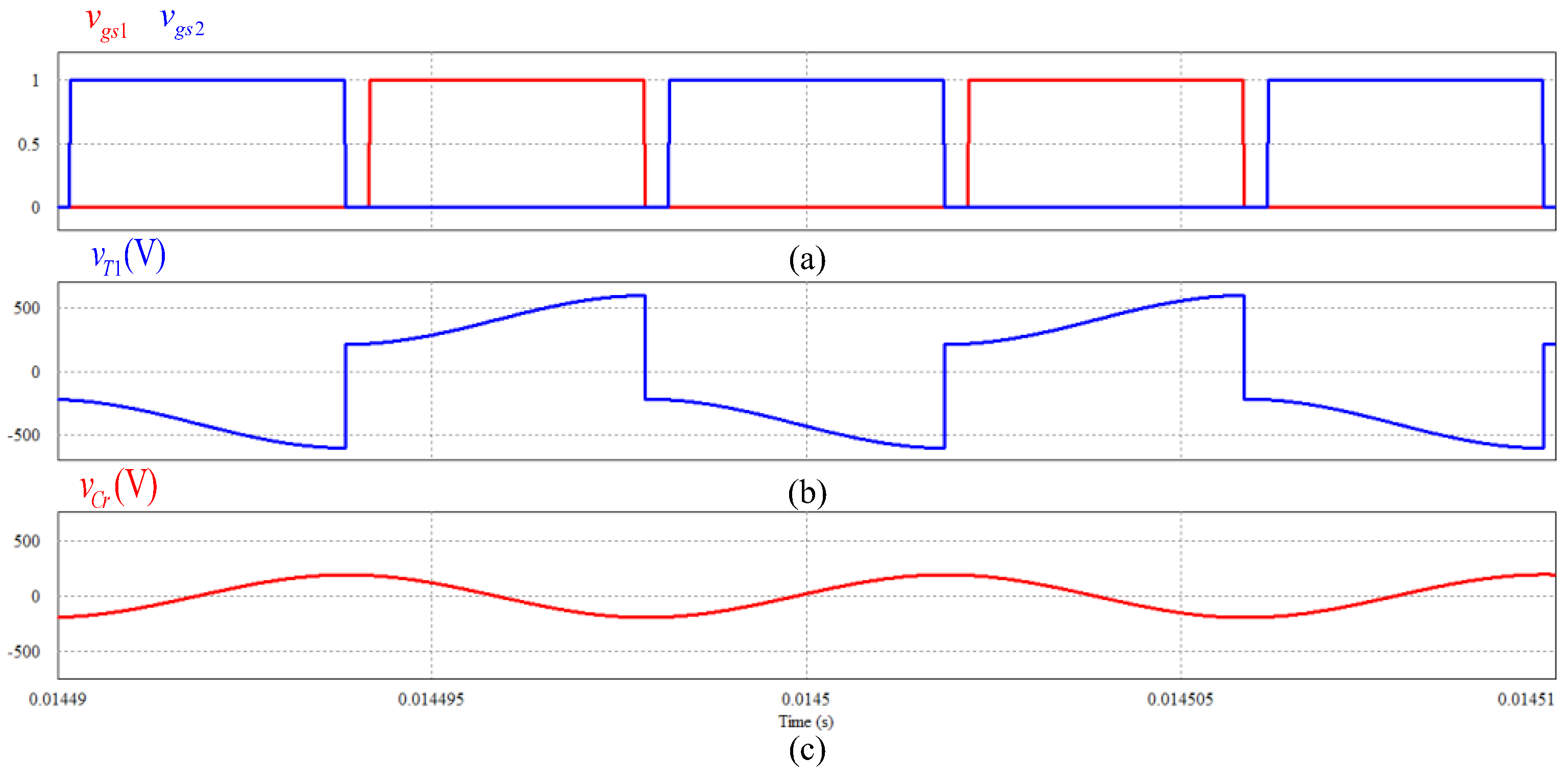
To verify the theoretical analysis of the proposed converter under steady-state conditions, the proposed converter is simulated using PSIM Ver. 9.1 according to the design described in Table 1 with a rated input voltage of 48 V and an output power of 500 W. Figure 9 shows the voltage and current waveforms of the primary-side switches. Figure 10 shows the voltage and current waveforms of the secondary-side rectifier diodes. Figure 11 shows the voltage vCr waveform of the resonant capacitor Cr, and the output voltage vT1 waveform of the transformer T1.
Figure 9 shows the voltage vds1, vds2 and current is1 and is2 waveforms of switch S1 and S2. It can be seen from this figure that before any switch is turned on, a negative current flows through the switch, so the switch is turned on with zero voltage switching (ZVS). Moreover, it indicates that the current in the switch is reduced by the resonance between Lr and Cr before the switch is turned off. Therefore, when the switch is off, the current stress through the switch can be minimized. Figure 10 shows the voltages vD1, vD2, and currents iD1 and iD2 waveforms of the full-bridge rectifier diodes. From this figure, it can be seen that the current in the diodes are turned off when they decrease to zero. As a result, the diodes are turned off at zero current and reverse recovery losses are eliminated. As can be seen from Figure 11, the transformer output voltage vT1 and the voltage vCr of the resonant capacitor show that the sum of vT1 and vCr becomes negative and positive DC voltages alternately. The current iLr of the resonant inductor is a sinusoidal output, which means that the input current of the full-bridge rectifier is a sinusoidal wave.

5.2. Experimental Results

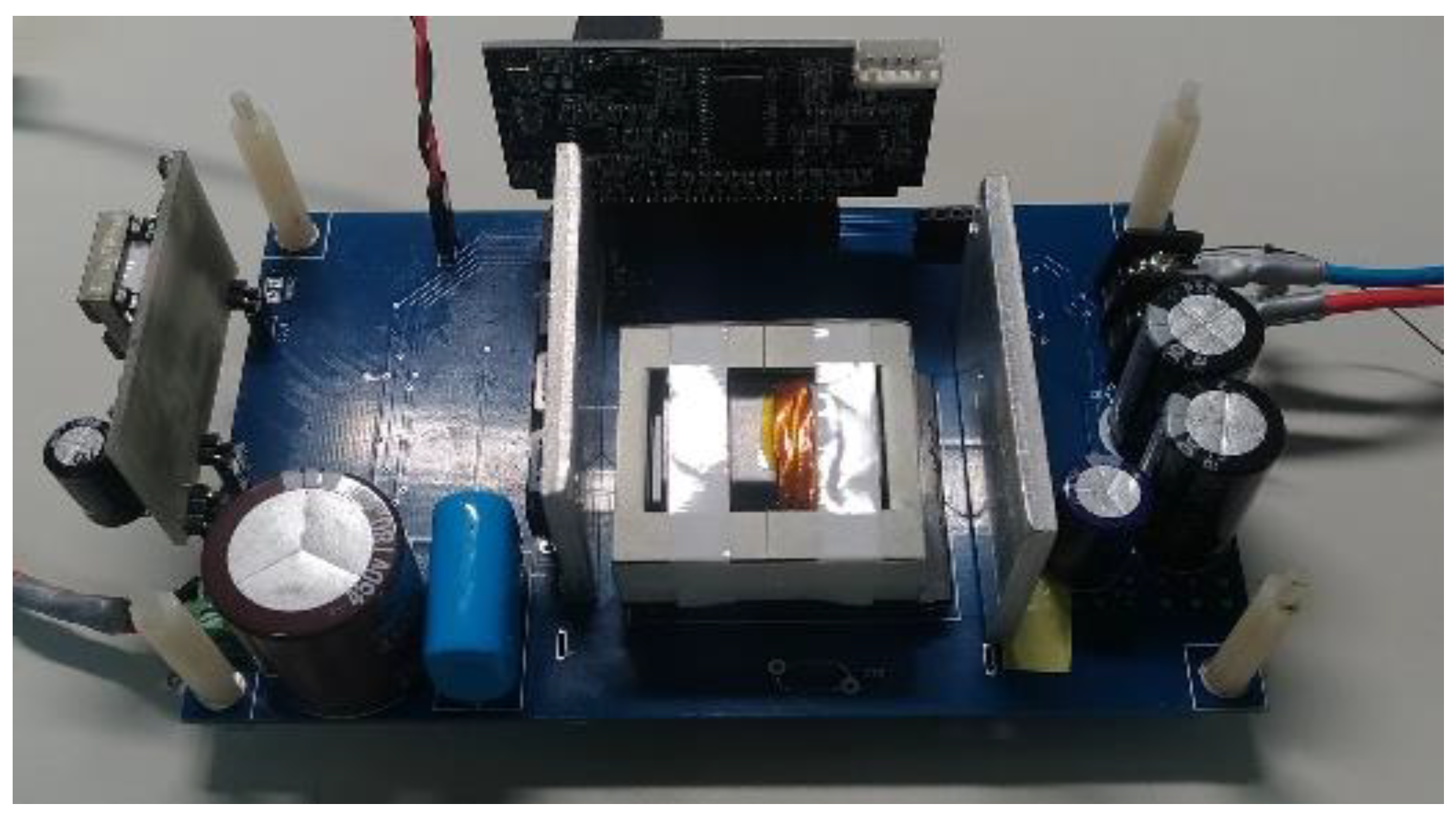
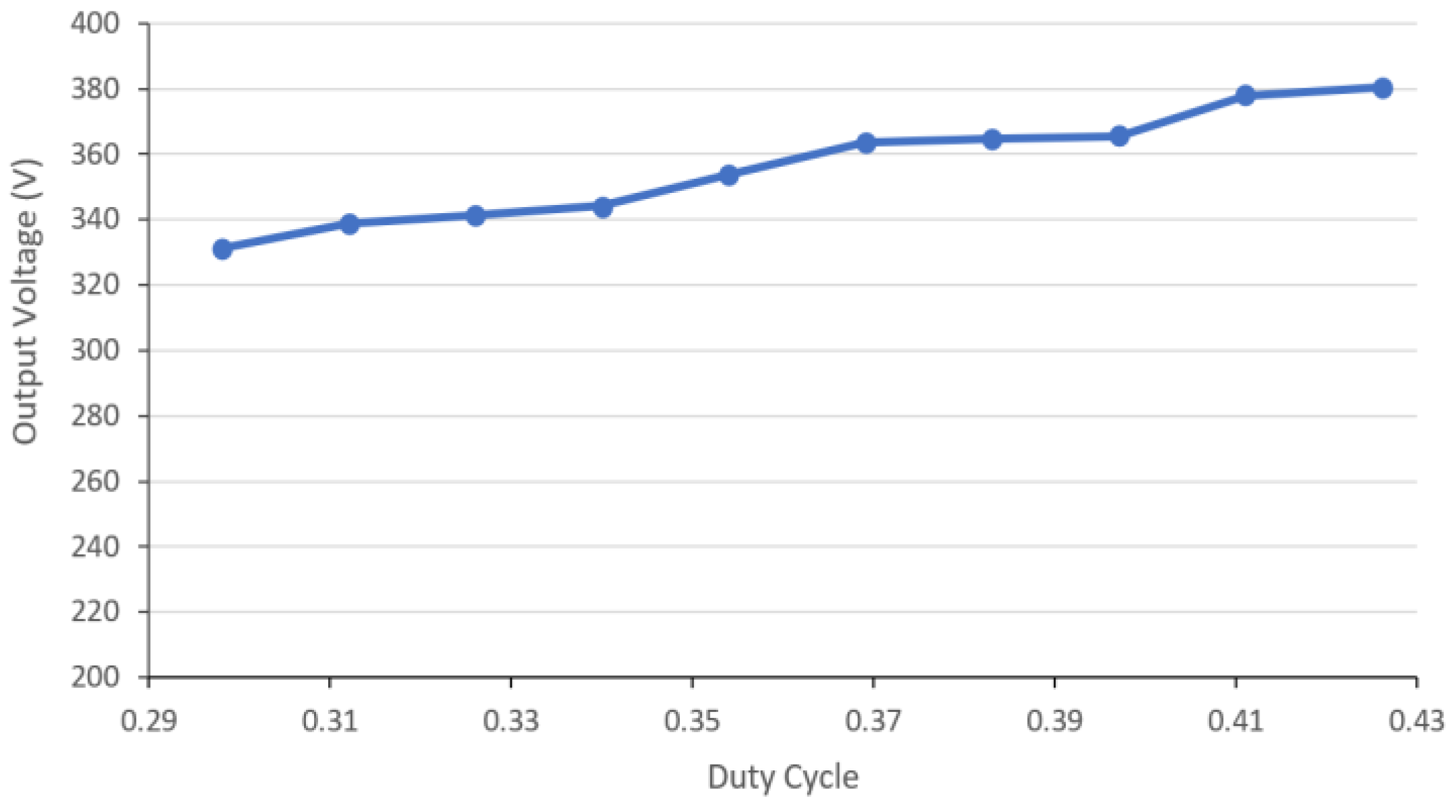
According to the structure of the protype, a 500 W prototype has input voltage range from 43 V to 52 V. A photo of the prototype is shown in Figure 12. The proposed converter will be used in the backup power supply of the green energy industry. For the storage battery pack to be considered, it should avoid depth of discharge (DOD), reducing battery pack charging and discharging cycles. In order to extend the service life of the battery, the voltage of the low-voltage side of the proposed structure is used to simulate the 48 V battery pack which takes constant current discharge. To speak lucidly, the output voltage of this battery pack can be represented as battery capacity to some extent. Under this condition, the proposed converter is controlled at a given constant current according to the battery voltage. As the terminal voltage of the battery locates between 44 V and 45 V, it is discharged with a constant current of 2 A, whereas as the terminal voltage of the battery locates between 46 V and 52 V, it is discharged with a constant current of 10.5 A. As the voltage falls below 43 V, discharge is terminated to avoid deep discharge. In addition, the high voltage output of the converter is controlled by the next-stage inverter to keep the output voltage at some output voltage range and this will be implemented in the future. In addition, Figure 13 shows a curve of output voltage versus duty cycle.
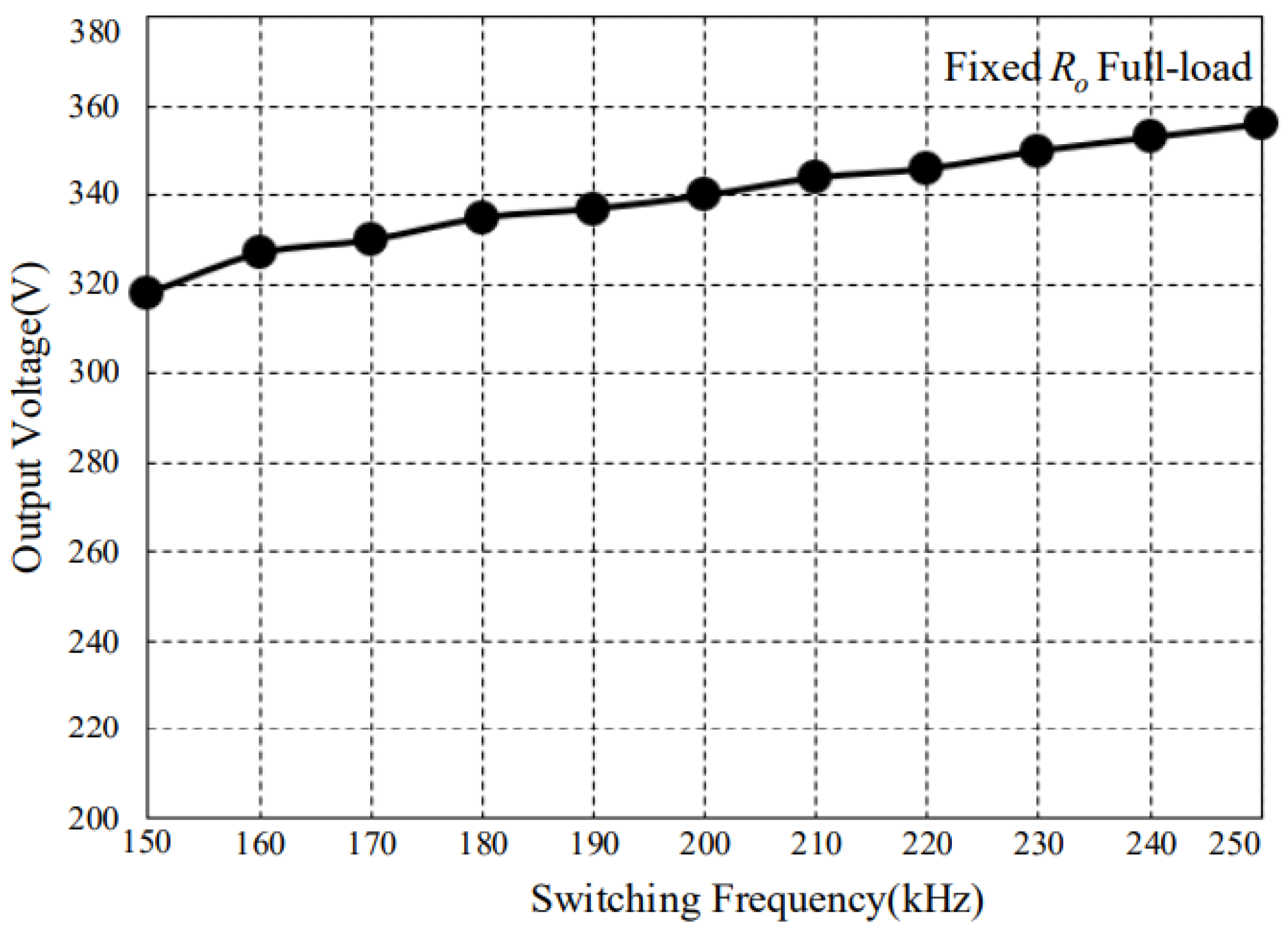
Sequentially, the following description focuses on the fact that the proposed control strategy has a better adjustable output voltage. According to Figure 14 coming from [23], the output voltage is increased from 320 V to 360 V with the corresponding frequency from 150 kHz to 250 kHz at a fixed load. The results of the proposed control strategy are shown in Figure 13. Under a fixed input voltage and output load, the output voltage is increased from 330 V to 380 V with the corresponding duty cycle from 0.3 to 0.42. The former has a regulated voltage range of 40 V (= 360 V − 320 V) with a regulation ratio of 0.4 [= (250 kHz − 150 kHz)/250 kHz)], whereas the latter has a regulated voltage range is 50 V (= 380 V − 330 V) with a regulated ratio of 0.12 [= (0.42 − 0.3)/0.42]. That is to say, based on these calculations, the latter with the proposed control strategy has a better adjustable output voltage range.
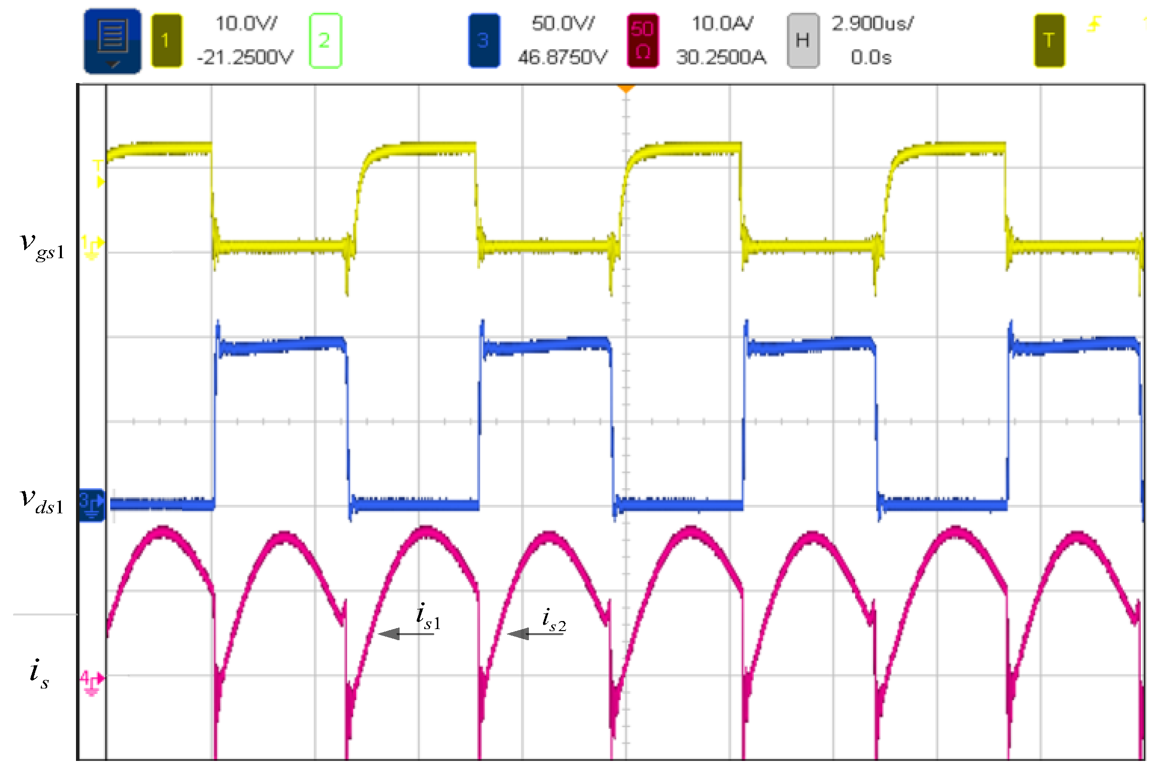
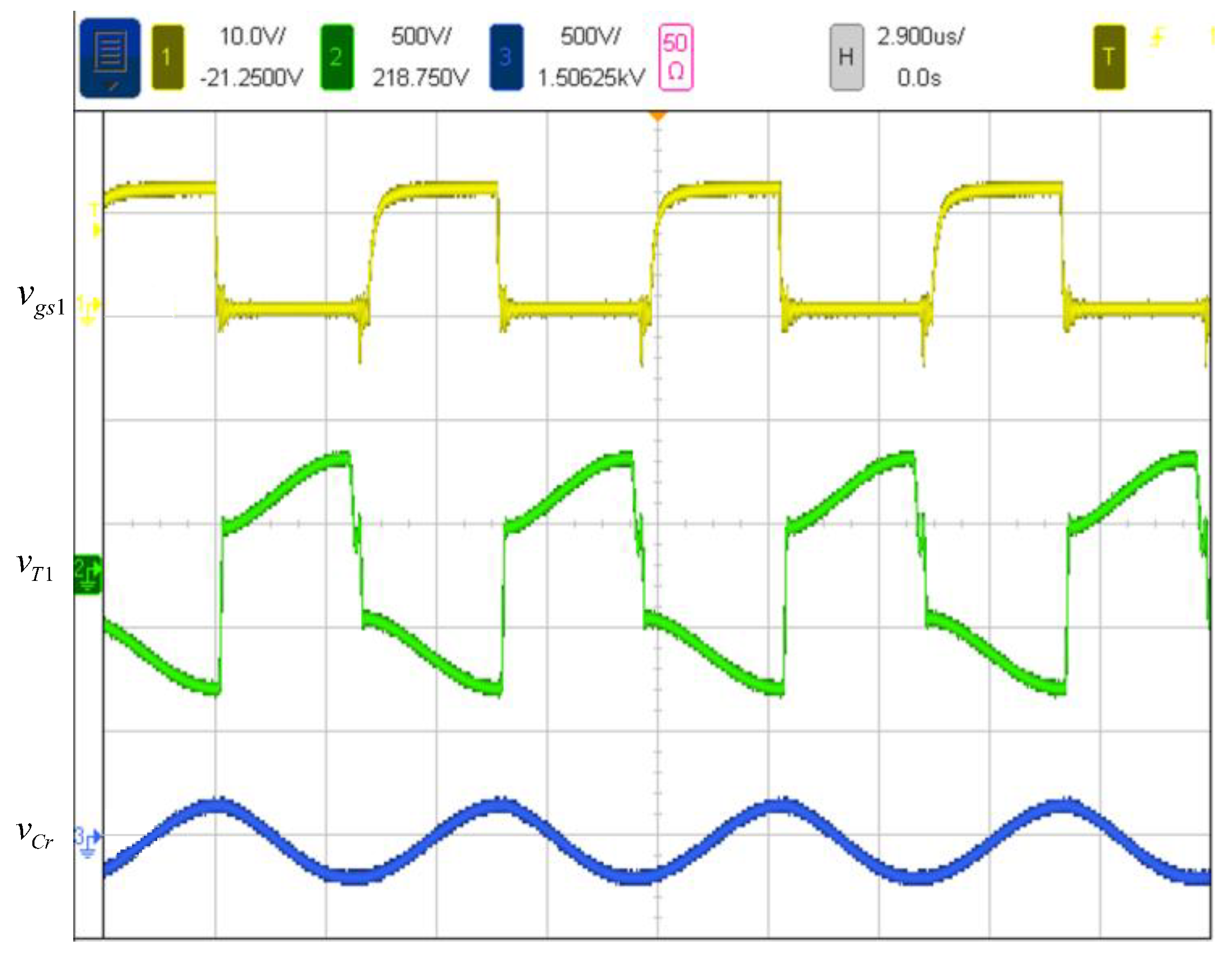
In order to demonstrate the performance of the proposed converter, Figure 15, Figure 16 and Figure 17 show the experimental waveforms of the prototype. Figure 15 shows the waveforms of the drain-to-source voltages vds1 and drain-to-source current iS1 of the switch S1. Via soft switching, the switch is turned off when the drain-to-source current iS is minimum to some extent, and the switch is turned on with ZVS when the voltage on the drain-to-source vds is discharged to zero. Figure 16 shows the measured waveforms of the reverse voltage vD3 and output current iD of the full-bridge rectifier diodes D1, D2, D3 and D4. Before the diode D3 is reversed, the diode current iD3 reaches zero, and hence the diode is turned off with ZCS. Moreover, the reverse recovery problem of the diodes is also alleviated, and hence the reverse recovery loss is eliminated. Figure 17 shows the output voltage vT1 and the voltage vCr of the resonant capacitor. In this figure, the resonant inductor is embedded in the transformer, so the output voltage of the transformer is the output voltage of the resonant circuit superimposed on the voltage vLr of the resonant inductor. From Figure 17, it can be seen that the sum of the transformer output voltage vT1 and the voltage vCr of the resonant capacitor becomes negative and positive DC voltages alternately. The output current of the transformer is filtered by the resonant circuit and becomes a sinusoidal current outputted to the full-bridge rectifier.
The experimental results of the prototype under different input voltages and different constant current loads are shown in Table 2.
The efficiency is 90.2% at Vin of 43 V and load of 45 W. The efficiency is 96.9% at Vin of 46 V and load of 468 W. The maximum efficiency is 97.1% at Vin of 50 V and load of 510 W.
Table 3 provides a comparison of the characteristics of the proposed converter with similar circuit structures in recent years. The proposed converter is suitable for high set-up applications, achieving higher voltage gain with less total components count and higher efficiency through power-optimized design.
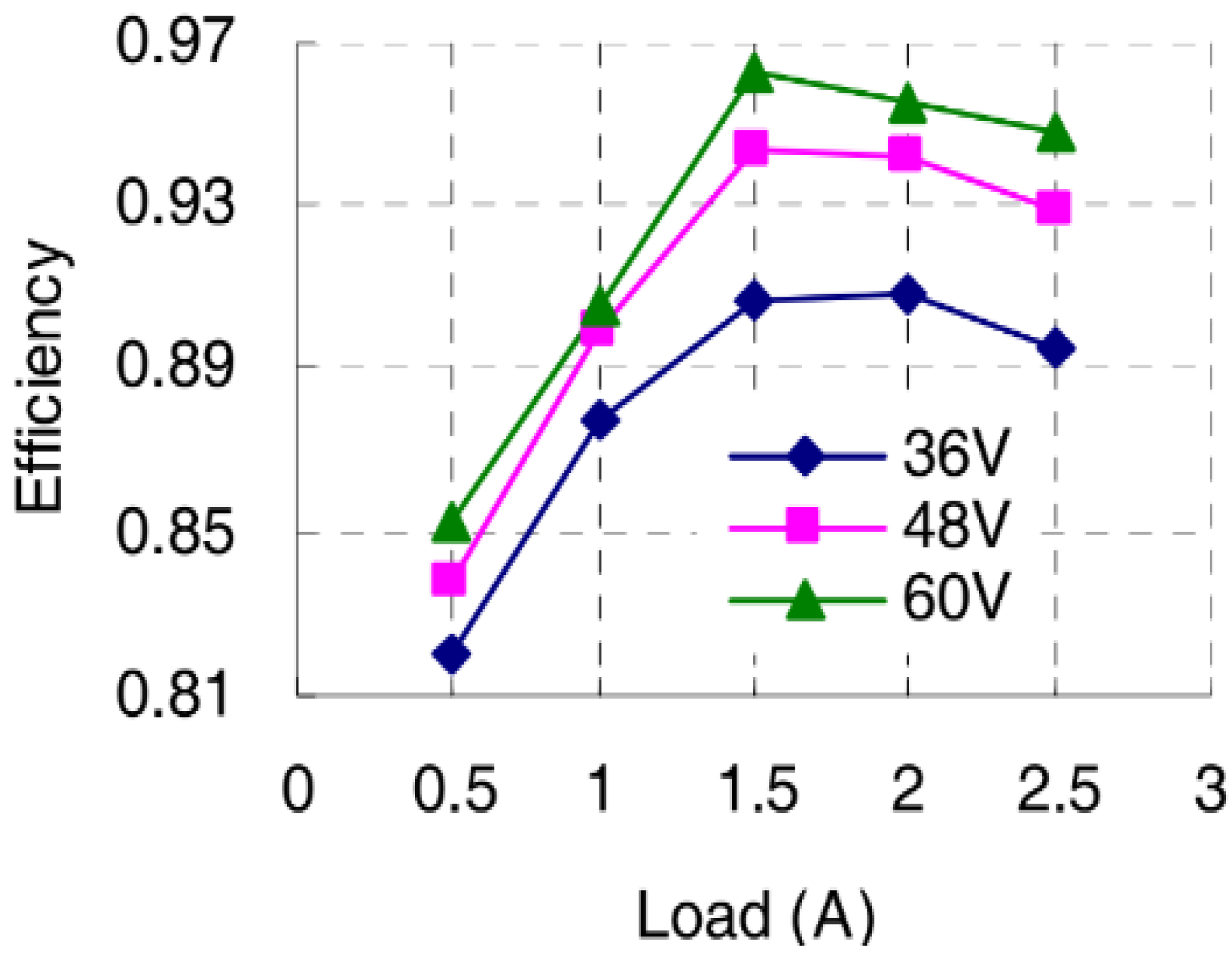
Afterwards, the following description focuses on the fact that the proposed structure and control strategy has better efficiency. According to Figure 18 coming from [24], the curve of efficiency versus input voltage and load shows that the efficiency is about 0.82 at input voltage of 36 V and 20% load, the efficiency is about 0.84 at input voltage of 48 V and 20% load, the efficiency is about 0.85 at input voltage of 60 V and 20% load, and the efficiency is about 0.95 at input voltage of 60 V and rated load. As described in Table 2 of the proposed structure and control strategy, the efficiency is 0.902 at input voltage of 43 V and 9% load, and the efficiency 0.971 at input voltage of 50 V is about rated load. Based on the above comparison, it can be seen that the proposed structure and control strategy can improve the efficiency, particularly for light load.

6. Conclusions

This paper proposes ZVS/ZCS push-pull DC/DC converters, which can be applied to backup power systems, such as online uninterruptible power supply (UPS), smart residential power systems and battery energy storage systems in energy storage applications. They can be used as an alternative design for 48 V battery systems, and provide higher power density, reduced weight and size, low cost and high scalability. An LC resonant circuit is constructed by using the secondary-side leakage inductance of the transformer and the series resonant capacitor to realize zero voltage switching (ZVS) of the primary-side switches and zero current switching (ZCS) of the secondary-side diodes to reduce switching losses. As a result, all the switching components have soft switching that reduces switching losses and allows higher frequency switching operations to achieve more compact converters and higher power density. The proposed control method is simple and easy to implement to the high-voltage DC bus for higher power applications.

Author Contributions

Conceptualization, Y.-K.T. and K.-I.H.; methodology, Y.-K.T. and K.-I.H.; software, Y.-K.T.; validation, Y.-K.T. and K.-I.H.; formal analysis, Y.-K.T. and K.-I.H.; investigation, Y.-K.T.; resources, Y.-K.T.; data curation, Y.-K.T.; writing—original draft preparation, Y.-K.T. and K.-I.H.; writing—review and editing, K.-I.H.; visualization, Y.-K.T.; supervision, K.-I.H.; project administration, K.-I.H.; funding acquisition, K.-I.H. All authors have read and agreed to the published version of the manuscript.

Funding

This research was funded by the Ministry of Science and Technology, Taiwan, under the Grant Number: MOST 110-2221-E-027-045-MY2.

Data Availability Statement

No new data were created or analyzed in this study. Data sharing is not applicable to this article.

Conflicts of Interest

The authors declare no conflict of interest.

References

  1. Mohtasham, J. Review Article-Renewable Energies. Energy Procedia 2015, 74, 1289–1297. [Google Scholar] [CrossRef] [Green Version]
  2. Lawder, M.T.; Suthar, B.; Northrop, P.W.C.; De, S.; Hoff, C.M.; Leitermann, O.; Crow, M.L.; Santhanagopalan, S.; Subramanian, V.R. Battery Energy Storage System (BESS) and Battery Management System (BMS) for Grid-Scale Applications. Proc. IEEE 2014, 102, 1014–1030. [Google Scholar] [CrossRef]
  3. Lowder, T.; Xu, K. The Evolving U.S. Distribution System: Technologies, Architectures, and Regulations for Realizing a Transactive Energy Marketplace; Technical Report; National Renewable Energy Laboratory: Golden, CO, USA, 2020. [Google Scholar]
  4. Mumtaz, F.; Yahaya, N.Z.; Meraj, S.T.; Singh, B.; Kannan, R.; Ibrahim, O. Review on non-isolated DC-DC converters and their control techniques for renewable energy applications. Ain Shams Eng. J. 2021, 12, 3747–3763. [Google Scholar] [CrossRef]
  5. Hossain, M.Z.; Selvaraj, J.A.L.; Rahim, N.A. High voltage-gain full-bridge cascaded dc-dc converter for photovoltaic application. Public Library of Science: San Francisco, CA, USA, 2018.
  6. Tomaszuk, A.; Krupa, A. High efficiency high step-up DC/DC converters-a review. Bull. Pol. Acad. Sci. Tech. 2011, 59, 475–483. [Google Scholar] [CrossRef] [Green Version]
  7. Padhee, S.; Pati, U.C.; Mahapatra, K. Overview of high-step-up DC–DC converters for renewable energy sources. IETE Tech. Rev. 2018, 35, 99–115. [Google Scholar] [CrossRef]
  8. Sreelekha, S.; Vivek, P.V.; Anupama, P.K. A high step up DC-DC converter using isolated coupled inductor. Int. Res. J. Eng. Technol. 2020, 7, 6989–6993. [Google Scholar]
  9. Swaminathan, N.; Lakshminarasamma, N.; Cao, Y. DCM and CCM operation of buck-boost full-bridge DC-DC converter. In Proceedings of the IEEE Applied Power Electronics Conference and Exposition, Phoenix, AZ, USA, 14–17 June 2021; pp. 292–297. [Google Scholar]
  10. Wei, Y.; Luo, Q.; Mantooth, A. A hybrid half-bridge LLC resonant converter and phase shifted full-bridge converter for high step-up application. In Proceedings of the IEEE Workshop on Wide Bandgap Power Devices and Applications in Asia, Suita, Japan, 23–25 September 2020; pp. 1–6. [Google Scholar]
  11. Anand, M.; Rahul, P.P.; Eldhose, K.P.; Alex, L.T. Design of interleaved push pull converter for photovoltaic systems. IOSR J. Eng. 2018, 1, 73–80. [Google Scholar]
  12. Ying, J.; Zhu, Q.; Lin, H.; Wu, Z. A zero-voltage-switching (ZVS) push-pull DC/DC converter for UPS. In Proceedings of the The Fifth International Conference on Power Electronics and Drive Systems, Singapore, 17–20 November 2003; pp. 1495–1499. [Google Scholar]
  13. Veeresh, H.; Ashok, K. ZCS/ZVS push pull DC/DC converter. Int. J. Latest Technol. Eng. 2015, 4, 73–79. [Google Scholar]
  14. Jafari, A.; Matioli, E. High step-up high-frequency zero-voltage switched GaN-based single-stage isolated DC-DC converter for PV integration and future DC grids. In Proceedings of the PCIM Europe, Nuremberg, Germany, 5–7 June 2018; pp. 325–330. [Google Scholar]
  15. Sha, D.; Luo, T. A novel push-pull forward converter with a passive resonant network introduced in the secondary winding. In Proceedings of the IEEE Applied Power Elctronics Conference and Exposition, Fort Worth, TX, USA, 16–20 March 2014; pp. 2081–2086. [Google Scholar]
  16. Wu, T.F.; Hung, J.C.; Tsai, J.T.; Tsai, C.T.; Chen, Y.M. An active-clamp push-pull converter for battery sourcing applications. IEEE Trans. Ind. Appl. 2008, 44, 196–204. [Google Scholar] [CrossRef]
  17. Wu, Q.; Wang, Q.; Xu, J.; Xu, Z. Active-clamped ZVS current-fed push–pull isolated dc/dc converter for renewable energy conversion applications. IET Power Electron. 2018, 11, 373–381. [Google Scholar] [CrossRef]
  18. Tandon, S.; Rathore, A.K. Analysis and design of series LC partial-resonance-pulse-based ZCS current-fed push-pull converter. IEEE Trans. Ind. Appl. 2021, 57, 4234–4241. [Google Scholar] [CrossRef]
  19. Yuan, Y.; Chang, L.; Song, P. A new LCL-resonant push-pull DC-DC converter for inverter applications. In Proceedings of the Large Engineering Systems Conference on Power Engineering, Montreal, QC, Canada, 10–12 October 2007; pp. 261–264. [Google Scholar]
  20. Sam, A.R. Resonant LLC Converter: Operation and Design; Infineon Technologies, Application Note, AN 2012-09, V1.0; Infineon Technologies North America (IFNA) Corp: Durham, NC, USA, 2012. [Google Scholar]
  21. Boonyaroonate, I.; Mori, S. A new ZVCS resonant push-pull DC/DC converter topology. In Proceedings of the Seventeenth Annual IEEE Applied Power Electronics Conference and Exposition, Dallas, TX, USA, 10–14 March 2002; pp. 1097–1100. [Google Scholar]
  22. Bilsalam, A.; Jinati, T.; Wongphasuk, W.; Ekkaravarodome, C.; Chunkag, V. High step-up push-pull resonant converter based on current source class-D rectifier. In Proceedings of the International Conference on Electrical Engineering/Electronics, Computer, Telecommunications and Information Technology, Prachuap Khiri Khan, Thailand, 24–27 May 2019; pp. 533–536. [Google Scholar]
  23. Bilsalam, A.; Ekkaravarodome, C.; Chunkag, V.; Thounthong, P. Analyzing the effect of parasitic capacitance in a full-bridge Class-D current source rectifier on a high step-up push-pull multiresonant converter. Sustainability 2021, 13, 5477. [Google Scholar] [CrossRef]
  24. Chen, W.; Lu, Z.; Zhang, X.; Ye, S. A novel ZVS step-up push-pull type isolated LLC series resonant dc-dc converter for UPS systems and its topology variations. In Proceedings of the Twenty-Third Annual IEEE Applied Power Electronics Conference and Exposition, Austin, TX, USA, 24-28 February 2008; pp. 1073–1078. [Google Scholar]
  25. Rahman, A.N.; Chiu, H.J.; Hsieh, Y.C. Design of wide input voltage range high step-up DC-DC converter based on secondary-side resonant tank full bridge LLC. In Proceedings of the 3rd International Conference on Intelligent Green Building and Smart Grid (IGBSG), Yilan, Taiwan, 22–25 April 2018; pp. 1–6. [Google Scholar]
  26. Liu, F.; Wan, J.; Jiang, L.; Li, Y.; Liu, K.-Z. A new soft-switching AC-DC converter based on coupled inductors for onboard charging applications. IEEE Trans. Power Electron. 2023, 38, 3433–3443. [Google Scholar] [CrossRef]
  27. Wang, S.; Zhou, C.; Riaz, S.; Guo, X.; Zaman, H.; Mohammad, A.; Al-Ahmadi, A.A.; Alharbi, Y.M.; Ullah, N. Adaptive fuzzy-based stability control and series impedance correction for the grid-tied inverter. Math. Biosci. Eng. 2023, 20, 1599–1616. [Google Scholar] [CrossRef] [PubMed]
  28. Li, J.; Riaz, S.; Zaman, H.; Hao, P.; Luo, Y.; Mohammad, A.; Al-Ahmadi, A.A.; Ullah, N. Duplex PD inertial damping control paradigm for active power decoupling of grid-tied virtual synchronous generator. Math. Biosci. Eng. 2022, 19, 12031–12057. [Google Scholar]
  29. Ye, M.Y.; Song, P.G.; Li, S.; Xiao, Y.H. Voltage-fed push-Pull PWM converter featuring wide ZVS range and Low circulating loss with simple auxiliary circuit. J. Power Electron. 2018, 18, 965–974. [Google Scholar]
  30. Wu, Q.; Wang, Q.; Xu, J.; Li, H.; Xiao, L. A high-efficiency step-up current-fed push-pull quasi-resonant converter with fewer components for fuel cell application. IEEE Trans. Ind. Electron. 2017, 64, 6639–6648. [Google Scholar] [CrossRef]
  31. Jia, P.; Yuan, Y. Analysis and design of an isolated high stepup converter based on the secondary side quasi-resonant loops. IET Power Electron. 2020, 13, 1129–1143. [Google Scholar] [CrossRef]
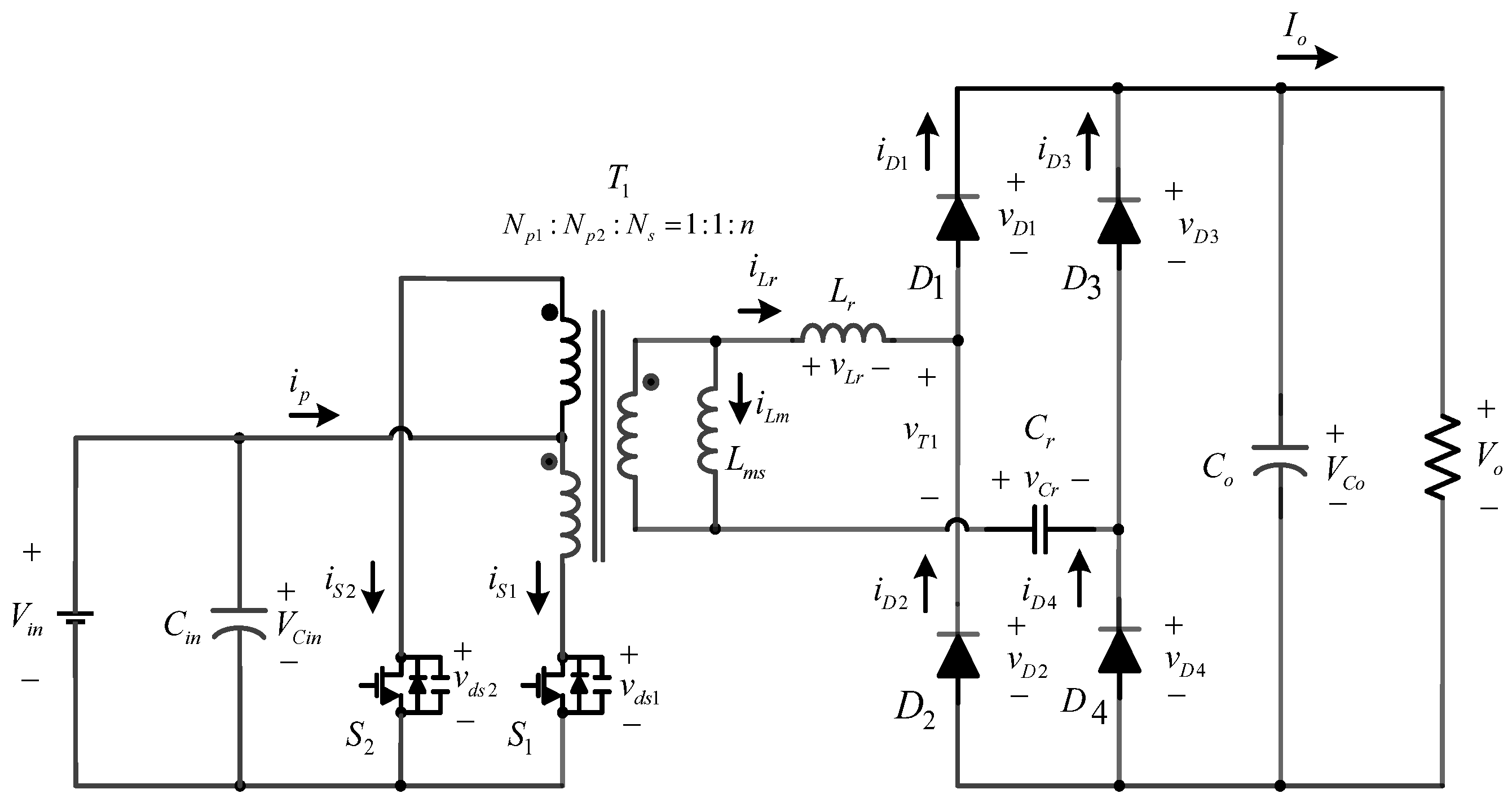
Figure 1. Proposed step-up DC-DC converter.
Energies 16 02892 g001
Figure 2. Equivalent circuit model of the center-tapped transformer.
Energies 16 02892 g002
Figure 3. Impedance diagram of the SRC.
Energies 16 02892 g003
Figure 4. Equivalent circuit of the proposed converter.
Energies 16 02892 g004
Figure 5. Relationship between characteristic impedance ||Zr|| and phase angle θZr and switching frequency fs.
Energies 16 02892 g005
Figure 6. Relationship between the ratio of vo to nvin under the normalized radian frequency with Q taken into account.
Energies 16 02892 g006
Figure 7. Operating modes of the proposed circuit: (a) Mode 1; (b) Mode 2; (c) Mode 3; (d) Mode 4.
Energies 16 02892 g007aEnergies 16 02892 g007b
Figure 8. Waveforms of the proposed circuit relevant to operating modes.
Energies 16 02892 g008
Figure 9. Simulation waveforms: (a) switch control signals vgs1 and vgs2; (b) switch drain-to-source voltages vds1 and vds2; (c) switch drain-to-source currents is1 and is2.
Energies 16 02892 g009
Figure 10. Simulation waveforms: (a) switch control signals vgs1 and vgs2; (b) output diode reverse voltages vD1 and vD2; (c) output diode reverse currents iD1 and iD2.
Energies 16 02892 g010
Figure 11. Simulation waveforms: (a) switch control signals vgs1 and vgs2; (b) secondary-side output voltage vT1; (c) resonant capacitor voltage vCr.
Energies 16 02892 g011
Figure 12. Experimental setup of a 500 W prototype.
Energies 16 02892 g012
Figure 13. Curve of output voltage versus duty cycle.
Energies 16 02892 g013
Figure 14. Relationship between output voltage Vo and varying frequencies fs [23].
Energies 16 02892 g014
Figure 15. Measurement waveforms: (1) switch control signal vgs1; (2) switch drain-source voltage vds1; (3) switch drain-source current iS1.
Energies 16 02892 g015
Figure 16. Measurement waveform: (1) switch control signal vgs1; (2) output diode reverse voltage vD3; (3) output diode forward currents iD1, iD4 and iD2, iD3.
Energies 16 02892 g016
Figure 17. Measurement waveforms: (1) switch control signal vgs1; (2) resonant-inductor-embedded transformer output voltage vT1; (3) the voltage vCr of the resonant capacitor.
Energies 16 02892 g017
Figure 18. Measured efficiency at different loads under all inputs [24].
Energies 16 02892 g018
Table 1. Main circuit specifications and component parameter specifications.
ParameterSymbolSpecification
Input voltageVin43~52 V
Output voltageVo370~410 V
Output powerPo100~500 W
Switching frequencyfs135 kHz
Duty cycle D0.42~0.46
Transformer turns ratioNp1:Np2:Ns4:4:40
Magnetizing inductanceLms720 µH
Leakage inductanceLlk (Lr)100 µH
Resonant capacitanceCr14.1 nF
Transformer coreT1PC40 (LP2930)
Primary-side switchesS1, S2IPP200N15N3G
Secondary-side diodesD1, D2, D3, D4BYV29X-600
Table 2. Measured efficiency of the prototype.
Input voltage Vin (V)434446485052
Input curent Iin (A)1.16210.510.510.510.5
Output voltage Vo (V)380380381398415421
Output power Wo (W)4584468489510527
Efficiency η90.2%95.5%96.9%97.0%97.1%96.5%
Table 3. Comparison of similar DC-DC converters.
Parameter[18][24][29][30][31]Proposed
Input voltage42–48 V36–60 V45–56 V30–50 V34–4043–52 V
Output voltage380 V240 V200 V350 V380 V370–410 V
Output power500 W600 W500 W510 W400 W520 W
Max. efficiency96.5%96.2%93.02%96.12%96.1%97.1%
Control techniqueVariable
frequency
Variable
frequency
Variable
duty cycle
Variable
duty cycle
Variable
frequency
Variable
duty cycle
No. of main switches223322
No. of diodes246264
No. of inductors/
transformers/
capacitors
1/1/32/1/11/1/21/1/31/1/40/1/1
Disclaimer/Publisher’s Note: The statements, opinions and data contained in all publications are solely those of the individual author(s) and contributor(s) and not of MDPI and/or the editor(s). MDPI and/or the editor(s) disclaim responsibility for any injury to people or property resulting from any ideas, methods, instructions or products referred to in the content.