Article

A Self-Powered FBRJT AC-DC Conversion Circuit for Piezoelectric Energy Harvesting Systems

1
Faculty of Engineering and Science, Southern Cross University, Lismore, NSW 2480, Australia
2
Department of Research and Development, MYRA Corporate, Wollongbar Industrial Area, Alstonville, NSW 2477, Australia
3
Department of Electronics and Control Engineering, National Institute of Technology, Niihama College, Ehime 792-0022, Japan
4
Faculty of Engineering and Science, Southern Cross University, Gold Coast, QLD 4225, Australia
*
Author to whom correspondence should be addressed.
Energies 2023, 16(4), 1734; https://doi.org/10.3390/en16041734
Submission received: 8 December 2022 / Revised: 26 January 2023 / Accepted: 7 February 2023 / Published: 9 February 2023

Abstract

:
In this study, a complete model for a miniature excitation-powered piezoelectric generator (PG), analysis modes of operation and control of a full-bridge joule thief (FBRJT) circuit to identify the optimal points were investigated. The proposed model revealed the PG’s power dependency on mechanical excitation, acceleration, and frequency and defined the load behaviour for power optimisation. The proposed circuit, namely FBRJT, was integrated with the conventional full-bridge rectifier (FBR) in Stage 1 for AC-DC conversion and with the joule thief circuit in Stage 2 for DC-DC conversion. This integration acted as a boost converter without utilising the duty cycles and additional switching components. The electrical nature of the input of FBRJT with a simple structure, sensor-less control and auxiliary circuits showed a consistent agreement with the investigated testing scenarios using both ideal and impedance power sources. Additionally, the performance of the proposed circuit was also verified against the published results of power electronics circuits. The developed versatile circuit and control system can be utilised for many applications, such as mobile battery charging and energy harvesting.

1. Introduction

Piezo generator (PG) is an emerging device that converts mechanical energy (ME), i.e., vibration existing in the environment, into electrical energy (EE), i.e., alternating current (AC). Over the last decade, there has been a growing emphasis among the scientific community on piezoelectric energy harvesting (PEH) systems. However, in real life, PGs are restricted to low power domains within the range of micro/milliwatts due to their limited internal properties, such as internal capacitance and resistance [1,2,3,4,5,6]. They can withstand very high pressure but have a minimal strain, leading to huge material quantities that are challenging to use [7]. Another challenge that the widespread usage of the PG material encounters is the requirement of high-frequency vibrations (hundreds of kilohertz to generate low power), whereas most of the expected vibrations are typically in the range from 0.1 to 1 kHz and deliver low output voltage, while most power electronics devices require 3–5 Vdc. However, the primary goal of the PEH field is to power small-scale power electronic devices, for instance, small batteries, quartz watches, and animal tracking [8].
It is worth noting that the adopted PG in the PEH field generates AC voltage due to the alternating excitations from the environment, while most power electronic devices require direct current/voltage (DC). Consequently, the PEH field requires a power electronics circuit (PEC), called a rectifier circuit, for the rectification process (i.e., AC-DC conversion) to enable effective utilisation of the generated voltage. Figure 1 [9,10] shows the flow chart of PEH systems.
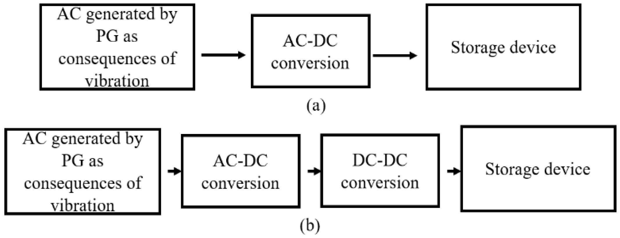
Numerous single- and dual-stage power electronic circuits have been reported in the literature. The single-stage circuit is used for AC-DC conversion, while the dual-stage circuit combines AC-DC and DC-DC conversions. A flow chart of both single- and dual-stage circuits is shown in Figure 2 [11]. A single-stage H-Bridge rectifier (HBR) is the simplest way to convert AC to DC [1,2,9,12,13,14,15,16,17], and it was proposed herein to overcome the issues of the forward voltage of the conventional diodes in the full-bridge (FBR) circuit. Nevertheless, the extracted output voltage and power through the HBR circuit were limited, and the boundary conditions were not well defined.
To overcome the abovementioned limited output voltage and power issues, Edla. et al. extensively studied the possible enhancement of HBR through the incorporation of a dual-stage H-Bridge circuit (DSHBR) [18]. A small solar battery with a rating of 1.2 Vdc and 4 mA was successfully charged by the proposed DSHBR circuit. However, the power dissipation in the DSHBR circuit was higher than the applied input power due to its complexity in conversion stages one and two. Furthermore, the DSHBR circuit included additional components, such as multiple capacitors, additional IC’s, Zener diodes, which resulted in high power dissipation, design complexity and high cost. Generally, the concocted output of the proposed DSHBR circuit was still low, and this study did not provide suitable electrical boundary conditions for the optimisation method.
To overcome the foregoing difficulties and gain high output voltage and power, a buck-boost circuit was proposed by Elie et al. [19] instead of a linear circuit that successfully charged a rechargeable battery with a rating of 4.8 Vdc. The proposed circuit still contained two stages (AC-DC and DC-DC), multiple capacitors and a sensorless ICs to trigger the switches, which caused the power dissipation to rise over the acceptable value.
Another possible way for maximising the output power is a non-linear technique through using additional switches such as metal-oxide-semiconductor field-effect-transistor (MOSFETs), duty cycles, switching frequency, and passive components (inductors and capacitors). Novel non-linear techniques were proposed by [14,16,20,21,22,23,24,25,26]. These circuits included many auxiliary circuits, bulky inductors, transformers and diodes, which made them not the optimal choice to be adopted in the current investigation that aimed at reducing the size of the power electronics circuit, device miniaturisation and cost.
A rectification circuit called a rectifier-less circuit was proposed by Shareef et al. [27] to attain rectifier-less single-stage conversion by integrating a synchronous inductor process and cold start-up quality to attain the effective output from their proposed circuit (only 0.65 mVac was required for gathering output power of 254 µW). However, this topology was complicated as it also acknowledged additional components, such as three PGs and various power electronics components. Thus, device miniaturisation was unachievable.
In general, the reduction in the circuit size and the efficient utilisation of materials are the main challenges to achieving maximum output power from the PG in order to power electronic devices.
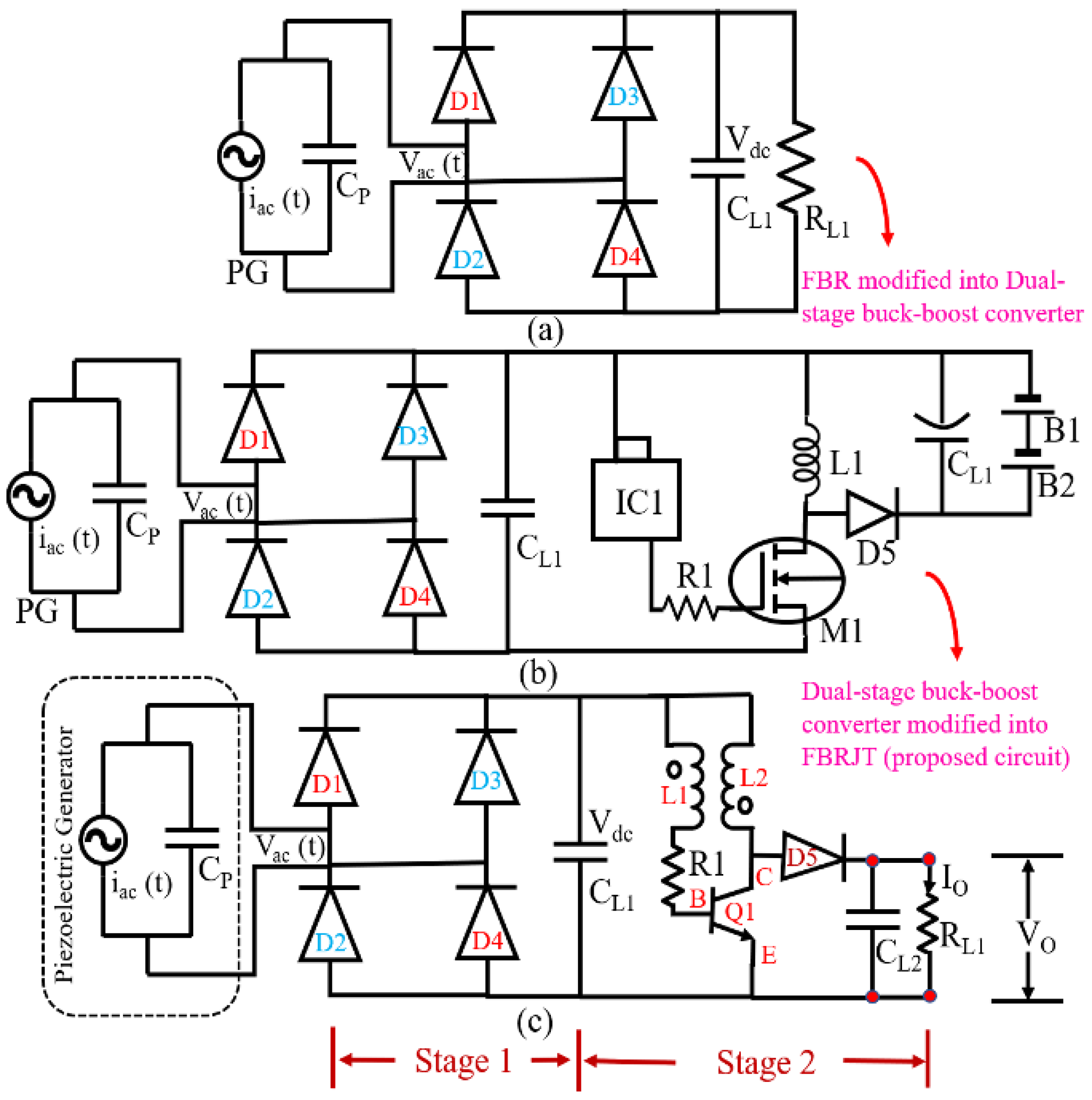
Therefore, the authors employed a combination of the conventional FBR [12] and buck-boost converter [19,28] to overcome the shortcomings of the traditional circuits. The representation of the circuit enhancement procedure is illustrated in Figure 3 [18], while a list of eliminated additional components over the adopted circuits is presented in Table 1.
Thus far, many studies have been carried out to investigate the rectification process, but a combination of both FBR and joule thief circuits has not been introduced yet. In addition, considering the device miniaturisation target, the proposed circuit is developed into FBRJT with limited components without the need to use duty cycles, polarity detectors, logic gates, controllers, and circuits, in comparison with the circuits described in the literature.
The significance of the proposed circuit lies in its ability to reduce the stress between the switching components, polarity detectors and logic gates. It does not also involve auxiliary circuits to minimise conversion losses and costs. As the proposed circuit has a simple, unique design and topology without utilising any active control logic operation, it is expected to reduce the demands on the auxiliary regulating circuits while simultaneously improving the system’s overall performance. It is also anticipated to work effectively for mobile battery charging and energy harvesting applications.
It is worth emphasising that the authors considered a few particular scenarios as the main intention of the PEH field is to convert surrounding environmental vibrations into electrical energy and store it in a storage device. Thus, the following real-life vibrations and their frequencies are used, and the applications of considered vibrations are briefly explained below.
  • The human body resonates at a vertical frequency of 5 Hz [30]; the chest frequency is 4–6 Hz, and the shoulder frequency is 2–6 Hz [31].
  • The washing machine’s drum frequency is 10 Hz [32], the binaural beat frequency is 15–40 Hz [33], car vibration frequency is 1–15 Hz, that of civil infrastructure is 0.3–10 Hz, and that of trees is 0.1–0.8 Hz [34,35].

2. PG Internal Characteristics and Power Conversion Circuits

This section discusses the modelling details of the internal PG circuit, including the FBR circuit, when subjected to excitation, followed by the analysis of the developed FBRJT circuit.

2.1. PG Circuit Model

The PEH system consists of three main aspects: the mechanical interface, power electronics circuit, and storage device. As the PEH process involves both mechanical and electrical prospects, the internal behavior of both prospects will be addressed herein. The PGs are often placed on cantilever beams (Figure 1) to efficiently transmit ME into AC. When the PG is subjected to excitation, it can act as a current source parallel to its internal capacitance, CP [36]. Alternatively, it can be considered a voltage source in series with its internal capacitance.
The internal behavior of the PG in positive and negative cycles when it is excited is shown in Figure 4 [37,38]. It can be seen that the generated PG current, iac, must charge and discharge its internal capacitor, CP, in both half cycles. There is no output expected from the PG during the charging process of an internal capacitor. This period is also called a non-harvesting period (NHP). The output is expected from the PG in the remaining period and is called the harvesting period (HP) [16,18,20,21,39]. Non-harvesting and harvesting periods are denoted by intervals 1, 3 (period t0–1, t2–3) and 2, 4 (period t1–2, t3–4), respectively.
The generated current by the PG due to its mechanical excitation can be written as follows [9,40,41]:
i ac   ( t ) = I ac ^   sin ( ω t ) ,
where I ac ^ and ω are the magnitude of current and angular frequency, respectively, and t is the time.
The outcome of PG is then applied to the PEC for the rectification process. The operation of FBR and the proposed FBRJT circuits is summarised in the following sections.

2.2. FBR Circuit

The FBR circuit (Figure 3) is functioning in Stage 1 and embodies two modes. As the generated AC includes both positive and negative half-cycles, the FBR circuit turns ON and OFF various diodes and stores rectified voltage in the load capacitor, CL1. Thus, the operation of the FBR circuit is described as follows:
  • Mode 1: Positive half cycle
  • During interval 1 (NHP period):
    -
    No output
    -
    D1–D4: OFF
  • During interval 2 (HP period):
    -
    PG delivers output
    -
    D1, D4: ON
    -
    Vac = Vdc (CL1: Charged)
  • Mode 2: Negative half cycle
  • During interval 3 (NHP period):
    -
    No output
    -
    D1–D4: OFF
  • During interval (HP period):
    -
    PG delivers output
    -
    D3, D2: ON
    -
    Vac = Vdc (CL1: Charged)
During both positive and negative half cycles of the PG, the load capacitor, CL1, is charged. The output power of the FBR circuit varies with the rectified voltage [12,36,41], and the peak output power occurs when
V rect = I ac ^   ( t ) 2   ω C P .
Assuming VFBR” CP, the majority of the output current will deliver as
V FBR V FBR +   C P   I ac   ^   i ac .
The rectified output power, PO (t), and the load capacitor, CL1, are related through the following equation:
P O   ( t ) = 2   V dc π ( I ac   V dc ω C P ) .

2.3. FBRJT Circuit

The proposed FBRJT circuit includes Stages 1 and 2 and embodies six modes. As the FBRJT circuit is considered an extension of FBR and dual-stage buck-boost circuits (i.e., Figure 3), the operation of Modes 1 and 2 of the FBR and FBRJT circuits is expected to be the same. Therefore, the operation of Modes 3–6 is only explained in this section.
Mode 3: Initially, switch, Q1 is OFF when the current surges over the CL1 (positive terminal), primary winding (L1), resistor (R1), base-emitter (B-E) and CL1 (negative terminal). As small current passes over the secondary winding (L2), the collector-emitter (C-E) is slightly conductive.
Mode 4: However, as both windings are coupled in opposite directions, they induce the voltage and turn the transistor on with a higher bias. Thus, both windings being connected in opposite directions, they both create magnetic fields around them.
Mode 5: At this instant, the induced voltage in L1 widely opens the base to the emitter (i.e., B-E) terminal. Thus, more current passes over the C-E path. In other terms, rising the voltage in the L1 enhances the current flow across the L2 and C-E.
Mode 6: At this instant, when the core is saturated, there is no more change in the induced magnetic field. Consequently, the induced voltage in the L1 vanishes; wholly open circuit and the path between the C-E have been closed. Thus, the current passes through the other way over the diode, D1, and charges the load capacitor, CL1, and powers the load resistor, RL1. Later, the same procedure proceeds back to Mode 1.
As this research aimed at investigating the PEC development, the separated rectified output power over the FBRJT is a considerable metric to examine the performance of the FBRJT circuit against the currently used circuits in the literature. Note that the primary function of the proposed energy harvesting circuits is to obtain the maximum power over the PEC. Nevertheless, the proposed study only shows the extracted output power and applied input voltage. As a result, the average input power, Pac, that is generated by the PG is calculated as [18,28]
P ac =   V ac ×   i ac = V Pk 2   .   I Pk 2     cos φ ,
where Vac, iac and VPk, IPk are the average and peak voltage and current, respectively, while φ refers to the phase angle between the PGs voltage and the current.
As a result of applying Modes 1–6, the stored output DC voltage through the FBRJT circuit can be considered constant. Accordingly, the output power, PO, through the FBRJT can be calculated as the product of the rectified voltage across its load capacitor, CL2, and current through the load resistor, RL1. Then, the proposed circuit’s efficiency is calculated using the output and input parameters.

3. Simulation Results

The intended application of the proposed circuit is in battery charging and energy harvesting regardless of the applied frequency (i.e., vibrations). Thus, it was tested under two different types of power sources, namely ideal sinusoidal AC voltage and sinusoidal impedance. The performance of the proposed circuit with the ideal sinusoidal source can be considered a proof of concept.
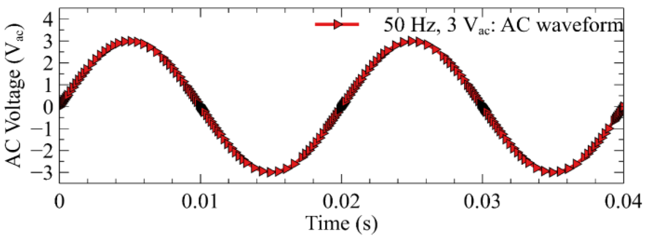
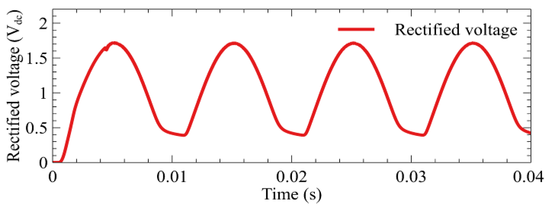
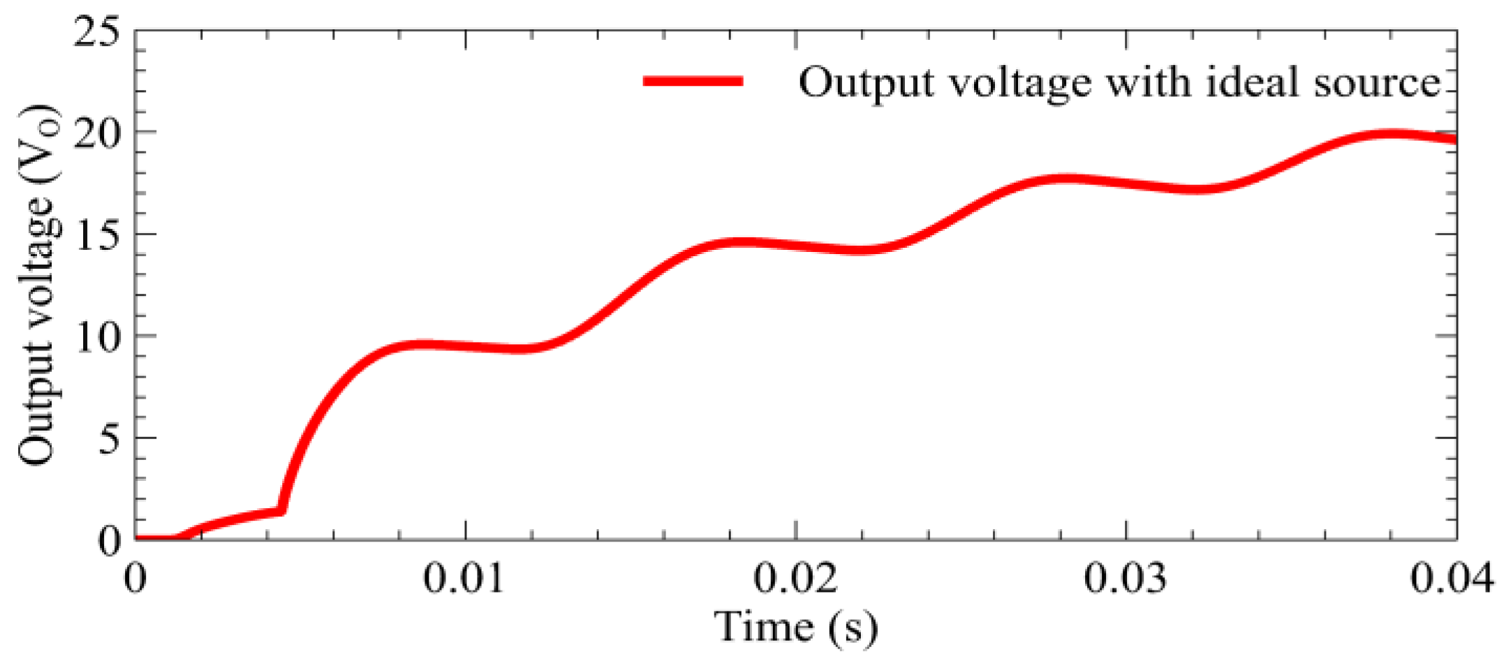
The ideal sinusoidal AC voltage is adopted in LTspice software and applied to the proposed circuit. However, the sinusoidal source is replaced with a PG in the experiment. The applied sinusoidal signal to the proposed FBRJT and the rectified voltage at the load capacitor, CL1 (Mode 2), are shown in Figure 5 and Figure 6, respectively. As a consequence of these waveforms, when the load capacitor CL1 is fully charged, Stage 2 is activated. Therefore, the energising process of primary and secondary windings (Modes 3–4), energised L2 due to the activation of the switch, zoom-in view of L2 and CL2 due to switching process (Mode 5) and the output voltage (Mode 6) as a consequence of the Modes 1–6, are all presented within the context of Figure 7, Figure 8, Figure 9 and Figure 10, respectively.
It is worth noting that the stored rectified voltage in the load capacitor, CL1, is an output of the FBR circuit. The rectified voltage is shown in a separate figure to demonstrate the difference between the outcomes of the FBR and FBRJT circuits. In addition, unless FBR fully charges the CL1, the FBRJT circuit does not conduct.

4. Experimental Results

This experimental test was conducted in the department of the Faculty of Science, Southern Cross University, Lismore, which is situated in the state of NSW, Australia.
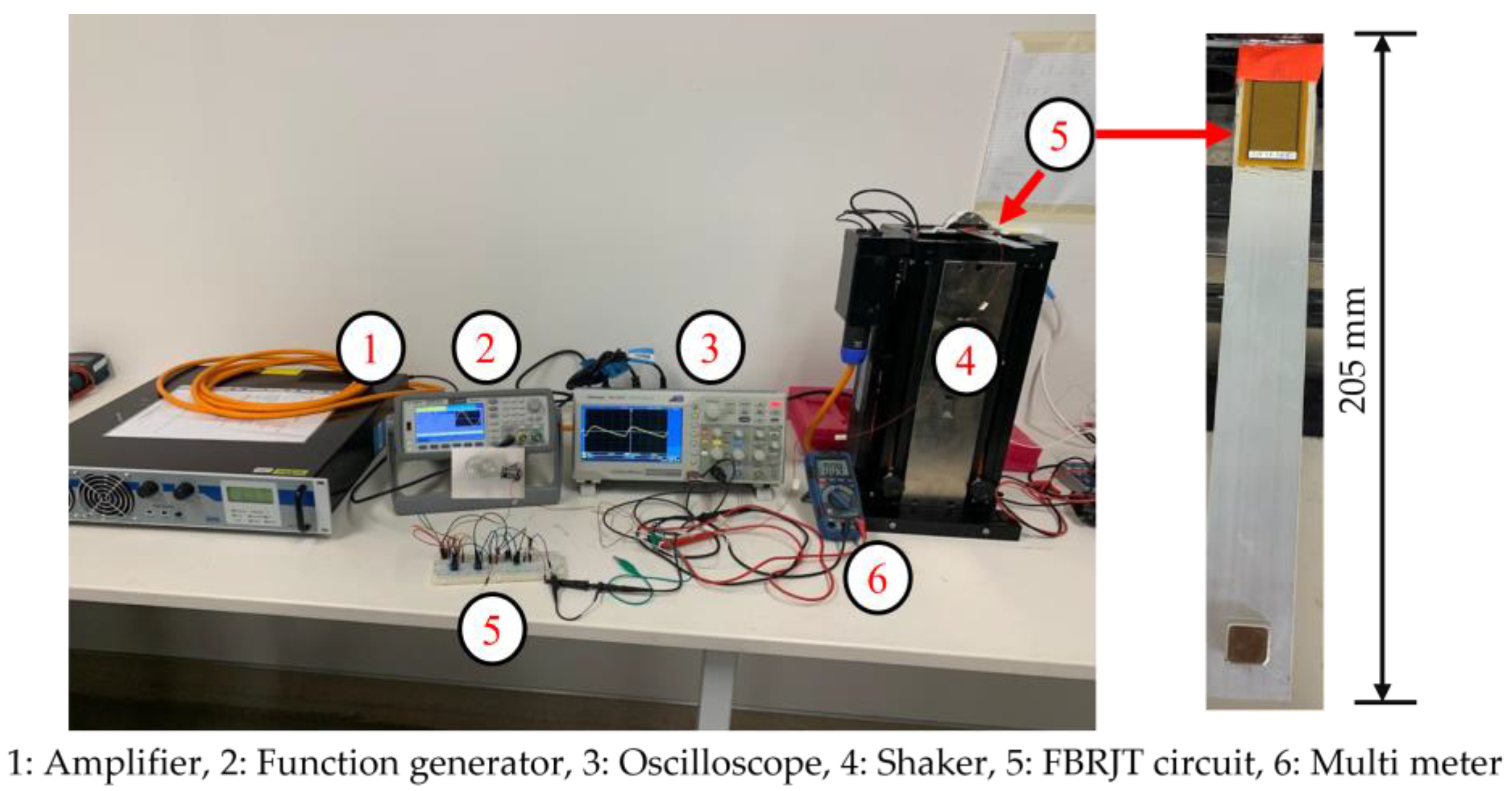
A conventional piezoelectric cantilever beam was made up of an aluminium beam (dimensions: 205 × 20 × 1 mm) with one end fixed into the vibration shaker (Model APS—113), while the other end carried two permanent magnets acting as a proof mass. A microfiber composite (MFC) patch (category: M2814-P2, 38 mm × 20 mm, 300 µm, CP = 33.90 nF) was patched near the fixed end of the aluminium beam where the highest possible strain occurred [3,40,42].
A function generator (Agilent 33210A, USA) was used to deliver a sinusoidal signal to a power amplifier (2706, B & K Agilent, USA), which then amplified the signal before activating the shaker. The shaker generated mechanical excitations according to the input vibration frequency and amplitude to excite the piezoelectric cantilever beam. The acceleration of the base excitation beam can be monitored by using an inductive sensor. As a result of excitation, the patched PG generates AC, which is considered an input voltage to the FBRJT circuit. Figure 11 illustrates the proposed experimental setup and implementation on a breadboard. Two different test scenarios were adopted to evaluate the FBRJT circuit.
In Tests 1 and 2, the AC extracted from the PG through the FBRJT was characterised by varying parameters in the circuit, as described in Table 2. The parameters used in the experiments are listed in Table 1. In Test 1, the FBRJT was tested with constant voltage under varying frequencies, while in Test 2, various accelerations were applied at a constant frequency. The output voltage through the FBRJT circuit in Tests 1 and 2 was stored in a load capacitor for a low electric current at a fixed voltage level. Subsequently, each load resistance was connected in parallel with the load capacitor, and the outcome was captured. A multimeter was used to measure the output voltage across the load capacitor, CL2.

4.1. Test 1: Varying Frequency with a Constant Input Voltage

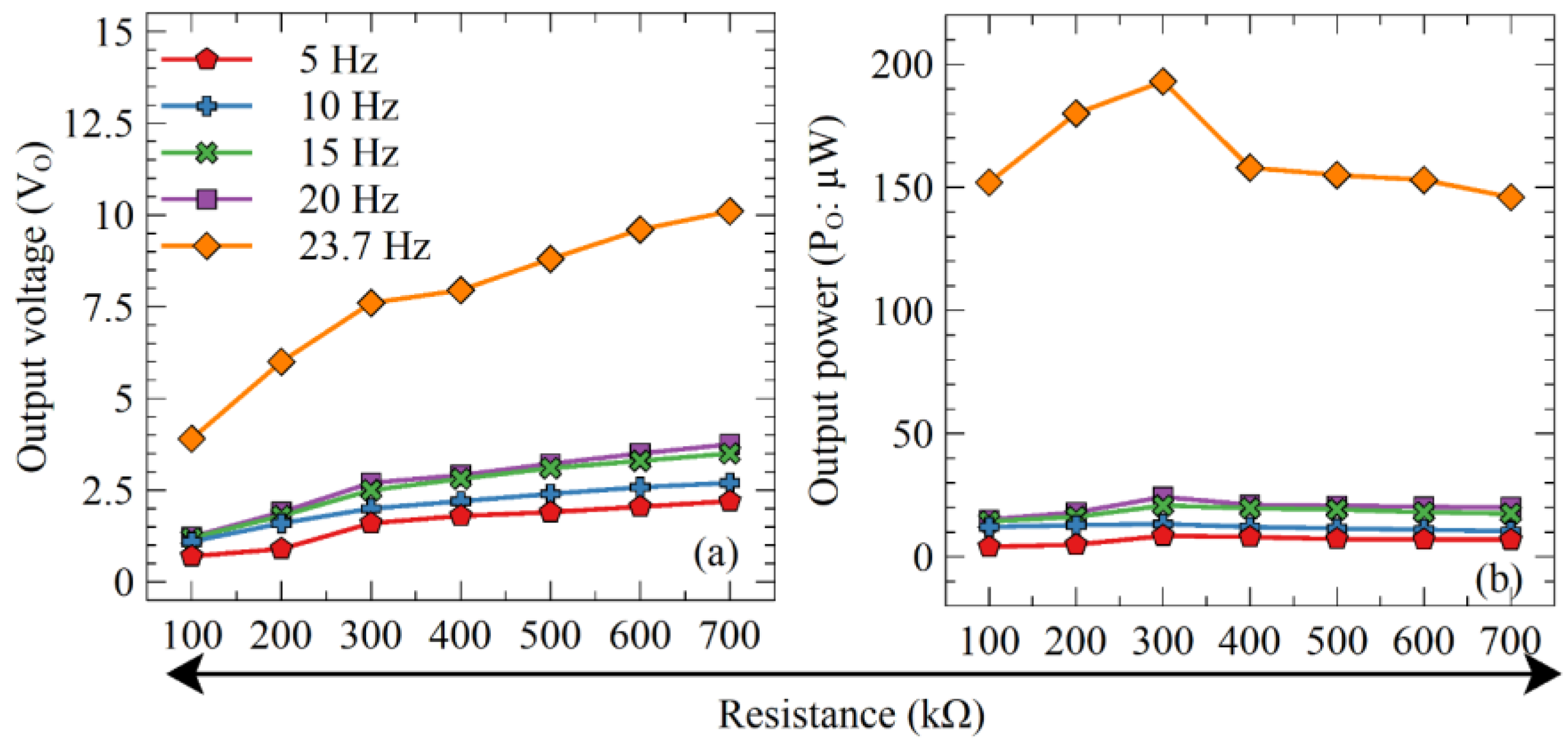
Figure 12a,b shows the acquired output voltage and output power over the load resistances from 100 to 700 kΩ of Test 1.
Figure 12a shows that irrespective of the applied frequency, the output voltage is increased by adding the load resistances from 100 to 700 kΩ with a constant input volt-age. It can also be noted that the proposed topology produced the maximum output voltage at a load resistance of 700 kΩ. To attain the best performance, the input voltage is expected to be higher compared to the forward voltage (Vf) and the threshold voltage of the diodes and transistors (switch, Q1).
Primarily, 3 Vac was applied to the FBRJT circuit at 5 Hz, which includes two stages. Thus, the applied AC voltage is rectified and stored in the load capacitor, CL1, in Stage 1. Afterwards, the stored rectified voltage in CL1, as a consequence of Stage 1, stimulates the current to flow through primary (L1) and secondary (L2) windings, while a weak current passes through the collector to the emitter (C-E). As both windings are connected in opposite directions, the current induces a magnetic field in both windings. The induced voltage in the secondary windings turned on the switch with a higher bias. This occurred due to the rapid turning of the switch ON and OFF. When the core was saturated, there was no more change in the magnetic field. Thus, the induced voltage in L1 has vanished. Consequently, the switch was turned OFF, and the stored magnetic field in L2 was transferred through diode D1 and accumulated in the load capacitor, CL2. It is worth noting that the stored voltage in the load capacitor was denoted by the rectified voltage, Vdc, while the output voltage, VO, denoted the stored voltage in the load capacitor. Each load resistor was connected in a shunt with the load capacitor, CL2, and the outcome was captured through the oscilloscope.
Similarly, other frequencies were applied with the same input voltage, and the outcome was captured, as shown in Figure 12a. When the output voltage was stored in CL2, the voltage crossed it, and the current through the load resistor RL2 was measured, allowing for the output power to be calculated (Figure 12b).
Observing other cases, the trend of increasing output voltage with increasing resistance is consistent. Compared to the output voltage, the trend of output power against the load resistances is rather different.
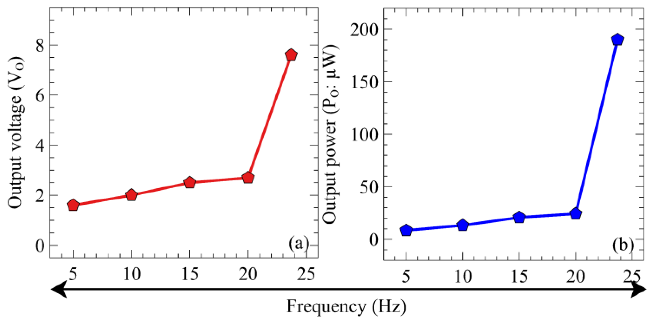
Further inspecting Figure 12, one can identify that the excitation frequency remarkably affects the performance of the proposed circuit, the extracted output voltage and power. This was particularly evident in the case of the FBRJT circuit, where the highest output voltage and power were achieved at the resonance frequency. The achieved highest output voltage and power against the various frequencies are plotted in Figure 13.
Although the applied input voltage was adjusted to 3 Vac at various frequencies, it can be seen that the higher output voltage and power were achieved at a high frequency [9]. There were two leading causes of yielding the higher output through FBRJT, which are described below.
  • When frequency increased, the PG produced a higher current due to the reduction in its capacitive reactance.
  • As the PG current increased, the output power of PG also increased, which led to an increase in the output power of the FBRJT circuit.
Here, we recollect that the significant objective of this research is to validate the performance of the FBRJT circuit to track the PGs ideal points, power reliance on the frequency at various load resistances, achieving a high output voltage and power at 23.7 Hz with input voltages of 3 Vac.

4.2. Test 2: Varying Acceleration at Constant Frequency

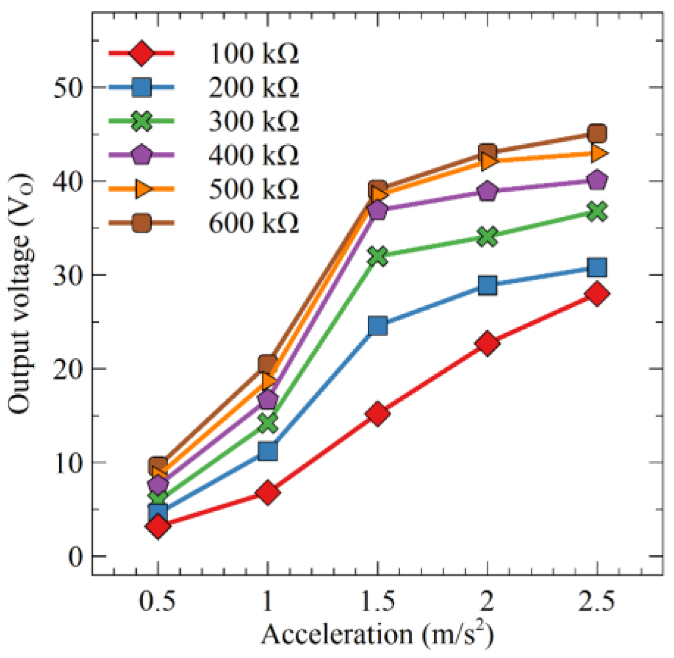
In order to verify the performance of the proposed circuit, it was tested under constant frequency with varying accelerations. In this scenario, the frequency of the PG was kept constant, and various accelerations were applied to the FBRJT circuit (Table 2). The outcome is presented in Figure 14.
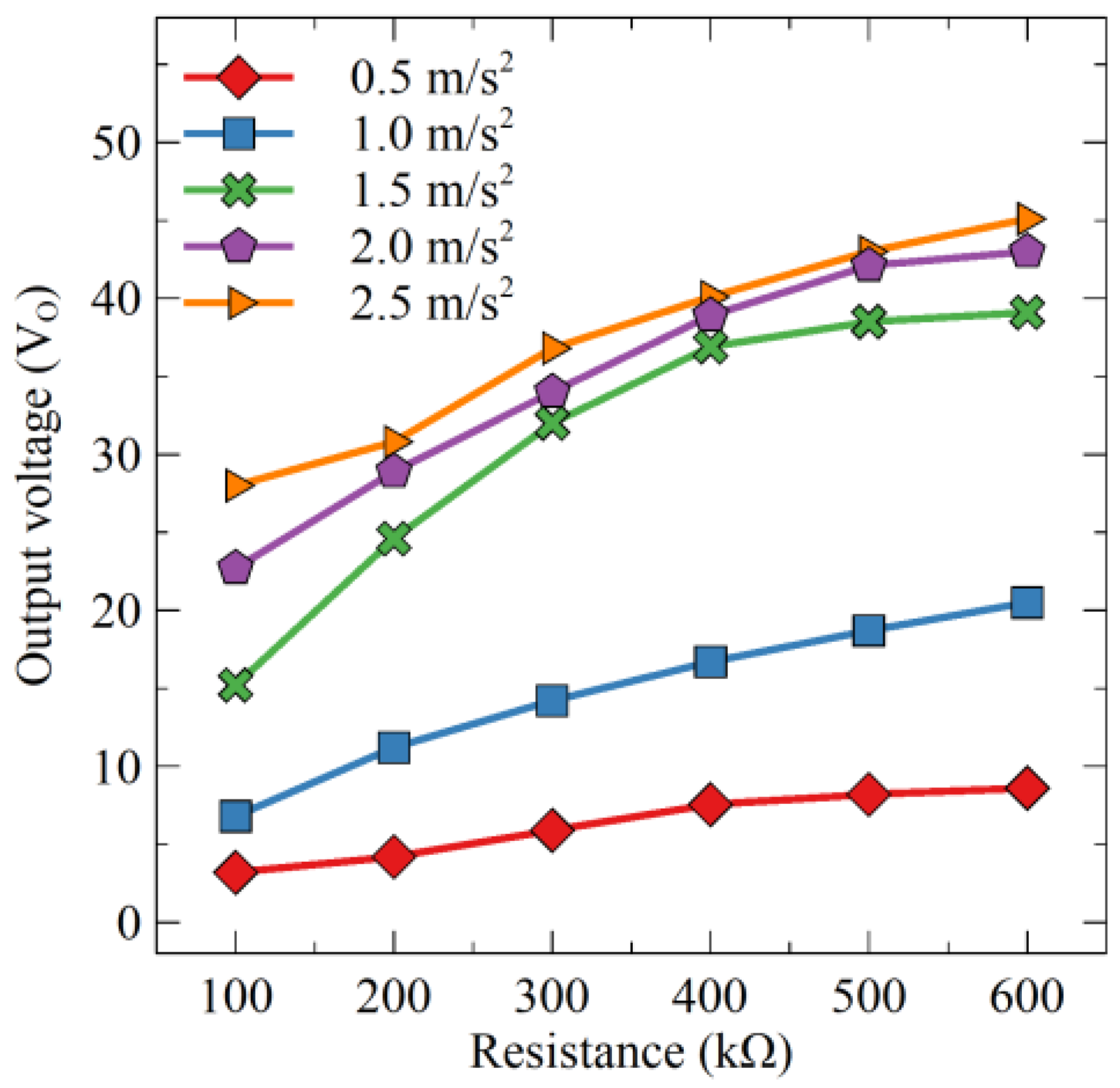
Initially, 0.5 acceleration was applied at a frequency of 10 Hz in Test 2. As the generated voltage by the PG is proportional to the acceleration, the applied input voltage was increased with increasing the acceleration [19,43]. As the applied input voltage was higher than the forward voltage of the diodes and threshold voltage of the switch, Q1, the FBRJT circuit was in conduction mode in both stages 1 and 2 (as explained in Test 1), respectively. As a result, the output voltage was stored in the load capacitor, and the captured outcome voltage was plotted in Figure 14. To further understand the performance of the proposed circuit, the relationship between the measured output voltage and resistance was observed and represented in Figure 15.
From Figure 15, it can be seen that the output voltage increased with the increase in the load resistance, regardless of the acceleration (m/s2). The trend of increase in the output voltage was consistent with the load resistance. This observation is in line with Test 1.

4.3. Test 3: Comparison of FBRJT Circuit with The Literature Circuits

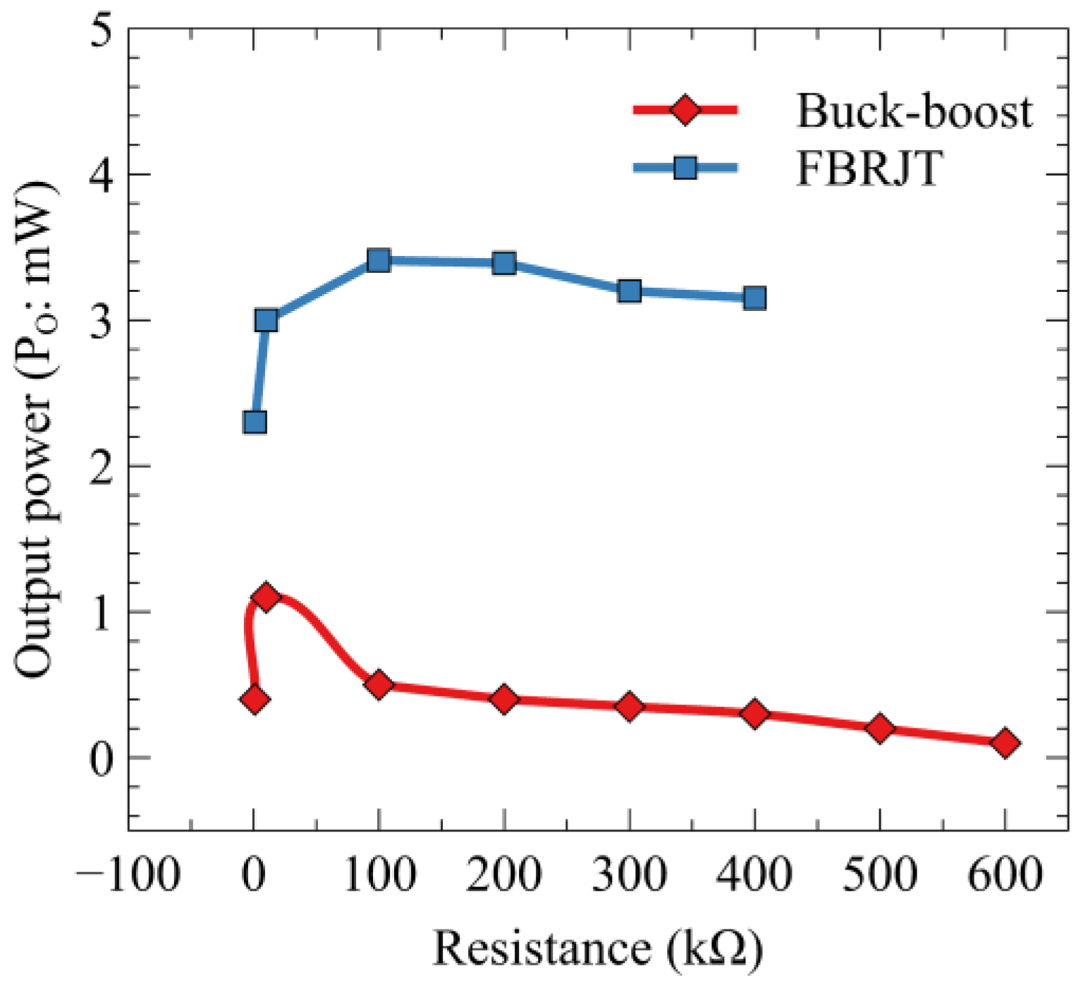
From Tests 1 and 2, it can be observed that the use of the FBRJT circuit consistently produces high output in both scenarios of varying frequencies with constant input voltage and varying acceleration at a constant frequency. In order to further understand the performance of the FBRJT circuit, a comparative study between the proposed circuit output power and the similarly designed buck-boost circuit was undertaken (Figure 16).
The output power of relevant published circuits used in the comparison study has been attained using an SPBC circuit with specifications summarised in Table 3.
Overall, it was determined that the FBRJT circuit consistently produces a higher output compared to the well-established buck-boost circuit and tabulated literature circuits at the frequencies considered in this study (i.e., Table 2). Thus, the proposed circuit is anticipated to work in the application of mobile charging and energy harvesting applications at the considered frequencies. Moreover, from Table 3, it was determined that the proposed FBRJT circuit outperformed several similar published literature circuits in terms of output voltage and power.

5. Conclusions

A full-bridge joule thief (FBRJT) circuit was proposed and studied in this paper to identify the PG’s optimal points, output voltage, power dependency on various frequencies, and load resistances and to achieve a high output voltage and power with very low input voltages. The FBRJT circuit integrated a combination of the well-established conventional full-bridge circuit in Stage 1 and the joule theory circuit in Stage 2 to extend the concepts of FBR and buck-boost circuits. The FBRJT circuit was capable of meeting the requirements of device miniaturisation and providing an efficient AC-DC conversion process without employing additional components and auxiliary circuits. The performance of the FBRJT circuit was verified through both simulation and experiment testing, from which its ability to maximise the output voltage and power was observed. The FBRJT circuit converted an AC signal with a frequency of 23.7 Hz and 3 Vac into an output voltage of 7.6 Vdc with a maximum achievable output power of 193 µW. In addition, it converted the generated AC signal with the acceleration of 1.5 m/s2 at a frequency of 10 Hz into an output voltage of 32 Vdc with a maximum attainable power of 3.41 mW. Due to the great potential of using the proposed circuit in many applications, such as battery charging and energy harvesting, it was essential to test it under ideal and impedance sources. In addition, the proposed circuit is anticipated to work in the application of mobile battery charging and energy harvesting applications. In conclusion, the FBRJT circuit proved its functionality as an effective solution for the traditional circuit’s low output voltage and power. These significant findings stimulated the research team to investigate further the ability to control the output voltage (i.e., Stage 2) with a high-rating capacitor/small battery, which needs to be addressed in future publications.

Author Contributions

Conceptualization, M.K.; methodology, M.K. and M.E.; software, M.K. and M.E.; validation, M.K. and M.E.; formal analysis, M.K. and M.E.; investigation, M.K. and M.E.; resources, M.K., M.E. and A.M.T.; data curation, M.K., M.E. and A.M.T.; writing—original draft preparation, M.K. and M.E.; writing—review and editing, M.K., M.E. and A.M.T.; visualization, M.K., M.E., A.M.T., D.M., V.B. and A.H.; supervision, M.E., A.M.T. and D.M.; project administration, M.E., A.M.T. and D.M.; funding acquisition, M.E., A.M.T. and D.M.; All authors have read and agreed to the published version of the manuscript.

Funding

This research is supported by Southern Cross University Lismore with no external funding.

Data Availability Statement

Data is available on request.

Conflicts of Interest

The authors declare no conflict of interest.

References

  1. Rahman, A.; Farrok, O.; Islam, M.R.; Xu, W. Recent Progress in Electrical Generators for Oceanic Wave Energy Conversion. IEEE Access 2020, 8, 138595–138615. [Google Scholar] [CrossRef]
  2. Xi, S.; Li, W.; Guo, J.; Liang, J. A Self-Powered Piezoelectric Energy Harvesting Interface Circuit Based on Adaptive SSHI with Fully Integrated Switch Control. In Proceedings of the 2020 IEEE International Symposium on Circuits and Systems (ISCAS), Seville, Spain, 12–14 October 2020; pp. 1–4. [Google Scholar]
  3. Izadgoshasb, I.; Lim, Y.Y.; Lake, N.; Tang, L.; Padilla, R.V.; Kashiwao, T. Optimizing orientation of piezoelectric cantilever beam for harvesting energy from human walking. Energy Convers. Manag. 2018, 161, 66–73. [Google Scholar] [CrossRef]
  4. Izadgoshasb, I.; Lim, Y.Y.; Tang, L.; Padilla, R.V.; Tang, Z.S.; Sedighi, M. Improving efficiency of piezoelectric based energy harvesting from human motions using double pendulum system. Energy Convers. Manag. 2019, 184, 559–570. [Google Scholar] [CrossRef]
  5. Mahesh Edla, Y.Y.L. An Improved Piezoelectric Energy Harvesting Circuit for Reducing the Internal Loss. In Proceedings of the 83rd Researchfora International Conference, New Delhi, India, 29–30 January 2020. [Google Scholar]
  6. Beeby, S.P.; Torah, R.; Tudor, M.; Glynne-Jones, P.; O’Donnell, T.; Saha, C.; Roy, S. A micro electromagnetic generator for vibration energy harvesting. J. Micromech. Microeng. 2007, 17, 1257. [Google Scholar] [CrossRef]
  7. Erturk, A.; Inman, D.J. An experimentally validated bimorph cantilever model for piezoelectric energy harvesting from base excitations. Smart Mater. Struct. 2009, 18, 025009. [Google Scholar] [CrossRef]
  8. Erturk, A.; Inman, D.J. Piezoelectric Energy Harvesting; John Wiley & Sons: Hoboken, NJ, USA, 2011. [Google Scholar]
  9. Edla, M.; Lim, Y.Y.; Vasquez Padilla, R.; Deguchi, M. An Improved Rectifier Circuit for Piezoelectric Energy Harvesting from Human Motion. Appl. Sci. 2021, 11, 2008. [Google Scholar] [CrossRef]
  10. Edla, M.; Lim, Y.Y.; Deguchi, M.; Padilla, R.V. A Novel Discontinuous Mode Piezoelectric Energy Harvesting Circuit for Low-Voltage Applications. In Proceedings of the 2021 31st Australasian Universities Power Engineering Conference (AUPEC), Perth, Australia, 26–30 September 2021; pp. 1–5. [Google Scholar]
  11. Edla, M.; Lim, Y.Y.; Mikio, D.; Padilla, R.V. A Single-Stage Rectifier-Less Boost Converter Circuit for Piezoelectric Energy Harvesting Systems. IEEE Trans. Energy Convers. 2021, 37, 505–514. [Google Scholar] [CrossRef]
  12. Edla, M.; Lim, Y.Y.; Deguchi, M.; Padilla, R.V.; Izadgoshasb, I. An Improved Self-Powered H-Bridge Circuit for Voltage Rectification of Piezoelectric Energy Harvesting System. IEEE J. Electron Devices Soc. 2020, 8, 1050–1062. [Google Scholar] [CrossRef]
  13. Maiorca, F.; Giusa, F.; Trigona, C.; Andò, B.; Bulsara, A.R.; Baglio, S. Diode-less mechanical H-bridge rectifier for “zero threshold” vibration energy harvesters. Sens. Actuators A Phys. 2013, 201, 246–253. [Google Scholar] [CrossRef]
  14. Xia, H.; Xia, Y.; Shi, G.; Ye, Y.; Wang, X.; Chen, Z.; Jiang, Q. A Self-Powered S-SSHI and SECE Hybrid Rectifier for PE Energy Harvesters: Analysis and Experiment. IEEE Trans. Power Electron. 2020, 36, 1680–1692. [Google Scholar] [CrossRef]
  15. Huang, Y.-T.; Li, C.-H.; Chen, Y.-M. A Modified Asymmetrical Half-Bridge Flyback Converter for Step-Down AC–DC Applications. IEEE Trans. Power Electron. 2019, 35, 4613–4621. [Google Scholar] [CrossRef]
  16. Du, S.; Jia, Y.; Zhao, C.; Amaratunga, G.A.; Seshia, A.A. A nail-size piezoelectric energy harvesting system integrating a MEMS transducer and a CMOS SSHI circuit. IEEE Sens. J. 2019, 20, 277–285. [Google Scholar] [CrossRef]
  17. Du, S.; Jia, Y.; Zhao, C.; Amaratunga, G.A.; Seshia, A.A. A fully integrated split-electrode SSHC rectifier for piezoelectric energy harvesting. IEEE J. Solid-State Circuits 2019, 54, 1733–1743. [Google Scholar] [CrossRef]
  18. Edla, M.; Lim, Y.Y.; Padilla, R.V.; Mikio, D. Design and Application of a Self-Powered Dual-Stage Circuit for Piezoelectric Energy Harvesting Systems. IEEE Access 2021, 9, 86954–86965. [Google Scholar] [CrossRef]
  19. Lefeuvre, E.; Audigier, D.; Richard, C.; Guyomar, D. Buck-Boost Converter for Sensorless Power Optimization of Piezoelectric Energy Harvester. IEEE Trans. Power Electron. 2007, 22, 2018–2025. [Google Scholar] [CrossRef]
  20. Eltamaly, A.M.; Addoweesh, K.E. A novel self-power SSHI circuit for piezoelectric energy harvester. IEEE Trans. Power Electron. 2017, 32, 7663–7673. [Google Scholar] [CrossRef]
  21. Lu, S.; Boussaid, F. A highly efficient P-SSHI rectifier for piezoelectric energy harvesting. IEEE Trans. Power Electron. 2015, 30, 5364–5369. [Google Scholar] [CrossRef]
  22. Pollet, B.; Despesse, G.; Costa, F. A New Non-Isolated Low-Power Inductorless Piezoelectric DC–DC Converter. IEEE Trans. Power Electron. 2019, 34, 11002–11013. [Google Scholar] [CrossRef]
  23. Xia, H.; Xia, Y.; Ye, Y.; Qian, L.; Shi, G.; Chen, R. Analysis and simulation of synchronous electric charge partial extraction technique for efficient piezoelectric energy harvesting. IEEE Sens. J. 2018, 18, 6235–6244. [Google Scholar] [CrossRef]
  24. Lefeuvre, E.; Badel, A.; Brenes, A.; Seok, S.; Woytasik, M.; Yoo, C. Analysis of piezoelectric energy harvesting system with tunable SECE interface. Smart Mater. Struct. 2017, 26, 035065. [Google Scholar] [CrossRef]
  25. Lee, M.; Yang, J.; Park, M.; Jung, S.; Kim, J. Design and Analysis of Energy-Efficient Single-Pulse Piezoelectric Energy Harvester and Power Management IC for Battery-Free Wireless Remote Switch Applications. IEEE Trans. Circuits Syst. I Regul. Pap. 2018, 65, 366–379. [Google Scholar] [CrossRef]
  26. Dini, M.; Romani, A.; Filippi, M.; Tartagni, M. A nanopower synchronous charge extractor IC for low-voltage piezoelectric energy harvesting with residual charge inversion. IEEE Trans. Power Electron. 2015, 31, 1263–1274. [Google Scholar] [CrossRef]
  27. Shareef, A.; Goh, W.L.; Narasimalu, S.; Gao, Y. A rectifier-less ac–dc interface circuit for ambient energy harvesting from low-voltage piezoelectric transducer array. IEEE Trans. Power Electron. 2018, 34, 1446–1457. [Google Scholar] [CrossRef]
  28. Rashid, M.H. Power Electronics Handbook; Butterworth-Heinemann: Oxford, UK, 2017. [Google Scholar]
  29. Bimbhra, P.; Kaur, S. Power Electronics; Khanna Publishers: Delhi, India, 2012; Volume 2. [Google Scholar]
  30. Poulton, E.C. Increased vigilance with vertical vibration at 5 Hz: An alerting mechanism. Appl. Ergon. 1978, 9, 73–76. [Google Scholar] [CrossRef]
  31. Badran, S.; Salah, A.; Abbas, W.; Abouelatta, B. Design of Optimal Linear Suspension for Quarter Car with Human Model using Genetic Algorithms. Res. Bull. Jordan ACM 2012, 2, 42–51. [Google Scholar]
  32. Spelta, C.; Previdi, F.; Savaresi, S.M.; Fraternale, G.; Gaudiano, N. Control of magnetorheological dampers for vibration reduction in a washing machine. Mechatronics 2009, 19, 410–421. [Google Scholar] [CrossRef]
  33. Wang, X.; Lu, H.; He, Y.; Sun, K.; Feng, T.; Zhu, X. Listening to 15 Hz Binaural Beats Enhances the Connectivity of Functional Brain Networks in the Mental Fatigue State—An EEG Study. Brain Sci. 2022, 12, 1161. [Google Scholar] [CrossRef]
  34. Malaji, P.; Ali, S.F. Analysis of energy harvesting from multiple pendulums with and without mechanical coupling. Eur. Phys. J. Spec. Top. 2015, 224, 2823–2838. [Google Scholar] [CrossRef]
  35. Ab Rahman, M.F.B.; Kok, S.L. Investigation of useful ambient vibration sources for the application of energy harvesting. In Proceedings of the 2011 IEEE Student Conference on Research and Development, Cyberjaya, Malaysia, 19–20 December 2011; pp. 391–396. [Google Scholar]
  36. Tabesh, A.; Frechette, L.G. A Low-Power Stand-Alone Adaptive Circuit for Harvesting Energy From a Piezoelectric Micropower Generator. IEEE Trans. Ind. Electron. 2010, 57, 840–849. [Google Scholar] [CrossRef]
  37. Edla, M.; Lim, Y.Y.; Mikio, D.; Padilla, R.V. Non-Linear Switching Circuit for Active Voltage Rectification and Ripples Reduction of Piezoelectric Energy Harvesters. Energies 2022, 15, 709. [Google Scholar] [CrossRef]
  38. Edla, M.; Deguchi, M.; Lim, Y.Y. A Self-Powered H-Bridge Joule Theory Circuit for Piezoelectric Energy Harvesting Systems. Power Electron. Devices Compon. 2022, 3, 100015. [Google Scholar] [CrossRef]
  39. Priya, S.; Inman, D.J. Energy Harvesting Technologies; Springer: New York, NY, USA, 2009; Volume 21. [Google Scholar]
  40. Edla, M.; Deguchi, M.; Izadgoshasb, I.; Mahmud, M.A.P.; Kouzani, A.Z. Self-powered boost-converter for power optimisation and piezo garden lights. Smart Mater. Struct. 2022, 31, 045021. [Google Scholar] [CrossRef]
  41. Ottman, G.K.; Hofmann, H.F.; Bhatt, A.C.; Lesieutre, G.A. Adaptive piezoelectric energy harvesting circuit for wireless remote power supply. IEEE Trans. Power Electron. 2002, 17, 669–676. [Google Scholar] [CrossRef] [Green Version]
  42. Edla, M. Development of an Adaptive Piezoelectric Harvesting System for Wireless Remote Power Supply. Master’s Thesis, Coventry University, Coventry, UK, 2015. [Google Scholar]
  43. De Pasquale, G.; Fraccarollo, F.; Somà, A. Performances evaluation of an autonomous sensing network node for rail vehicles supplied by a piezoelectric energy harvester. In Proceedings of the Power MEMS, Leuven, Belgium, 30 November–3 December 2010; pp. 73–76. [Google Scholar]
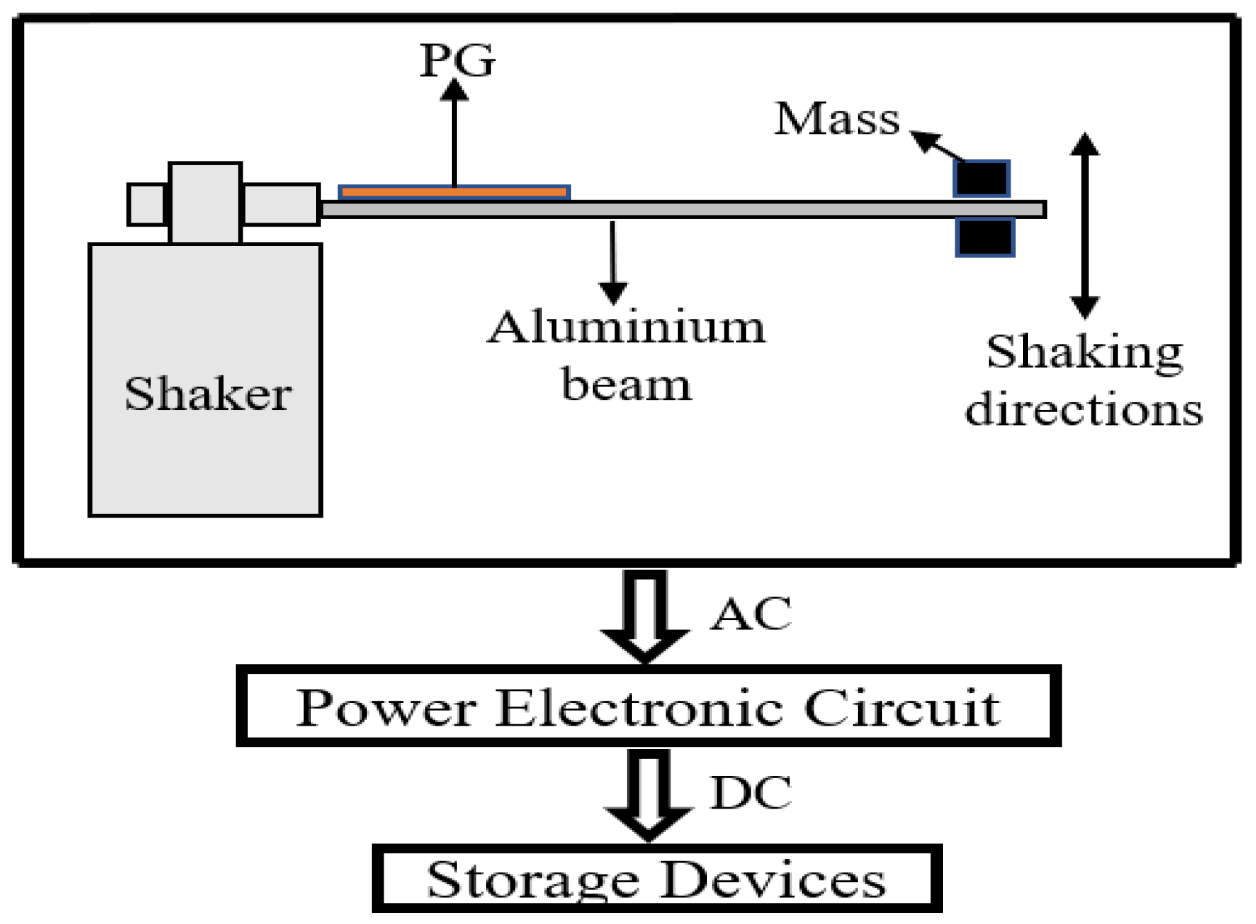
Figure 1. A flow chart representing the PEH systems.
Energies 16 01734 g001
Figure 2. Conversion processes: (a) Single, (b) Dual stages.
Energies 16 01734 g002
Figure 3. Enhancement procedure of the proposed circuit. (a) FBR, (b) Dual-stage buck-boost converter, (c) Proposed circuit, FBRJT, diodes, D1–D5; load capacitors, CL1–2; load resistors, R1, RL1; batteries, B1–2; inductors, L1, L2; switches, M1, Q1; base, collector, emitter, B, C, E; rectified, output voltage, output current, Vdc, VO, IO.
Energies 16 01734 g003
Figure 4. PG and associated waveforms. (a) PG representation as a current source and (b) current and voltage output of PG.
Energies 16 01734 g004
Figure 5. Applied ideal sinusoidal AC voltage.
Energies 16 01734 g005
Figure 6. Stored rectified voltage in CL1.
Energies 16 01734 g006
Figure 7. Energised windings (i.e., Modes 4–5): (a) Primary and (b) secondary.
Energies 16 01734 g007
Figure 8. Zoom-in view (i.e., Mode 5) of (a) activated switch, Q1, and (b) energising secondary winding as a consequence of Q1.
Energies 16 01734 g008
Figure 9. Energising and charging processes (i.e., Mode 6). (a) Zoom-in view of L2 and (b) charging process of load capacitor, CL2.
Energies 16 01734 g009
Figure 10. Stored output voltage load capacitor, CL2, as a consequence of Modes 1–6.
Energies 16 01734 g010
Figure 11. Experimental circuit diagram and experimental setup.
Energies 16 01734 g011
Figure 12. Outcomes of Test 1 through the FBRJT circuit. (a) Output voltage, (b) output power.
Energies 16 01734 g012
Figure 13. Outcomes of Test 1 at various frequencies. (a) Output voltage, (b)output power.
Energies 16 01734 g013
Figure 14. Output voltage of FBRJT in Test 2.
Energies 16 01734 g014
Figure 15. Resistance versus output voltage scenario of Test 2.
Energies 16 01734 g015
Figure 16. Comparison of the proposed circuit with the literature circuit, (a) FBRJT, (b) buck-boost circuits (i.e., Figure 3).
Energies 16 01734 g016
Table 1. List of eliminated parameters in the proposed study.
Similar CircuitsComponent Quantity
DiodesMOSFETsSwitch
Drivers
Additional ICsInductorsLoad
Capacitors
Load
Resistors
Auxiliary Circuits
FBR [29]4 (0.67 Vf)0000110
Dual-stage buck-boost converter [19]51111310
SSRBC [11]34202111
Hybrid rectifier [14]34102110
Proposed, FBRJT51002110
Table 2. Testing scenarios.
ScenariosFrequency (Hz)Input Voltages (Vac)Load Capacitor (µF)Load Resistor (kΩ)
Test 15, 10, 15, 20, 23.7310100–700
Test 210Acceleration ( m s 2 )
0.5, 1, 1.5, 2, 2.5
Table 3. Comparison of outcomes of circuits in the literature.
Literature CircuitsNo of PGsAcceleration
(m/s2)
Input Voltage (Vac)Output Power
(µ/mW)
Efficiency
(ŋ)
[36]1-80.8 mW60%
[18] (similar circuit)1-522 µWNot mentioned
[19] (similar circuit)11.5Frequency1.1 mW68%
66 (resonance)
FBRJT11.5103.41 mW71.5%
Disclaimer/Publisher’s Note: The statements, opinions and data contained in all publications are solely those of the individual author(s) and contributor(s) and not of MDPI and/or the editor(s). MDPI and/or the editor(s) disclaim responsibility for any injury to people or property resulting from any ideas, methods, instructions or products referred to in the content.