Article

A Modular Circuit Synthesis Oriented Modelling Approach for Non-Isolated DC-DC Converters in CCM

by
Lebogang Masike
* and
Michael Njoroge Gitau
Department of Electrical, Electronic and Computer Engineering, University of Pretoria, Pretoria 0002, South Africa
*
Author to whom correspondence should be addressed.
Energies 2023, 16(3), 1047; https://doi.org/10.3390/en16031047
Submission received: 21 November 2022 / Revised: 29 December 2022 / Accepted: 13 January 2023 / Published: 17 January 2023
(This article belongs to the Special Issue Design and Application of DC-DC Converters in Power Systems)

Abstract

:
The continued commissioning of DC microgrids in an effort to achieve net-zero carbon levels in the atmosphere demands the large-scale deployment of converters to make the power from renewable energy sources, such as solar PV, usable. To control these inherently non-linear converters using classical linear control methods, averaged modelling techniques are employed. These methods are laborious and easily become intractable when applied to converters with increased energy storage elements. A modular modelling approach is proposed. This approach is based on the synthesis of converters using refined basic building blocks. The refined basic building blocks are independently modelled as two-port networks and used in a circuit synthesis-oriented manner to derive power stage models of commonly used DC-DC converters. It is found that most of the converters considered in the study can be described as a cascade combination of these basic building blocks. As such, transmission parameters are mainly used to model the two-port networks. Moreover, it is also found that using this modelling technique enables the computation of generalized expressions for all power stage models of interest. The use of two-port networks curtails the size of the matrices describing the basic building blocks to 2 × 2, and thus simplifies the entire modelling procedure. Additionally, two-port network analysis makes this modelling technique modular, thus making it more suited to be employed in DC microgrids. The independence of the two-port models on the circuit topology and functionality makes it possible to even model new converters containing the described basic building blocks solely based on circuit connection.

1. Introduction

The role of a DC-DC converter in a DC microgrid can loosely be equated to that of the AC transformer in the conventional AC grid. Unlike AC transformers, which are mostly passive devices, these converters employ switching schemes to function [1,2,3,4]. Additionally, these converters have a more direct influence on the performance of the entire DC grid, since they can be used to extract maximum power from a source [5,6,7], actively transfer charge into an energy storage device [8,9], correct the system power factor [10], emulate a source [11,12], and mask the intermittence of renewable energy sources (RES) [5,7], etc. Functions such as active power control will typically be the sole responsibility of generators in an AC grid [13]. The versatility of DC-DC converters is enabled by the controller’s ability to determine a correct duty ratio for the active switches for any operating point [7,10,11,12]. Moreover, such versatility makes these converters critical in the mission to achieve net-zero carbon levels and ultimately combat effects of global warming, because power from RES cannot be directly used for most practical applications [3,14,15,16].
The switching nature of these converters makes them inherently non-linear [17,18,19]. This non-linear nature renders the direct use of classical control methods futile since they rely on linear models [18,19]. As such, pseudo-heuristic modelling techniques, such as state-space averaging [20], circuit averaging [21], and a switching flow graph [22], were developed to arrive at a linear model for these converters such that linear control methods such as proportional, integral, and derivative (PID) control can still be used [18,19]. The derivation of models from these pseudo-heuristic modelling techniques is somewhat laborious and the algebra easily gets intractable and complex with higher-order converters [17,21,23]. For DC microgrids, these converters are deployed in large numbers to perform specialized functions, including voltage regulation [24,25]. The deployment of a specific type of converter at any point in the microgrid is dependent on the application of interest and accompanying design specifications [5,6,7,24,25,26,27]. There is a plethora of DC-DC converter topologies to choose from, each with known merits and demerits [28,29,30,31,32,33,34]. To deal with the proliferation of converters, researchers have introduced organizational tools to identify, classify, and deduce insights pertinent to the genesis and overlapping traits among available DC-DC converters. Among these organizational tools is the use of converter cells [28], the minimum separable switching configuration (MISSCO) [35], PWM switches [36,37], layer schemes [38], graft schemes [39], circuit topology transformations [29,31], the tapped-inductor switcher (TIS) [40,41], cascaded/quadratics [42], voltage multiplier cells (VMC) [43], and, most recently, type 1, 2, and 3 converter basic building blocks (BBBs) alongside a filter block [33].
The use of converter organizational tools to model the power stage of these converters provides a circuit synthesis approach to modelling and has proven effective in providing more insight on the fundamental operation of converters, highlighting the evolution of converters, and unifying and generalizing converter models, as well as reducing model computational effort [28,33,35,36,37,38,39,40,41]. Using a single converter cell enables one to generate a maximum of six converters from simple connection permutations of the cell with the input and output ports [28]. To model the power stage of these converters, the same permutations can be performed with an equivalent averaged model of the converter cell, i.e., steady-state, large-signal, and small-signal models of six converters can be computed through connection permutations of one converter cell. It should be noted that even after substituting the averaged model of the converter cell, substantial analysis still needs to be carried out for computing the power stage models of converters. Additionally, equation manipulation must be performed to present the model in standard form. The layer scheme employs conventional buck and boost converters to synthesize and model four of the most popular DC-DC converters based on a generalized configuration [38]. The configuration of the feedback block is heavily dependent on the resultant converter and is not clear due to the use of extra elements which require further refinement of the resultant model. Moreover, a substantial amount of analysis is required to identify appropriate feedback elements. Furthermore, non-ideal model attributes are ignored.
The graft scheme uses grafted switches which replace an active switch with two diodes to synthesize and model the same converters as the layer scheme, also using basic converters. The diodes of the grafted switch can be eliminated based on redundancy to simplify the resultant circuit [39]. A substantial amount of analysis is required to lump/eliminate elements when grafting basic converters. Moreover, the technique may be considered semi-heuristic/empirical in that it relies heavily on the resultant circuit and circuit manipulation to identify types of grafted switches. Non-ideal model attributes are also ignored. The tapped-inductor switcher can be considered as a converter cell for converters with coupled inductors [40,41]. The main demerit of this approach is the analysis required in defining the TIS variables, which depends on the original default converter topology. As such, it has comparable merits and demerits compared to any converter cell when applied to the relevant converters. The cascading of converters, or the use of VMC, rapidly increases the number of components, and thus increases model order which translates to control complexity. The use of BBBs, as reported in [33], has been shown to successfully synthesize all the converters reported in [28], as well as other converters not presented in [28]. Thus, stretching the limits of the converter cell. Unlike the converter cell, BBB limits the number of components in the network to a maximum of three, which greatly reduces complexity. This can be considered a refined form of the converter cell. To date, no analysis has been reported to demonstrate how these BBBs can be used to model DC-DC converter power stages.
Amid the available variants of known DC-DC converters, extensions in the application scope of these converters will still benefit from more suited topologies, e.g., the deployment of newly proposed buck-boost type quadratic converters [44] for electric vehicles will provide high boosting ratios with reduced complexity due to the absence of regenerative snubber circuits associated with magnetically coupled circuits. On the other hand, the use of the newly proposed ripple free input current converter [45] will be more suited for RES since they do not source pulsed currents. As such, the proliferation of DC-DC converters in microgrids will require a more systematic and modular approach to analysis in order to reduce complexity inherent in large systems, retain analysis tractability, and provide easy identification of common converter traits, and, to some degree, converter genesis.
In this paper, a converter modelling scheme based on the recently proposed converter organization tool (i.e., BBBs in [33]) is presented. The study shows that connection of these BBBs in the formation of a specified converter is the most important attribute of the modelling procedure. Subsequently, all the converters considered in the study are shown to have a cascade connection of BBBs. Additionally, the study shows that the procedure to compute transfer functions of interest can be unified and generalized when BBBs are modelled as two-port networks and used in a circuit synthesis-oriented manner to derive the power stage models. This makes the algebra tractable throughout the modelling procedure. Furthermore, the study shows that the proposed modelling scheme can seamlessly incorporate non-ideal attributes of any converter of interest. Lastly, the study shows that the proposed modelling scheme is modular, such that it can be applied to any converter topology whose circuit can be refined into BBBs. Thus, becoming more suited for adoption into microgrid applications. The averaged model for any BBB considered in the proposed scheme is limited to a 2 × 2 matrix, which significantly reduces computational complexity. Steady-state and small-signal power stage models that are generalized include control-to-output voltage transfer function, audio-susceptibility, and input and output impedances.
It should be borne in mind that among the available range of DC-DC converters, only a specific group of these converters find use in most practical applications. Thus, the other converters have been developed for the sake of expediency in the derivation method without any special attributes [29,31,46], e.g., converter ‘F1′ in [28] contains redundant elements. Moreover, the converter provides the same steady-state voltage conversion ratio (as the conventional step-down converter) with extra elements and without any improvement in the continuity of the input current. Among the group of commonly used converters are the conventional buck, boost, buck-boost, and their extensions with input and output filters for continuous terminal currents [28,29,33]. Additionally, Sepic, Cuk, and Zeta converters also find common use.
The remainder of this paper is organized as follows: Section 2 conducts a brief review of converter synthesis using BBB. Section 3 presents the main principles of the idea presented in the paper. Section 4 looks at the extension of the modelling technique to non-conventional converters. Section 5 presents modelling examples using the proposed scheme. Discussion and conclusions are conducted in Section 6 and Section 7, respectively.

2. Converter Synthesis Using BBBs

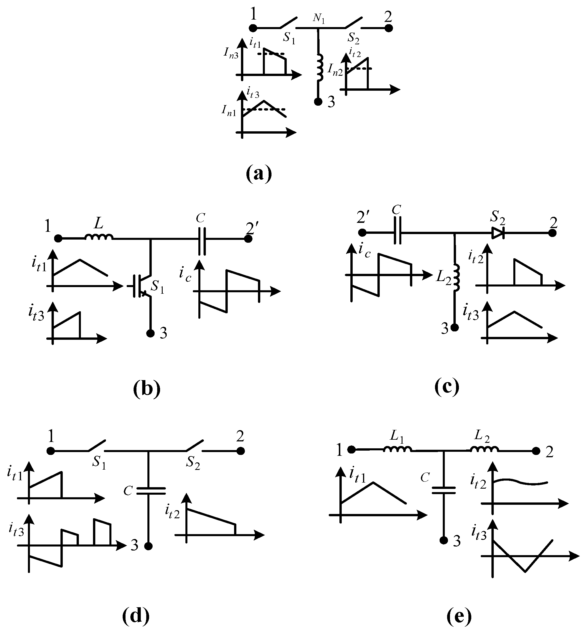
The BBBs presented in [33] are illustrated in Figure 1. Current waveshapes are also shown in the figure for each terminal of the listed BBB. These BBBs are able to synthesize all the converters in [28]. Moreover, the current-fed and voltage-fed full-bridge DC-DC converters can also be synthesized using the same BBBs. As such, the use of BBBs provides more flexibility in the synthesis of converters. As stated in Section 1, not all the synthesized converters find common use in practical applications. It is from this consideration that this paper limits the number of converters to those that find common use in practical applications. Converters considered in this study are listed in Table 1 with known merits. The synthesis of these converters only requires Type 1, Type 2, and the filter block as a BBB, i.e., a Type 3 BBB will not be used. It should be noted that the filter block does not need to be an LCL filter; an LCL filter is shown to signify the highest level of filtering. Thus, an L, C, LC, or CL filter can also represent the filter block in Figure 1e. To synthesize a practical converter, the following conditions apply for any of the BBBs in Figure 1:
  • All the terminal currents of the BBB should be DC, if it is to be used independently to synthesize a converter.
  • A BBB has distinct operating modes for the switching elements in order to ensure proper operation.
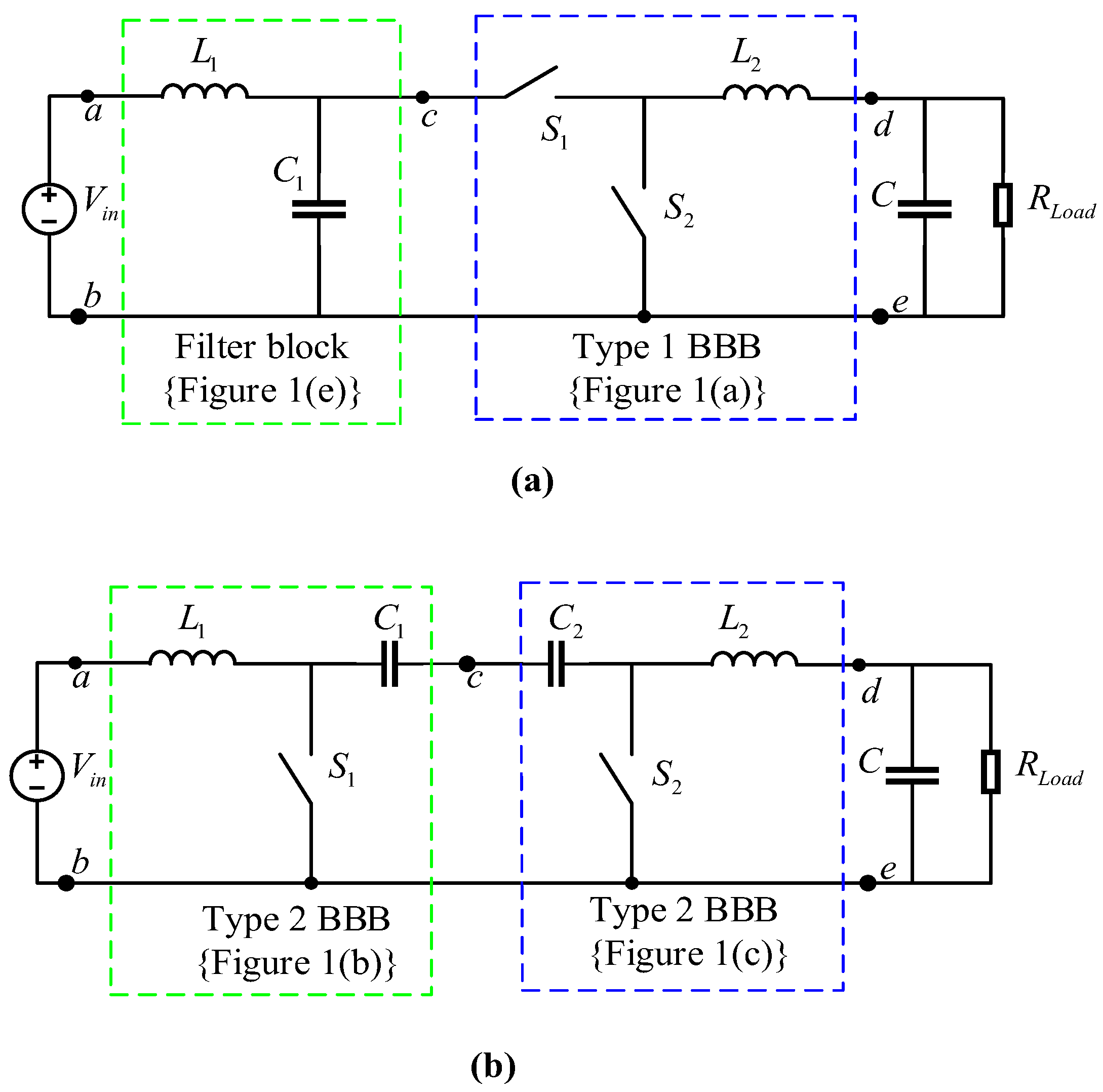
Considering the conditions listed above, only Type 1 BBBs can be used alone to realize a practical converter. An example of a converter derived from this BBB will be the conventional buck converter. Since this BBB type is identical to converter cell A in [28], the other two converters that can be synthesized from Type 1 BBBs will be the conventional boost converter and conventional buck-boost converter. A Type 2 BBB needs to be combined with other BBBs in order to realize a practical DC-DC converter. The filter block is a complementary block, in that it always has to be connected to a BBB which can independently realise a practical converter, e.g., a Type 1 BBB. BBBs can be connected in a cascade, stacked, paralled/interleaved, or differential connection. A cascade connection of BBBs is sufficient to synthesize all the converters in Table 1. A circuit-based example on the synthesis of two of the converters considered in this study is shown in Figure 2. A cascade connection of a Type 1 BBB and the filter block synthesizes the buck converter with an input filter. On the other hand, a cascade connection of two Type 2 BBBs synthesizes the Cuk converter.
3. Modelling Concept Development

3.1. Modelling Generalised Circuit

To highlight the main idea behind the proposed modelling scheme, first consider the generalized circuit diagram shown in Figure 3. Any non-isolated converter given in Table 1 can be described as a cascade connection of BBBs sandwiched between the input-port and the output-port. The input-port is typically connected to a DC source. A resistor is connected in series with the source to model internal losses of the source. For an ideal source, this resistance will be zero (i.e., R g = 0   ). The output-port constitutes a parallel connection of a capacitor and a load resistor. The load resistor represents the total active power delivered to the load and the capacitance represents voltage filtering necessary to suppress ripples in the output voltage. The equivalent series resistance of the capacitor is represented with a resistor r C to model the non-ideal parameters of the capacitor.
Once the main components of the generalized circuit diagram in Figure 3 are well defined, the modelling procedure will be illustrated considering the two BBBs making up the converter. Each BBB’s steady-state behavior, or the small-signal behavior, can be independently modelled using the circuit averaging modelling scheme. For the purpose of this paper, both steady-state and small-signal models are of interest. The circuit averaging modelling scheme is employed because it retains the graphical representation of the BBB’s circuit components and proves to be more intuitive for this section of the paper. The resultant equivalent circuit will then be considered as a two-port network, the parameters of choice will be dictated by the BBB’s connection in the network making up a specified circuit. Merits and demerits of two-port parameters based on circuit connection are fully captured in the available literature [38,47].
Since the most prominent BBB connection in the synthesis of converters in Table 1 is the ‘cascade’ connection, transmission parameters will be more suited to describe the BBB as a two-port network. As such, each of the BBBs making up the converter in Figure 3 can have their small-signal dynamics and steady-state behavior represented as shown in (1a) and (1b), respectively. To distinguish the input side BBB’s transmission parameters from those of the output side BBB, superscripts ‘i’ and ‘o’ will be used to denote input and output, respectively. Using this notation, (2a) and (2b) will, respectively, denote small-signal and steady-state transmission parameters for the input side BBB, while (3a) and (3b) represent small-signal and steady state transmission parameters for the output side BBB, respectively.
[ v ˜ 1 ( s ) ι ˜ 1 ( s ) ] = [ A ( s ) B ( s ) C ( s ) D ( s ) ] [ v ˜ 2 ( s ) ι ˜ 2 ( s ) ] + [ v ˜ i n d T ( s ) ι ˜ i n d T ( s ) ] δ ˜ ( s )
where:
  • v ˜ 1 ( s ) AC input voltage of a given BBB
  • ι ˜ 1 ( s ) AC input current of a given BBB
  • v ˜ 2 ( s ) AC output voltage of a given BBB
  • ι ˜ 2 ( s ) AC output current of a given BBB
  • v ˜ i n d T ( s ) AC input voltage of a given BBB due to the presence of independent sources for transmission parameters
  • ι ˜ i n d T ( s ) AC input current of a given BBB due to the presence of independent sources for transmission parameters
  • δ ˜ ( s ) AC excursions of the active switch duty ratio
[ V 1 I 1 ] = [ A B C D ] [ V 2 I 2 ] + [ V i n d T I i n d T ]
[ v ˜ 1 ( i ) ( s ) ι ˜ 1 ( i ) ( s ) ] = [ A ( i ) ( s ) B ( i ) ( s ) C ( i ) ( s ) D ( i ) ( s ) ] [ v ˜ 2 ( i ) ( s ) ι ˜ 2 ( i ) ( s ) ] + [ v ˜ i n d T ( i ) ( s ) ι ˜ i n d T ( i ) ( s ) ] δ ˜ ( s )
[ V 1 i I 1 i ] = [ A ( i ) B ( i ) C ( i ) D ( i ) ] [ V 2 i I 2 i ] + [ V i n d T ( i ) I i n d T ( i ) ]
[ v ˜ 1 ( o ) ( s ) ι ˜ 1 ( o ) ( s ) ] = [ A ( o ) ( s ) B ( o ) ( s ) C ( o ) ( s ) D ( o ) ( s ) ] [ v ˜ 2 ( o ) ( s ) ι ˜ 2 ( o ) ( s ) ] + [ v ˜ i n d T ( o ) ( s ) ι ˜ i n d T ( o ) ( s ) ] δ ˜ ( s )
[ V 1 o I 1 o ] = [ A ( o ) B ( o ) C ( o ) D ( o ) ] [ V 2 o I 2 o ] + [ V i n d T ( o ) I i n d T ( o ) ]
From Figure 3, it can be proved that the input voltage and current of the input BBB are the same as the converter’s input voltage and current (4a), and the output voltage and current of the output BBB are the same as the converter’s output voltage and current (4b). Additionally, it can also be proved that the output voltage and current of the input BBB are the same as the input voltage and current of the output BBB for small-signal analysis (5a) and steady-state (5b), from which (6a) and (6b) are the resultants. Equation (6a, b) represents the generalized network of Figure 3 as a two-port network based on transmission parameters. These equations are sufficient for deriving both small-signal and steady-state models of the generalized network.
[ v ˜ 1 ( i ) ( s ) ι ˜ 1 ( i ) ( s ) ] [ v ˜ i n ( s ) ι ˜ i n ( s ) ]
[ v ˜ 2 ( o ) ( s ) ι ˜ 2 ( o ) ( s ) ] [ v ˜ o u t ( s ) ι ˜ o u t ( s ) ]
[ v ˜ 2 ( i ) ( s ) ι ˜ 2 ( i ) ( s ) ] = [ v ˜ 1 ( o ) ( s ) ι ˜ 1 ( o ) ( s ) ]
[ V 2 i I 2 i ] = [ V 1 o I 1 o ]
[ v ˜ i n ( s ) ι ˜ i n ( s ) ] = [ A ( s ) B ( s ) C ( s ) D ( s ) ] [ v ˜ o u t ( s ) ι ˜ o u t ( s ) ] + [ v ˜ i n d T ( s ) ι ˜ i n d T ( s ) ] δ ˜ ( s )
where:
  • A ( s ) = A ( i ) ( s ) A ( o ) ( s ) + B ( i ) ( s ) C ( o ) ( s )
  • ( s ) = A ( i ) ( s ) B ( o ) ( s ) + B ( i ) ( s ) D ( o ) ( s )
  • C ( s ) = C ( i ) ( s ) A ( o ) ( s ) + D ( i ) ( s ) C ( o ) ( s )
  • D ( s ) = C ( i ) ( s ) B ( o ) ( s ) + D ( i ) ( s ) D ( o ) ( s )
  • v ˜ i n d T ( s ) = { A ( i ) ( s ) v ˜ i n d T ( o ) ( s ) + B ( i ) ( s ) ι ˜ i n d T ( o ) ( s ) } + v ˜ i n d T ( i ) ( s )
  • ι ˜ i n d T ( s ) = { C ( i ) ( s ) v ˜ i n d T ( o ) ( s ) + D ( i ) ( s ) ι ˜ i n d T ( o ) ( s ) } + ι ˜ i n d T ( i ) ( s )
[ V i n I i n ] = [ A B C D ] [ V o u t I o u t ] + [ V i n d T I i n d T ]
where:
  • A = A ( i ) A ( o ) + B ( i ) C ( o )
  • B = A ( i ) B ( o ) + B ( i ) D ( o )
  • C = C ( i ) A ( o ) + D ( i ) C ( o )
  • D = C ( i ) B ( o ) + D ( i ) D ( o )
  • V i n d T = { A ( i ) V i n d ( o ) + B ( i ) I i n d ( o ) } + V i n d ( i )
  • I i n d T = { C ( i ) V i n d ( o ) + D ( i ) I i n d ( o ) } + I i n d ( i )
v ˜ 2 ( o ) ( s ) = ι ˜ 2 ( o ) ( s ) Z L o a d ( s )
V 2 o = I 2 o Z L o a d
Z L o a d ( s ) = R L Z C ( s ) R L + Z C ( s )

Generalised Power Stage Models

The small-signal models of interest will be the audio-susceptibility transfer function (8), the control-to-output voltage transfer function (9), input impedance (10), and output impedance (11). The steady-state model will mainly constitute the voltage gain (12). All the models represented by (8)–(12) are independent of the converter topology, and thus generalizes the modelling procedure when the coefficients of the matrices in (6a) and (6b) are known.
v ˜ o u t ( s ) v ˜ i n ( s ) | δ ˜ ( s ) = 0 = Z L o a d ( s ) A ( s ) Z L o a d ( s ) + B ( s )
v ˜ o u t ( s ) δ ˜ ( s ) | v ˜ i n ( s ) = 0 = v ˜ i n d T ( s ) Z L o a d ( s ) A ( s ) Z L o a d ( s ) + B ( s )
Z i n ( s ) = v ˜ i n ( s ) ι ˜ i n ( s ) | δ ˜ ( s ) = 0 = A ( s ) Z L o a d ( s ) + B ( s ) C ( s ) Z L o a d ( s ) + D ( s )
Z o u t ( s ) = v ˜ o u t ( s ) ι ˜ o u t ( s ) | v ˜ i n ( s ) = 0 δ ˜ ( s ) = 0 ,   = B ( s ) Z L o a d ( s ) A ( s ) Z L o a d ( s ) + B ( s )
V o u t V i n | V i n d = I i n d = 0 = z L o a d Z L o a d A + B

3.2. Modellling Type 1 BBBs

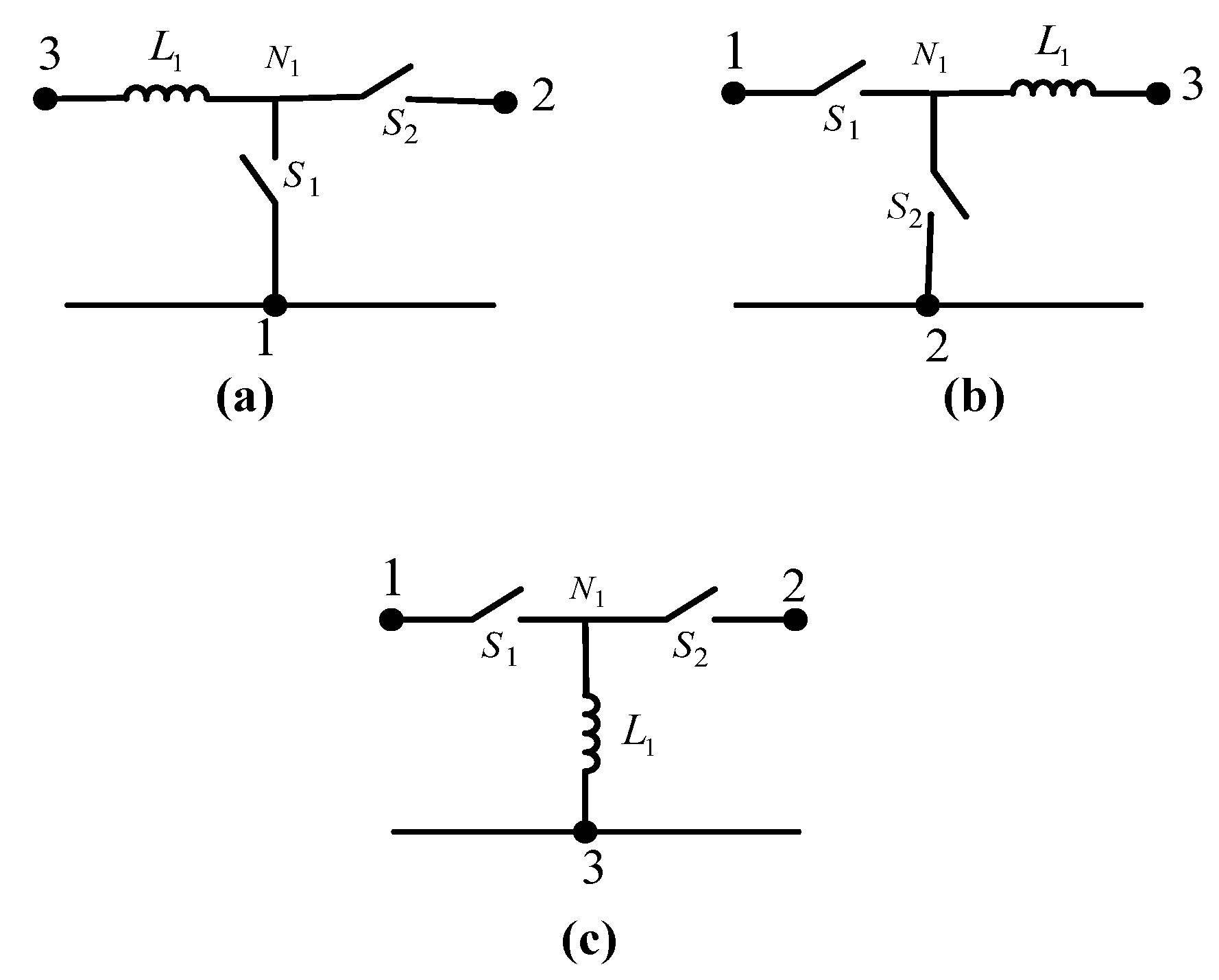
Type 1 BBBs appear in various connection forms in relation to the input and output ports. Consider Figure 1a, node 1 can be connected to the common rail, making port 2-1 and 3-1 input and output ports, respectively. On the other hand, node 2 can be connected to the common rail, making port 1-2 and 3-2 input and output ports, respectively. More configurations of this BBB can be deduced from the converters listed in Table 1. These configurations are a direct result of the converter synthesis process discussed in [28] based on canonical cell permutations. As such, the uniqueness of a two-port model description of this BBB, based on the circuit averaging modelling technique, is dictated by port definition. Possible port definitions for this BBB are listed in Figure 4. Although numerous port definitions exist, the resultant circuit models are equivalent [48]. It will later be shown that the resultant models of all permissible port definitions can actually be generalized.

3.2.1. Ideal Model

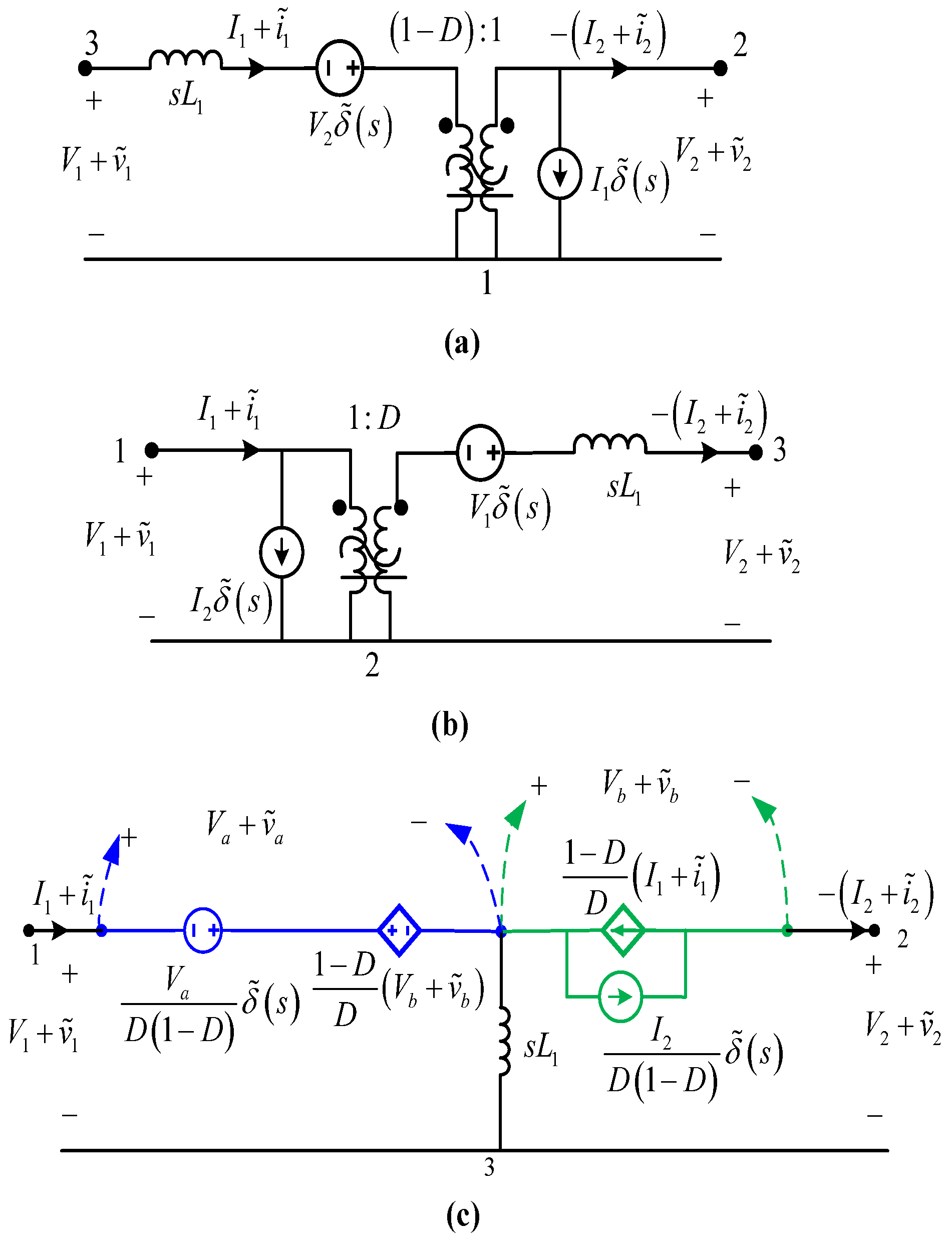
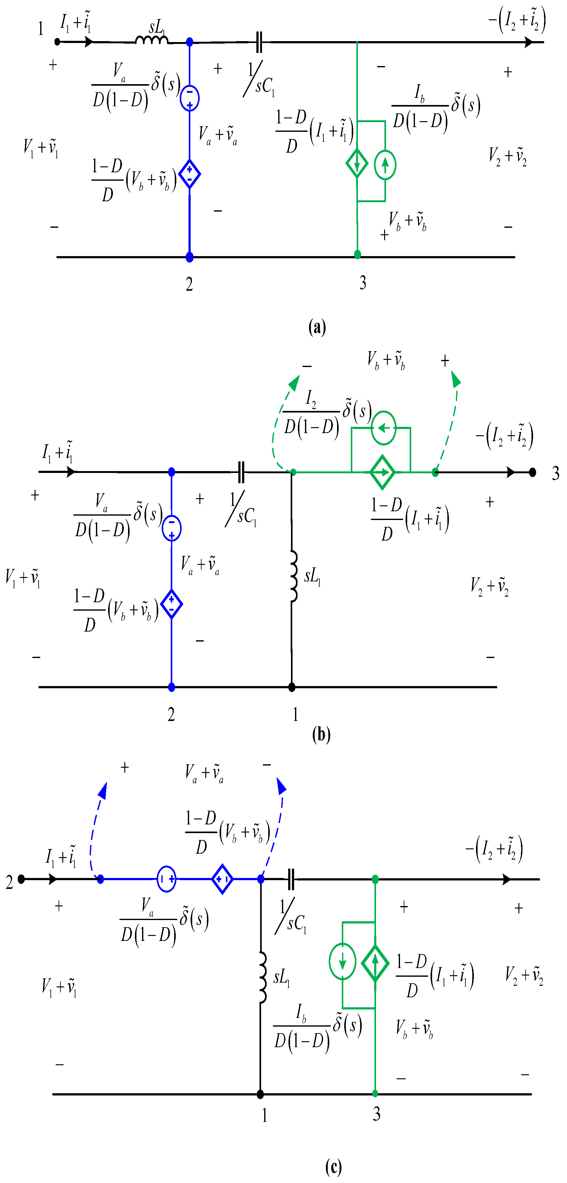
In this section, lossless equivalent circuits for computing small-signal and steady-state models for the BBBs in Figure 4a–c are presented in Figure 5a–c, following the circuit averaging modelling approach. In Figure 5c, the switch and diode averaged circuits are shown in blue and green with a terminal voltage V a + v ˜ a and V b + v ˜ b , respectively. The equivalent circuits of the BBBs shown in Figure 5a–c are considered to be two-port networks, and the corresponding coefficients of the small-signal Equation (1a) are shown in Table 2. In a similar manner, the coefficients of the steady-state Equation (1b) are also shown in Table 2.

3.2.2. Non-Ideal Model

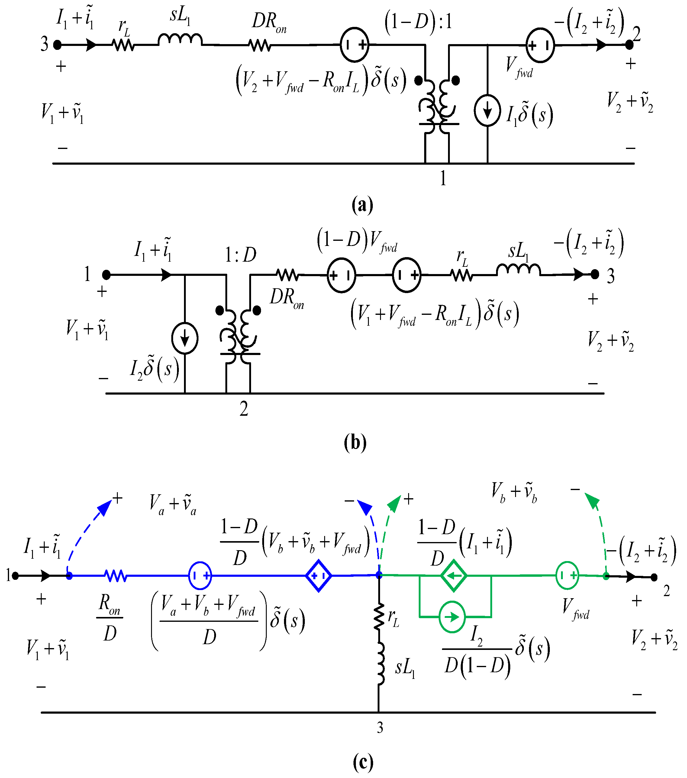
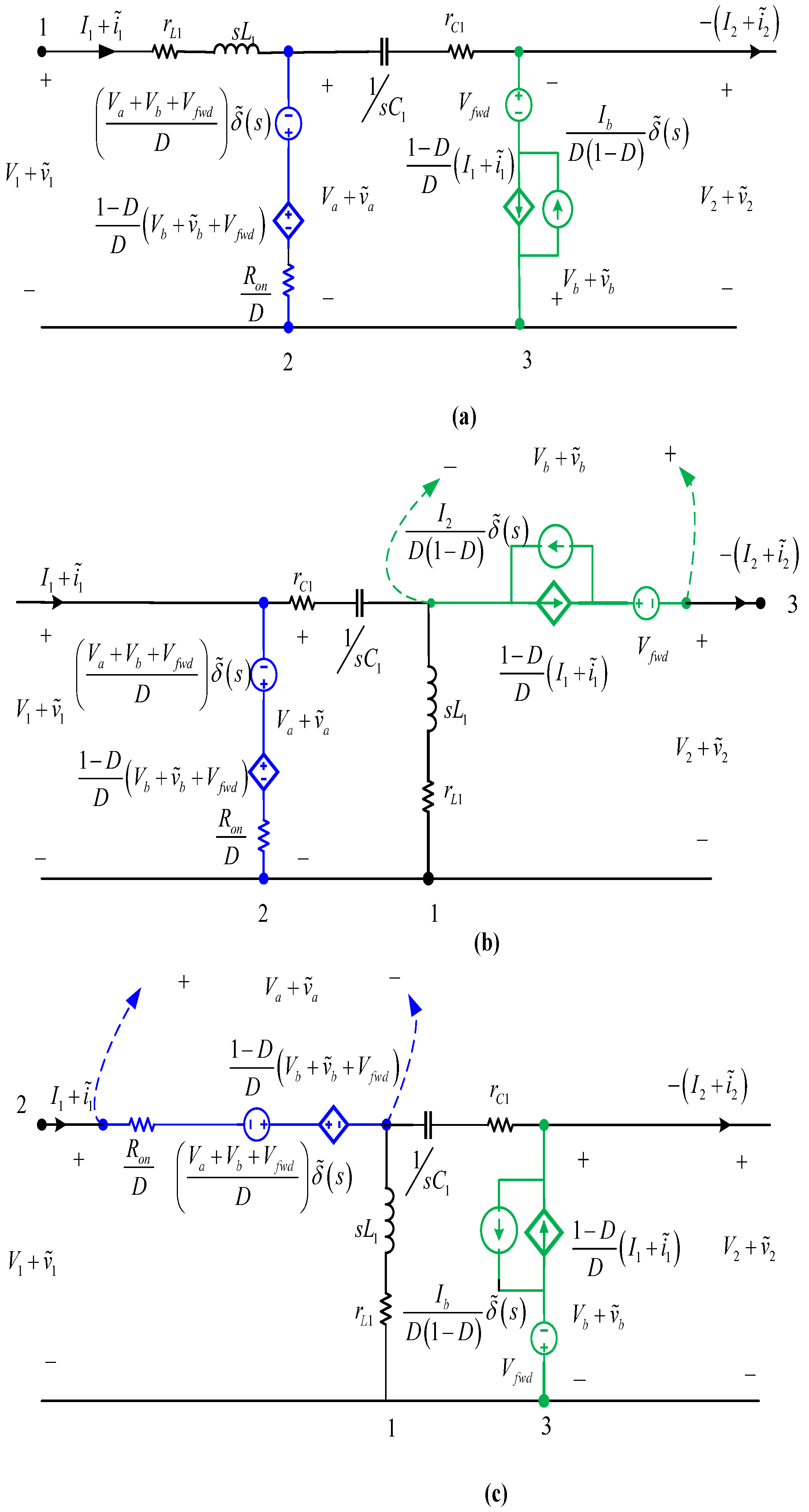
In this section, more practical equivalent circuits for computing small-signal and steady-state models for the BBBs in Figure 4a–c are presented in Figure 6a–c, following the circuit averaging modelling approach. These equivalent circuits consider the active switch’s resistance ‘ R o n ’, diode forward voltage ‘ V f w d ’, capacitor series resistance ‘ r C ’, and inductor series resistance ‘ r L ’ as non-ideal parameters of the circuit. The equivalent circuits shown in Figure 6a–c are considered as two-port networks, and the corresponding coefficients of the small-signal Equation (1a) are shown in Table 2. In a similar manner, the coefficients of the steady-state Equation (1b) are also shown in Table 2.

3.2.3. Generalised Type 1 Model

The Type 1 BBB is sufficient to independently derive the three conventional converters, i.e., boost, buck, and buck-boost DC-DC converters. These converters are well-known and describe the basic DC-DC converter functionalities, i.e., voltage step-up (13), voltage step-down (14), and voltage step-up and step-down (15). Equations (13)–(15) can be generalized with two functions, one describing the numerator and the other describing the denominator, as shown in (16). It should be noted that the non-ideal model is the most general model between the two models presented for each rail connection in Table 2. Thus, the ideal model can be derived directly from the non-ideal model when all the non-ideal parameters are set to zero. For the sake of expediency in the generalization process for this BBB Type, the matrix describing the two-port network, in the absence of perturbations in the control variable, can be generalized, as shown in (17). Such a generalization is independent of rail connection and enables one to describe the equivalent two-port model for Type 1 BBBs by inspection. It should be noted that (17) represents the two-port model of any Type 1 BBB, regardless of whether it is an input or output BBB. As such, if the converter of interest is one of the conventional converters, then the audio-susceptibility transfer function can also be generalized or equivalently computed by inspection, as shown in (18). The sign of the matrix entries in (17) is negative if there is a polarity inversion of the input voltage on the output side.
V o u t V i n = 1 1 D
V o u t V i n = D
V o u t V i n = D 1 D
V o u t V i n = f ( D ) g ( D )
[ v ˜ 1 ( s ) ι ˜ 1 ( s ) ] = ± [ g ( D ) f ( D ) Z T f ( D ) g ( D ) 0 f ( D ) g ( D ) ] [ v ˜ 2 ( s ) ι ˜ 2 ( s ) ]
where: Z T = D R o n + Z L ; Z L = s L 1 + r L
v ˜ o u t ( s ) v ˜ i n ( s ) | δ ˜ ( s ) = 0 = Z L o a d ( s ) g ( D ) f ( D ) Z L o a d ( s ) + Z T f ( D ) g ( D )

3.3. Modelling Type 2 BBB

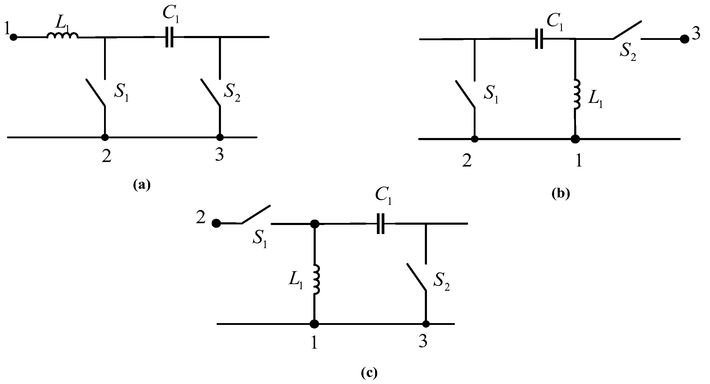
Similarly, the Type 2 BBB also appears in various connection forms in relation to the input and output ports. As such, possible combinations of this BBB will be considered in the same manner as the Type 1 BBB. It can be seen that Type 2 BBBs, as presented in [33], contain one semiconductor device, i.e., it contains either a diode or an active switch. In a practical converter, for each active switch there is a complementary diode. As such, it can be expected that a practical converter based on Type 2 BBBs must have at least two Type 2 BBBs. This observation was also made in [33] based on terminal current signals. It was observed that not all the terminal currents of this building block are DC, which rendered the BBB unsuitable to independently realize a practical converter. Thus, it has to be configured with other BBBs to realise a practical converter. It follows that unlike current signal waveshapes which can be independently deduced from each BBB regardless of the number of switching elements or nature of the terminal currents, power stage small-signal models cannot be derived independently. This is the case because average switch models for switching devices are modelled with dependent sources, which means sources are controlled by circuit variables. Thus, the dependent voltage source used to model the active switch has controlling variables which depend on the diode variables, and vice-versa. If either of the Type 2 BBBs were to be considered in isolation, there will always be a variable which cannot be represented in terms of port variables, and thus it is impossible to conform to the two-port model. To deal with this, a minimum structure which is inclusive of both switches is considered, this can be considered a lumped form of Type 2 BBBs. Figure 7 shows different rail connection configurations for the introduced lumped form of Type 2 BBBs. This lumped block only needs to be combined with a filter block to form a practical converter. Practical converters made up of the lumped form of Type 2 BBBs include the Cuk, Sepic, and Zeta converters. As such, the lumped BBBs would suggest that there are close ties in the derivation of the Cuk and group G converters, i.e., Sepic and Zeta. This is different from the work presented in [28], wherein these converters were classified as belonging to separate converter cells.

3.3.1. Ideal Model

In this section, lossless equivalent circuits for computing small-signal and steady-state models for the BBBs in Figure 7a–c are presented in Figure 8a–c, following the circuit averaging modelling approach. The equivalent circuits of the BBBs shown in Figure 8a–c are considered as two-port networks, and the corresponding coefficients of the small-signal Equation (1a) are shown in Table 3. In a similar manner, the coefficients of the steady-state Equation (1b) are also shown in Table 3.

3.3.2. Non-Ideal Model

In this section, more practical equivalent circuits for computing small-signal and steady-state models for the BBBs in Figure 7a–c are presented in Figure 9a–c, following the circuit averaging modelling approach. These equivalent circuits consider the active switch’s resistance ‘ R o n ’, diode forward voltage ‘ V f w d ’, capacitor series resistance ‘ r C ’,and inductor series resistance ‘ r L ’ as non-ideal parameters of the circuit. The equivalent circuits shown in Figure 9a–c are considered as two-port networks, and the corresponding coefficients of the small-signal Equation (1a) are shown in Table 3. In a similar manner, the coefficients of the steady-state Equation (1b) are also shown in Table 3.

3.4. Modelling the Filter Block

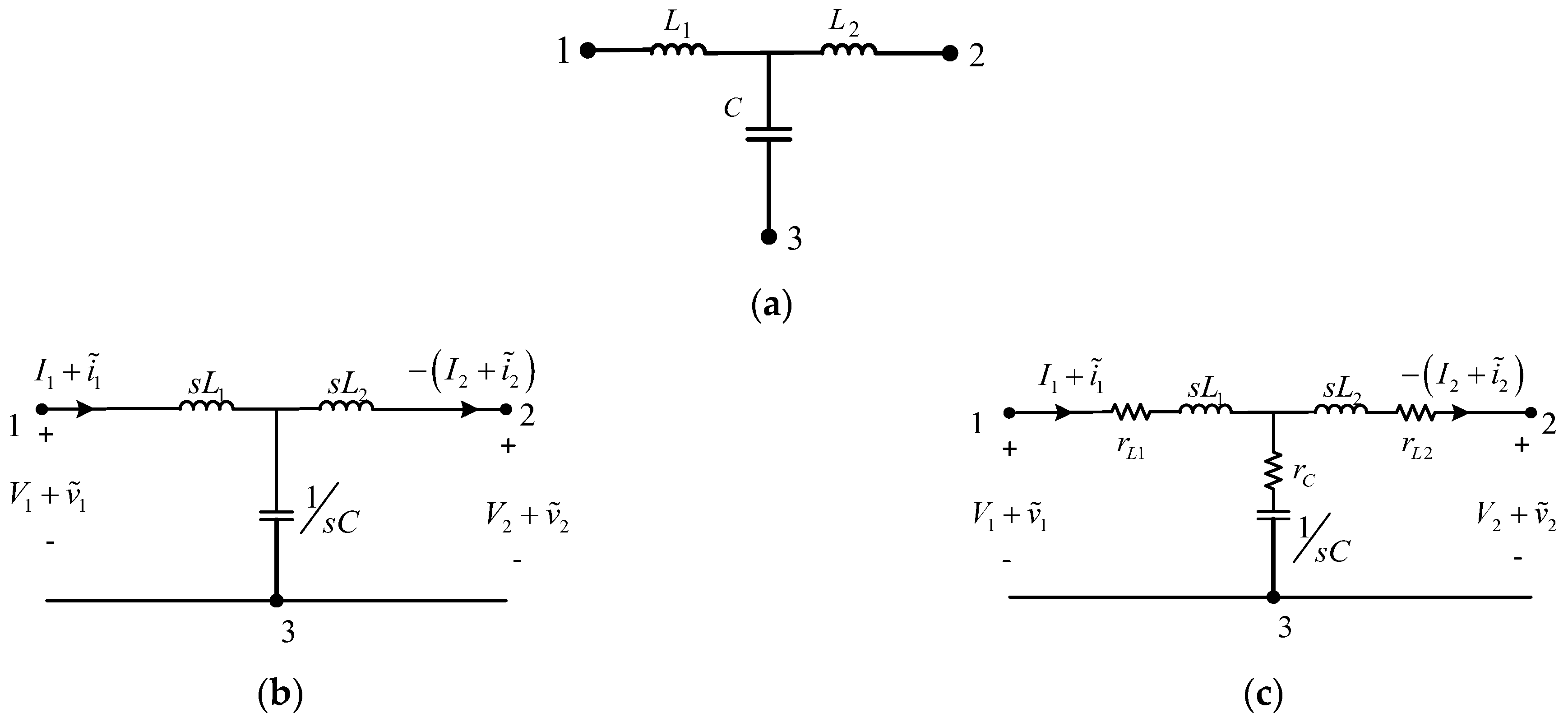
Finally, as mentioned in Section 2, the filter block has an LCL filter as the most generic form of the BBBs. This represents the highest level of filtering. To compute the power stage model of this BBB, the generic form is considered, i.e., an LCL filter. It will also be shown that models for any other form of the filter block (i.e., LC, CL, L. or C) can be computed by simply setting the LCL filter elements not present in a given configuration to zero, e.g., for an LC filter, one of the inductances which appear in the LCL filter circuit model will be set to zero since it does not appear in the LC filter circuit model. Additionally, this BBB does not contain any switching components. As such, modelling this BBB is relatively easy. Figure 1e shows the circuit model of the filter BBB. The approach to model the LCL filter results in a generalised model for the filter block. Thus, substantially reducing modelling effort for any possible filter configuration.

3.4.1. Ideal Model

In this section, a lossless equivalent circuit for computing small-signal and steady-state models for the filter block in Figure 10a is presented in Figure 10b. Since the filter block is entirely made up of linear elements, it is an inherently linear system. As such, the circuit averaging modelling approach is not necessary for this BBB. The equivalent circuit of the BBB shown in Figure 10b is considered as a two-port network, and the corresponding coefficients of the small-signal Equation (1a) are shown in Table 4. In a similar manner, the coefficients of the steady-state Equation (1b) are also shown in Table 4.

3.4.2. Non-Ideal Model

In this section, a more practical equivalent circuit for computing small-signal and steady-state models for the filter block is presented in Figure 10c. As mentioned earlier, the filter block is made up entirely of linear elements. Thus, the modelling does not require specialised modelling techniques such as the circuit averaging modelling technique. This equivalent circuit considers the capacitor series resistance ‘ r C ’ and inductor series resistance ‘ r L ’ as non-ideal parameters of the circuit. The equivalent circuit shown in Figure 10c is considered as a two-port network, and the corresponding coefficients of the small-signal Equation (1a) are shown in Table 4. In a similar manner, the coefficients of the steady-state Equation (1b) are also shown in Table 4.

4. Non-Conventional Converters

In this section, the modularity of the proposed modelling scheme is extended to non-conventional converters. For this purpose, the voltage-fed and current-fed full-bridge DC-DC converters are considered. The modelling procedure is still oriented on the synthesis of the circuit of interest based on BBBs modelled as two-port networks. As such, the BBBs and the accompanying connection ought to be clearly defined. It should be noted that the same two-port network can be modelled using different, yet equivalent, parameters. The choice to use transmission parameters was based on the observations made in Section 3, i.e., all the converters considered in this study, as captured in Table 1, can be synthesized based on a cascade connection of BBBs. Thus, validating the choice to use transmission parameters. As mentioned in Section 3, there are well-known merits and demerits for using specified two-port network parameters based on the circuit configuration.

4.1. Shunt-Series Connection of BBBs

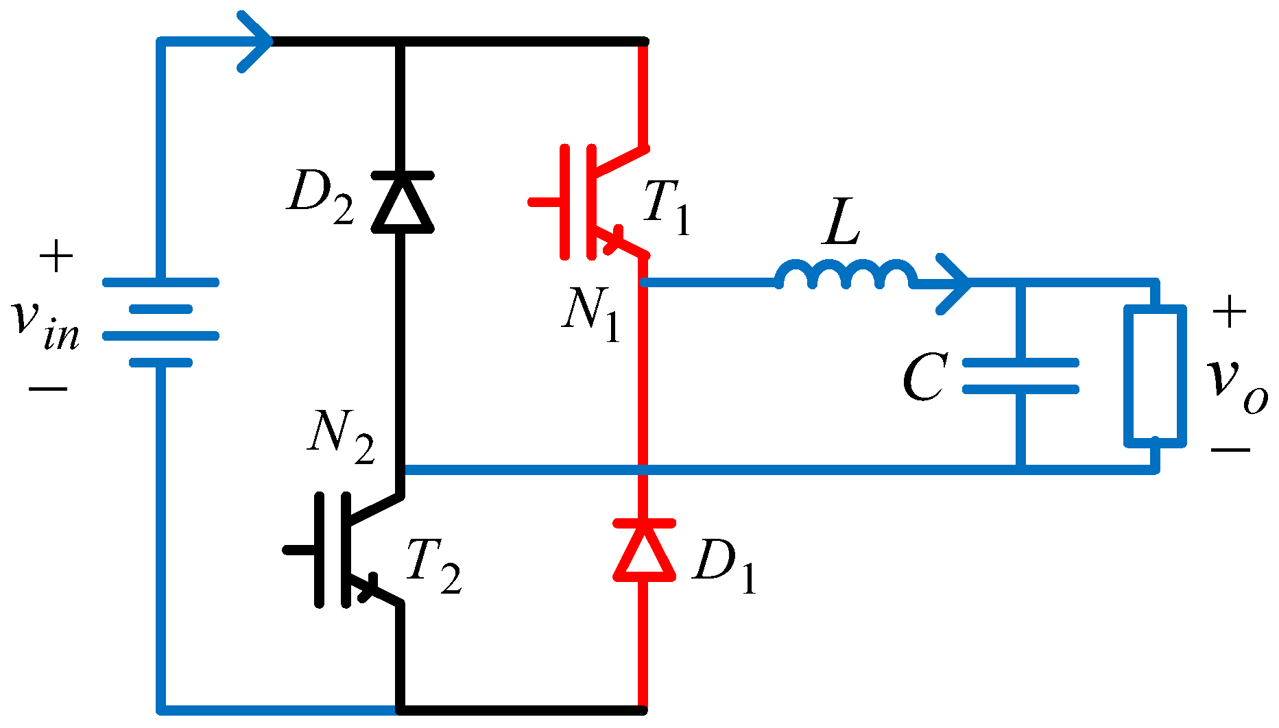
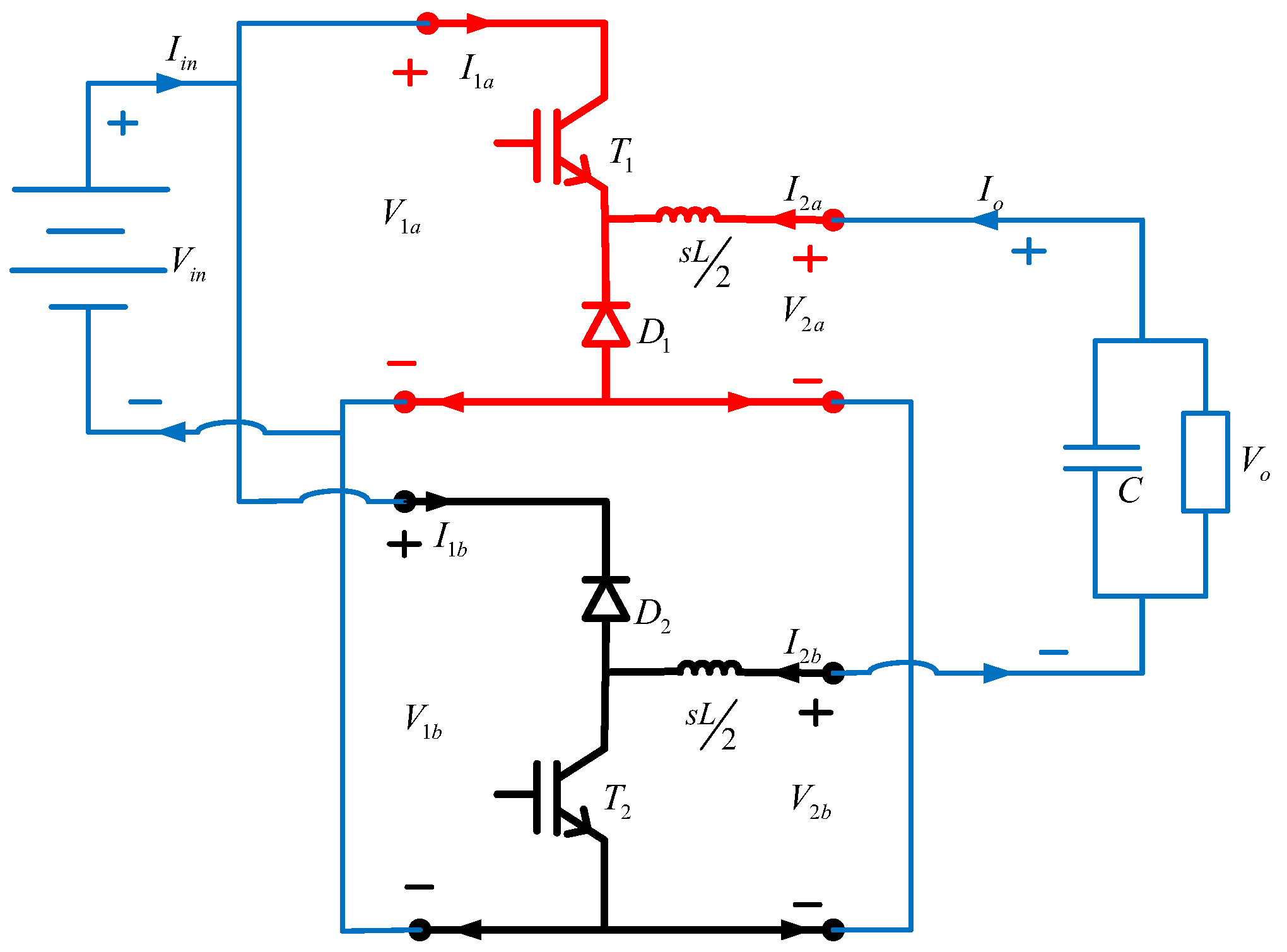
The voltage-fed full-bridge DC-DC converter circuit diagram can be construed as an input-shunt, output-series connection of Type 1 BBBs. Figure 11 shows a circuit diagram of this topology. Additionally, Figure 12 shows the same circuit with a refined depiction of the BBB connections. It can be seen from the two figures that there are two Type 1 BBBs, one shown with red lines and the other with black lines. Two-port network models of Type 1 BBBs are captured in Table 2. Moreover, equivalent network parameters of Type 1 BBBs can easily be computed from predefined matrices in the available literature [38,47]. For example, given transmission parameters of a Type 1 BBB, the equivalent g-parameters can be derived, as shown in (19). A complete table for computing equivalent two-port parameters in the absence of perturbations in the duty ratio is given in [47]. For our circuit of interest, it can be shown that the g-parameters are more suited for modelling a shunt-series connected circuit.
[ ι ˜ 1 ( s ) v ˜ 2 ( s ) ] = [ C ( s ) A ( s ) d e t ( T ) A ( s ) 1 A ( s ) B ( s ) A ( s ) ] [ v ˜ 1 ( s ) ι ˜ 2 ( s ) ] + [ A ( s ) ι ˜ i n d T ( s ) C ( s ) v ˜ i n d T ( s ) A ( s ) v ˜ i n d T ( s ) A ( s ) ] δ ˜ ( s )
where:   d e t ( T ) = A ( s ) D ( s ) B ( s ) C ( s )
For any input-shunt, output-series connected topology, the g-parameter based two-port model in (20) is always valid. It can be seen from (20) that the input current is a sum of the input currents of the BBBs and the output voltage is a sum of the output BBB voltages. In (20), superscripts ‘u’ and ‘l’ are used to distinguish parameters associated with the upper (red) BBB from those associated with the lower (black) BBB.
[ ι ˜ 1 ( s ) v ˜ 2 ( s ) ] = [ ι ˜ 1 ( u ) ( s ) v ˜ 2 ( u ) ( s ) ] + [ ι ˜ 1 ( l ) ( s ) v ˜ 2 ( l ) ( s ) ]
For our circuit of interest in Figure 12 the BBB in red makes up the first BBB and has matrix entries with superscripts ‘u’, as shown in (21). On the other hand, the BBB in black makes up the second BBB and has matrix entries with superscripts ‘l’, as shown in (22). The voltages making up the series’ connected output port have different polarities in relation to the main output terminals. The polarity of the BBB in red matches the main output terminal polarity, but the polarity of the BBB in black opposes that of the main output terminals. Thus, the black BBB will contribute a negative output terminal voltage and current in relation to the main output terminals. To conform to (20), the negative sign of the terminal voltage and current of the black BBB can be entirely associated with the g-parameter matrix and the independent matrix. This only affects the off-diagonal elements of the g-parameter matrix and the second row of the independent matrix, as shown in (23).
[ ι ˜ 1 ( u ) ( s ) v ˜ 2 ( u ) ( s ) ] = [ g 11 ( u ) g 12 ( u ) g 21 ( u ) g 22 ( u ) ] [ v ˜ 1 ( u ) ( s ) ι ˜ 2 ( u ) ( s ) ] + [ ι ˜ 1 , i n d g ( u ) ( s ) v ˜ 2 , i n d g ( u ) ( s ) ] δ ˜ ( s )
[ ι ˜ 1 ( l ) ( s ) v ˜ 2 ( l ) ( s ) ] = [ g 11 ( l ) g 12 ( l ) g 21 ( l ) g 22 ( l ) ] [ v ˜ 1 ( l ) ( s ) ι ˜ 2 ( l ) ( s ) ] + [ ι ˜ 1 , i n d g ( l ) ( s ) v ˜ 2 , i n d g ( l ) ( s ) ] δ ˜ ( s )
[ ι ˜ 1 ( l ) ( s ) v ˜ 2 ( l ) ( s ) ] = [ g 11 ( l ) g 12 ( l ) g 21 ( l ) g 22 ( l ) ] [ v ˜ 1 ( l ) ( s ) ι ˜ 2 ( l ) ( s ) ] + [ ι ˜ 1 , i n d g ( l ) ( s ) v ˜ 2 , i n d g ( l ) ( s ) ] δ ˜ ( s )
Substitution of (21) and (23) into (20) yields the complete circuit model of a voltage-fed full-bridge converter (24). The corresponding steady-state model of the same circuit is shown in (25).
[ ι ˜ 1 ( s ) v ˜ 2 ( s ) ] = [ g 11 ( s ) g 12 ( s ) g 21 ( s ) g 22 ( s ) ] [ v ˜ 1 ( s ) ι ˜ 2 ( s ) ] + [ ι ˜ i n d g ( s ) v ˜ i n d g ( s ) ] δ ˜ ( s )
where:
  • g 11 ( s ) = g 11 ( u ) + g 11 ( l )
  • g 12 ( s ) = g 12 ( u ) + ( g 12 ( l ) )
  • g 21 ( s ) = g 21 ( u ) + ( g 21 ( l ) )
  • g 22 ( s ) = g 22 ( u ) + g 22 ( l )
  • ι ˜ i n d g ( s ) = ι ˜ 1 , i n d g ( u ) ( s ) + ι ˜ 1 , i n d g ( l ) ( s )
  • v ˜ i n d g ( s ) = v ˜ 2 , i n d g ( u ) ( s ) + ( v ˜ 2 , i n d g ( l ) ( s ) )
[ I 1 V 2 ] = [ g 11 g 12 g 21 g 22 ] [ V 1 I 2 ] + [ I i n d g V i n d g ]
Generalized equations for the transfer functions of interest can be directly derived from (24). Consider the control-to-output voltage transfer function, as well as the audio-susceptibility transfer function, as the transfer functions of interest. Their generalized equations, in terms of g-parameters, will be given by (26) and (27), respectively.
v ˜ o u t ( s ) δ ˜ ( s ) | v ˜ i n ( s ) = 0 = v ˜ i n d g ( s ) Z L o a d ( s ) Z L o a d ( s ) + g 22 ( s )
v ˜ o u t ( s ) v ˜ i n ( s ) | δ ˜ ( s ) = 0 = g 21 ( s ) Z L o a d ( s ) Z L o a d ( s ) + g 22 ( s )

4.2. Series-Shunt Connection of BBBs

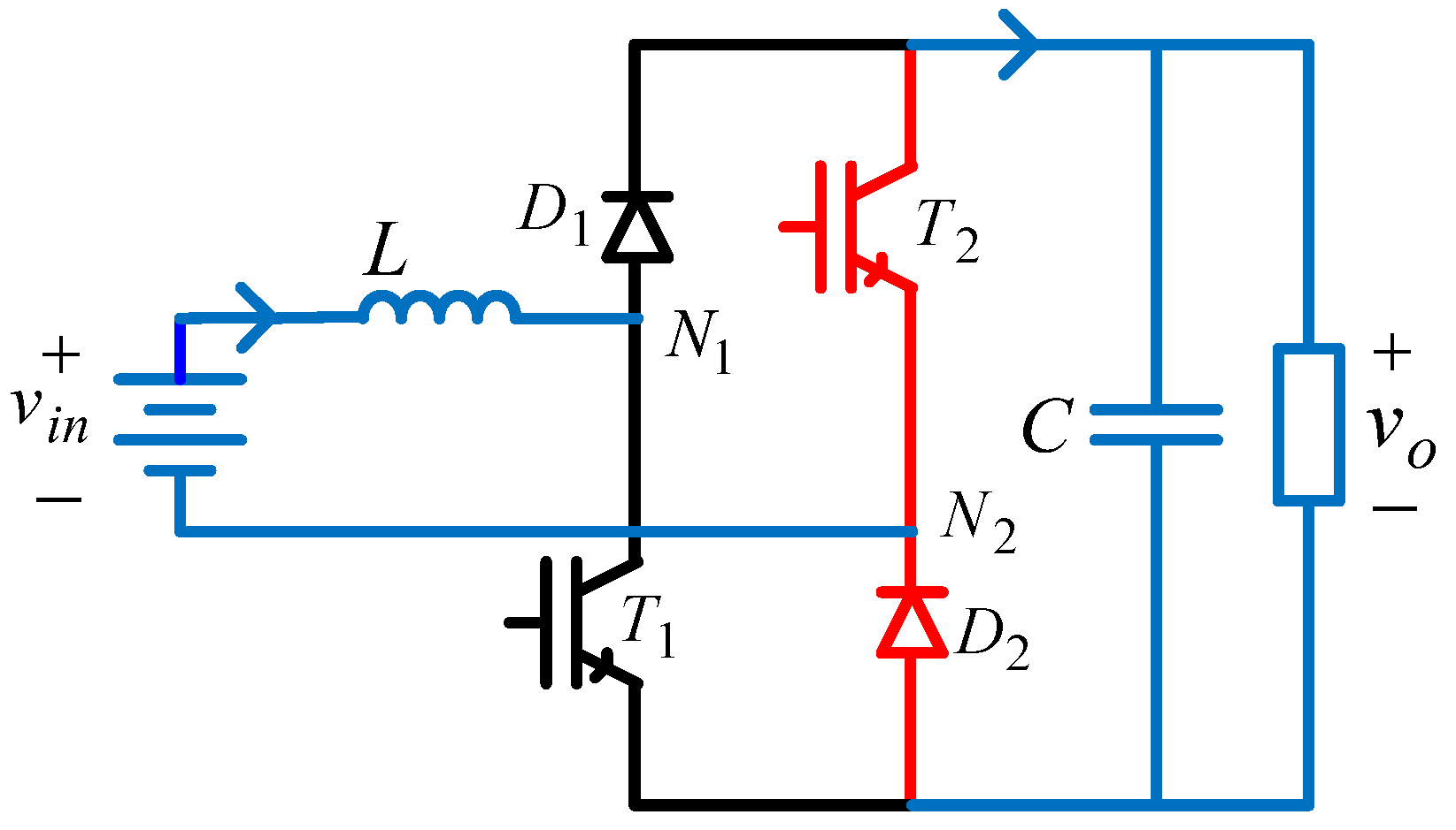
Similarly, the current-fed full-bridge DC-DC converter circuit diagram can be construed as an input-series, output-shunt connection of Type 1 BBBs. A condensed circuit diagram for this circuit topology is shown in Figure 13. It can be seen from Figure 13 that the circuit is made up of two Type 1 BBBs. It can be shown that h-parameters are more suited for modelling a series-shunt connected circuit. Thus, the transmission parameters for each BBB must be converted to h-parameters using (28). The resultant h-parameter based model of the complete circuit will assume the form of (29). It is from (29) that models of interest can be derived as generalized expressions, as shown in (30) and (31).
v ˜ 1 s ι ˜ 2 s = B s D s det T D s 1 D s C s D s ι ˜ 1 s v ˜ 2 s + D s v ˜ i n d T s B s ι ˜ i n d T s D s ι ˜ i n d T s D s δ ˜ s
[ v ˜ 1 ( s ) ι ˜ 2 ( s ) ] = [ h 11 ( s ) h 12 ( s ) h 21 ( s ) h 22 ( s ) ] [ ι ˜ 1 ( s ) v ˜ 2 ( s ) ] + [ ι ˜ i n d h ( s ) v ˜ i n d h ( s ) ] δ ˜ ( s )
v ˜ o u t ( s ) δ ˜ ( s ) | v ˜ i n ( s ) = 0 = [ h 21 ( s ) v ˜ i n d h ( s ) h 11 ( s ) ι ˜ i n d h ( s ) ] Z L o a d ( s ) Z L o a d ( s ) [ h 22 ( s ) h 11 ( s ) h 21 ( s ) h 12 ( s ) ] + h 11 ( s )
v ˜ o u t ( s ) v ˜ i n ( s ) | δ ˜ ( s ) = 0 = h 21 ( s ) Z L o a d ( s ) Z L o a d ( s ) [ h 22 ( s ) h 11 ( s ) h 21 ( s ) h 12 ( s ) ] + h 11 ( s )

5. Examples

This section seeks to validate the accuracy of the models derived using the proposed modeling scheme. Three converters from the group of converters in Table 1 are considered. Moreover, an example is also given on a non-conventional converter, discussed in Section 4. It should be noted that in any of the considered circuits, components are numbered in the direction of power flow, i.e., from left to right. From the three converters in Table 1 selected for this section, only the conventional buck-boost converter results in a second order model, the other two result in a fourth-order model. This is expected since it coincides with the number of reactive components a circuit has.
Given the range of converters considered in this study, as shown in Table 1, a total of four converters are selected for this section. Three of the selected converters represent unique combinations of BBBs, while the last one validates modularity of the proposed modelling scheme based on a non-conventional converter. The first example represents a converter made up of only Type 1 BBBs. The second example represents a converter made up of a Type 1 BBB and a filter block. The third example represents a converter made up of lumped Type 2 BBBs, and the last example represents a non-conventional converter made up of two Type 1 BBBs.

5.1. Conventional Buck-Boost Converter

5.1.1. Model Derivation

The conventional buck-boost converter can be derived from a single Type 1 BBB, whose two-port model is shown in (32). To conform to (6a), this converter can be considered as a cascade of a Type 1 BBB with a series wire, whose two-port model will be a 2 × 2 identity matrix, shown in (33). The control-to-output voltage transfer function is computed using the generalized equation shown in (9). On the other hand, the audio-susceptibility transfer function will be computed using the generalized equation in (8). Using these equations, the resultant equations for transfer functions are shown in (34) and (35).
v ˜ 1 i s ι ˜ 1 i s = 1 D D R o n D + Z L 1 D 1 D 0 D 1 D v ˜ 2 i s ι ˜ 2 i s + R o n + Z L 1 I L 1 V i n V o + V f w d 1 D D 1 D I L 1 1 D δ ˜ s
[ v ˜ 1 ( o ) ( s ) ι ˜ 1 ( o ) ( s ) ] = [ 1 0 0 1 ] [ v ˜ 2 ( o ) ( s ) ι ˜ 2 ( o ) ( s ) ] + [ 0 0 ] δ ˜ ( s )

5.1.2. Design Consideration and Comparisons

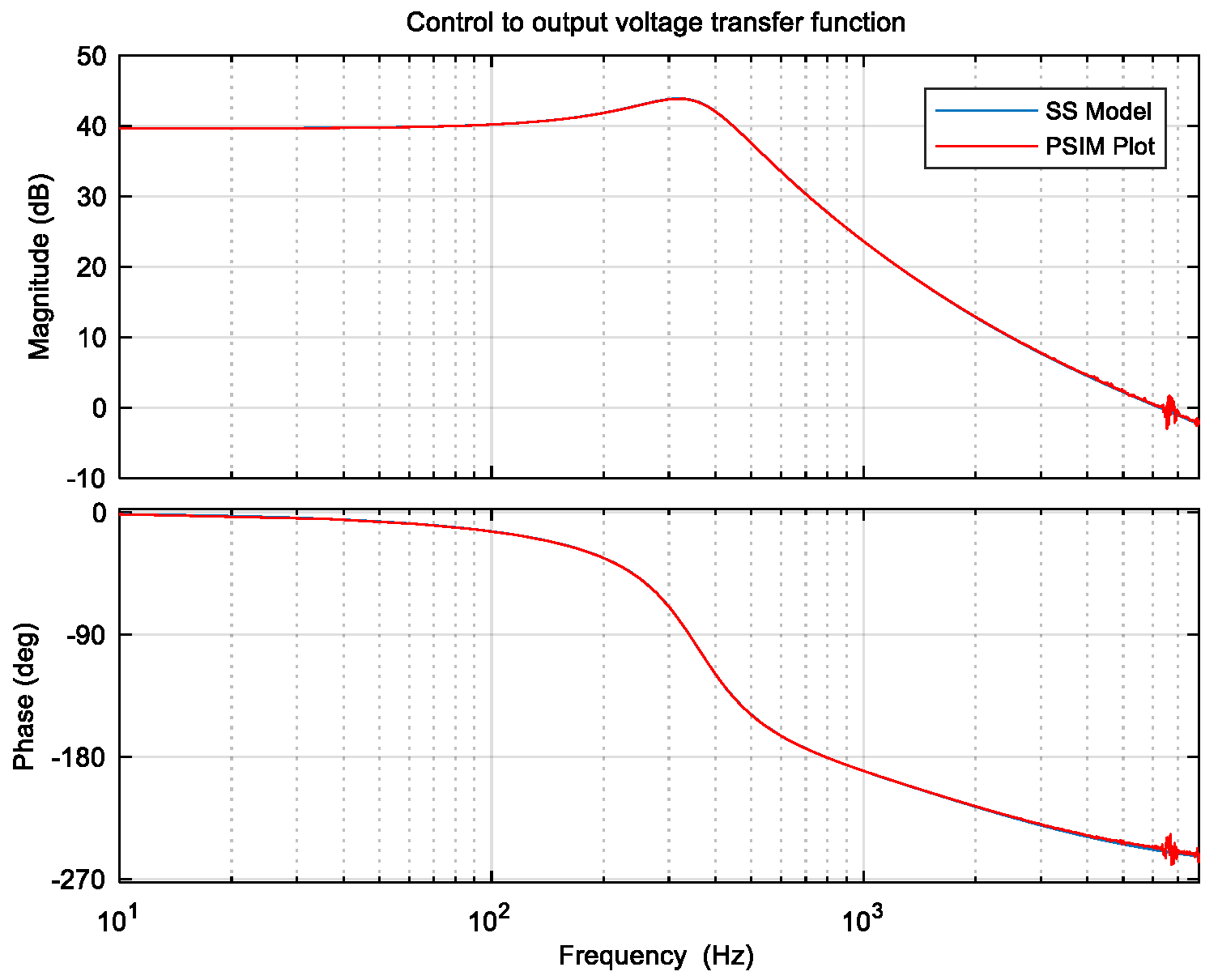
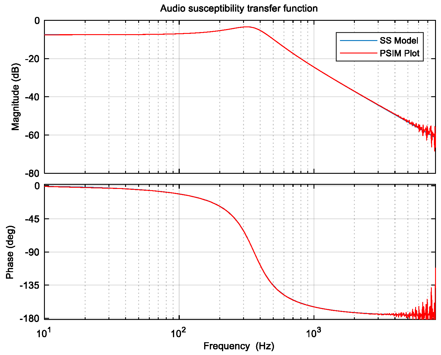
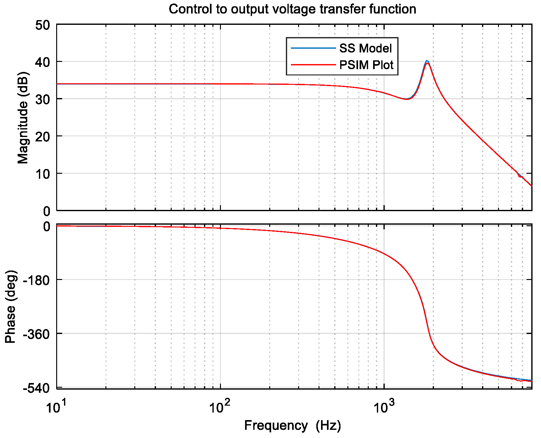
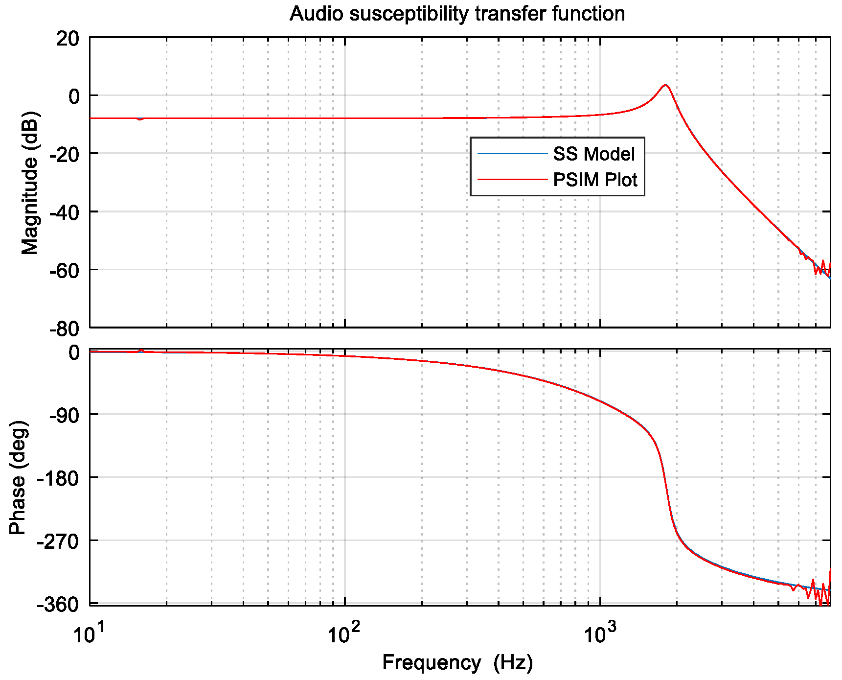
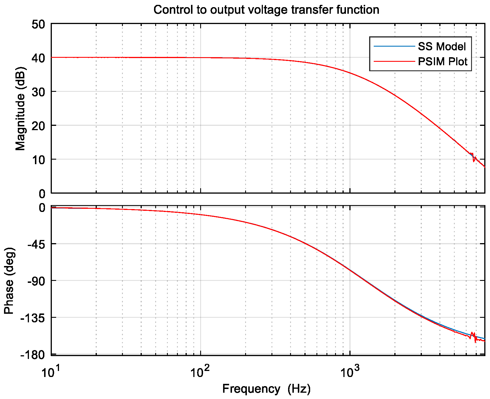
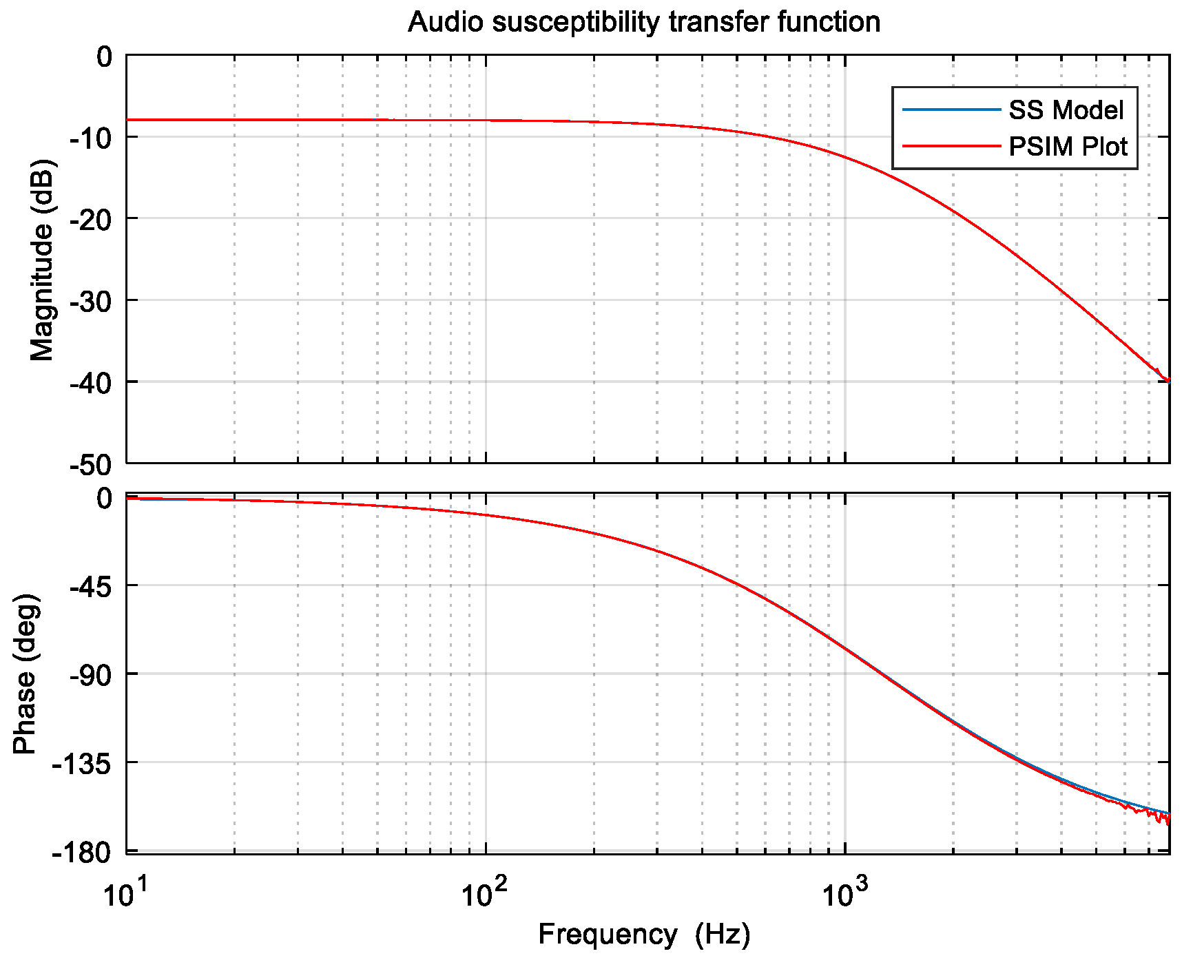
The transfer functions shown in (34) and (35) were also used to draw an equivalent Bode plot to show the complete frequency response of the system. The corresponding numerical values for the components are shown in Table 5. Moreover, the same Bode plots were independently derived using the PSim AC sweep function with the same component values in Table 5. The PSim plots and model-based plots are shown on the same set of axes for control-to-output voltage transfer function (Figure 14) and audio-susceptibility (Figure 15).
v ˜ o s δ ˜ s v ˜ i n s = 0 = r C 1 C 1 L 1 s 2 + I L 1 L 1 + I L 1 r L 1 + R o n D r C 1 C 1 1 D V i n V o + V f w d r C 1 C 1 s + I L 1 r L 1 + R o n 1 D V i n V o + V f w d C 1 L 1 + C 1 L 1 r C 1 R L s 2 + L 1 + r L 1 r C 1 C 1 R L + r C 1 C 1 1 D 2 + C 1 R o n D + r L 1 C 1 + R o n D r C 1 C 1 R L s + r L 1 + R o n D R L + 1 D 2
v ˜ o s v ˜ i n s δ ˜ s = 0 = r C 1 C 1 s D 1 D D 1 D C 1 L 1 + C 1 L 1 r C 1 R L s 2 + L 1 + r L 1 r C 1 C 1 R L + r C 1 C 1 1 D 2 + C 1 R o n D + r L 1 C 1 + R o n D r C 1 C 1 R L s + r L 1 + R o n D R L + 1 D 2

5.2. Buck Converter with Input Filter

5.2.1. Model Derivation

The conventional buck converter with an input filter can be derived from a cascade connection of an LC filter and a Type 1 BBB, whose two-port models are shown in (36) and (37), respectively. The LC filter’s two-port model is the same as the LCL filter model with ‘L2 = 0′. The control-to-output voltage transfer function is computed using the generalized equation shown in (9). On the other hand, the audio-susceptibility transfer function will be computed using the generalized equation in (8). Using these equations, the resultant equations for transfer functions are shown in (38) and (39), respectively.
[ v ˜ 1 ( i ) ( s ) ι ˜ 1 ( i ) ( s ) ] = [ Z L 1 Z C 1 + 1 Z L 1 Z C 1 Z C 1 Z C 1 ] [ v ˜ 2 ( i ) ( s ) ι ˜ 2 ( i ) ( s ) ] + [ 0 0 ] δ ˜ ( s )
[ v ˜ 1 ( o ) ( s ) ι ˜ 1 ( o ) ( s ) ] = [ 1 D R o n D + Z L D 0 D ] [ v ˜ 2 ( o ) ( s ) ι ˜ 2 ( o ) ( s ) ] + [ [ R o n I L ( V i n + V f w d ) ] D I L ] δ ˜ ( s )

5.2.2. Design Consideration and Comparisons

Similarly, the transfer functions shown in (38) and (39) were again used to draw an equivalent Bode plot to show the complete frequency response of the system. The corresponding numerical values for the components are shown in Table 6. In a similar manner, the same Bode plots were independently derived using the PSim AC sweep function with the same component values in in Table 6. The PSim plots and model-based plots are shown on the same set of axes for control-to-output voltage transfer function (Figure 16) and audio-susceptibility (Figure 17).
v ˜ o s δ ˜ s v ˜ i n s = 0 = V C 1 C 1 L 1 s 2 D I L 2 L 1 s + V i n C 1 L 1 C 2 L 2 s 4 + C 1 L 1 L 2 R L s 3 + C 1 L 1 + C 2 L 2 + D 2 C 2 L 1 s 2 + L 2 + D 2 L 1 R L s + 1
v ˜ o ( s ) v ˜ i n ( s ) | δ ˜ ( s ) = 0 = D C 1 L 1 C 2 L 2 s 4 + C 1 L 1 L 2 R L s 3 + ( C 1 L 1 + C 2 L 2 + D 2 C 2 L 1 ) s 2 + L 2 + D 2 L 1 R L s + 1

5.3. Sepic Converter

5.3.1. Model Derivation

The Sepic converter can be derived from a cascade connection of an L-filter and a lumped Type 2 BBB, whose two-port models are shown in (40) and (41), respectively. The L filter’s two-port model is the same as the LCL filter model with ‘L2 = 0 and C1 = 0′. The control-to-output voltage transfer function is computed using the generalized equation shown in (9). On the other hand, the audio-susceptibility transfer function will be computed using the generalized equation in (8). Using these equations, the resultant equations for transfer functions are shown in (42) and (43), respectively.
[ v ˜ 1 ( i ) ( s ) ι ˜ 1 ( i ) ( s ) ] = [ 1 Z L 1 0 1 ] [ v ˜ 2 ( i ) ( s ) ι ˜ 2 ( i ) ( s ) ] + [ 0 0 ] δ ˜ ( s )
v ˜ 1 o s ι ˜ 1 o s = Z C 1 + Z L 1 1 D Z C 1 D + Z L 1 D R o n Z C 1 + Z L 1 + Z L 1 Z C 1 1 D 2 1 D Z C 1 D + Z L 1 1 D Z C 1 D + Z L 1 D R o n + Z L 1 + Z C 1 D 2 1 D Z C 1 D + Z L 1 v ˜ 2 o s ι ˜ 2 o s + I b R o n Z C 1 D + Z L 1 V a + V b + V f w d 1 D 2 Z C 1 D + Z L 1 + Z L 1 1 D 3 D 1 D 2 D Z C 1 + Z L 1 I b D Z C 1 D + Z L 1 Z C 1 + Z L 1 + V a + V b + V f w d 1 D 2 Z C 1 D + Z L 1 Z L 1 1 D 3 D 1 D 2 D Z C 1 + Z L 1 Z C 1 + Z L 1 δ ˜ s

5.3.2. Design Consideration and Comparisons

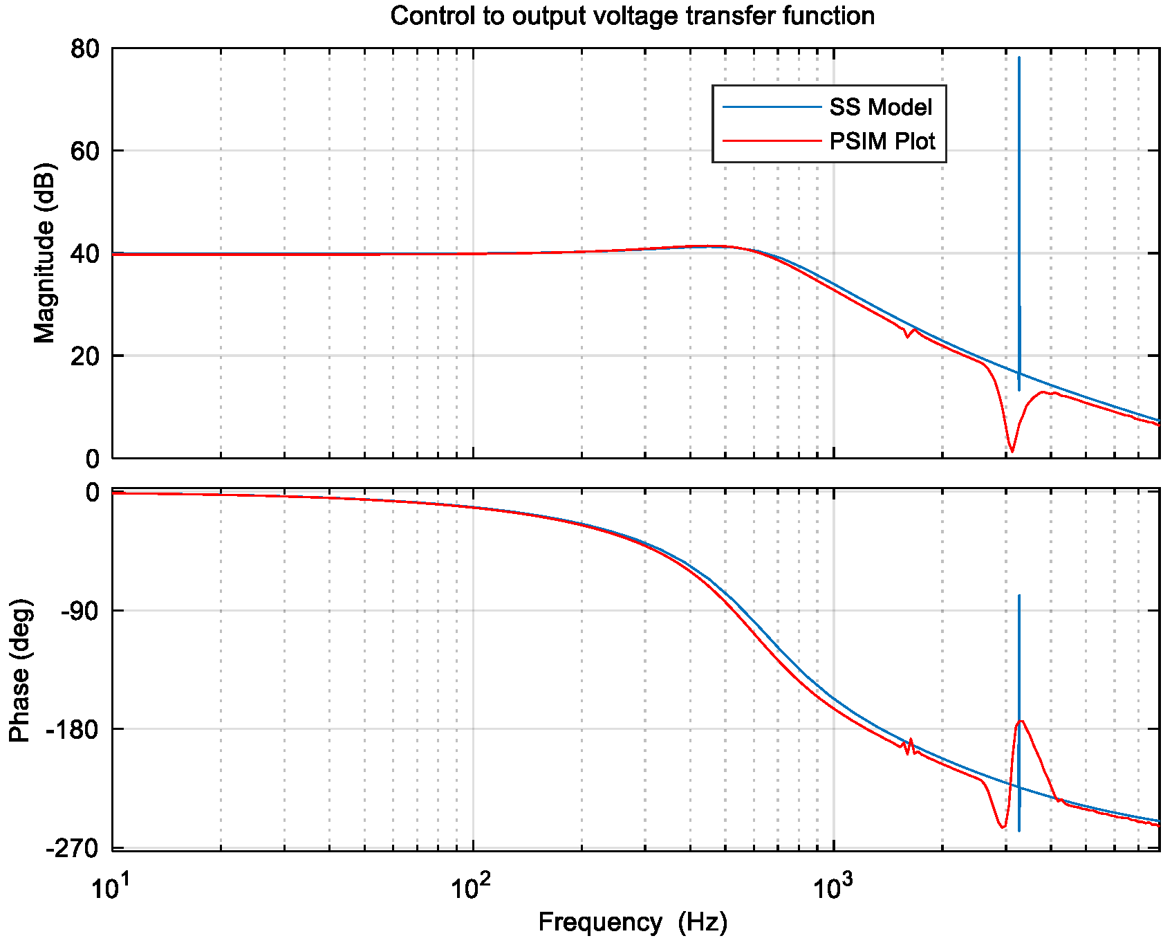
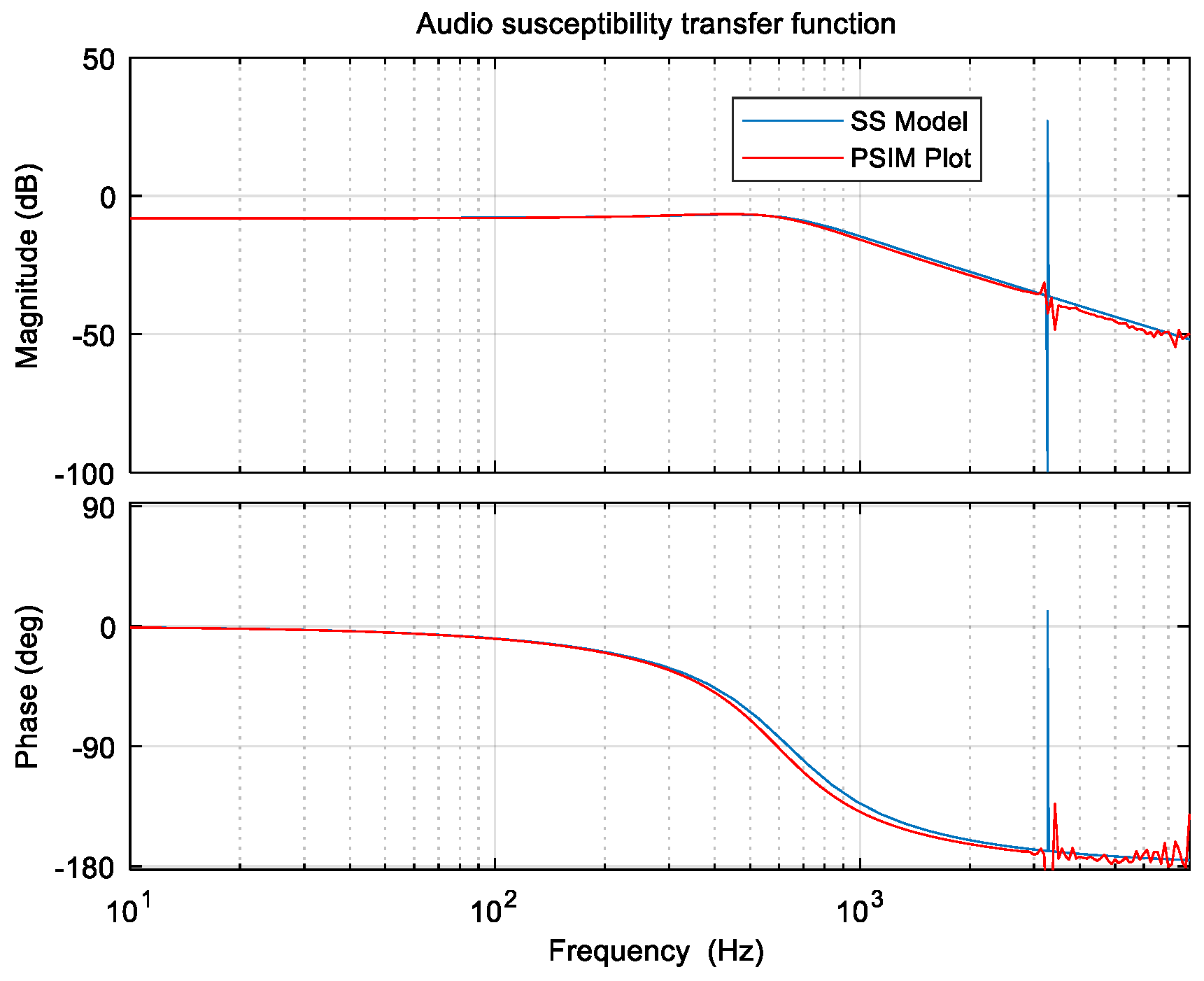
Similarly, the transfer functions shown in (42) and (43) were again used to draw an equivalent Bode plot to show the complete frequency response of the system. The corresponding numerical values for the components are shown in Table 7. In a similar manner, the same Bode plots were independently derived using the PSim AC sweep function with the same component values in Table 7. The PSim plots and model-based plots are shown on the same set of axes for control-to-output voltage transfer function (Figure 18) and audio-susceptibility (Figure 19).
v ˜ o s δ ˜ s v ˜ i n s = 0 = I L 1 + I L 2 C 1 L 1 L 2 s 3 + V C 1 C 1 L 1 + L 2 s 2 I L 1 L 1 s + V i n C 1 L 1 C 2 L 2 s 4 + C 1 L 1 L 2 R L s 3 + C 1 L 1 + L 2 1 D 2 + C 2 L 2 1 D 2 + D 2 C 2 L 1 s 2 + L 2 1 D 2 + D 2 L 1 R L s + 1 D 2
v ˜ o s v ˜ i n s δ ˜ s = 0 = 1 D C 1 L 2 s 2 + D 1 D C 1 L 1 C 2 L 2 s 4 + C 1 L 1 L 2 R L s 3 + C 1 L 1 + L 2 1 D 2 + C 2 L 2 1 D 2 + D 2 C 2 L 1 s 2 + L 2 1 D 2 + D 2 L 1 R L s + 1 D 2

5.4. Voltage-Fed Full-Bridge DC-DC Converter

5.4.1. Model Derivation

In Section 4.1 it was established that the voltage-fed full-bridge DC-DC converter in Figure 12 can be derived from an input-shunt, output-series connection of Type 1 BBBs. Additionally, it has been highlighted that g-parameters are more suited to model such a connection of BBBs. As such, the main task in modelling the complete circuit is to obtain equivalent g-parameter based two-port models for the identified BBBs and represent them as shown in (21) and (23). Once this is obtained, (26) and (27) can be directly evaluated to compute the control-to-output voltage transfer function and the audio-susceptibility transfer function, respectively.
From Figure 12, the structure of the BBB in red coincides with that of Type 1 with a diode connected to the rail. The two-port model of this BBB in terms of transmission parameters is readily available in Table 2, and also shown in (44). An equivalent model in terms of g-parameters is obtained based on (19). The results of (19) for the BBB in red are shown in (45).
[ v ˜ 1 ( s ) ι ˜ 1 ( s ) ] = [ 1 D s L 2 D 0 D ] [ v ˜ 2 ( s ) ι ˜ 2 ( s ) ] + [ V i n D I L ] δ ˜ ( s )
[ ι ˜ 1 ( u ) ( s ) v ˜ 2 ( u ) ( s ) ] = [ 0 D D s L 2 ] [ v ˜ 1 ( u ) ( s ) ι ˜ 2 ( u ) ( s ) ] + [ I L V i n ] δ ˜ ( s )
Similarly, the BBB in black coincides with that of Type 1 with a switch connected to the rail. It can be seen from Figure 12 that the input and output ports have been swapped for this BBB when compared to the model captured in Table 2. As such, inverse transmission parameters for this network must be computed to coincide with the power flow depicted in Figure 12. To do this, a conversion is made using (46). The computed inversion-transmission parameters in (47) can be considered as non-inverted transmission parameters for the power flow depicted in Figure 12. In a similar manner, the results of (47) can be converted using (19) to compute an equivalent g-parameter based model. The results of this conversion are shown in (48).
v ˜ 1 s ι ˜ 1 s = 1 det T D s B s C s A s v ˜ 2 s ι ˜ 2 s + 1 det T B s ι ˜ i n d T s D s v ˜ i n d T s A s ι ˜ i n d T s C s v ˜ i n d T s δ ˜ s
[ v ˜ 1 ( s ) ι ˜ 1 ( s ) ] = [ 1 1 D s L 2 ( 1 D ) 0 1 D ] [ v ˜ 2 ( s ) ι ˜ 2 ( s ) ] + [ V i n 1 D I L ] δ ˜ ( s )
[ ι ˜ 1 ( l ) ( s ) v ˜ 2 ( l ) ( s ) ] = [ 0 ( 1 D ) 1 D s L 2 ] [ v ˜ 1 ( l ) ( s ) ι ˜ 2 ( l ) ( s ) ] + [ I L V i n ] δ ˜ ( s )
To compute the final models, (45) and (48) are evaluated using (26) and (27) to obtain (49) and (50).
v ˜ o ( s ) δ ˜ ( s ) | v ˜ i n ( s ) = 0 = 2 V i n C L s 2 + L R L s + 1
v ˜ o ( s ) v ˜ i n ( s ) | δ ˜ ( s ) = 0 = 2 D 1 C L s 2 + L R L s + 1

5.4.2. Design Consideration and Comparisons

Similarly, the transfer functions shown in (49) and (50) were again used to draw an equivalent Bode plot to show the complete frequency response of the system. The corresponding numerical values for the components are shown in Table 8. In a similar manner, the same Bode plots were independently derived using the PSim AC sweep function with the same component values in Table 8. The PSim plots and model-based plots are shown on the same set of axes for control-to-output voltage transfer function (Figure 20) and audio-susceptibility (Figure 21).

6. Discussion

To validate models derived using the proposed modelling scheme, a baseline model needs to be established. Moreover, to assess the performance of the proposed modelling scheme, comparison must be made with competing modelling schemes.

6.1. Model Validation

The PSim AC sweep function is used to generate baseline models for any of the circuits considered in Section 5. The PSim models are generated directly from the switching circuit with an injecting circuitry in series with the perturbed signal. The amplitude of the injected signals are gradually increased with an increase in frequency. This is performed considering magnitude attenuation inherent in most practical systems at higher frequencies. The swept frequency range is limited to 40% of the switching frequency. The limitation in the frequency range considers the inherent limitation of averaged models, i.e., since switching action is ignored, averaged models are only accurate to about a third of the switching frequency [17,21]. Thus, a converter switching at 20 kHz will have an averaged model accurate to about 6.67 kHz. It should be noted that transfer functions derived using the proposed modelling scheme do not in any form have increased accuracy, i.e., any of the models derived here have the same accuracy as models derived in earlier studies, e.g., models in [17,20,21]. Thus, accuracy is still guaranteed up to a third of the switching frequency for models derived using the proposed scheme. However, there is decreased complexity and model computation time provided by the proposed scheme due to its inherent modularity and generalization of the power stage models.
The congruency of the Bode plots attained from the AC sweep function and those attained from analytical models derived using the proposed scheme is used to validate accuracy of the derived models. For any of the models evaluated in Section 5, it can be seen that the proposed modelling scheme accurately captures the dynamics of each converter considered in the study. The accuracy of the proposed modelling scheme is seen for both ideal and non-ideal models of the converters of interest. It can be seen from Table 5, (34), and (35) that Figure 14 and Figure 15 accurately represent non-ideal dynamics of the conventional buck-boost converter. Additionally, it can also be seen from Table 6, (38), and (39) that Figure 16 and Figure 17 accurately represent ideal dynamics of the conventional buck converter with an input filter.
It can be seen from Bode plots in Figure 18 and Figure 19 that the AC sweep does not capture sharp resonant points well. This is mainly attributed to the time step and the point-based signal injection operating mechanism of the AC sweep. Thus, an increase in the number of points will improve congruency of the analytical model with that of the AC sweep. In any case, the natural time constants of most practical converters will not permit such sharp resonant points. Thus, the congruency of the plots at resonant points should be evaluated considering practical implications of sharp points depicted in the Bode plots derived from analytical models.

6.2. Modelling Scheme Performance

The transmission parameter based two-port models in Table 2, Table 3 and Table 4 show that the proposed modelling scheme offers a seamless inclusion of non-ideal parameters for any of the converters considered in the study. This applies to both steady-state and dynamic models. This means non-monotonous gains due to non-ideal attributes will be accurately represented. Subsequently, controllers which are designed based on these models will perform with increased accuracy compared to models wherein non-ideal attributes are ignored. The use of BBBs to compute models refines the converter to its most basic form, thus providing more insight on converter make-up. Moreover, modelling the BBBs as two-port networks further simplifies the modelling procedure since the matrix size is curtailed to a 2 × 2 matrix throughout the modelling procedure. The generalization of the transfer functions of interest, as shown in (8)–(12), also simplifies the modelling procedure which would otherwise be accompanied by tedious algebra. Ultimately, the use of the proposed modelling scheme nullifies converter order and functionality in the modelling procedure which further simplifies the process.
To model BBBs, generic modelling schemes are employed; as such, most of the merits of the proposed scheme exist, provided that the information contained in Table 2, Table 3 and Table 4 is at one’s disposal. It should be noted that the circuit averaging modelling technique was employed to come up with equivalent linear circuit models (Figure 5, Figure 6, Figure 8 and Figure 9) of the BBBs, from which two-port models were derived.
Although the computation of alternative two-port parameters of a two-port network are standardized, computing alternative parameters may present a computational burden. However, generalization of transfer functions for alternative parameters, as shown in (26), (27), (30), and (31), counters this burden since it reduces computational effort. It should be noted that (19) can be substituted into (26) and (27) to directly compute models of interest, which can further reduce computational effort. A similar substitution can be performed on (30) and (31).

6.3. Modelling Scheme Highlights

When comparing the proposed modelling scheme to more closely related modelling schemes, such as the layer or graft scheme, the proposed method seems to retain the converter family classification of the buck-boost converter described in [28]. On the other hand, the other schemes consider the buck-boost converter as a byproduct of the layer or graft scheme. Thus, based on the proposed scheme, the buck-boost converter can still be considered a result of the permutation of the Type 1 BBB, or equivalently, converter cell A [28]. The use of lumped Type 2 BBBs shows close ties among the Cuk converter, Sepic converter, and the Zeta converter. According to the classification in [28], only the Sepic and Zeta converters belong to the same group.
Using the proposed modelling scheme, non-conventional converters can be modelled solely based on identified BBBs and corresponding circuit connection. Thus, there is no need to know more about circuit behavior. The only prior knowledge one would need to model a converter rests entirely on identifying the predefined BBBs and how they are connected in the circuit. This fact is validated with an example based on modelling a voltage-fed full-bridge DC-DC converter in Figure 11. It was shown in Section 5.4 that the models given by (49) and (50) were computed solely based on BBB models and their connection in the circuit of interest. This attribute makes the proposed scheme modular and will prove important when modelling new converters containing the specified BBBs.

7. Conclusions

In this paper, the use of BBBs to compute small-signal and steady-state models of commonly used converters is evaluated. It was found that only Type 1, Type 2, and the filter block are sufficient to model all the converters of interest. A modelling scheme based on modelling BBBs as two-port networks and computing equivalent models in a circuit synthesis-oriented manner was proposed. The proposed modeling scheme was shown to add modularity in the modelling procedure which makes it more suited for modelling large interconnected systems such as converters in a DC microgrid. Additionally, the proposed modelling scheme enabled the models of interest to be generalized based on two-port network attributes. Converter order and functionality were shown to be immaterial in computing models of interest for any of the converters considered in the study. Furthermore, non-ideal parameters which capture practical component limitations were shown to be captured with ease in the proposed scheme. The proposed modelling scheme was shown to seamlessly model non-conventional converters whose circuits can be refined into identified BBBs. The accuracy of the models computed using the proposed modelling scheme was validated using Bode plots computed using the PSim AC sweep function. The resultant plots drawn from the derived models and those derived from the AC sweep were shown to be congruent when drawn on the same set of axes. The proposed modelling scheme is anticipated to simplify the modelling of current and new converters deployed in DC microgrids, provided that such converters can be refined into identified BBBs.

Author Contributions

Conceptualization, L.M.; methodology, L.M.; software, L.M.; validation, L.M. and M.N.G.; formal analysis, L.M.; investigation, L.M. and M.N.G.; data curation, M.N.G.; writing—original draft preparation, L.M.; writing—review and editing, L.M. and M.N.G.; visualization, L.M. and M.N.G.; supervision, M.N.G.; project administration, L.M. and M.N.G. All authors have read and agreed to the published version of the manuscript.

Funding

This research received no external funding.

Data Availability Statement

All generated data is contained in the manuscript.

Acknowledgments

The authors would like to thank the national research foundation (NRF) for their support during the course of the research.

Conflicts of Interest

The authors declare no conflict of interest. The funders had no role in the design of the study; in the collection, analyses, or interpretation of data; in the writing of the manuscript, or in the decision to publish the results.

References

  1. Mohan, N.; Undeland, T.M.; Robbins, W.P. Power Electronics: Converters, Applications and Design, 2nd ed.; Wiley: New York, NY, USA, 1995. [Google Scholar]
  2. Sreekumar, A.; Jiji, K.S. A Survey of DC-DC Converters for Fuel Cell Electric Vehicle Applications. In Proceedings of the 2021 2nd International Conference for Emerging Technology (INCET), Belagavi, India, 21–23 May; 2021; pp. 1–5. [Google Scholar]
  3. Li, B.; Liu, J.; Wang, Z.; Zhang, S.; Xu, D. Modular High-Power DC–DC Converter for MVDC Renewable Energy Collection Systems. IEEE Trans. Ind. Electron. 2021, 68, 5875–5886. [Google Scholar] [CrossRef]
  4. Li, L.; Li, B.; Wang, Z.; Yang, M.; Xu, D. Monopolar Symmetrical DC–DC Converter for All DC Offshore Wind Farms. IEEE Trans. Power Electron. 2022, 37, 4275–4287. [Google Scholar] [CrossRef]
  5. Tonolo, É.A.; Soares, J.W.M.; Romaneli, E.F.R.; Badin, A.A. Current Sensorless MPPT with a CCM Interleaved Boost Converter for Renewable Energy System. IEEE Trans. Power Electron. 2022, 37, 11296–11304. [Google Scholar] [CrossRef]
  6. Verma, D.; Nema, S.; Agrawal, R.; Sawle, Y.; Kumar, A. A Different Approach for Maximum Power Point Tracking (MPPT) Using Impedance Matching through Non-Isolated DC-DC Converters in Solar Photovoltaic Systems. Electronics 2022, 11, 1053. [Google Scholar] [CrossRef]
  7. Sousa, S.M.; Gusman, L.S.; Lopes, T.A.S.; Pereira, H.A.; Callegari, J.M.S. MPPT algorithm in single loop current-mode control applied to dc–dc converters with input current source characteristics. Int. J. Electr. Power Energy Syst. 2022, 138, 107909. [Google Scholar] [CrossRef]
  8. Pandey, R.; Singh, B. A Cuk Converter and Resonant LLC Converter Based E-Bike Charger for Wide Output Voltage Variations. IEEE Trans. Ind. Appl. 2021, 57, 2682–2691. [Google Scholar] [CrossRef]
  9. Rathore, V.; Siddavatam, R.P.R.; Rajashekara, K. An Isolated Multilevel DC-DC Converter Topology with Hybrid Resonant Switching for EV Fast Charging Application. IEEE Trans. Ind. Appl. 2022, 58, 5546–5557. [Google Scholar] [CrossRef]
  10. Hossain MR, T.; Abedin, A.H.; Choudhury, M.A. A single phase SEPIC AC-DC Converter with improved power factor and input current THD. In Proceedings of the 2016 9th International Conference on Electrical and Computer Engineering (ICECE), Bhaka, Bangladesh, 20–22 December; pp. 373–376.
  11. Premkumar, K.; Vishnupriya, M.; Thamizhselvan, T.; Sanjeevikumar, P.; Manikandan, B. PSO optimized PI controlled DC-DC buck converter-based proton-exchange membrane fuel cell emulator for testing of MPPT algorithm and battery charger controller. Int. Trans. Electr. Energy Syst. 2020, 31, e12754. [Google Scholar] [CrossRef]
  12. De Beer, C.; Barendse, P.; Khan, A. Development of an HT PEM Fuel Cell Emulator Using a Multiphase Interleaved DC–DC Converter Topology. IEEE Trans. Power Electron. 2013, 28, 1120–1131. [Google Scholar] [CrossRef]
  13. Wang, D.; Chen, H.; Huang, Y.; Deng, X.; Zhu, G. Modeling and Stability Analysis of Weak-Grid Tied Multi-DFIGs in DC-Link Voltage Control Timescale. Energies 2020, 13, 3689. [Google Scholar] [CrossRef]
  14. Tseng, K.; Cheng, C.; Chen, C. High step-up boost converter for distributed generation using renewable and alternative power sources. IEEE J. Emerg. Sel. Top. Power Electron. 2017, 5, 713–722. [Google Scholar] [CrossRef]
  15. Das, M.; Agarwal, V. Generalized Small Signal Modeling of Coupled-Inductor-Based High-Gain High-Efficiency DC–DC Converters. IEEE Trans. Ind. Appl. 2017, 53, 2257–2270. [Google Scholar] [CrossRef]
  16. Muchina, E.G.; Masike, L.; Gitau, M.N. High Boost-Ratio Bidirectional converter for interfacing low-voltage battery energy storage systems to a dc bus. IET Power Electron. 2019, 12, 2372–2381. [Google Scholar] [CrossRef]
  17. Masike, L.; Gitau, M.N.; Adam, G.P. A Unified Rule-Based Small-Signal Modelling Technique for Two-Switch, Non-Isolated DC–DC Converters in CCM. Energies 2022, 15, 5454. [Google Scholar] [CrossRef]
  18. Cuk, S. Modelling, Analysis and Design of Switching Converters. Ph.D. Thesis, California Institute of Technology, Pasedena, CA, USA, November 1976. [Google Scholar]
  19. Wester, G.W. Low-Frequency Characterization of Switched DC-DC Converters. Ph.D. Thesis, California Institute of Technology, Pasedena, CA, USA, May 1972. [Google Scholar]
  20. Middlebrook, R.D.; Cuk, S. A general unified approach to modelling switching-converter power stages. In Proceedings of the IEEE Power Electronics Specialists Conference, Cleveland, OH, USA, 8–10 June 1976; pp. 18–34. [Google Scholar]
  21. Wester, G.W.; Middlebrook, R.D. Low-Frequency Characterization of Switched dc-dc Converters. IEEE Trans. Aerosp. Electron. Syst. 1973, AES-9, 376–385. [Google Scholar] [CrossRef] [Green Version]
  22. Smedley, K.; Cuk, S. Switching Flow-Graph nonlinear modeling technique. IEEE Trans. Power Electron. 1994, 9, 405–413. [Google Scholar] [CrossRef] [Green Version]
  23. Luo, F.L.; Ye, H. Small Signal Analysis of Energy Factor and Mathematical Modeling for Power DC–DC Converters. IEEE Trans. Power Electron. 2007, 22, 69–79. [Google Scholar] [CrossRef]
  24. Kumar, R.; Pathak, M.K. Control of DC Microgrid for Improved Current Sharing and Voltage Regulation. In Proceedings of the 2020 3rd International Conference on Energy, Power and Environment: Towards Clean Energy Technologies, Shilong, India, 5–7 March 2021; pp. 1–4. [Google Scholar]
  25. Karami, Z.; Shafiee, Q.; Sahoo, S.; Yaribeygi, M.; Bevrani, H.; Dragicevic, T. Hybrid Model Predictive Control of DC–DC Boost Converters with Constant Power Load. IEEE Trans. Energy Convers. 2021, 36, 1347–1356. [Google Scholar] [CrossRef]
  26. Soriano-Rangel, C.A.; He, W.; Mancilla-David, F.; Ortega, R. Voltage Regulation in Buck–Boost Converters Feeding an Unknown Constant Power Load: An Adaptive Passivity-Based Control. IEEE Trans. Control Syst. Technol. 2021, 29, 395–402. [Google Scholar] [CrossRef]
  27. Punna, S.; Mailugundla, R.; Salkuti, S.R. Design, Analysis and Implementation of Bidirectional DC–DC Converters for HESS in DC Microgrid Applications. Smart Cities 2022, 5, 433–454. [Google Scholar] [CrossRef]
  28. Tymerski, R.; Vorperian, V. Generation, classification and analysis of switch-mode DC-DC converters by the use of converter cells. In Proceedings of the Telecommunications Energy Conference, Toronto, ON, Canada, 19–22 October 1986; pp. 181–195. [Google Scholar]
  29. Williams, B.W. Generation and analysis of canonical switching cell DC-DC converters. IEEE Trans. Ind. Electron. 2014, 61, 329–346. [Google Scholar] [CrossRef]
  30. Landsman, E.E. A unifying derivation of switching regulator topologies. In Proceedings of the IEEE PESC Record, San Diego, CA, USA, 18–22 June 1979; pp. 239–243. [Google Scholar]
  31. Williams, B.W. DC-DC converters with continuous input and output power. IEEE Trans. Power Electron. 2013, 28, 2307–2316. [Google Scholar] [CrossRef]
  32. Erickson, R.W. Synthesis of switch-mode converters. In Proceedings of the IEEE PESC Record, Albuquerque, NM, USA, 6–9 June 1983; pp. 9–22. [Google Scholar]
  33. Gitau, M.N.; Adams, G.P.; Masike, L.; Mbukani, M.K. Unified approach to synthesis and analysis of non-isolated DC-DC converters. IEEE Access 2021, 9, 120088–120109. [Google Scholar] [CrossRef]
  34. Khateb, A.H.; Rahim, N.; Selvaraj, J.; Williams, B.W. DC-DC converter with low input current ripple for maximum photovoltaic power extraction. IEEE Trans. Ind. Electron. 2015, 62, 2246–2256. [Google Scholar]
  35. Lee, Y.S. A Systematic and Unified Approach to Modeling Switches in Switch-Mode Power Supplies. IEEE Trans. Ind. Electron. 1985, IE-32, 445–448. [Google Scholar] [CrossRef]
  36. Vorperian, V. Simplified analysis of PWM converters using model of PWM switch. Continuous conduction mode. IEEE Trans. Aerosp. Electron. Syst. 1990, 26, 490–496. [Google Scholar] [CrossRef]
  37. Tymerski, R.; Vorperian, V.; Lee FC, Y.; Baumann, W.T. Nonlinear modeling of the PWM switch. IEEE Trans. Power Electron. 1989, 4, 225–233. [Google Scholar] [CrossRef]
  38. Wu, T.F.; Chen, Y.K. A systematic and unified approach to modeling PWM DC/DC converters using the layer scheme. In Proceedings of the PESC Record. 27th Annual IEEE Power Electronics Specialists Conference, Baveno, Italy, 23–27 June 1996; pp. 575–580. [Google Scholar]
  39. Wu, T.F.; Chen, Y.K. A systematic and unified approach to modeling PWM DC/DC converters based on the graft scheme. IEEE Trans. Ind. Electron. 1998, 45, 88–98. [Google Scholar]
  40. Yao, J.; Li, K.; Zheng, K.; Abramovitz, A. A unified modeling approach to Tapped Inductor Converters Accounting for the Leakage Inductance Effects. IEEE Trans. Power Electron. 2022, 37, 13047–13059. [Google Scholar] [CrossRef]
  41. Abramovitz, A.; Yao, J.; Smedley, K. Unified Modeling of PWM Converters with Regular or Tapped Inductors Using TIS-SFG Approach. IEEE Trans. Power Electron. 2016, 31, 1702–1716. [Google Scholar] [CrossRef]
  42. Walker, G.R.; Sernia, P.C. Cascaded DC-DC converter connection of photovoltaic modules. IEEE Trans. Power Electron. 2004, 19, 1130–1139. [Google Scholar] [CrossRef]
  43. EIsmail, H.; Al-Saffar, M.A.; Sabzali, A.J.; Fardoun, A.A. High voltage gain single-switch non-isolated DC-DC converters for renewable energy applications. In Proceedings of the IEEE International Conference on Sustainable Energy Technologies (ICSET), Kandy, Sri Lanka, 6–9 December 2010; pp. 1–6. [Google Scholar]
  44. Shahir, F.M.; Babaei, E.; Aberoumandazar, M. New single-switch non-isolated boost DC-DC converter with free input current ripple. In Proceedings of the IEEE PEDSTC Conference, Tabriz, Iran, 2–4 February 2021. [Google Scholar]
  45. Sarvghadi, P.; Varjani AYand Shahparasti, M. A High Step-up Transformerless DC–DC Converter with New Voltage Multiplier Cell Topology and Coupled Inductor. IEEE Trans. Ind. Electron. 2022, 69, 10162–10171. [Google Scholar] [CrossRef]
  46. Veerachary, M. Analysis of Fourth-Order DC-DC Converters: A Flow Graph Approach. IEEE Trans. Ind. Electron. 2008, 55, 133–141. [Google Scholar] [CrossRef]
  47. Alexander, C.K.; Sadiku MN, O. Fundamentals of Electric Circuits, 5th ed.; McGraw-Hill: New York, NY, USA, 2013. [Google Scholar]
  48. Erickson, R.W.; Maksimovic, D. Fundamentals of Power Electronics, 2nd ed.; Kluwer Academic Publishers: New York, NY, USA, 2001. [Google Scholar]
Figure 1. BBBs proposed in [33]. (a) a Type 1 BBB, (b) variant 1 of a Type 2 BBB, (c) Vvariant 2 of a Type 2 BBB, (d) a Type 3 BBB, and (e) the filter block.
Energies 16 01047 g001
Figure 2. Example converters. (a) a buck converter with input filter, and (b) a Cuk converter.
Energies 16 01047 g002
Figure 3. Generalised circuit diagram.
Energies 16 01047 g003
Figure 4. Rail connection variants for a Type 1 BBB. (a) Switch to rail, (b) diode to rail, and (c) inductor to rail.
Energies 16 01047 g004
Figure 5. Ideal averaged small-signal/steady-state equivalent circuit for Type 1 BBB variants. (a) Switch to rail, (b) diode to rail, and (c) inductor to rail.
Energies 16 01047 g005
Figure 6. Non-ideal averaged small-signal/steady-state equivalent circuit for Type 1 BBB variants. (a) Switch to rail, (b) diode to rail, and (c) inductor to rail.
Energies 16 01047 g006
Figure 7. Rail connection variants for the lumped Type 2 BBBs. (a) Switch and diode to rail, (b) Inductor and switch to rail, and (c) inductor and diode to rail.
Energies 16 01047 g007
Figure 8. Rail connection variants for the ideal lumped Type 2 BBBs. (a) Switch and diode to rail, (b) inductor and switch to rail, and (c) inductor and diode to rail.
Energies 16 01047 g008
Figure 9. Rail connection variants for the non-ideal lumped Type 2 BBBs. (a) Switch and diode to rail, (b) inductor and switch to rail, and (c) inductor and diode to rail.
Energies 16 01047 g009
Figure 10. Filter block circuit diagrams. (a) Filter components, (b) ideal filter components, and (c) non−ideal filter components.
Energies 16 01047 g010
Figure 11. Voltage-fed DC-DC converter.
Energies 16 01047 g011
Figure 12. Refined circuitry of a voltage-fed DC-DC converter.
Energies 16 01047 g012
Figure 13. Current-fed full-bridge DC-DC converter.
Energies 16 01047 g013
Figure 14. Control−to−output voltage transfer function for a buck−boost converter.
Energies 16 01047 g014
Figure 15. Audio−susceptibility transfer function for a buck−boost converter.
Energies 16 01047 g015
Figure 16. Control−to−output voltage transfer function for a buck converter with an input filter.
Energies 16 01047 g016
Figure 17. Audio−susceptibility transfer function for a buck converter with an input filter.
Energies 16 01047 g017
Figure 18. Control-to-output voltage transfer function for the Sepic converter.
Energies 16 01047 g018
Figure 19. Audio−susceptibility transfer function for the Sepic converter.
Energies 16 01047 g019
Figure 20. Control−to−output voltage transfer function for a Voltage−fed full bridge converter.
Energies 16 01047 g020
Figure 21. Audio−susceptibility transfer function for a Voltage−fed full bridge converter.
Energies 16 01047 g021
Table 1. Converters considered in the study.
ConverterMerits
BuckLow component count
BoostLow component count
Buck-boostLow component count
CukLow component count, buck-boost functionality, continuous input and output current
Boost with output filterContinuous input and output current, low component count
Buck with input filterContinuous input and output current, low component count
Buck with output filterLow component count
Boost with input filterLow component count
Buck-boost with input filterContinuous input current, low component count
Buck-boost with output filterContinuous output current, low component count
SepicNon-inverting buck-boost function, continuous input current, low component count
ZetaNon-inverting buck-boost function, continuous input current, low component count
Table 2. Small-signal and steady-state models for Type 1 BBB.
BBB VariantModel StateIdealNon-Ideal
Type 1: Switch to railSmall-signal (1a) [ v ˜ 1 ( s ) ι ˜ 1 ( s ) ] = [ 1 D s L 1 1     D 0 1 1     D ] [ v ˜ 2 ( s ) ι ˜ 2 ( s ) ] + [ V i n     s L 1 I L 1     D I L 1     D ] δ ˜ ( s ) [ v ˜ 1 ( s ) ι ˜ 1 ( s ) ] = [ 1 D R o n D + Z L ( 1     D ) 0 1 1     D ] [ v ˜ 2 ( s ) ι ˜ 2 ( s ) ] + [ I L [ R o n   +   Z L ] [ 1     D ] [ V o   +   V f w d ] 1     D I L 1     D ] δ ˜ ( s )
Steady-State (1b) [ V 1 I 1 ] = [ 1 D 0 0 1 1     D ] [ V 2 I 2 ] + [ 0 0 ] [ V 1 I 1 ] = [ 1 D R o n D   +   r L ( 1     D ) 0 1 1 D ] [ V 2 I 2 ] + [ ( 1     D ) V f w d 0 ]
Type 1: Diode to railSmall-signal (1a) [ v ˜ 1 ( s ) ι ˜ 1 ( s ) ] = [ 1 D s L 1 D 0 D ] [ v ˜ 2 ( s ) ι ˜ 2 ( s ) ] + [ V i n D I L ] δ ˜ ( s ) [ v ˜ 1 ( s ) ι ˜ 1 ( s ) ] = [ 1 D R o n D   +   Z L D 0 D ] [ v ˜ 2 ( s ) ι ˜ 2 ( s ) ] + [ [ R o n I L     ( V i n   +   V f w d ) ] D I L ] δ ˜ ( s )
Steady-State (1b) [ V 1 I 1 ] = [ 1 D 0 0 D ] [ V 2 I 2 ] + [ 0 0 ] [ V 1 I 1 ] = [ 1 D + R o n D   +   r L D 0 D ] [ V 2 I 2 ] + [ ( 1     D ) V f w d D 0 ]
Type 1: Inductor to railSmall-signal (1a) [ v ˜ 1 ( s ) ι ˜ 1 ( s ) ] = [ ( 1     D ) D s L 1 D ( 1     D ) 0 D 1     D ] [ v ˜ 2 ( s ) ι ˜ 2 ( s ) ] + [ V i n     s L 1 I L D ( 1     D ) I L ( 1     D ) ] δ ˜ ( s ) [ v ˜ 1 ( s ) ι ˜ 1 ( s ) ] = [ ( 1     D ) D R o n D   +   Z L D ( 1     D ) 0 D 1     D ] [ v ˜ 2 ( s ) ι ˜ 2 ( s ) ] + [ ( R o n   +   Z L ) I L     ( V i n     V o   +   V f w d ) ( 1     D ) D ( 1     D ) I L 1     D ] δ ˜ ( s )
Steady-State (1b) [ V 1 I 1 ] = [ ( 1     D ) D 0 0 D 1     D ] [ V 2 I 2 ] + [ 0 0 ] [ V 1 I 1 ] = [ ( 1     D ) D R o n D   +   r L D ( 1     D ) 0 D 1     D ] [ V 2 I 2 ] + [ ( 1     D ) V f w d D 0 ]
Table 3. Small-signal and steady-state models for the lumped Type 2 BBBs.
BBB VariantModel StateIdealNon-Ideal
Lumped Type 2 BBBs: Switch and diode to railSmall-signal (1a) v ˜ 1 s ι ˜ 1 s = C 1 L 1 s 2 + 1 D 2 D 1 D s L 1 D 1 D s C 1 D 1 D D 1 D v ˜ 2 s ι ˜ 2 s + D I b s L 1 V a C 1 L 1 s 2 + 1 D D 1 D 2 D I b s C 1 V a D 1 D 2 δ ˜ s v ˜ 1 s ι ˜ 1 s = Z L 1 + 1 D 2 Z C 1 + D R o n D 1 D Z C 1 D R o n Z L 1 R o n + Z C 1 D + R o n Z C 1 R o n 1 D Z C 1 1 D 1 D Z C 1 D R o n R o n + Z C 1 D R o n 1 D Z C 1 v ˜ 2 s ι ˜ 2 s + I b D Z C 1 Z L 1 + R o n Z C 1 + Z L 1 V a + V b + V f w d 1 D Z C 1 1 D + Z L 1 D 1 D 1 D Z C 1 R o n I b D Z C 1 + R o n V a + V b + V f w d 1 D D 1 D 1 D Z C 1 R o n δ ˜ s
Steady-State (1b) [ V 1 I 1 ] = [ ( 1 D ) D 0 0 D ( 1 D ) ] [ V 2 I 2 ] + [ 0 0 ] [ V 1 I 1 ] = [ ( 1 D ) D ( D r L 1 + R o n ) ( 1 D ) 0 D ( 1 D ) ] [ V 2 I 2 ] + [ ( 1 D ) D V f w d 0 ]
Lumped Type 2 BBBs: inductor and switch to railSmall-signal (1a) v ˜ 1 s ι ˜ 1 s = C 1 L 1 s 2 + 1 1 D C 1 L 1 s 2 + D s L 1 1 D C 1 L 1 s 2 + D s C 1 1 D C 1 L 1 s 2 + D C 1 L 1 s 2 + D 2 1 D C 1 L 1 s 2 + D v ˜ 2 s ι ˜ 2 s + V i n C 1 L 1 s 2 + 1 1 D C 1 L 1 s 2 + D I b C 1 L 1 s 2 + D V i n C s 1 D 2 1 D 2 C 1 L 1 s 2 + D δ ˜ s v ˜ 1 s ι ˜ 1 s = Z C 1 + Z L 1 1 D Z C 1 D + Z L 1 D R o n Z C 1 + Z L 1 + Z L 1 Z C 1 1 D 2 1 D Z C 1 D + Z L 1 1 D Z C 1 D + Z L 1 D R o n + Z L 1 + Z C 1 D 2 1 D Z C 1 D + Z L 1 v ˜ 2 s ι ˜ 2 s + I b R o n Z C 1 D + Z L 1 V a + V b + V f w d 1 D 2 Z C 1 D + Z L 1 + Z L 1 1 D 3 D 1 D 2 D Z C 1 + Z L 1 I b D Z C 1 D + Z L 1 Z C 1 + Z L 1 + V a + V b + V f w d 1 D 2 Z C 1 D + Z L 1 Z L 1 1 D 3 D 1 D 2 D Z C 1 + Z L 1 Z C 1 + Z L 1 δ ˜ s
Steady-State (1b)   [ V 1 I 1 ] = [ ( 1 D ) D 0 0 D ( 1 D ) ] [ V 2 I 2 ] + [ 0 0 ] [ V 1 I 1 ] = [ ( 1 D ) D D R o n + ( 1 D ) 2 r L 1 D ( 1 D ) 0 D ( 1 D ) ] [ V 2 I 2 ] + [ ( 1 D ) D V f w d 0 ]
Lumped Type 2 BBBs: Inductor and diode to railSmall-signal (1a) v ˜ 1 s ι ˜ 1 s = C 1 L 1 s 2 + 1 D 2 D C 1 L 1 s 2 + 1 D s L 1 D C 1 L 1 s 2 + 1 D s C 1 D C 1 L 1 s 2 + 1 D C 1 L 1 s 2 + 1 D C 1 L 1 s 2 + 1 D v ˜ 2 s ι ˜ 2 s + I o D s L 1 V i n C 1 L 1 s 2 + 1 D D 1 D C 1 L 1 s 2 + 1 D I o C 1 L 1 s 2 + 1 1 D C 1 L 1 s 2 + 1 D δ ˜ s v ˜ 1 s ι ˜ 1 s = D R o n + Z L 1 + Z C 1 1 D 2 D Z C 1 1 D + Z L 1 D R o n Z C 1 + Z L 1 + Z L 1 Z C 1 D 2 D Z C 1 1 D + Z L 1 D Z C 1 1 D + Z L 1 Z C 1 + Z L 1 D Z C 1 1 D + Z L 1 v ˜ 2 s ι ˜ 2 s + R o n Z C 1 + Z L 1 + D Z C 1 Z L 1 I b V a + V b + V f w d 1 D Z C 1 1 D + Z L 1 1 D Z C 1 1 D + Z L 1 Z C 1 + Z L 1 I b 1 D Z C 1 1 D + Z L 1 δ ˜ s
Steady-State (1b) [ V 1 I 1 ] = [ ( 1 D ) D 0 0 D ( 1 D ) ] [ V 2 I 2 ] + [ 0 0 ] [ V 1 I 1 ] = [ ( 1 D ) D R o n + D r L 1 ( 1 D ) 0 D ( 1 D ) ] [ V 2 I 2 ] + [ ( 1 D ) D V f w d 0 ]
Table 4. Small-signal and steady-state models for the filter block.
BBB VariantModel StateIdealNon-Ideal
Generalised LCL filter blockSmall-signal (1a) [ v ˜ 1 ( s ) ι ˜ 1 ( s ) ] = [ C 1 L 1 s 2 + 1 C 1 L 1 L 2 s 3 + s ( L 1 + L 2 ) s C 1 C 1 L 2 s 2 + 1 ] [ v ˜ 2 ( s ) ι ˜ 2 ( s ) ] [ v ˜ 1 ( s ) ι ˜ 1 ( s ) ] = [ Z L 1 Z C 1 + 1 Z L 1 ( Z L 2 + Z C 1 ) + Z L 2 Z C 1 Z C 1 1 Z C 1 Z L 2 Z C 1 + 1 ] [ v ˜ 2 ( s ) ι ˜ 2 ( s ) ] Z L 1 = s L 1 + r L 1 ;   Z L 2 = s L 2 + r L 2 ;   Z C 1 = 1 + r C 1 C 1 s C 1 s
Steady-state (1b) [ V 1 I 1 ] = [ 1 0 0 1 ] [ V 2 I 2 ] + [ 0 0 ] [ V 1 I 1 ] = [ 1 r L 1 + r L 2 0 1 ] [ V 2 I 2 ] + [ 0 0 ]
Table 5. Buck-boost converter parameters.
ComponentValue
V o 20 V
V i n 50 V
P o 200 W
F s w 20 kHz
R o n ; V f w d 40 mΩ; 1.1 V
r L ;   r C 30 mΩ; 3 mΩ
i L , p k p k ;   v o , p k p k 0.2 I L ;     0.02 V o
D 0.305
L ; C 259.64 µH; 381.25 µF
Table 6. Buck converter with input filter parameters.
ComponentValue
V o 50 V
V i n 100 V
P o 250 W
F s w 50 kHz
R o n ; V f w d 0 Ω; 0 V
r L 1 = r L 2 = r C 1 = r C 1 0 Ω
i L , p k p k ;   v o , p k p k 0.2 I L ;     0.02 V o
D 0.4
L 1 ;   L 2 ; C 1 ;   C 2 500 µH; 300 µH; 20 µF; 31.25 µF
Table 7. Sepic converter parameteres.
ComponentValue
V o 20 V
V i n 50 V
P o 200 W
F s w 20 kHz
R o n ; V f w d 0 Ω; 0 V
r L 1 = r L 2 = r C 1 = r C 1 0 Ω
i L 2 , p k p k ;   v o , p k p k 0.2 I L 2 ;     0.02 V o
D 0.2857
L 1 ;   L 2 ; C 1 ;   C 2 357.1428 µH; 357.1428 µH; 57.1428 µF; 142.857 µF
Table 8. Voltage-fed full-bridge converter parameters.
ComponentValue
V o 20 V
V i n 50 V
P o 200 W
F s w 20 kHz
R o n ; V f w d 0 Ω; 0 V
r L = r C 0 Ω
i L , p k p k ;   v o , p k p k 0.2 I L ;     0.02 V o
D 0.7
L ;   C 525 µH; 31.25 µF
Disclaimer/Publisher’s Note: The statements, opinions and data contained in all publications are solely those of the individual author(s) and contributor(s) and not of MDPI and/or the editor(s). MDPI and/or the editor(s) disclaim responsibility for any injury to people or property resulting from any ideas, methods, instructions or products referred to in the content.