Article

Detailed Controller Synthesis and Laboratory Verification of a Matching-Controlled Grid-Forming Inverter for Microgrid Applications

by
Edgar Diego Gomez Anccas
*,†,
Kazem Pourhossein
,
Daniel Becker
and
Detlef Schulz
Electrical Power Systems, Faculty of Electrical Engineering, Helmut Schmidt University/University of the Federal Armed Forces Hamburg, 22043 Hamburg, Germany
*
Author to whom correspondence should be addressed.
These authors contributed equally to this work.
Energies 2023, 16(24), 8079; https://doi.org/10.3390/en16248079
Submission received: 14 October 2023 / Revised: 5 December 2023 / Accepted: 7 December 2023 / Published: 15 December 2023
(This article belongs to the Special Issue Grid-Forming Technologies for Renewable Energy Integration)

Abstract

:
Grid-forming inverters are the essential components in the effort to integrate renewable energy resources into stand-alone power systems and microgrids. Performance of these inverters directly depends on their control parameters embodied in the controller. Even the most conscientiously designed controller will exhibit suboptimal performance upon implementation due to the presence of parasitic elements in the existing hardware. Hence, the controller has to be tuned and optimized. In the present article, the process of implementation, laboratory verification, and tuning of a matching-controlled grid-forming inverter is presented. In order to assess the efficiency of the grid-forming controller, its operation has been tested and analyzed in blackstart, steady state, and transient operation. For this purpose, a systematic sensitivity analysis has been conducted and the control parameters have been tuned in laboratory tests. The laboratory results verify proper operation of a 7 kW grid-forming inverter in all three test scenarios. After applying the proposed method on the tested grid-forming inverter in steady state operation, total harmonic distortion (THD) of the output voltage is less than 0.5% for its practical loading range (maximum THD is less than 1% in no-load condition). The system is able to blackstart and supply the loads. Finally, the studied grid-forming inverter is stable in the presence of severe step load changes and disturbances, i.e., voltage overshoot is managed well and compensated for with a low settling time using this approach.

1. Introduction

In recent decades, by integrating renewable energy resources and energy storage devices into the electric power grid, microgrids, or other electrical energy systems, power electronics have played and continue to play an increasingly crucial role to convert electrical power and control energy flow in electric energy supply [1]. In this regard, grid-tied inverters are key components. These inverters can be roughly divided into two categories: grid-following inverters (GFLIs) and grid-forming inverters (GFMIs) [1,2].
A GFLI can be considered as a controlled current source in the presence of a parallel high impedance that can control the injected current as well as supply power to the grid or regulate the output voltage.
Conversely, a GFMI can be considered a controlled voltage source in series with a low impedance. GFMIs control the output power by directly controlling their output voltage and are thus able to provide a reference voltage for GFLI and other equipment in the grid such as electrical loads [3]. The main differences between GFMIs and GFLIs are their response to grid disturbances and synchronization processes.
Based on their voltage-sourced structure, GFMIs possess self-synchronization capability and are able to respond very fast to grid disturbances and are thus suitable for application in stand-alone or non-stiff power systems [4]. The main functionalities that GFMIs are expected to possess in power systems are those usually associated with synchronous generators [5]. The inverters must finely control the voltage and frequency to ensure that the grid remains stable under various operating conditions and withstands perturbations in order to render the conversion process efficient, minimize energy losses, and reduce operating costs [6].
In stand-alone operation, where the inverter supplies the grid without being connected to the main grid, the quality of and reliance on control becomes even more important. Poor control quality can lead to voltage and frequency fluctuations that may lead to network instability and potential equipment damage [7,8,9]. There are several well-known methods to control GFMIs: droop-based methods, virtual synchronous machine approaches, virtual oscillator control, direct power control, and matching control [3,10,11].
Droop-based GFMI control methods mimic traditional synchronous generators by adjusting the inverter’s output voltage and frequency based on active and reactive power imbalances. This approach is straightforward, cost-effective, and reliable for various applications. However, it exhibits limited precision, lacks inherent inertia and damping, and may require additional controls for stability during major disturbances [12].
The virtual synchronous machine (VSM) method is an advanced control strategy for GFMIs that aims to mimic the behavior of traditional synchronous generators connected to the electrical grid [13,14]. It emulates inertia, damping, and control characteristics to enhance grid stability and provide grid support functions. However, implementing VSM is complex, requires precise algorithms and models, potentially increases costs, and may necessitate energy efficiency trade-offs.
Virtual oscillator control (VOC) is an advanced control method used in grid-forming inverters, primarily in islanded or microgrid settings [15,16,17,18,19,20]. It emulates physical oscillators such as synchronous generators to regulate voltage and frequency, thereby enhancing grid stability. VOC employs decentralized control with each inverter acting as an independent oscillator. This decentralized approach simplifies coordination in multi-inverter microgrid systems, ensuring that each inverter’s output frequency aligns with a common reference frequency. It emulates the inertia and damping of physical generators, combating voltage and frequency deviations during disturbances. VOC facilitates seamless synchronization among multiple inverters, which is critical for microgrid stability and smooth transitions between grid-connected and islanded modes. Its decentralized nature simplifies system architecture and enhances grid resilience during autonomous operation in islanded microgrids. However, implementing VOC is complex, requiring advanced control algorithms, parameter tuning, and accurate modeling. It may not be ideal for grid-tied applications or situations requiring precise grid synchronization. Achieving the desired oscillator emulation may involve additional hardware components and sensors, thereby increasing costs. There can also be energy efficiency trade-offs compared to simpler control methods.
Direct power control (DPC) is a control strategy used in inverters and converters to directly regulate both active power (real power) and reactive power output without relying on separate voltage and current control loops [21]. It calculates and controls power output based on reference values and feedback measurements, offering fast and precise power control. DPC responds rapidly to changes in power demand and grid conditions, making it suitable for applications requiring quick power adjustments, including renewable energy integration, grid support, and motor drives. It provides accurate power tracking and grid support functions, optimizes inverter operation, and improves energy efficiency. However, implementing DPC is complex, demanding advanced control algorithms and intricate mathematical calculations. Real-time computation can be computationally demanding, necessitating sophisticated processing hardware. DPC performance may also be sensitive to parameter variations and modeling inaccuracies, requiring precise tuning and accurate system models.
The main idea behind matching control is to exploit the analogies between synchronous machines and converters, namely, the DC bus voltage characteristic in a power branch, to mirror power imbalances. Matching control is reliable on DC measurements and thus bypasses communication delays attributed to other grid-forming control methods. Furthermore, a crucial aspect is considered that in other control methods is usually neglected: the stability of the DC bus voltage [22,23,24,25].
After selecting a control method, synthesis of the controller is a fundamental step in grid-forming inverter design, which influences system stability, efficiency, reliability, and adaptability. Well-designed controllers ensure the optimal performance of these inverters and their successful operation. One of the key steps in this regard is tuning of the controller [26,27]. In addition, experimental verification is crucial for fine-tuning and optimizing the design so as to ensure optimal performance and high efficiency. While simulation and modeling are valuable tools in power electronics design, experimental investigation and verification are essential to ensure performance of the design as expected in real-world applications.
In this paper, control synthesis, parameter tuning, and laboratory verification of a 7 kW grid-forming inverter are studied. The main contributions are:
(1)
a detailed controller synthesis for a matching-controlled grid-forming inverter is studied and the challenges and requirements to embed the controller in a stand-alone laboratory environment are presented,
(2)
implementation of said controller in a laboratory environment comprising DC sources, power electronics for the DC bus control and grid-forming stage, and AC loads in stand-alone operation, and
(3)
experimental controller validation comprising blackstart capability, stationary performance, and transient stability accompanied by a systematic sensitivity analysis aiming to enhance the system’s performance.
In other words, the main contribution of the present paper is a practical implementation and sensitivity-based fine-tuning of a matching-controlled grid-forming inverter for microgrid applications.

2. Materials and Methods

In this section, the necessary steps to design and implement a controller for a blackstart capable power branch encompassing the DC/DC and DC/AC stage connected to an AC load are outlined. The theoretical aspects are described for the DC bus and grid-forming control. The next stage is the implementation of the controller in a simulation of the investigated power plant followed by the transfer of the controller to an experimental setup. The section is concluded with the test description of the experiments performed to validate the blackstart capability of the system.

2.1. DC Bus Voltage and Grid-Forming Control

The power branch control consists of two systems aiming to ensure a stable DC bus and AC output voltage. In the initial stage of DC bus control, a converter is controlled to adapt the source voltage to a desirable reference value. To this end, a cascaded controller is implemented with an inner current and outer voltage loop. The voltage loop outputs the DC bus current reference i d c * and is composed of two terms, a PI controller that eliminates DC bus voltage deviations and a feedforward term:
i d c * = i f f + k p d c v d c * v d c + k i d c 0 t v d c * v d c ( τ ) d τ
i f f = 1 3 k = 1 3 v k k = 1 3 i k v d c
with v d c * and v d c as the DC bus reference and operational value, respectively; k p d c and k i d c as the proportional and integral gain of the controller, respectively; i f f as the feedforward current that is computed using the source voltages v k and currents i k . The feedforward term can be chosen according to the requirements, which can include disturbance rejection at the AC or DC side as shown in this example. The DC current reference is limited to avoid undesirable operating points beyond the maximum current threshold i d c m a x * :
i b * = i d c m a x * ,     i d c * i d c m a x * i d c * ,     e l s e
Using the current reference, the inner current controller for each source is implemented:
v b k * = v k k p b i b * 3 i k + k i b 0 t i b * 3 i k τ d τ , k 1,2 , 2 , 3
with v b k * as the voltage reference for the boost process and k p b and k i b as proportional and integral gain of the controllers, respectively. The DC bus control is concluded with the calculation of the converter duty cycle, norming the voltage reference to the DC bus voltage:
D = v b k * v d c
Note that the examined plant encompasses three identical parallel DC sources that through a boost stage each feed the DC bus, resulting in three voltage references in Equation (3) and values divided by three in Equations (1b) and (3). The inverter control comprises three cascaded subsystems, an outer grid-forming control, an intermediate voltage control, and an inner current control loop. Controllers generating a sinusoidal steady state, as in grid-forming control, require an internal oscillator model [28]. The basis for such a controller can be described in polar coordinates with the following equation:
v ^ α β = μ s i n ( θ ) c o s ( θ )
with v ^ α β as the voltage reference; μ as the voltage magnitude; and θ as the angle. The matching control technique exploits the DC bus voltage properties that, similar to frequency in conventional power systems, reflect power imbalances [29]. The angular dynamics can thus be derived from
θ ˙ = η v d c
with η = ω * / v d c * . This formulation can be extended by the weight factor α to adjust the sensitivity of the angle to DC voltage deviations:
θ ˙ = v d c v d c * α + 2 π f *
The voltage magnitude is modulated with a PI controller.
μ = k p v m v m * v d q + k i v m 0 t v m * v d q ( τ ) d τ
with v m * as the desired voltage magnitude and v d q as the measured AC voltage in dq-coordinates; k p v m and k i v m as proportional and integral gain, respectively. Inserting the voltage magnitude μ and angle θ (integral of Equation (7)) yields the voltage reference that controls the voltage magnitude and links the angle to the power conditions. The voltage reference is transformed to dq-coordinates and used as input for the voltage control cascade. The cascade consists of three terms:
i s * = i s d * i s q * = k p i d v ^ d v d + k i i d 0 t v ^ d v d τ d τ + i d v q C g ω k p i q v ^ q v q + k i i q 0 t v ^ q v q τ d τ + i q + v d C g ω
with i s * as the inverter switching the current reference as outputs for d- and q-coordinates. The three terms correspond to (i) the PI controller minimizing the error between the reference and measured voltage ( v d / v q ), (ii) the measured output current as feedforward, and (iii) the decoupling term consisting of measured voltages in dq-coordinates as well as C g and ω as output capacitance and grid angular frequency, respectively. A current limitation is imposed to limit the inverter output current according to hardware limitations:
i ^ s k = i s k m a x * ,     i s k * i s k m a x * i s k * ,     e l s e , k d , q ,
The inverter switching current references are used in the current cascade that works analogously:
v s * = v s d * v s q * = k p v d i ^ s d i s d + k i v d 0 t i ^ s d i s d τ d τ + v d i s q L g ω k p v q i ^ s q i s q + k i v q 0 t i ^ s q i s q τ d τ + v q + i s d L g ω
with v s * as the inverter switching voltage reference in dq-coordinates. The terms correspond to (i) a PI controller minimizing the error between the measured and reference inverter switching current ( i s d / i s q ), (ii) the measured output voltage as feedforward, and (iii) a decoupling term with L g as the output inductance. The computed voltage reference is transformed to abc-coordinates and used to calculate the inverter duty cycles:
D i = v a b c * v d c
The three inverter control sections are depicted in Figure 1.

2.2. Controller Implementation

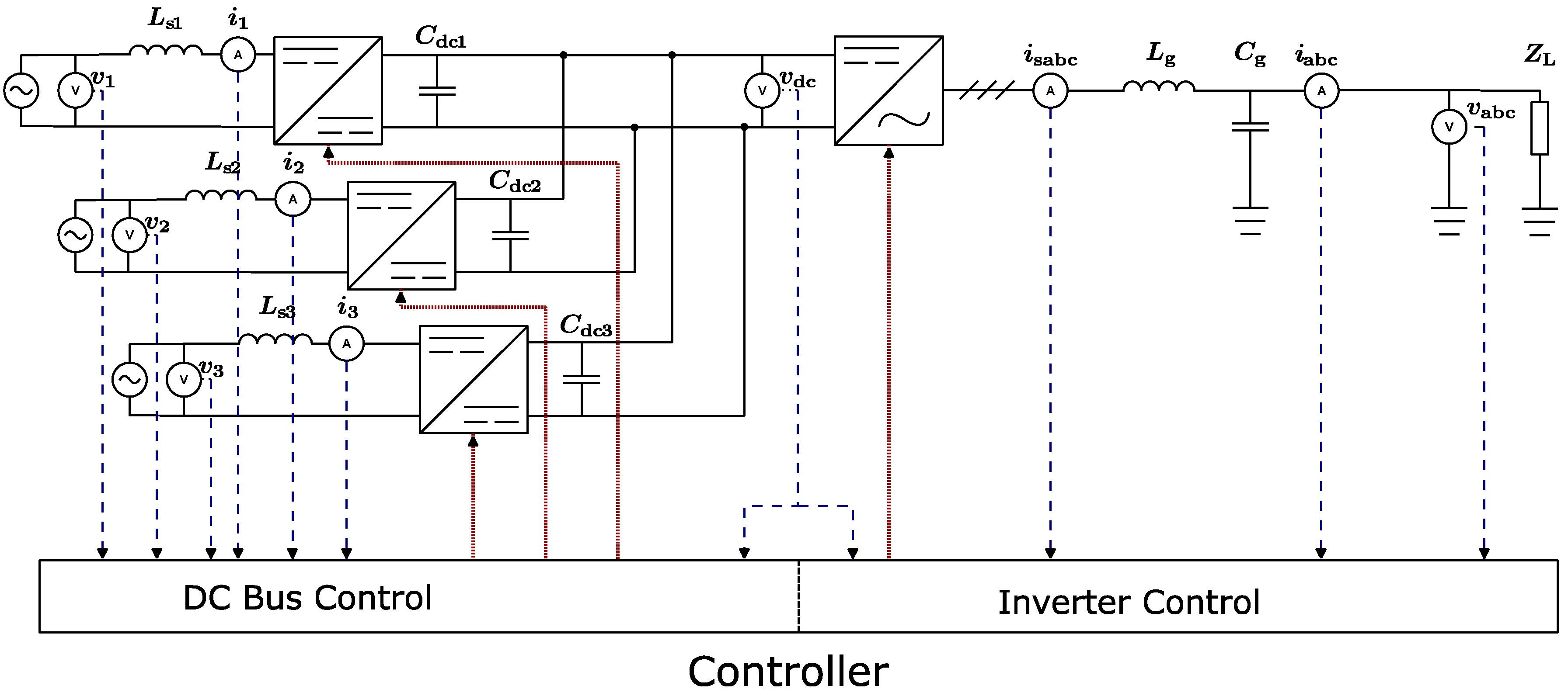
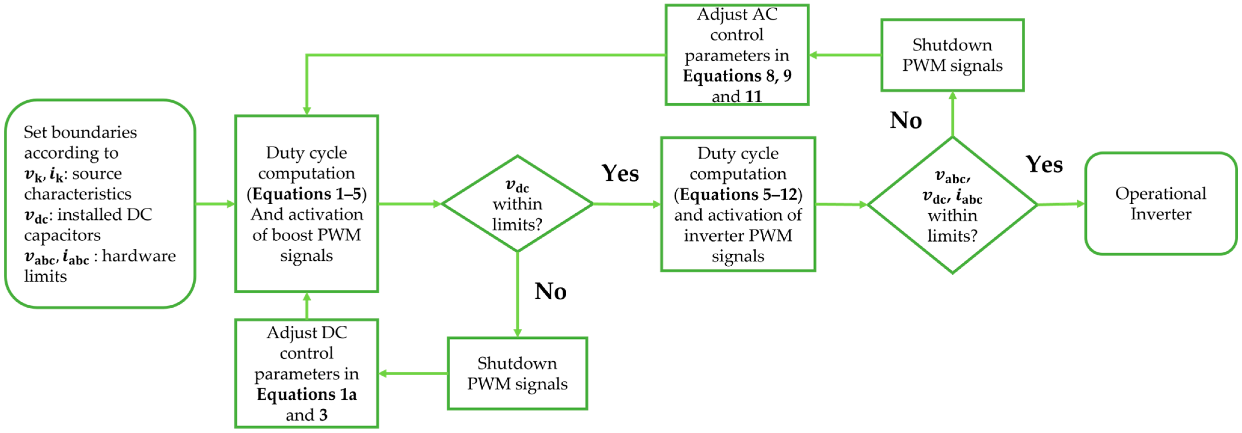
The controller described in Section 2.1 was designed and tested using the software ‘ACG-SDK’ 3.8.0.2 [30] in conjunction with the software ‘Simulink’ 2022a. For initial control functionality tests, a simulation of the plant reflecting the experimental setup and depicted in Figure 2 was run. The plant consists of three parallel DC sources that through a boost converter are each connected to a DC bus. The necessary parameters to be obtained for DC bus control are the DC current, measured behind the source filter L s , and source voltage. The measured values are used to compute the gate signals, which are transmitted to the converters. The voltage conversion is implemented in a three-phase two-level inverter. On the AC side, three single phase loads are connected in a Y-configuration. For the inverter control voltage measurement, units are installed in the DC bus and after the output filter. The inverter switching current is measured before, whereas the grid current is measured behind the output filter. The measured values are fed into the computation of the gate signals for the inverter. The inverter control guarantees functionality of the setup. However, for a reliable and secure operation and safe transition to the experimental phase, adequate shutdown conditions in case of faults need to be defined. The shutdown conditions correspond to limits to AC and DC bus voltages, AC and DC currents, as well as source currents and voltages. Since the system is not connected to the grid, a blackstart procedure has to be defined. The foundation of the blackstart capability of systems like the one in Figure 2 is the ability to charge the DC bus from the DC side. Thus, the initial step is the activation of the boost stage to reach the DC bus reference voltage of 700 V according to Equations (1) to (5). After a delay of 0.5 s, necessary to stabilize the DC bus voltage, the inverter PWM signals that can be derived from Equations (5) to (12). An integrator reset is imperative at the inverter activation stage to remove an accumulated standby error. A stable AC voltage completes the blackstart procedure. During the entire startup procedure, AC and DC side constraints, hard and soft, are operative and effective. Soft constraints at the DC and AC side correspond to the controller output currents that are limited according to the implemented hardware. Hard constraints correspond to situations that can damage the devices or are otherwise not desirable. At the DC side, the source voltages need to be within certain thresholds for the system to operate. At the AC side, overvoltage and overcurrent protections are installed. If any of the hard constraints are violated, the PWM signals of the converter and inverter are shut down and the system enters the error state (Figure 3).
The parameters used for the controller design are listed in Table 1. The underlined values are variable and correspond to the DC bus and inverter control, whereas the remaining values are fixed since they are determined with the hardware used in the experimental setup.

2.3. Experimental Setup

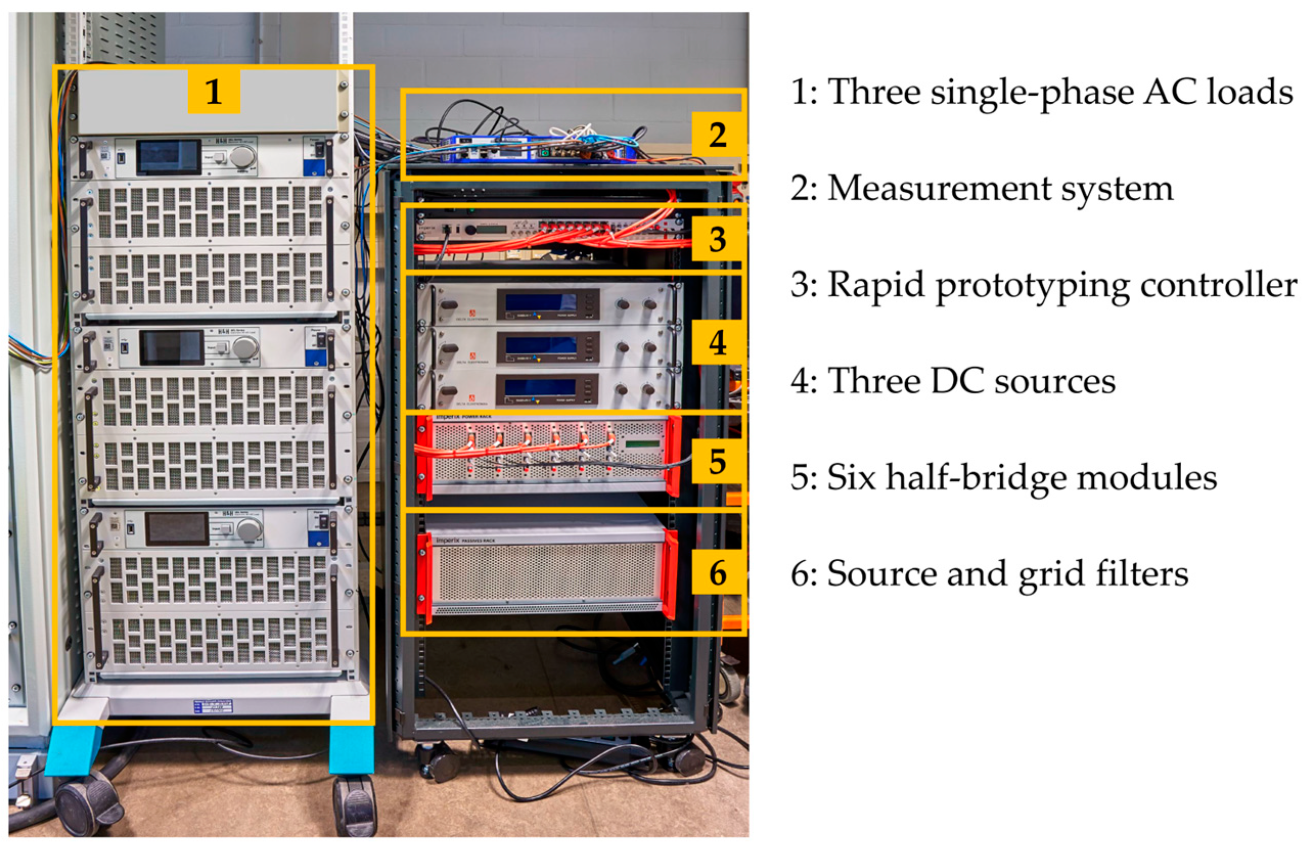
The experimental plant is set up in island configuration (Figure 4). As DC voltage sources, three SM3300 are used and connected in parallel [30]. For each source, a PEB8038 power module is used as the boost stage [31]. The DC/AC stage consists of three PEB8038 power modules operated in conjunction as a two-level three-phase inverter. At the AC side, three ACLS8450 single phase loads are connected in a Y-configuration and operated in the constant resistance mode [32]. Preceding the sources, an inductance serves as a source filter. At the point of the inverter output, grid inductances, capacitances, and an EMC filter are installed.
All current and voltage values necessary for the controller (Figure 2) are either measured with the internal power module measurement devices or with installed DIN-800V and DIN-50A sensors [33,34]. Long-term measurements and calibration of the sensors were performed using a TRIONet. A rapid control prototyping (RCP) system gathers all measurement data and implements the control designed in Section 2.2 [35]. This is carried out by programming the RCP using the code generation function of ACG-SDK.

2.4. System Validation

In order to evaluate and validate the control method, experimental tests are divided into four categories related to blackstart, stationary behavior, transient behavior, and a sensitivity analysis. During all experiments, the AC loads are operated in the constant resistance mode.

2.4.1. Blackstart

The most basic functionality that the system shall feature is the ability to blackstart. Since load conditions for a blackstart differ between different fields of application, it is imperative to verify the blackstart capability under different load conditions. Hence, the boundary cases of 236 Ω (900 W) and 23 Ω (7 kW) phase resistance are tested. These two cases are chosen since they demonstrate the maximum difference in the output current after the inverter PWM signals are activated and thus the difference in stress applied to the DC bus voltage control after startup. Additionally, a zero-load test is performed as well as an intermediate test with 40 Ω phase resistance (4 kW) to verify that a response in-between the boundary cases is obtained. The blackstart is performed according to the process described in Section 2.2. For the DC bus voltage control performance assessment, v d c is used, which is measured at the sensor located between the converter and inverter.
To assess stable operation after startup, the AC voltage, current envelopes, and grid voltages’ dq-values are evaluated. Therefore, v a b c and i a b c are measured, which correspond to the measurements taken behind the grid output filter (Figure 2).

2.4.2. Stationary Behavior

The minimum requirement for a blackstart-capable system is the ability to supply a load indifferent to its magnitude as long as it lies between defined boundaries. The system under investigation is operated as a voltage source. Hence, the power quality needs to be sufficiently good (THD < 1%) in all admissible operating points.
The boundary cases of the system are defined as 236 Ω phase resistance analogous to the minimum load (900 W) and 23 Ω maximum phase resistance (7 kW). To assess the power quality over the full operating range, measurements are taken in steps of 1 kW ranging from 1 to 7 kW. After every step, a settling time of 1 minute is enforced. The power quality is assessed by calculating the THD values of the measured grid voltages v a b c behind the output filters (Figure 2). The THD values are averaged over a 1 s time frame. Additionally, i a b c and v a b c waveforms as well as v d c are measured for the 23 Ω phase resistance case after reaching a steady state to observe voltage and current imbalances.

2.4.3. Transient Behavior

Transient events to evaluate the control system’s performance are tested next. The control system has to stabilize the system under various load transients. This is achieved by an instantaneous adjustment of control effort according to measurement values. As the system under investigation is nonlinear, different initial states have to be taken into account during transient events. Three sets of load transients are measured. The first set comprises a transition from minimum to maximum load in two separate steps. The second set includes two separate steps from medium to maximum load. The final set contains a single step from minimum to maximum load, which mimics the harshest possible transient the system can experience. The detailed load parameters for each separate measured transient are depicted in Table 2. Aiming to grasp the full transient response, the grid output voltages v a b c and currents i a b c along with v d c are measured with a sample frequency of 200 kHz. Additionally, the grid current and voltage dq-values are calculated to evaluate the response. The output active and reactive power values are measured with a 50 Hz sample rate to compare the output to the expected values.

2.4.4. Sensitivity Analysis

Finally, a systematic sensitivity analysis is conducted. The aim is to improve the system’s performance via tuning a selected set of control parameters. However, exactly which parameter or set of parameters to be tweaked to yield the largest improvement has to be determined first. From the source to the load, seven PI controllers are installed, resulting in an aggregate of 14 control parameters. Since the inverter is operated as a voltage source in the island mode, the voltage power quality is essential.
Thus, the voltage controllers according to Equation (9) need to be considered as is the case for the DC bus voltage control, since the nature of matching control implies a connection between v d c and frequency. Consequently, six parameters, two for the DC bus voltage, two for v d , and two for v q , are evaluated. Initial estimates for the controller values were derived heuristically during the simulation stage (Table 1).
The highest stress the DC bus voltage controller can experience occurs during the initial activation of the converters. During this process, the source voltage of 300 V is converted up to 700 V at the DC bus followed by the activation of the inverter. Accordingly, a set of PI parameter permutations for testing is defined to gain insights into the link between parameter alteration and system response. The set of PI values corresponds to the initial values and a 25% deviation in both directions. This results in nine possible combinations (Table 3, 1st Iteration).
The parameter performance is evaluated according to the v d c -overshoot after the boost activation ( v d c m a x ), v d c -drop after inverter activation ( v d c m i n ) , and rising time until 70% of the reference value is reached ( Δ T 580 ). After suitable parameters have been acquired in a first scan, a second set of five tests is conducted. In this set, the first test uses the suitable parameters but increased by 25%. The following four tests amplify that deviation by another 25% with respect not to the initial value but to the value used in the preceding test (Table 3, 2nd Iteration).
The event chosen to stress AC voltage stability is a deliberately introduced pulse offset disturbance in the voltage measurement. Thus, three different effects can be evaluated: (i) the initial response to the pulse, (ii) error minimization during the pulse, and (iii) the response to the inversed offset after the pulse has ended. A key parameter for comparable transient events is the switching time. Thus, a delayed pulse is injected at a rising zero crossing of the first phase of v a b c . The delay is chosen for the pulse to hit at a positive peak of the first phase. The alternated measurements are v d and v q that are perturbed by −15 and −7.5 V, respectively. The pulse duration is set to a full period (20 ms). Changes in the controller’s four parameters are made in all possible combinations by 25% with respect to the initial values (Table 1), resulting in a set, including the nominal case, of 17 tests (Table 4). All tests are performed with a phase resistance of 110 Ω.

3. Laboratory Validation

The following section presents the results of the system validation comprising the investigation of the DC bus voltage control and inverter activation during blackstart for different load conditions, evaluation of stationary behavior at different operating points, transient performance for varying load transitions, as well as a systematic sensitivity analysis aiming to assess links between control parameter alteration and system performance.

3.1. Blackstart

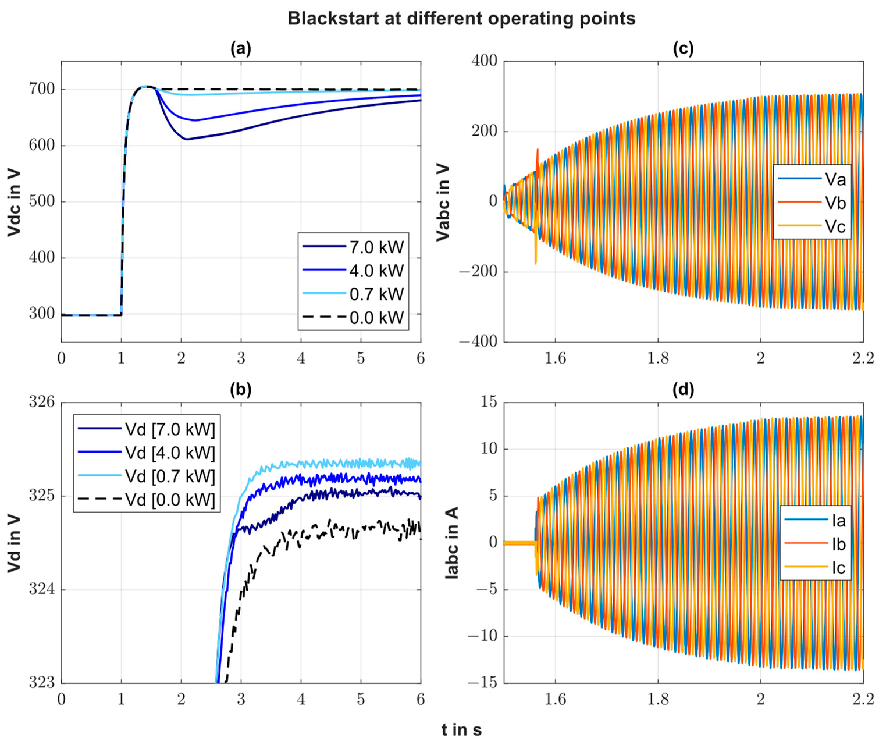
The first phase of the blackstart sees the initialization of the boost stage at t b o o s t = 1   s and an increase in the DC bus voltage at 300 V (source voltage) to 700 V (Figure 5a). This stage is completely decoupled from the AC stage and is only dependent on the DC bus control parameters. Thus, for all observed cases up to the inverter activation time t i n v = 1.5   s , the DC bus responses are indistinguishable. Only after t i n v do differences in the response corresponding to the load conditions begin to materialize. For the minimum load case, the stress on the DC bus causes a drop by 10 V (1.4%) from 700 V to 690 V that is quickly recovered from. In the maximum load case, a drop of 90 V (12.9%) to 610 V is observed that takes longer to recover from. For the medium load case, a response between both cases is observed, confirming a plausible operation of the system.
For the zero-load case, 700 V is maintained. According to Equation (7), the AC voltage angle properties and DC bus voltage are linked. Thus, the different strain is reflected at the AC side (Figure 5b).
The initial response of v d is similar since equal control parameters are used. However, v d still features clear offsets from the reference voltage that in their extent depend on the load conditions. The response mirrors the v d c case leading to a low settling time for minimum load, and a long settling time for the maximum load case at the AC side. The medium lies betwixt both cases, again demonstrating the validity of the system. What is interesting to note is that the zero-load case shows a permanent offset in its AC voltage even though the DC bus performance is ideal. However, this is expected since the performance of power electronic converters can suffer at zero-load conditions due to conversion losses.
In Figure 5c,d, the AC voltage and current waveforms from initial to stable operation are depicted. It is evident that the AC voltage builds up starting from t i n v , as it corresponds to the inverter PWM signal activation. Additionally, the requirement of generating a stable 230 V AC voltage is met.

3.2. Stationary Behavior

To ensure stable steady state operation, the system was tested under different load conditions. Under all load conditions, the output voltage exhibits superb quality with THD values below 1% (Figure 6a). This shows that the system is capable of operating long-term in steady state conditions. The best THD performance is observed in the 3 kW region. The offset between THD for different operating points occurs due to the nonlinearity of the system and is coupled to the chosen control parameters. For all measurements, the parameters were chosen according to Table 1.
In Figure 6b, the DC bus voltage during stationary operation is depicted. A slight deviation from the reference value of 700 V is observed due to an offset between the sensor used for the inverter control and the one used for the long-term data acquisition.
In steady state operation, clean AC voltage and current waveforms can be observed for the maximum load case (Figure 6c,d).

3.3. Transient Behavior

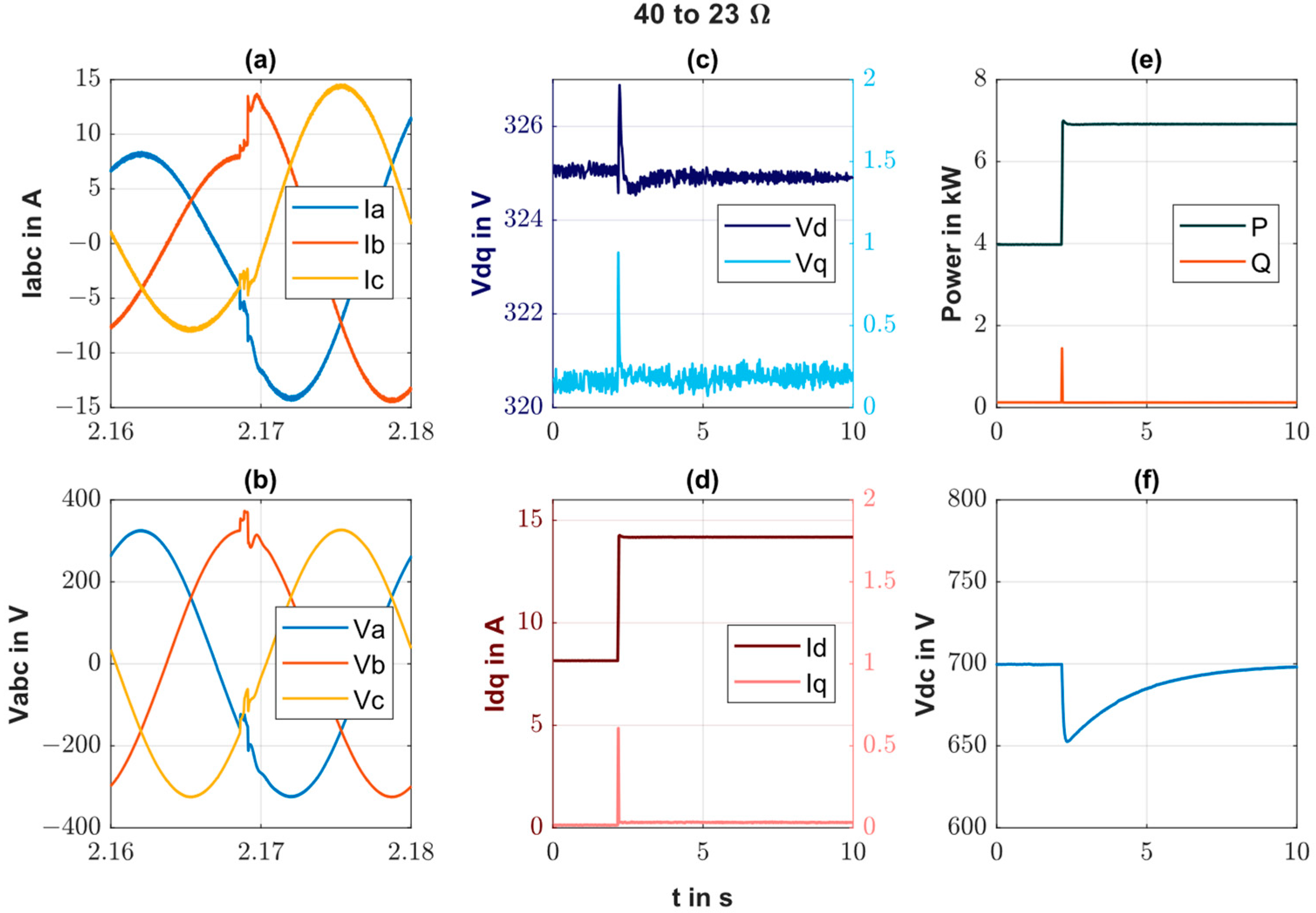
Any large disturbance can push the system to instability. Hence, the ability of the controller to maintain stability in such situations must be verified. To do so, the load transitions listed in Table 2 were performed. Boundaries that are set corresponding to the initial step in Figure 3 and are essential for the transient performance are the limits on v a b c and v d c . An upper limit of 450 V for the amplitude and a safe region of operation between 600 and 800 V are chosen for v a b c and v d c , respectively. For all five load transients, the two voltage values were kept within the defined boundaries, and the THD values measured in Section 3.2 are fully regained in the steady state. For the transient from 40 to 23 Ω (4 to 7 kW), voltage and current waveforms are depicted in Figure 7a,b. A transient induces a slight disturbance in the waveforms that quickly recovers within a few milliseconds. However, the voltage dq-values show an offset beyond the waveform recovery time (Figure 7c). The current dq-values feature a fast response and low settling time after the transient. The active power supplied to the load is stable, but the reactive power shows a spike at the transient that settles fast (Figure 7d). The transient causes a voltage drop in the DC bus that shows a similar response time to the dq-voltages (Figure 7f). Consequently, the transient evaluation shows that the current cascade performance is satisfactory, but raises the possibility to improve the DC and AC voltage control performance. This matches with the results in Section 3.1 and is tackled in the following section.

3.4. Sensitivity Analysis

The aim of the sensitivity analysis is an improvement in performance as well as the evaluation of the control parameters’ effects on the system’s performance, especially the DC bus and AC voltage response.
The need for this is underlined by the results of Section 3.1 and Section 3.3 that depict a poor, i.e., high, settling time for both control values. Consequently, the controllers owning those values are suitable candidates for improvement.

3.4.1. Sensitivity DC Bus Voltage Controller

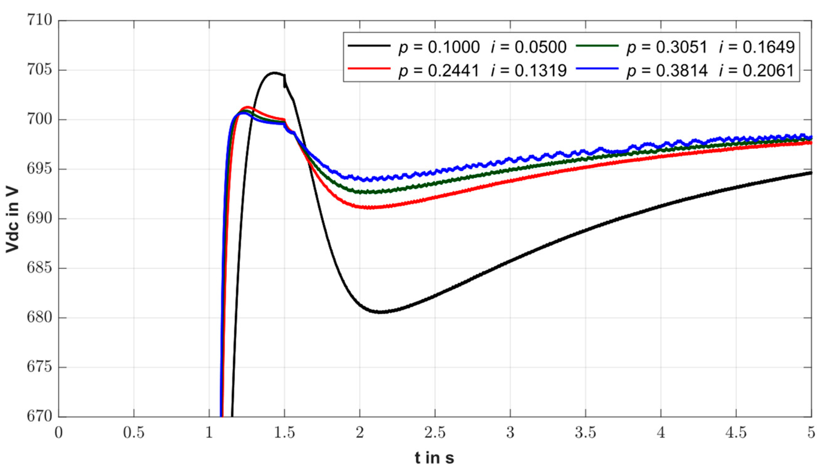
For the first iteration of experiments, all possible combinations corresponding to a 25% offset from the initial PI parameters are evaluated. The values and their corresponding response to a boost operation from the initial value of 300 to 700 V are depicted in Table 3. The voltage v d c m a x corresponds to the maximum voltage overshoot as a cause of the converter activation at t b o o s t (1 s). The voltage v d c m i n corresponds to the voltage drop after the inverter activation at t i n v (1.5 s). Δ T 580 is the time period that it takes for the DC bus voltage to rise to 70% of its reference value starting from t b o o s t . For all tests with a constant p of 0.075 (Tests 1–3), an increase in parameter i will have the two desirable effects of a lower response time and a less pronounced voltage drop after t i n v , but also the unwanted effect of an increased overshoot following the largest voltage step at t b o o s t . As a result, a trade-off between a sufficiently low response time (accompanied by a sufficiently small voltage drop) and an acceptable overshoot has to be found. All three cases show poor performance in the voltage overshoot and drop as well as rise time compared to the initial PI values (Test 5). Setting the p parameter to the initial value and varying the i value (Tests 4–6) demonstrates the same characteristic with no apparent improvement in the evaluation parameters. Raising the p value to 0.125 and varying the i parameter show promising results (Tests 7–9). All three cases outperform the nominal case in v d c m a x , v d c m i n , and Δ T 580 . The tests share a similar rise time and mostly differ in the voltage overshoot and drop. Analogous to the previous six tests, the trade-off corresponding to an increasing i parameter continues. The overshoot corresponds to a unique event that is only affected by DC side parameters. Contrarily, the voltage drop is linked to a switching event that is repetitive during operation and is affected by AC and DC side parameters. Thus, a lower v d c m i n value is preferred. Test 9 satisfies these conditions. Since the first scan revealed that increases rather than decreases in both control parameters by 25% yielded better results, a second set of five tests were conducted, further increasing the PI parameters (Tests 10–14). Each successive test leads to better v d c m i n and v d c m a x values but stagnant Δ T 580 values. However, although these results look promising, the observation of responses of the DC bus voltages over time for the three bests results (Tests 12–14) and the nominal case paints a somewhat different picture (Figure 8).
Test 14 shows the best performance according to the evaluation parameters, but induces oscillations in v d c .
Thus, the best compromise between good evaluation values, and the v d c response is obtained with the parameters of Test 13 that shows a better performance compared to the nominal values while also displaying reduced oscillations.

3.4.2. Sensitivity of the AC Voltage Controller

The task of the voltage controllers is to keep v d and v q close to their reference values of 325 and 0 V, respectively. In total, four PI parameters are permuted in a set of 16 tests, depicted in Table 4. A pulse disturbance (20 ms) of −15 and −7.5 V is injected into the digital v d and v q measurements, respectively. The injection takes place at a peak in the first phase of v a b c . Oscillation after disturbance, settling time, offset, and THD are chosen as evaluation parameters. The first observation is that only the p values are potent enough to affect the system’s performance when changed only slightly, whereas other parameters need more tweaking to have a relevant influence on the system. No noticeable change is induced by any permutation of the i value. The most promising cases are Tests 2 and 12 (Figure 9a). Test 2 corresponds to an increase in both p values by 25% and shows fewer oscillations as well as less overshoot. However, the decreased overshoot at the end of the pulse is due to the high settling time that restored v d to 317 V only. Additionally, Test 12 outperforms Test 2 at THD with 0.333% compared to 0.381%. However, since oscillations are not desirable, two additional tests are conducted, in which p is successively reduced by 25% per test compared to Test 2 (Table 5, 2nd Set). In Figure 9b, the effect of consistently reducing the p values can be observed. Compared to the nominal value, the oscillations are reduced, but in return higher THD values of 0.42 and 0.5% are obtained for Tests 17 and 18, respectively. Test 18 shows a poorer performance compared to all evaluated cases since only in this test the disturbance is not being compensated for but rather an additional offset is observed ending at 305 V. Additionally, Test 18 displays a higher settling time as a recovery to only 313 V is observed near the end of the pulse as compared to 316 V for Test 17.
A trade-off can be reached by increasing the i value repetitively and keeping the p values as high as possible. A third set of tests were conducted with a dramatic increase in i and alternating p values in order to find a compromise between oscillations and THD (3rd Set). In Figure 9c, the nominal case and the third set are depicted. For Tests 21 and 22, the voltage reaches the reference value by the end of the pulse, demonstrating fast disturbance recovery compared to the other tests. Similar to the results in the first 16 tests, the offset compared to the nominal value is attributed to the fast response. It is noteworthy that the voltage profile exhibits oscillations while the pulse is active as the systems try to compensate for the disturbance. The amplitude increases with decreasing p and increasing i values. Thus, the compromise that encompasses a fast response, low oscillations in disturbed state, and low oscillations after the disturbance are the parameters of Test 21.

4. Conclusions and Outlook

There are various methods to control grid-forming inverters. Regardless of the type and method of control, these controllers usually are designed in software environments and their parameters are calculated by simulation. However, caused by the unavoidable presence of non-ideal behavior in physical hardware systems mainly due to parasitic elements, the control system that worked fine in a simulation environment may reveal flaws in its performance after uploading the control software onto the inverter hardware. Hence, fine-tuning of the controller parameters increases the control system performance. Providing the means to do so via matching control in a systematic and highly reproducible manner by employing a sensitivity analysis is the core contribution of the present work.
Firstly, a detailed controller synthesis comprising the DC bus voltage control, matching grid-forming control, and necessary state machine was presented. Secondly, a detailed plant description including necessary measurements and a validation procedure is introduced, aiming to assess and improve the investigated system in stand-alone operation. Finally, the experiments based on a sensitivity analysis were conducted, which yielded the following results:
The study shows that the tuned system can successfully perform a blackstart in various initial loading conditions. Notably, the inverter exhibits consistent and reliable performance across these test scenarios. In the steady state operation, the inverter maintained a total harmonic distortion (THD) of less than 0.5% over most of its loading range. In transient performance tests, which assessed the overshoot and settling time and oscillatory behavior, the inverter demonstrated satisfactory stability, indicating its capability to respond effectively to step load changes. These results underscore the viability and effectiveness of the studied grid-forming inverter in the integration of renewable energy resources in stand-alone power systems and microgrids. The proposed method is deemed superior to the currently employed trial-and-error approach and is thus suggested to be used instead.
Future work will focus on the interaction of the presented laboratory setup with grid-following and supporting inverters. In addition, it will be of great interest to substitute the currently used DC sources with laboratory-scale fuel cells.

Author Contributions

Conceptualization, E.D.G.A. and K.P.; methodology, E.D.G.A. and K.P.; software, E.D.G.A.; validation, E.D.G.A. and K.P.; formal analysis, K.P.; investigation, K.P.; resources, D.B.; data curation, E.D.G.A.; writing—original draft preparation, E.D.G.A. and K.P.; writing—review and editing, D.S. and D.B.; visualization, D.B.; supervision, D.S.; project administration, D.B. and E.D.G.A.; funding acquisition, D.S. All authors have read and agreed to the published version of the manuscript.

Funding

This research paper is funded by dtec.bw—Digitalization and Technology Research Center of the Bundeswehr—which we gratefully acknowledge. dtec.bw is funded by the European Union—NextGenerationEU.

Data Availability Statement

Data supporting this study are openly available at https://zenodo.org/records/10389957 (accessed on 6 December 2023).

Conflicts of Interest

The authors declare no conflict of interest.

Abbreviations

The following abbreviations are used in the text:
DPCDirect power control
GFLIGrid-following inverter
GFMIGrid-forming inverter
RCPRapid control prototyping
THDTotal harmonic distortion
VOCVirtual oscillator control
VSMVirtual synchronous machine

References

  1. Rocabert, J.; Luna, A.; Blaabjerg, F.; Rodríguez, P. Control of Power Converters in AC Microgrids. IEEE Trans. Power Electron. 2012, 27, 4734–4749. [Google Scholar] [CrossRef]
  2. Rosso, R.; Wang, X.; Liserre, M.; Lu, X.; Engelken, S. Grid-Forming Converters: Control Approaches, Grid-Synchronization, and Future Trends—A Review. IEEE Open J. Ind. Appl. 2021, 2, 93–109. [Google Scholar] [CrossRef]
  3. Rosso, R.; Wang, X.; Liserre, M.; Lu, X.; Engelken, S. Grid-forming converters: An overview of control approaches and future trends. In Proceedings of the 2020 IEEE Energy Conversion Congress and Exposition (ECCE), Detroit, MI, USA, 11–15 October 2020; pp. 4292–4299. [Google Scholar]
  4. Wang, X.; Taul, M.G.; Wu, H.; Liao, Y.; Blaabjerg, F.; Harnefors, L. Grid-Synchronization Stability of Converter-Based Resources—An Overview. IEEE Open J. Ind. Appl. 2020, 1, 115–134. [Google Scholar] [CrossRef]
  5. D’Arco, S.; Suul, J.A. Virtual synchronous machines—Classification of implementations and analysis of equivalence to droop controllers for microgrids. In Proceedings of the 2013 IEEE Grenoble Conference, Grenoble, France, 16–20 June 2013; pp. 1–7. [Google Scholar]
  6. Lasseter, R.H.; Chen, Z.; Pattabiraman, D. Grid-Forming Inverters: A Critical Asset for the Power Grid. IEEE J. Emerg. Sel. Top. Power Electron. 2020, 8, 925–935. [Google Scholar] [CrossRef]
  7. Unruh, P.; Nuschke, M.; Strauß, P.; Welck, F. Overview on Grid-Forming Inverter Control Methods. Energies 2020, 13, 2589. [Google Scholar] [CrossRef]
  8. Anttila, S.; Döhler, J.S.; Oliveira, J.G.; Boström, C. Grid Forming Inverters: A Review of the State of the Art of Key Elements for Microgrid Operation. Energies 2022, 15, 5517. [Google Scholar] [CrossRef]
  9. Zhang, H.; Xiang, W.; Lin, W.; Wen, J. Grid Forming Converters in Renewable Energy Sources Dominated Power Grid: Control Strategy, Stability, Application, and Challenges. J. Mod. Power Syst. Clean Energy 2021, 9, 1239–1256. [Google Scholar] [CrossRef]
  10. Rathnayake, D.B.; Akrami, M.; Phurailatpam, C.; Me, S.P.; Hadavi, S.; Jayasinghe, G.; Zabihi, S.; Bahrani, B. Grid Forming Inverter Modeling, Control, and Applications. IEEE Access 2021, 9, 114781–114807. [Google Scholar] [CrossRef]
  11. Mahmoud, K.; Astero, P.; Peltoniemi, P.; Lehtonen, M. Promising Grid-Forming VSC Control Schemes Toward Sustainable Power Systems: Comprehensive Review and Perspectives. IEEE Access 2022, 10, 130024–130039. [Google Scholar] [CrossRef]
  12. de Brabandere, K.; Bolsens, B.; van den Keybus, J.; Woyte, A.; Driesen, J.; Belmans, R. A Voltage and Frequency Droop Control Method for Parallel Inverters. IEEE Trans. Power Electron. 2007, 22, 1107–1115. [Google Scholar] [CrossRef]
  13. Beck, H.-P.; Hesse, R. Virtual synchronous machine. In Proceedings of the 2007 9th International Conference on Electrical Power Quality and Utilisation (EPQU 2007), Barcelona, Spain, 9–11 October 2007; pp. 1–6. [Google Scholar]
  14. Li, C.; Burgos, R.; Cvetkovic, I.; Boroyevich, D.; Mili, L.; Rodriguez, P. Analysis and design of virtual synchronous machine based STATCOM controller. In Proceedings of the COMPEL: 2014 IEEE 15th Workshop on Control and Modeling for Power Electronics, Santander, Spain, 22–25 June 2014; pp. 1–6. [Google Scholar]
  15. Seo, G.-S.; Colombino, M.; Subotic, I.; Johnson, B.; Gros, D.; Dorfler, F. Dispatchable Virtual Oscillator Control for Decentralized Inverter-dominated Power Systems: Analysis and Experiments. In Proceedings of the APEC 2019: Thirty-Fourth Annual IEEE Applied Power Electronics Conference, Anaheim, CA, USA, 17–21 March 2019; pp. 561–566. [Google Scholar]
  16. Shi, Z.; Li, J.; Nurdin, H.I.; Fletcher, J.E. Comparison of Virtual Oscillator and Droop Controlled Islanded Three-Phase Microgrids. IEEE Trans. Energy Convers. 2019, 34, 1769–1780. [Google Scholar] [CrossRef]
  17. Johnson, B.B.; Sinha, M.; Ainsworth, N.G.; Dorfler, F.; Dhople, S.V. Synthesizing Virtual Oscillators to Control Islanded Inverters. IEEE Trans. Power Electron. 2016, 31, 6002–6015. [Google Scholar] [CrossRef]
  18. Raisz, D.; Thai, T.T.; Monti, A. Power Control of Virtual Oscillator Controlled Inverters in Grid-Connected Mode. IEEE Trans. Power Electron. 2019, 34, 5916–5926. [Google Scholar] [CrossRef]
  19. Yu, H.; Awal, M.A.; Tu, H.; Husain, I.; Lukic, S. Comparative Transient Stability Assessment of Droop and Dispatchable Virtual Oscillator Controlled Grid-Connected Inverters. IEEE Trans. Power Electron. 2021, 36, 2119–2130. [Google Scholar] [CrossRef]
  20. Lu, M.; Dutta, S.; Purba, V.; Dhople, S.; Johnson, B. A Grid-compatible Virtual Oscillator Controller: Analysis and Design. In Proceedings of the 2019 IEEE Energy Conversion Congress and Exposition (ECCE), Baltimore, MD, USA, 29 September–3 October 2019; pp. 2643–2649. [Google Scholar]
  21. Ndreko, M.; Rüberg, S.; Winter, W. Grid forming control scheme for power systems with up to 100% power electronic interfaced generation: A case study on Great Britain test system. IET Renew. Power Gener. 2020, 14, 1268–1281. [Google Scholar] [CrossRef]
  22. Huang, L.; Xin, H.; Wang, Z.; Wu, K.; Wang, H.; Hu, J.; Lu, C. A Virtual Synchronous Control for Voltage-Source Converters Utilizing Dynamics of DC-Link Capacitor to Realize Self-Synchronization. IEEE J. Emerg. Sel. Top. Power Electron. 2017, 5, 1565–1577. [Google Scholar] [CrossRef]
  23. Jouini, T.; Arghir, C.; Dörfler, F. Grid-Friendly Matching of Synchronous Machines by Tapping into the DC Storage. IFAC-Pap. 2016, 49, 192–197. [Google Scholar] [CrossRef]
  24. Cvetkovic, I.; Boroyevich, D.; Burgos, R.; Li, C.; Mattavelli, P. Modeling and control of grid-connected voltage-source converters emulating isotropic and anisotropic synchronous machines. In Proceedings of the 2015 IEEE 16th Workshop on Control and Modeling for Power Electronics (COMPEL), Vancouver, BC, Canada, 12–15 July 2015; pp. 1–5. [Google Scholar]
  25. Milano, F.; Dorfler, F.; Hug, G.; Hill, D.J.; Verbic, G. Foundations and Challenges of Low-Inertia Systems (Invited Paper). In Proceedings of the PSCC: 2018 Power Systems Computation Conference, Dublin, Ireland, 11–15 June 2018; pp. 1–25. [Google Scholar]
  26. Qoria, T.; Gruson, F.; Colas, F.; Guillaud, X.; Debry, M.-S.; Prevost, T. Tuning of Cascaded Controllers for Robust Grid-Forming Voltage Source Converter. In Proceedings of the 2018 Power Systems Computation Conference (PSCC), Dublin, Ireland, 11–15 June 2018. [Google Scholar] [CrossRef]
  27. Wu, H.; Wang, X. Small-Signal Modeling and Controller Parameters Tuning of Grid-Forming VSCs With Adaptive Virtual Impedance-Based Current Limitation. IEEE Trans. Power Electron. 2022, 37, 7185–7199. [Google Scholar] [CrossRef]
  28. Arghir, C.; Jouini, T.; Dörfler, F. Grid-forming control for power converters based on matching of synchronous machines. Automatica 2018, 95, 273–282. [Google Scholar] [CrossRef]
  29. Tayyebi, A.; Gross, D.; Anta, A.; Kupzog, F.; Dorfler, F. Frequency Stability of Synchronous Machines and Grid-Forming Power Converters. IEEE J. Emerg. Sel. Top. Power Electron. 2020, 8, 1004–1018. [Google Scholar] [CrossRef]
  30. Davidse, L. SM3300_DTS_V202306. Available online: https://www.delta-elektronika.nl/sites/default/files/2023-06/SM3300_DTS_V202306.pdf (accessed on 15 September 2023).
  31. Imperix, PEB8038—Half-Bridge SiC Power Module. Available online: https://cdn.imperix.com/wp-content/uploads/document/PEB8038.pdf (accessed on 15 September 2023).
  32. Höcherl & Hackl, ACLS8450—Elektronische AC Last—Höcherl & Hackl. Available online: https://www.hoecherl-hackl.de/produktangebot/acls8450/ (accessed on 15 September 2023).
  33. DIN-50A. Available online: https://cdn.imperix.com/wp-content/uploads/document/DIN-50A.pdf (accessed on 15 September 2023).
  34. DIN-800V. Available online: https://cdn.imperix.com/wp-content/uploads/document/DIN-800V.pdf (accessed on 15 September 2023).
  35. Imperix Ltd. B-Box RCP Datasheet. Available online: https://cdn.imperix.com/wp-content/uploads/document/B-Box_Datasheet.pdf (accessed on 15 September 2023).
Figure 1. Three control cascades consisting of grid-forming stage (A), voltage control stage (B), and current control stage (C).
Energies 16 08079 g001
Figure 2. Sketch of laboratory plant and controller input measurements (dashed) and gate outputs (dotted).
Energies 16 08079 g002
Figure 3. Flowchart of the proposed controller synthesis process. The first stage focuses on providing a dc bus voltage that respects the boundaries during stationary operation. The second stage uses the stable dc bus voltage as a foundation to generate AC quantities that remain in the boundaries during operation. Breaching the boundaries leads to a shutdown of both DC and AC generation stages. The process is initiated in offline simulations to derive suitable initial conditions for the transition to the experimental phase. After completion, the code is uploaded to the physical controller and the process is repeated in the experimental setup.
Energies 16 08079 g003
Figure 4. Experimental setup of the island case for the controller validation.
Energies 16 08079 g004
Figure 5. Effect of the blackstart procedure on the DC bus voltage (a) and AC voltage d-component (b) under different initial load conditions and the AC voltage (c) and current (d) waveforms for the 7 kW case.
Energies 16 08079 g005
Figure 6. Stationary characteristics of the system. The voltage THD values (1 s average) are evaluated over the range of 1 to 7 kW for each phase (a). The DC bus voltage (b), grid voltage (c), and grid current (d) are stable during stationary application.
Energies 16 08079 g006
Figure 7. Transient and long-term behavior during a load step from 40 to 23 Ω (4 to 7 kW). Transient behavior is evaluated during an observation period of 20 ms for grid current and voltage (a,b). The grid voltage dq-components (c) and DC bus voltage (f) show a similar response time, as they are linked. Grid current dq-components and power (d,e) show a low settling time.
Energies 16 08079 g007
Figure 8. DC bus voltage response after a blackstart at 1 s and inverter activation at 1.5 s for increasing DC bus voltage control PI parameters.
Energies 16 08079 g008
Figure 9. Response of v d to a −15 V pulse disturbance with a duration of 20 ms. Plot (a) depicts a comparison of the nominal value (Test 0) and tests with a 25% increase (Test 12) and decrease (Test 2) in the p parameter of the voltage cascade. In plot (b), a second set with further decreases in successive tests is depicted. In (c), i has been increased dramatically in Tests 21 and 22.
Energies 16 08079 g009
Table 1. Variable (underlined) and fixed controller parameters.
DC Bus Control
DC bus voltage v d c 700 VDC bus capacitance C d c 1 / 2 / 3 1 mF
Source voltage v 1 3 300 VVoltage control P/I k p d c / k i d c 0.1/0.05
Source filter L s 1 / 2 / 3 2.2 mHCurrent control P/I k p b / k i b 12.5/110
Switching frequency f s 20 kHzDC current limit i d c m a x * 25 A
Inverter Control
Grid inductance L g 2.2 mHVoltage magnitude control P/I k p v m / k i v m 0.1/5
Grid capacitance C g 100 mFd-current control P/I k p i d / k i i d 6.25/55
Load range Z L 1–7 kWq-current control P/I k p i q / k i i q 12.5/110
AC current limit i s k m a x * 30 Ad-voltage control P/I k p v d / k i v d 0.25/1
AC voltage reference v m * 230 2 Vq-voltage control P/I k p v q / k i v q 0.23/1
Angle sensitivity α 0.1257Reference angle frequency ω 0 314 rad/s
Table 2. Transient load steps under investigation.
Initial LoadFinal Load
236 Ω (0.9 kW)40 Ω (4 kW)
40 Ω (4.0 kW)23 Ω (7 kW)
40 Ω (4.0 kW)29 Ω (6 kW)
29 Ω (6.0 kW)23 Ω (7 kW)
236 Ω (0.9 kW)23 Ω (7 kW)
Table 3. Controller PI parameters for the initial (1st iteration) and the expanded tests (2nd iteration).
Test Nr.pi v d c m a x ( V ) v d c m i n ( V ) Δ T 580 ( m s )
1st Iteration
10.0750.0375707.97675.4575.69
20.0750.0500711.00678.1175.14
30.0750.0675714.85680.6574.45
40.1000.0375703.60678.6761.26
50.1000.0500704.75680.4861.49
60.1000.0675706.65681.8961.00
70.1250.0375701.85681.4554.77
80.1250.0500702.73682.6754.69
90.1250.0675703.95684.0854.68
2nd Iteration
100.15620.0844702.50686.8651.25
110.19530.1055701.85689.2649.89
120.24410.1319701.28691.0149.89
130.30510.1649700.93692.5649.89
140.38140.2061700.70693.7949.91
Table 4. AC voltage PI parameters for d and q transformations.
Test Nr. k p v d / k i v d k p v q / k i v q Test Nr. k p v d / k i v d k p v q / k i v q
00.2500/1.000.2300/1.008 (repetition)0.1875/1.250.2875/1.25
10.1875/0.750.1725/0.7590.3125/0.750.1725/0.75
20.1875/0.750.1725/1.25100.3125/0.750.1725/1.25
30.1875/0.750.2875/0.75110.3125/0.750.2875/0.75
40.1875/0.750.2875/1.25120.3125/0.750.2875/1.25
50.1875/1.250.1725/0.75130.3125/1.250.1725/0.75
60.1875/1.250.1725/1.25140.3125/1.250.1725/1.25
70.1875/1.250.2875/0.75150.3125/1.250.2875/0.75
80.1875/1.250.2875/1.25160.3125/1.250.2875/1.25
Table 5. Controller PI parameters for decreasing p (2nd Set) and increasing i (3rd Set).
Test Nr. k p v d k i v d k p v q k i v q THD
2nd Set
170.1400.5620.1291.5620.420
180.1050.4210.0971.9530.500
3rd Set
190.250100.230100.340
200.225100.207100.345
210.225200.207200.345
220.187200.172200.365
Disclaimer/Publisher’s Note: The statements, opinions and data contained in all publications are solely those of the individual author(s) and contributor(s) and not of MDPI and/or the editor(s). MDPI and/or the editor(s) disclaim responsibility for any injury to people or property resulting from any ideas, methods, instructions or products referred to in the content.