Article

Numerical Analysis on the Effect of the Conduction Band Offset in Dion–Jacobson Perovskite Solar Cells

1
School of Physics and Telecommunication Engineering, Yulin Normal University, Yulin 537000, China
2
Office of the Party Committee, Guangxi Minzu Normal University, Chongzuo 532200, China
3
Center for Applied Mathematics of Guangxi, Yulin Normal University, Yulin 537000, China
4
Guangxi Colleges and Universities Key Laboratory of Complex System Optimization and Big Data Processing, Yulin Normal University, Yulin 537000, China
5
Department of Mechanical Engineering, South Dakota State University, Brookings, SD 57007, USA
*
Authors to whom correspondence should be addressed.
Energies 2023, 16(23), 7889; https://doi.org/10.3390/en16237889
Submission received: 25 October 2023 / Revised: 18 November 2023 / Accepted: 30 November 2023 / Published: 2 December 2023
(This article belongs to the Section A2: Solar Energy and Photovoltaic Systems)

Abstract

:
Benefiting from the advantages of a high absorption coefficient, a long charge diffusion length, excellent carrier mobility, and a tunable bandgap, three-dimensional (3D) metal halide perovskites exhibit great potential for application in solar cells. However, 3D perovskite solar cells (PSCs) often suffer from poor long-term stability against moisture, heat, and light. To address this issue, reducing the dimension of perovskite and forming two-dimensional (2D) perovskites can be effective in slowing down the oxidation of the perovskite film and significantly improving device stability. In this study, 2D PSCs were designed with glass/FTO/TiO2/Dion–Jacobson (DJ) perovskite/NiOx/Au structures, based on the solar cell simulation software SCAPS. The absorption layers employed in the study included PeDAMA2Pb3I10, PeDAMA3Pb4I13, PeDAMA4Pb5I16, and PeDAMA5Pb6I19. The influence of the conduction band offset (CBO) variation in the range of −0.5 to 0.5 eV on cell performance was explored through a numerical simulation. The simulation results indicate that the open-circuit voltage and fill factor continue to increase, whereas the short-circuit current density remains almost unchanged when the CBO increases from −0.5 eV to 0 eV. The devices exhibit better performance when the value of the CBO is positive and within a small range. For DJ PSCs, controlling the CBO within 0.1–0.4 eV is conducive to better cell performance.

1. Introduction

As a research direction with great potential in the field of solar cells, the development of perovskite solar cells (PSCs) has experienced rapid growth. The power conversion efficiency (PCE) of PSCs has surged from only 3.8% in 2009 to an impressive 25.73% to 28.75% [1,2,3,4]. Three-dimensional (3D) metal halide perovskites demonstrate substantial promise for solar cell applications owing to their high absorption coefficient, long charge diffusion length, excellent carrier mobility, and tunable bandgap. However, the inherent drawback of 3D PSCs lies in their inferior long-term stability against moisture, heat, and light, limiting their commercial potential. Various strategies, including doping, component engineering, interfacial modification, the use of novel electron and hole transport materials, and encapsulation have been used to enhance the stability of PSCs. Recent studies suggest that reducing the dimension of perovskite and forming 2D perovskites by introducing hydrophobic organic cations [5,6,7] can effectively mitigate the oxidation of the perovskite film, significantly improving device stability. Dion–Jacobson (DJ) perovskite, characterized by a distinct stacked structure, is a common form of 2D perovskite. In DJ perovskites, neighboring inorganic slabs are bridged by diammonium spacers without van der Waals gaps [8]. DJ perovskite PSCs exhibit superior optoelectronic characteristics and enhanced durability [9,10]. Despite these advantages, DJ PSCs face challenges related to serious non-radiative recombination in the bulk [11] and interface, resulting in poor carrier extraction and collection compared to 3D PSCs. Consequently, DJ PSCs still exhibit lower PCEs than their 3D counterparts.
To enhance the performance of DJ perovskite PSCs, numerous strategies have been proposed to optimize film quality, including compositional engineering [11], solvent engineering [12], additive addition [13], and an annealing process [14]. In 2019, Zheng et al. achieved PCEs of 14.16% and 16.38% by employing 1.3-propanediammonium (PDA) and 1.4-butanediammonium (BDA) to construct DJ PSCs, respectively. Their experimental results demonstrated that by controlling the thickness of the quantum well barrier, they could obtain DJ phase perovskites with better orientation and a more uniform distribution, thereby boosting the performance of DJ PSCs [15]. In 2021, Chen and colleagues fabricated DJ PSCs with a gradient energy band alignment in 2021 by coating FABr onto the perovskite films, resulting in an increase in the PCE from 13.78% to 16.75% [16]. Chen et al. also utilized a novel annealing process, combining pre-annealing and merged annealing, to modify the interface at the perovskite and charge-transporting layer, promoting charge transport [17]. To suppress surface defect density, Zhang et al. proposed a secondary anti-solvent strategy for DJ perovskite films which proved effective in preparing highly efficient DJ PSCs [18]. Mohammed et al. demonstrated through a numerical simulation that DJ PSCs with pentamethylenediamine spacers were promising for photovoltaic applications [19]. They optimized different parameters to improve solar cell performance and achieved a PCE of 21.17% [20]. In 2023, Zhai and coworkers proposed that charge recombination could be suppressed, interfacial charge accumulation restricted, and charge transport promoted by introducing an interlayer of polyaspartic acid at the interface of a hole-transporting layer (HTL) and a perovskite layer. With this optimization strategy, the PCE of a DJ PSC increased from 15.03% to 17.34% [21].
Many reported studies have confirmed that the characteristics of the interface between the perovskite layer and carrier transport layers have a direct impact on cell performance. The conduction band offset (CBO) between the perovskite layer and the electron transport layer (ETL) is an important feature of the interface. Therefore, there is a correlation between the CBO and cell performance. A suitable ETL should exhibit proper band alignment with the perovskite layer, ensuring that the transport of electrons is promoted while holes are hindered [22,23,24]. In order to achieve good band alignment between the perovskite layer and ETL, researchers have proposed many methods for interface engineering [25,26], such as doping the ETL with other elements to reach the optimal band alignment with the perovskite layer [22,23], adjusting the band structure via gradient doping [27], inserting a buffer layer between the perovskite layer and the ETL [28], or adjusting the electron affinity of the ETL to achieve proper band matching [29].
DJ PSCs were fabricated by incorporating bulky organic ammonium spacer pentamethylenediamine (PeDA) into DJ perovskite films with four different layer numbers: 3, 4, 5, and 6. These layer numbers correspond to PeDAMA2Pb3I10, PeDAMA3Pb4I13, PeDAMA4Pb5I16, and PeDAMA5Pb6I19, respectively. In this study, DJ PSCs, including PeDA-DAMA2Pb3I10-based PSCs, PeDAMA3Pb4I13-based PSCs, PeDAMA4Pb5I16-based PSCs, and PeDAMA5Pb6I19-based PSCs, were constructed and simulated using a one-dimensional (1D) solar cell simulation program, SCAPS. The focus of this simulation was on assessing the impact of the conduction band offset (CBO) between the DJ perovskite layer and the electron transport layer (ETL). To understand the operation mechanism of the devices, the relationship between the CBO in the range of −0.5 eV to 0.5 eV and the performance of the DJ PSCs was analyzed. The evaluation indicators included the open-circuit voltage (Voc), short-circuit current density (Jsc), fill factor (FF), PCE, recombination current, and recombination rate. The numerical simulation results presented in this article offer significant guidance for the development and manufacturing of highly efficient DJ PSCs and provide a solid foundation for future advancements in solar energy technology.

2. Methods and Materials

2.1. Numerical Research Method

Studying PSCs through a numerical simulation can mitigate the influence of unrelated external factors and help researchers analyze the internal physical mechanisms of PSCs. This approach promotes the development of PSCs in experimental preparation. Therefore, in this study, a 1D numerical simulation software, SCAPS, developed by Professor Burgelman of Gent University in Belgium [30], was adopted as the research tool. SCAPS is widely used for numerical simulations of solar cells. Based on the fundamental equations of semiconductor device physics, including the Poisson equation, hole continuity equations, and electron continuity equations (Equations (1)–(3)) [31,32], SCAPS can calculate the current density–voltage characteristics (J-V), spectral response, capacitance–frequency characteristics (C-F), capacitance–voltage characteristics (C-V) band structures, carrier concentration, and spectral response under specific boundary conditions and has been extensively employed in numerical analyses of perovskite solar cells [3,4,33]. Specific operating parameters such as bias voltage, frequency, and temperature are set in SCAPS before running the simulation model.
x ( ε ( x ) V x ) = q [ p ( x ) n ( x ) + N D + ( x ) N A ( x ) + p t ( x ) n t ( x ) ]
p t = 1 q J p x + G p R p
n t = 1 q J n x + G n R n
In the equations above, q represents the electronic charge, ε is the dielectric constant, V stands for the potential, and p(x) and n(x) denote the concentrations of free holes and electrons, respectively. Additionally, N D + and N A are the donor and acceptor densities, while pt(x) and nt(x) represent the concentrations of hole traps and electron traps, respectively. Jn and Jp correspond to the current density of electrons and the current density of holes, respectively, and Gn and Gp signify the generation rates of electrons and holes. Rn and Rp represent the recombination rates of electrons and holes, respectively. A previous study also presented advanced experimental tools for characterizing PSC performance [34].

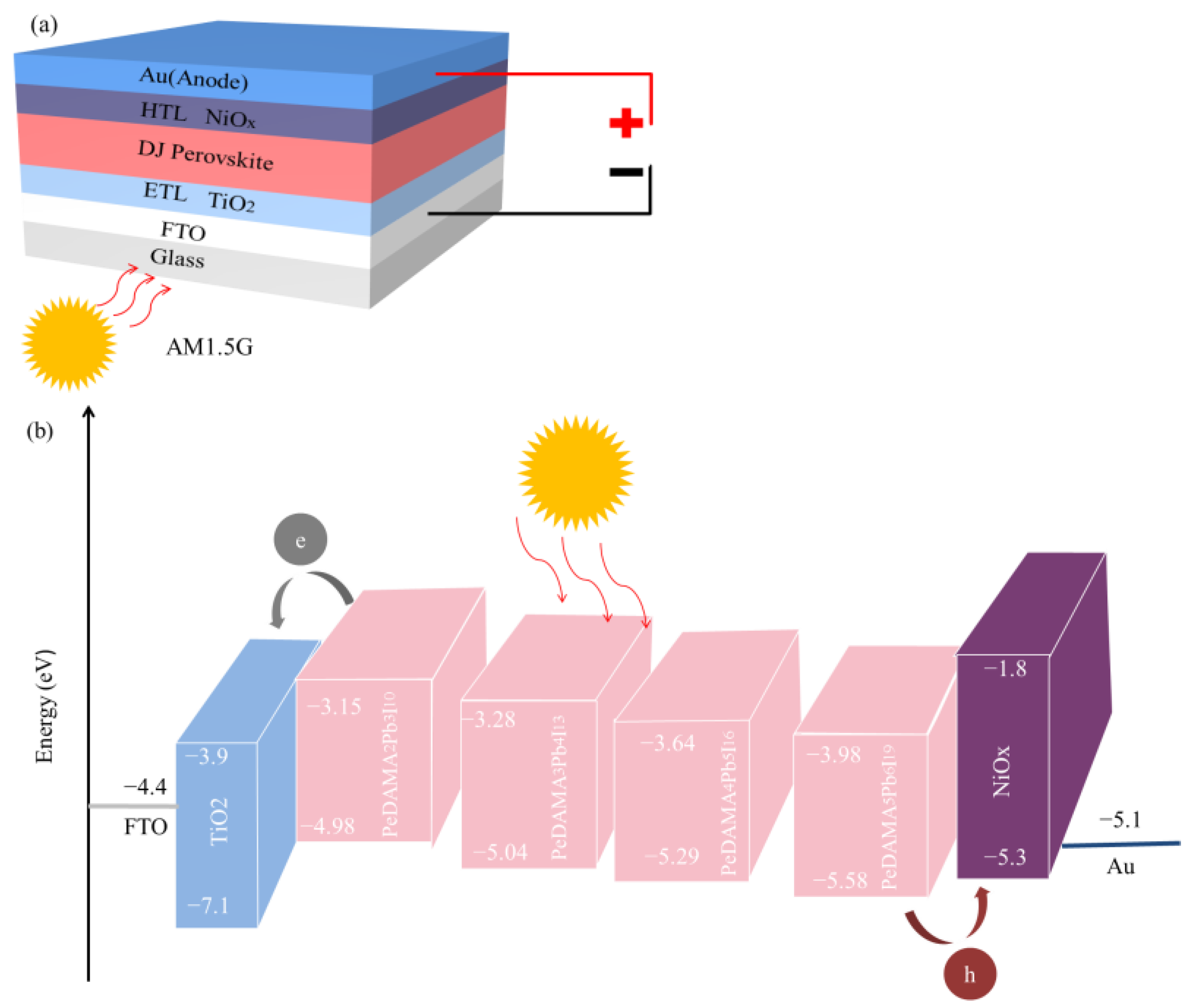
2.2. Model Structure and Material Parameters

Using SCAPS, we designed an N-I-P PSC with the structure glass/FTO/ETL/DJ perovskite/HTL/Au, as shown in Figure 1a. In this figure, TiO2 and NiOX were employed as the ETL and HTL, respectively. FTO served as the front contact, while Au acted as the metal back electrode. The DJ perovskite, encompassing PeDAMA2Pb3I10, PeDAMA3Pb4I13, PeDAMA4Pb5I16, and PeDAMA5Pb6I19, functioned as the active layer. Figure 1b depicts the energy levels of different materials. Excitons are generated when perovskite materials absorb photons with energies exceeding their bandgaps. Subsequently, the excitons migrate to the interface between the perovskite layers and the carrier transport layers, forming free electrons and free holes. These free electrons and free holes then traverse the ETL and HTL, respectively, and are ultimately collected by the corresponding electrodes.
The material parameter settings for constructing the initial models [14,18,25,26] and the interface parameters of the NiOx/DJ perovskite and DJ perovskite/TiO2 [19,27] were derived from authoritative studies to ensure the reliability of the simulation reference data sources. In Figure 2, J-V characteristic curves are presented for devices under the conditions of dark and light. Figure 2a–d correspond to PeDAMA2Pb3I10, PeDAMA3Pb4I13, PeDAMA4Pb5I16, and PeDAMA5Pb6I19, respectively. The diode rectification characteristics in all four initial models indicate the reliability of the structural design. Figure 3a demonstrates an improvement in the J-V characteristic curve when transitioning from PeDAMA2Pb3I10 to PeDAMA5Pb6I19. Figure 3b explains this phenomenon. Among the four types of perovskite materials, the bandgap order from large to small is PeDAMA2Pb3I10 > PeDAMA3Pb4I13 > PeDAMA4Pb5I16 > PeDAMA5Pb6I19. Consequently, the absorption of photons gradually improves from PeDAMA2Pb3I10 to PeDAMA5Pb6I19, indicating that PeDAMA5Pb6I19 and PeDAMA2Pb3I10 have the best and worst absorption of photons, respectively. Hence, PeDAMA5Pb6I19-based solar cells have the optimal quantum efficiency (QE), while PeDAMA2Pb3I10-based solar cells have the lowest QE. In general, all initial models exhibit good photon absorption below 780 nm, confirming their reliability. Therefore, the following section will explore the impact of the interface band offset between the ETL (TiO2) and the perovskite layer on the cell performance based on these models. Table 1 listed the basic parameters of the initial model while Table 2 displays key interface parameter settings.

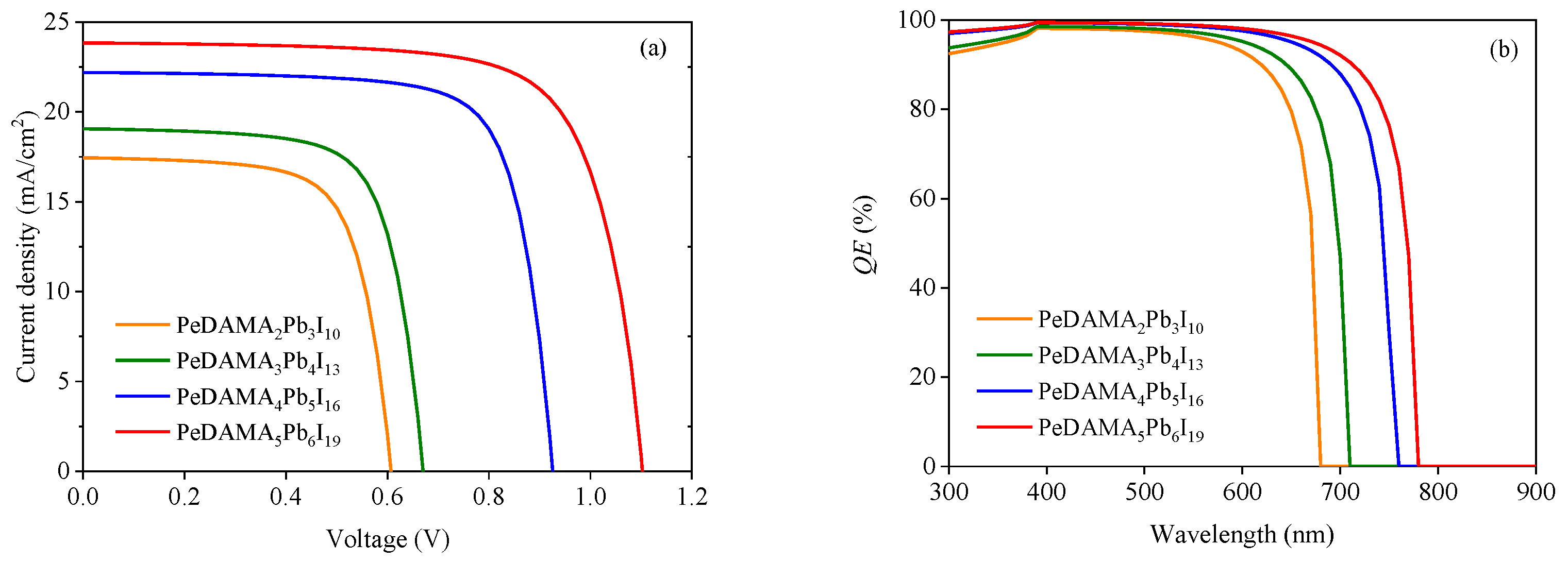
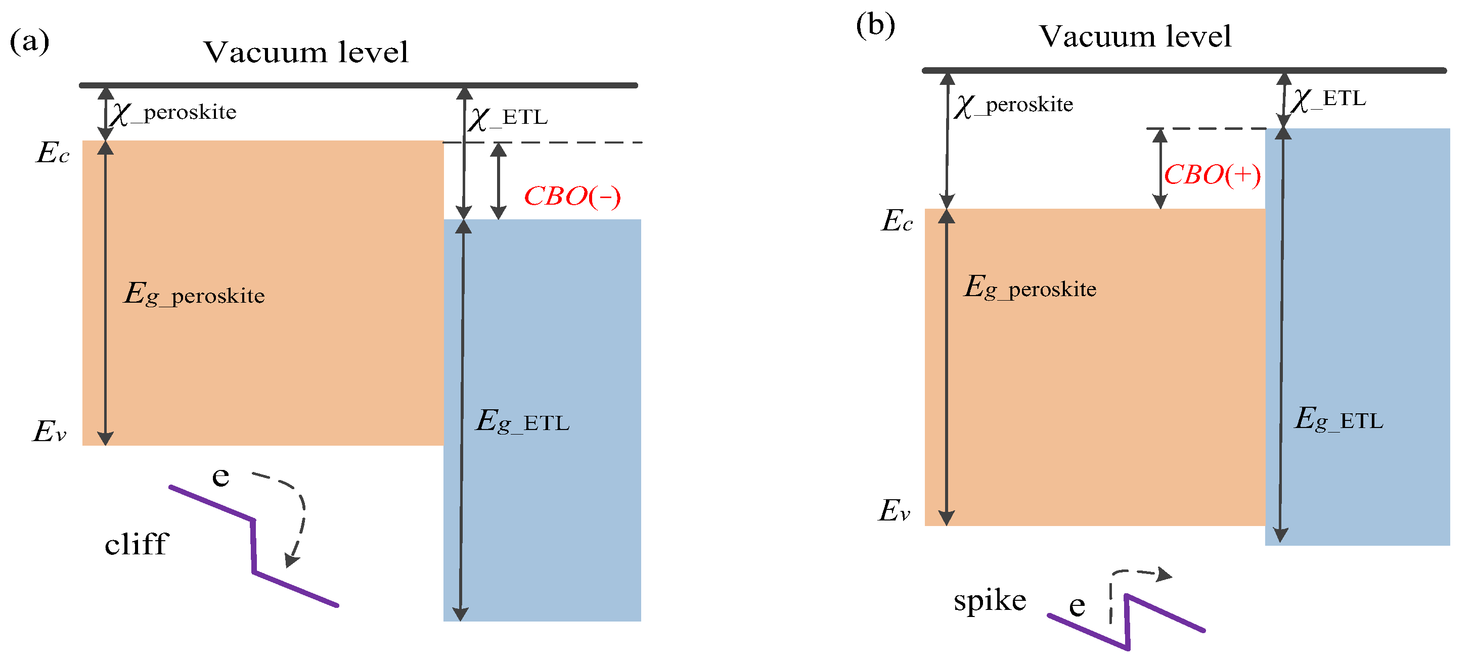
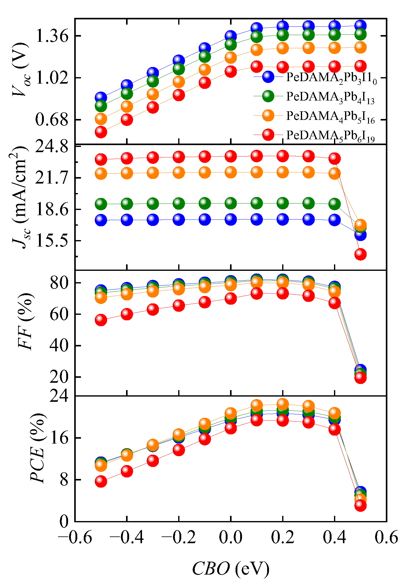
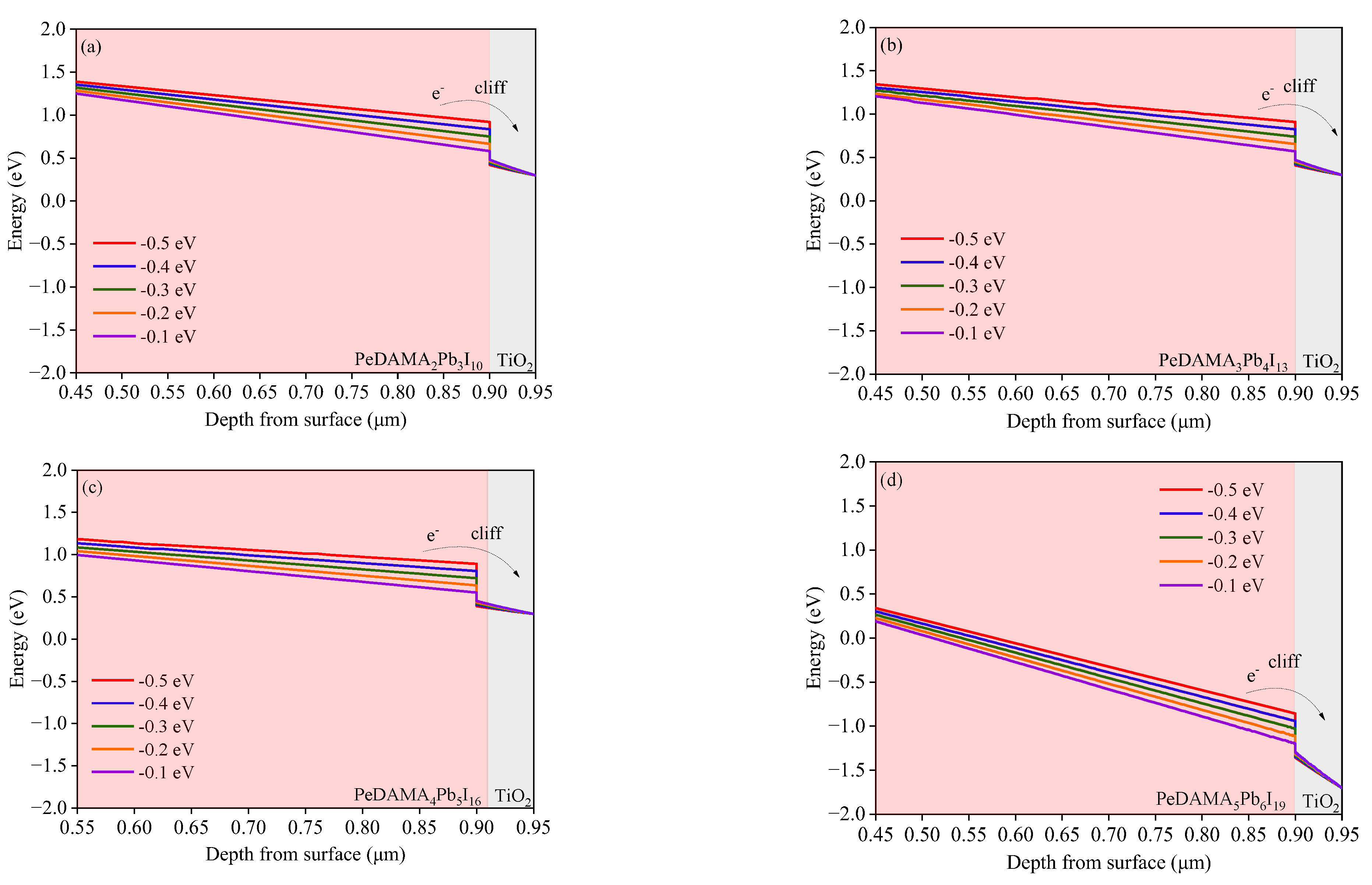
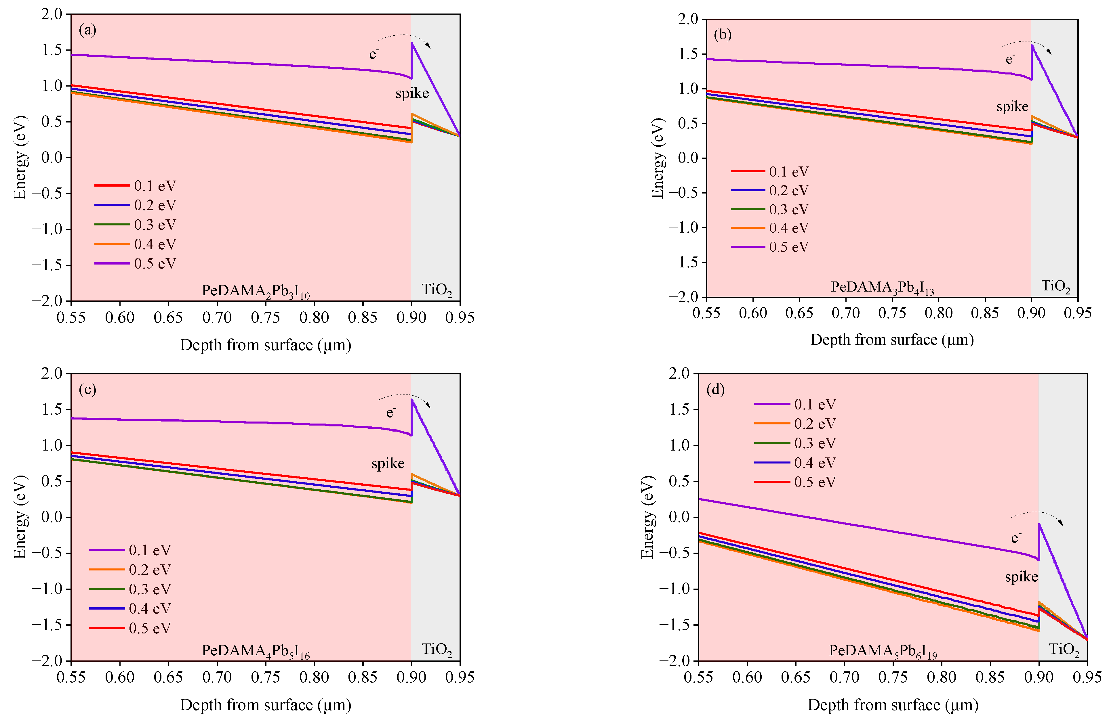
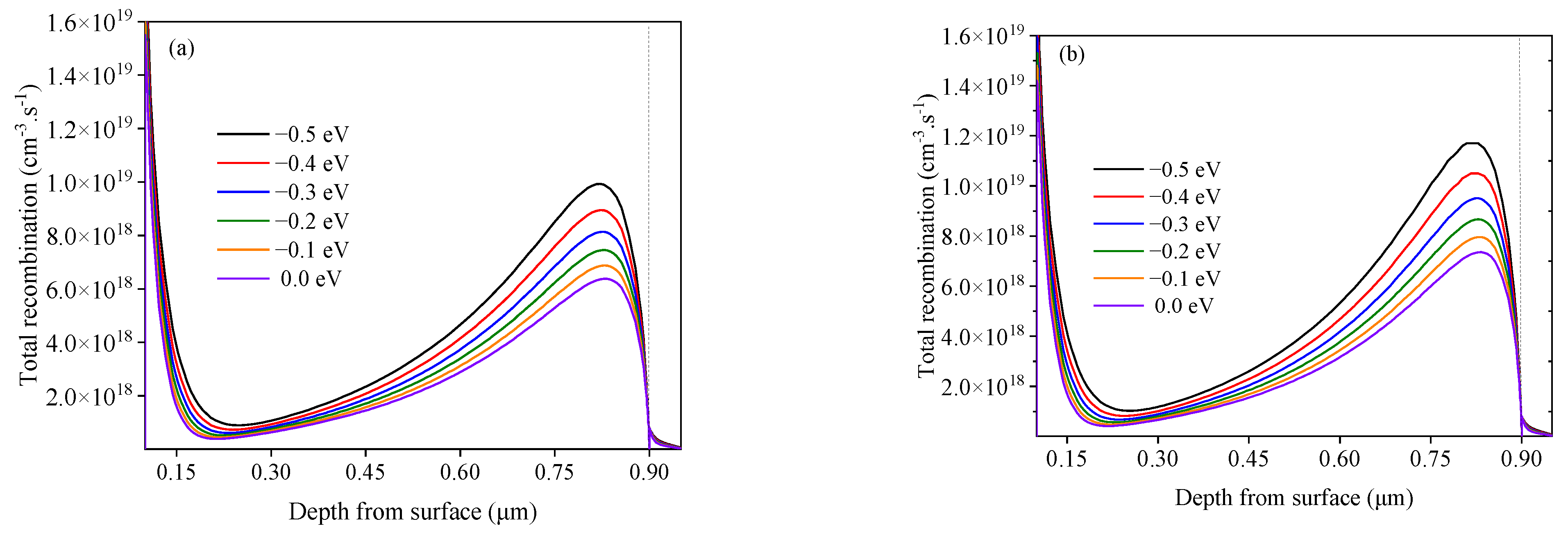
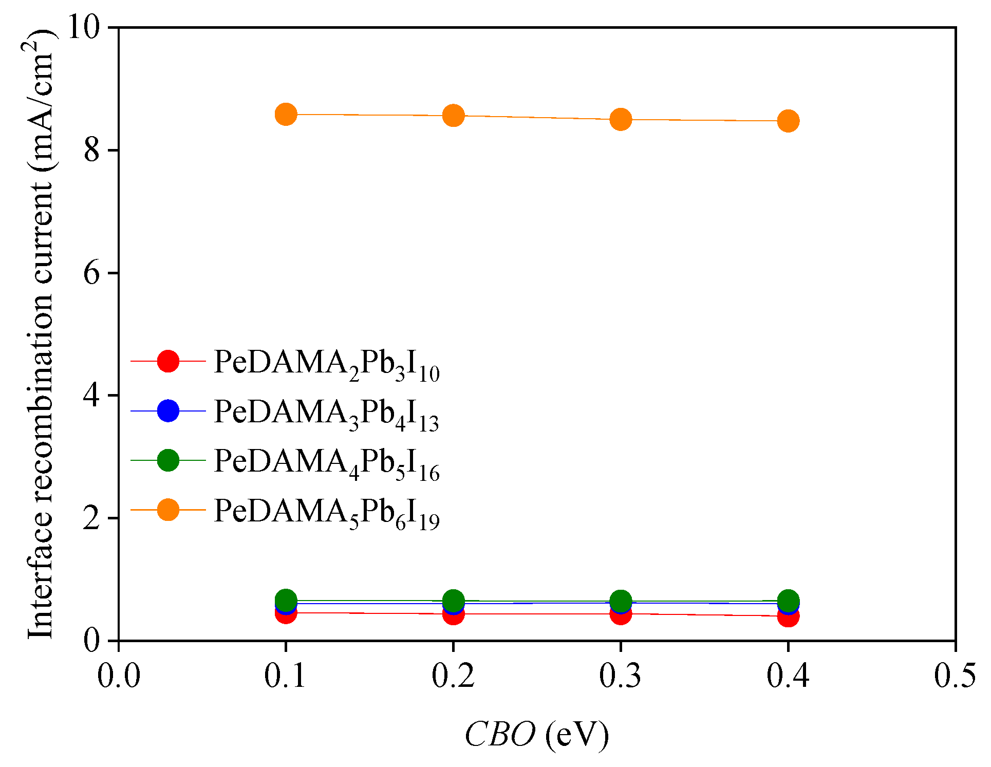
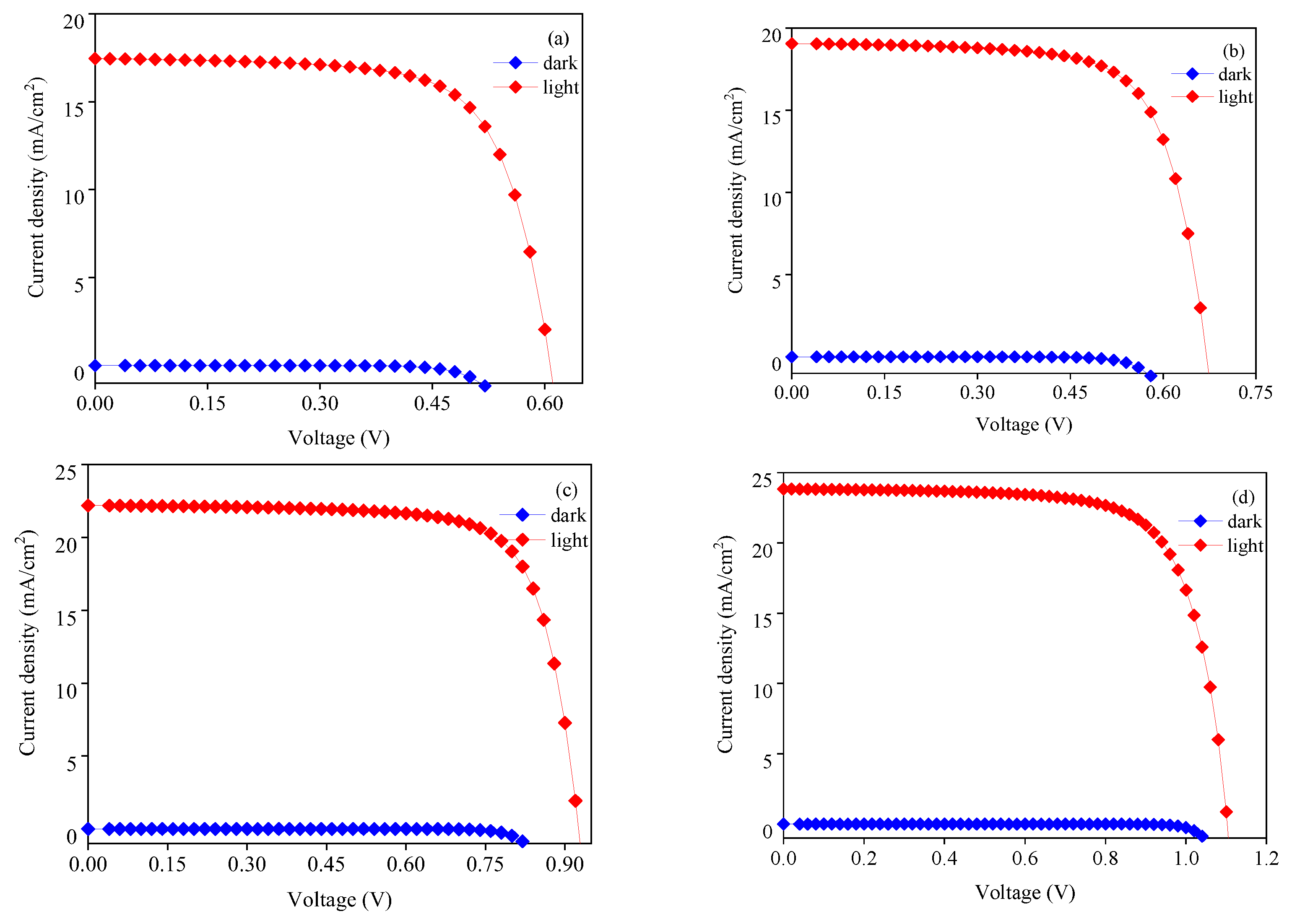
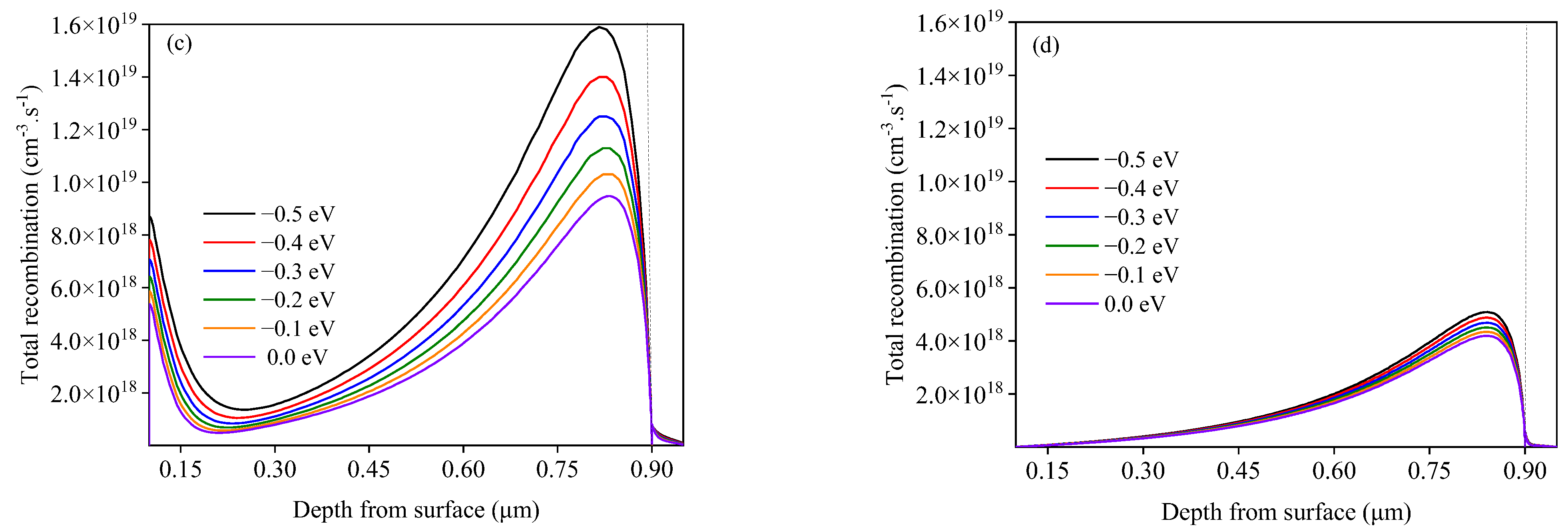
3. Results and Discussion

Figure 4 illustrates a schematic of the barrier structure at the interface between the perovskite layer and the ETL. The CBO, which stands for conduction band offset, quantifies the misalignment between the conduction band of the perovskite and the ETL. The CBO value is calculated by subtracting the conduction band level of the perovskite from that of the ETL. The magnitude of the CBO is closely related to the interface barrier. The CBO is negative when the conduction band level of the ETL is lower than that of the perovskite, and it is positive when the conduction band level of the ETL is higher. As depicted in Figure 4a, a negative CBO results in an energy cliff at the interface between the perovskite layer and the ETL. Conversely, in Figure 4b, a positive CBO leads to the formation of an energy spike at the same interface. The structural difference between a cliff and a spike is significant. An energy cliff does not impede the movement of photo-generated electrons, while an energy spike acts as an obstacle. Consequently, the energy required for a photo-generated electron to traverse these different barriers varies, leading to variations in the accumulation and interface recombination of carriers.
The CBO has a significant impact on interface recombination which is both theoretically supported [35,36,37] and experimentally demonstrated [38,39,40]. To analyze the relationship between the CBO and the performance of the DJ PSCs in this study, we maintained the CBO within the range of −0.5 to 0.5 eV. The simulation work adopted the control variable method. To control the value of the CBO, the electron affinity of the ETL was altered, while the other parameters of the materials listed in Table 1 remained unchanged. Figure 5 and Figure 6 display the simulation results. Figure 5 illustrates the trends in the cell output parameters (Voc, Jsc, FF, and PCE) with different CBO values, while the corresponding J-V characteristic curves are presented in Figure 6.
In Figure 5, when CBO values are negative, the Voc, FF, and PCE consistently increase from −0.5 eV to 0 eV, while the Jsc remains relatively unchanged. Conversely, positive CBO values in the range of 0.1–0.4 eV show less significant differences in output parameters which are larger than those observed in the negative range. However, with a further increase in the CBO, the cell performance rapidly declines. Similar trends are observed in Figure 6, in which J-V characteristic curves steadily increase as the CBO changes from −0.5 eV to 0 eV, almost overlapping and improving from 0.1–0.4 eV but exhibiting a severe S-shape when the CBO reaches 0.5 eV.
When the CBO is less than 0 eV, a cliff forms at the interface between the ETL and the perovskite. Conversely, when the CBO is positive, a spike forms, as depicted in Figure 7 and Figure 8, demonstrating a high degree of consistency between simulation results and theory. The activation energy for carrier recombination (Ea) assesses carrier recombination at the interface between the perovskite and the ETL. For positive CBO values, the Ea equals the band gap of the perovskite. In contrast, for a negative CBO, the Ea is defined by the difference between the band gap of the perovskite and the absolute value of the CBO. Consequently, negative CBO values increase the likelihood of interface recombination.
The formation of an energy cliff occurs as the CBO increases from −0.5 eV to 0 eV. This energy cliff, while not impending the movement of photo-generated electrons, results in a nearly unchanged Jsc. However, the activation energy Ea is smaller than the band gap of the perovskite, indicating that interface recombination predominantly influences the recombination mechanism [41,42,43]. Research has generally proven that Voc is closely tied to carrier recombination. Low carrier recombination has a positive effect on promoting Voc. The Ea measures the difficulty of carrier recombination. Carriers are more likely to recombine when the Ea is smaller. Therefore, it can be inferred that the Ea directly influences Voc. As the CBO gradually increases from −0.5 eV to 0 eV, the Ea also increases, leading to a gradual reduction in the likelihood of carrier recombination. Consequently, the Voc shows a continuous increase. Both Figure 9 and Figure 10 confirm that interface carrier recombination decreases gradually with an increase in the CBO from −0.5 eV to 0 eV. The decrease in carrier recombination signifies a reduction in the internal consumption of the device, contributing to a gradual increase in the FF. The concurrent increases in the Voc and FF further promote an overall rise in the PCE.
When the CBO ranges from 0.1 eV to 0.4 eV, an energy spike is formed. At this point, the Ea remains constant and is equal to the band gap of the perovskite, resulting in minimal differences in interface carrier recombination. Figure 11 illustrates that when the CBO is within this range, the fluctuation of the interface recombination current is weak, indicating insignificant changes in interface carrier recombination. Consequently, the Voc and FF almost remain unchanged. It has been demonstrated that a spike within this small range has a limited effect on the motion of photo-generated electrons [31]. As a result, Jsc experiences little change. The negligible variations in the Voc, Jsc, and FF translate to insignificant changes in the PCE. However, if the CBO further increases to 0.5 eV, it may induce a double-diode-like curvature, leading to a rapid decrease in the FF. Consequently, the PCE experiences a significant decrease.
The cells perform better when the CBO is in the range of 0.1–0.4 eV than when the CBO is negative. A positive CBO leads to the formation of an energy spike, which acts as a barrier and impedes the transport and collection of photo-generated electrons. However, research has shown that a spike within a small range has less effect on the motion of photo-generated electrons but a greater impact on the carrier recombination rate [31]. In other words, PSCs may achieve better performance when an energy spike forms at the interface between the perovskite and the ETL. Therefore, the Ea has a stronger impact when a spike is formed, and the cell performance improves when the CBO is positive and there is a spike within a small range. Figure 5 and Figure 6 demonstrate that controlling the CBO within 0.1–0.4 eV is beneficial for the better performance of DJ PSCs.

4. Conclusions

The effects of the CBOs of DJ PSCs were analyzed using the 1D solar cell simulator SCAPS. The CBO is negative when the ETL has a lower conduction band level than the DJ perovskite and vice versa. An energy cliff is formed at the interface between the DJ perovskite and ETL when the CBO is negative, and an energy spike is generated when the CBO is positive. When the CBO is negative and a cliff is formed, the movement of electrons is not suppressed, so Jsc remains almost unchanged. However, the Ea gradually increases with an increase in the CBO, reducing the interface carrier recombination, leading to continuous increases with increases in the Voc and FF. Thus, the PCE is improved. When the CBO is positive and a spike is generated, the Ea is equal to the band gap of the DJ perovskite, so the Voc and FF remain almost unchanged. It has been proven that the Ea has a more significant impact on cell performance when the CBO is relatively small, and simulation results indicate that when the CBO is 0.1–0.4 eV, the performances of DJ PSCs improve. These numerical simulation results should provide important guidelines for designing efficient DJ PSCs.

Author Contributions

Conceptualization, Y.G. and B.Q.; methodology, Y.G. and Z.Z.; software, C.Y. and G.Q.; validation, Y.G. and B.Q.; formal analysis, X.B.; investigation, Y.G. and C.Y.; data curation, X.B.; writing—original draft preparation, Y.G.; writing—review and editing, Y.L.; visualization, C.Y.; supervision, X.B. and Y.L. All authors have read and agreed to the published version of the manuscript.

Funding

This research was funded by the high-quality talents research startup fund from Yulin Normal University (G2019ZK24), a Guangxi Key Laboratory of optoelectronic information processing project (GD21101), a Guangxi University Young and Middle-aged Teachers’ Basic Scientific Research Ability Improvement Project (2022KY0580) and the Innovation and Entrepreneurship Training Program for College Students (202310606024, 202310606231).

Data Availability Statement

The data that support the findings of this study are available from the corresponding author upon reasonable request.

Acknowledgments

The authors are grateful to Marc Bergelman from the University of Gent for providing the SCAPS simulation program.

Conflicts of Interest

The authors declare no conflict of interest.

References

  1. Kojima, A.; Teshima, K.; Shirai, Y.; Miyasaka, T. Organometal Halide Perovskites as Visible-Light Sensitizers for Photovoltaic Cells. J. Am. Chem. Soc. 2009, 131, 6050–6051. [Google Scholar] [CrossRef]
  2. Park, J.; Kim, J.; Yun, H.S.; Paik, M.J.; Noh, E.; Mun, H.J.; Kim, M.G.; Shin, T.J.; Seok, S.I. Controlled Growth of Perovskite Layers with Volatile Alkylammonium Chlorides. Nature 2023, 616, 724–730. [Google Scholar] [CrossRef] [PubMed]
  3. Gan, Y.-J.; Bi, X.-G.; Liu, Y.-C.; Qin, B.-Y.; Li, Q.-L.; Jiang, Q.-B.; Mo, P. Numerical Investigation Energy Conversion Performance of Tin-Based Perovskite Solar Cells using Cell Capacitance Simulator. Energies 2020, 13, 5907. [Google Scholar] [CrossRef]
  4. Gan, Y.-J.; Zhao, D.; Qin, B.-Y.; Bi, X.-G.; Liu, Y.-C.; Ning, W.-L.; Yang, R.-Z.; Jiang, Q.-B. Numerical Simulation of High-Performance CsPbI3/FAPbI3 Heterojunction Perovskite Solar Cells. Energies 2022, 15, 7301. [Google Scholar] [CrossRef]
  5. Shao, M.; Bie, T.; Yang, L.; Gao, Y.; Jin, X.; He, F.; Zheng, N.; Yu, Y.; Zhang, X. Over 21% Efficiency Stable 2D Perovskite Solar Cells. Adv. Mater. 2022, 34, 2107211. [Google Scholar] [CrossRef] [PubMed]
  6. Chen, J.; Wang, B.; Huang, G.; Cheng, Q.; Li, Y.; Li, X.; Li, S.; Li, K.; Zhu, L.; Zhai, Z.; et al. Thermally Regulated Energy Loss in Dion-Jacobson Perovskite Solar Cells. Sol. RRL 2022, 6, 2200636. [Google Scholar] [CrossRef]
  7. Huang, G.; Chen, J.; Wang, B.; Cheng, Q.; Li, Y.; Zafar, S.U.; Yue, T.; Yan, Y.; Du, W.; Zhang, H.; et al. Solvent Effect on Film Formation and Trap States of Two Dimensional Dion-Jacobson Perovskite. Nano Lett. 2022, 22, 7545–7553. [Google Scholar] [CrossRef]
  8. Mao, L.; Ke, W.; Pedesseau, L.; Wu, Y.; Katan, C.; Even, J.; Wasielewski, M.R.; Stoumpos, C.C.; Kanatzidis, M.G. Hybrid DionJacobson 2D Lead Iodide Perovskites. J. Am. Chem. Soc. 2018, 140, 3775–3783. [Google Scholar] [CrossRef]
  9. Stoumpos, C.C.; Cao, D.H.; Clark, D.J.; Young, J.; Rondinelli, J.M.; Jang, J.I.; Hupp, J.T.; Kanatzidis, M.G. Ruddlesden–Popper hybrid lead iodide perovskite 2Dhomologous semiconductors. Chem. Mater. 2016, 28, 2852–2867. [Google Scholar] [CrossRef]
  10. Dong, Y.; Dong, X.; Lu, D.; Chen, M.; Zheng, N.; Wang, R.; Li, Q.; Xie, Z.; Liu, Y. Orbitalinteractions between the organic semiconductor spacer and the inorganic layer in dion-jacobson perovskites enable efficient solar cells. Adv. Mater. 2023, 35, 2205258. [Google Scholar] [CrossRef]
  11. Mohammed, M.K.; Al-Mousoi, A.K.; Kumar, A.; Sabugaa, M.M.; Seemaladinne, R.; Pandey, R.; Al-Kahtani, A.A. Harnessing the potential of Dion-Jacobson perovskite solar cells: Insights from SCAPS simulation techniques. J. Alloys Compd. 2023, 963, 171246. [Google Scholar] [CrossRef]
  12. Xiang, J.; Li, X.; Gong, S.; Wang, S.; Chen, X.; Zhang, F. Green Antisolvent-Induced Homogeneous Phase Distribution for Efficient and Stable MA-Free 2D Perovskite Solar Cells. Chem. Eng. J. 2023, 460, 141758. [Google Scholar] [CrossRef]
  13. Chen, Y.; Hu, J.; Xu, Z.; Jiang, Z.; Chen, S.; Xu, B.; Xiao, X.; Liu, X.; Forberich, K.; Brabec, C.J.; et al. Managing Phase Orientation and Crystallinity of Printed Dion-Jacobson 2D Perovskite Layers via Controlling Crystallization Kinetics. Adv. Funct. Mater. 2022, 32, 2112146. [Google Scholar] [CrossRef]
  14. Wu, H.; Lian, X.; Tian, S.; Zhang, Y.; Qin, M.; Zhang, Y.; Wang, F.; Lu, X.; Wu, G.; Chen, H. Additive-Assisted Hot-Casting Free Fabrication of Dion-Jacobson 2D Perovskite Solar Cell with Efficiency Beyond 16%. Sol. RRL 2020, 4, 2070074. [Google Scholar] [CrossRef]
  15. Zhang, X.; Yang, T.; Ren, X.; Zhang, L.; Zhao, K.; Liu, S. Film Formation Control for High Performance Dion-Jacobson 2D Perovskite Solar Cells. Adv. Energy Mater. 2021, 11, 2002733. [Google Scholar] [CrossRef]
  16. Zheng, Y.; Niu, T.; Qiu, J.; Chao, L.; Li, B.; Yang, Y.; Li, Q.; Lin, C.; Gao, X.; Zhang, C. Oriented and uniform distribution of Dion–Jacobson phase perovskites controlled by quantum well barrier thickness. Sol. Rrl 2019, 3, 1900090. [Google Scholar] [CrossRef]
  17. Su, P.; Bai, L.; Bi, H.; Liu, B.; Chen, S.; Lee, D.; Yang, H.; Chen, C.; Zang, Z.; Chen, J. Interfacial Gradient Energy Band Alignment Modulation via Ion Exchange Reaction toward Efficient and Stable Methylammonium-Free Dion-Jacobson Quasi-2D Perovskite Solar Cells. J. Power Sources 2021, 506, 230213. [Google Scholar] [CrossRef]
  18. Wu, H.; Lian, X.; Li, J.; Zhang, Y.; Zhou, G.; Wen, X.; Xie, Z.; Zhu, H.; Wu, G.; Chen, H. Merged Interface Construction toward Ultra-Low Voc Loss in Inverted Two-Dimensional Dion-Jacobson Perovskite Solar Cells with Efficiency over 18. J. Mater. Chem. A 2021, 9, 12566–12573. [Google Scholar] [CrossRef]
  19. Jin, L.; Ren, N.; Wang, P.; Li, R.; Xue, Q.; Huang, F.; Zhang, X.; Zhao, Y.; Zhang, X. Secondary Anti-Solvent Treatment for Efficient 2D Dion-Jacobson Perovskite Solar Cells. Small 2023, 19, 2205088. [Google Scholar] [CrossRef]
  20. Zhai, Z.; Chen, J.; Liu, Q.; Jiang, S.; Li, Y. Defect Regulation of Efficient Dion–Jacobson Quasi-2D Perovskite Solar Cells via a Polyaspartic Acid Interlayer. ACS Appl. Mater. Interfaces 2023, 15, 38068–38079. [Google Scholar] [CrossRef]
  21. Burgelman, M.; Nollet, P.; Degrave, S. Modelling polycrystalline semiconductor solar cells. Thin Solid films 2000, 361, 527–532. [Google Scholar] [CrossRef]
  22. Lee, K.M.; Lin, W.J.; Chen, S.H.; Wu, M.C. Control of TiO2 electron transport layer properties to enhance perovskite photovoltaics performance and stability. Org. Electron. 2020, 77, 105406. [Google Scholar] [CrossRef]
  23. Wu, M.C.; Chan, S.H.; Lee, K.M.; Chen, S.H.; Jao, M.H.; Chen, Y.F.; Su, W.F. Enhancing the efficiency of perovskite solar cells using mesoscopic zinc-doped TiO2 as the electron extraction layer through band alignment. J. Mater. Chem. A 2018, 6, 16920–16931. [Google Scholar] [CrossRef]
  24. Mohamad Noh, M.F.; Teh, C.H.; Daik, R.; Lim, E.L.; Yap, C.C.; Ibrahim, M.A.; Ahmad Ludin, N.; Bin Mohd Yusoff, A.R.; Jang, J.; Mat Teridi, M.A. The architecture of the electron transport layer for a perovskite solar cell. J. Mater. Chem. C 2018, 6, 682–712. [Google Scholar] [CrossRef]
  25. Zhou, H.; Chen, Q.; Li, G.; Luo, S.; Song, T.b.; Duan, H.S.; Hong, Z.; You, J.; Liu, Y.; Yang, Y. Interface engineering of highly efficient perovskite solar cells. Science 2014, 345, 542–546. [Google Scholar] [CrossRef]
  26. Cha, M.; Da, P.; Wang, J.; Wang, W.; Chen, Z.; Xiu, F.; Zheng, G.; Wang, Z.S. Enhancing Perovskite Solar Cell Performance by Interface Engineering Using CH3NH3PbBr0.9I2.1 Quantum Dots. J. Am. Chem. Soc. 2016, 138, 8581–8587. [Google Scholar] [CrossRef] [PubMed]
  27. Du, H.J.; Wang, W.C.; Ma, B.; Long, T.; Zhu, J.Z. Band Structure Adjustment of Solar Cells by Gradient Doping. Mat. Sci. Semicon. Proc. 2015, 40, 570–577. [Google Scholar] [CrossRef]
  28. Li, N.; Yan, J.; Ai, Y.; Jiang, E.; Lin, L.; Shou, C.; Yan, B.; Sheng, J.; Ye, J. A low-temperature tio2 /sno2 electron transport layer for high-performance planar perovskite solar cells. Sci. China Mater. 2020, 63, 207–215. [Google Scholar] [CrossRef]
  29. Du, H.J.; Wang, W.C.; Zhu, J.Z. Device Simulation of Lead-Free CH3NH3SnI3 Perovskite Solar Cells with High Efficiency. Chin. Phys. B 2016, 25, 108802. [Google Scholar] [CrossRef]
  30. Al-Mousoi, A.K.; Mohammed, M.K.; Pandey, R.; Madan, J.; Dastan, D.; Ravi, G.; Sakthivel, P. Simulation and analysis of lead-free perovskite solar cells incorporating cerium oxide as electron transporting layer. RSC Adv. 2022, 12, 32365–32373. [Google Scholar] [CrossRef]
  31. Hossain, M.K.; Arnab, A.; Das, R.C.; Hossain, K.; Rubel, M.; Rahman, M.F.; Bencherif, H.; Emetere, M.; Mohammed, M.K.; Pandey, R. Combined DFT, SCAPS-1D, and wxAMPS frameworks for design optimization of efficient Cs2BiAgI6-based perovskite solar cells with different charge transport layers. RSC Adv. 2022, 12, 35002–35025. [Google Scholar] [CrossRef]
  32. Gan, Y.-J.; Qiu, G.-X.; Qin, B.-Y.; Bi, X.-G.; Liu, Y.-C.; Nie, G.-C.; Ning, W.-L.; Yang, R.-Z. Numerical Analysis of Stable (FAPbI3)0.85(MAPbBr3)0.15-Based Perovskite Solar Cell with TiO2/ZnO Double Electron Layer. Nanomaterials 2023, 13, 1313. [Google Scholar] [CrossRef]
  33. Lakhdar, N.; Hima, A. Electron transport material effect on performance of perovskite solar cells based on CH3NH3GeI3. Opt. Mater. 2020, 99, 109517. [Google Scholar] [CrossRef]
  34. Huang, H.-C.; Yuan, E.-H.; Zhang, D.-S.; Sun, D.-X.; Yang, M.-H.; Zheng, Z.-Y.; Zhang, Z.-L.; Gao, L.; Panezai, S.; Qiu, K.-F. Free field of view infrared digital holography for mineral crystallization. Cryst. Growth Des. 2023, 23, 7992–8008. [Google Scholar] [CrossRef]
  35. Klenk, R. Characterization and modeling of chalcopyrite solar cells. Thin Solid Films 2001, 387, 135–140. [Google Scholar] [CrossRef]
  36. Minemoto, T.; Matsui, T.; Takakura, H.; Hamakawa, Y.; Negami, T.; Hashimoto, Y.; Uenoyama, T.; Kitagawa, M. Theoretical analysis of the effect of conduction band offset of window/CIS layers on performance of CIS solar cells using device simulation. Sol. Energy Mater. Sol. Cell 2001, 67, 83–88. [Google Scholar] [CrossRef]
  37. Gloeckler, M.; Sites, J. Efficiency limitations for wide-band-gap chalcopyrite solar cells. Thin Solid Films 2005, 480, 241–245. [Google Scholar] [CrossRef]
  38. Minemoto, T.; Hashimoto, Y.; Satoh, T.; Negami, T.; Takakura, H.; Hamakawa, Y. Cu(In,Ga)Se2 solar cells with controlled conduction band offset of window/Cu(In,Ga)Se2 layers. J. Appl. Phys. 2001, 89, 8327–8330. [Google Scholar] [CrossRef]
  39. Minemoto, T.; Hashimoto, Y.; Satoh, T.; Kolahi, W.S.; Negami, T.; Takakura, H.; Hamakawa, Y. Control in conduction band offset in wide-gap Cu(In,Ga)Se2 solar cells. Sol. Energy Mater. Sol. Cell 2003, 75, 121–126. [Google Scholar] [CrossRef]
  40. Torndahl, T.; Platzer-Bjorkman, C.; Kessler, J.; Edoff, M. Atomic layer deposition of Zn1−xMgxO buffer layers for Cu(In,Ga)Se2 solar cells. Prog. Appl. 2007, 15, 225–235. [Google Scholar] [CrossRef]
  41. Turcu, M.; Rau, U. Fermi level pinning at CdS/Cu(In,Ga)(Se,S)2 interfaces: Effect of chalcopyrite alloy composition. J. Phys. Chem. Solids 2003, 64, 1591–1595. [Google Scholar] [CrossRef]
  42. Tanaka, K.; Minemoto, T.; Takakura, H. Analysis of heterointerface recombina-tion by Zn1−xMgxO for window layer of Cu(In,Ga)Se2 solar cells. Sol. Energy 2009, 83, 477–479. [Google Scholar] [CrossRef]
  43. Minemoto, T.; Murata, M. Theoretical analysis on effect of band offsets in perovskite solar cells. Sol. Energy Mater. Sol. Cells 2015, 133, 8–14. [Google Scholar] [CrossRef]
Figure 1. Initial model and its energy band structure: (a) initial model structure; (b) energy band structure diagram.
Energies 16 07889 g001
Figure 2. J-V characteristic curves of the initial models under different illumination conditions: (a) PeDAMA2Pb3I10-based model; (b) PeDAMA3Pb4I13-based model; (c) PeDAMA4Pb5I16-based model; (d) PeDAMA5Pb6I19-based model.
Energies 16 07889 g002
Figure 3. J-V characteristic curves and quantum efficiency curves of the initial models: (a) J-V characteristic curves; (b) quantum efficiency curves.
Energies 16 07889 g003
Figure 4. Schematic of the barrier structure at the interface between perovskite and ETL: (a) CBO is negative; (b) CBO is positive.
Energies 16 07889 g004
Figure 5. Trends in the cell output parameters with a change in the CBO.
Energies 16 07889 g005
Figure 6. J-V characteristic curves under different CBOs for different models: (a) PeDAMA2Pb3I10-based model; (b) PeDAMA3Pb4I13-based model; (c) PeDAMA4Pb5I16-based model; (d) PeDAMA5Pb6I19-based model.
Energies 16 07889 g006
Figure 7. Interface band structures of DJ PSCs with negative CBOs: (a) PeDAMA2Pb3I10, (b) PeDAMA3Pb4I13, (c) PeDAMA4Pb5I16, and (d) PeDAMA5Pb6I19.
Energies 16 07889 g007
Figure 8. Interface band structures of DJ PSCs with positive CBOs: (a) PeDAMA2Pb3I10, (b) PeDAMA3Pb4I13, (c) PeDAMA4Pb5I16, and (d) PeDAMA5Pb6I19.
Energies 16 07889 g008
Figure 9. Interface recombination current at the perovskite/ETL interface when the CBO is negative.
Energies 16 07889 g009
Figure 10. Total recombination at the perovskite/ETL interface when the CBO is negative. (a) PeDAMA2Pb3I10, (b) PeDAMA3Pb4I13, (c) PeDAMA4Pb5I16, and (d) PeDAMA5Pb6I19.
Energies 16 07889 g010aEnergies 16 07889 g010b
Figure 11. Interface recombination current at the perovskite/ETL interface with a positive CBO.
Energies 16 07889 g011
Table 1. Basic parameters of the initial model.
ParameterNiOxPeDAMA2Pb3I10PeDAMA3Pb4I13PeDAMA4Pb5I16PeDAMA5Pb6I19TiO2
Thickness/nm10080080080080050
Band gap/eV3.51.831.761.651.63.2
Electron affinity/eV1.83.153.283.643.983.9
Dielectric permittivity10.7252525259
Electron mobility/cm2/V.s121.41.41.41.420
Hole mobility/cm2/V.s2.80.30.30.30.310
Acceptor concentration/cm−33.0 × 101800000
Donor concentration/cm−3000001.0 × 10−16
CB effective density of states/cm−32.8 × 10197.5 × 10177.5 × 10177.5 × 10177.5 × 10171.0 × 1021
VB effective density of states/cm−31.0 × 10181.8 × 10181.8 × 10181.8 × 10181.8 × 10182.0 × 1020
Defect typeNeutralNeutralNeutralNeutralNeutralNeutral
Capture cross-section for electrons/cm21.0 × 10−151.0 × 10−151.0 × 10−151.0 × 10−151.0 × 10−151.0 × 10⁻¹⁵
Capture cross-section for holes/cm21.0 × 10−151.0 × 10−151.0 × 10−151.0 × 10−151.0 × 10−151.0 × 10⁻¹⁵
Total defect density/cm−31.0 × 10−152.5 × 10−142.5 × 10−142.5 × 10−142.5 × 10−141.0 × 10⁻¹⁶
Table 2. Interface parameter settings.
ParameterNiOx/DJ PerovskiteDJ Perovskite/TiO2
Type of DefectNeutralNeutral
Cross-Section for Electron Capture/cm21.0 × 10−151.0 × 10⁻¹⁵
Cross-Section for Hole Capture/cm21.0 × 10−151.0 × 10⁻¹⁵
Distribution of Energiessinglesingle
Reference for Energy Level of DefectAbove the highest EvAbove the highest Ev
Energy with Respect to Reference/eV0.6 0.6
Total Density of Defects/cm−31.0 × 10101.0 × 1010
Disclaimer/Publisher’s Note: The statements, opinions and data contained in all publications are solely those of the individual author(s) and contributor(s) and not of MDPI and/or the editor(s). MDPI and/or the editor(s) disclaim responsibility for any injury to people or property resulting from any ideas, methods, instructions or products referred to in the content.

