Article

Double-Coupling Resonant Network for Dynamic IPT Systems Used in EV Charging Applications

by
Valter S. Costa
1,2,
André M. S. Mendes
1,2,
Emanuel Marques
1,2 and
Marina S. Perdigão
2,3,*
1
Department of Electrical and Computer Engineering (DEEC), University of Coimbra, Pole 2, P-3030-290 Coimbra, Portugal
2
Instituto de Telecomunicações, University of Coimbra, Pole 2, P-3030-290 Coimbra, Portugal
3
Polytechnic Institute of Coimbra, IPC-ISEC, DEE, P-3045-093 Coimbra, Portugal
*
Author to whom correspondence should be addressed.
Energies 2023, 16(21), 7269; https://doi.org/10.3390/en16217269
Submission received: 5 August 2023 / Revised: 12 September 2023 / Accepted: 13 October 2023 / Published: 26 October 2023
(This article belongs to the Special Issue Wireless Charging System for Electric Vehicles)

Abstract

:
Dynamic inductive power transfer (DIPT) systems as well as static inductive power transfer (SIPT) systems are typically implemented with H-bridge inverters with resonant compensation networks to control and limit the charging current. However, contrary to SIPT, DIPT implies inherent displacements, in the travel direction, as well as the already expected misalignments (vertical and lateral). The challenges imposed by this feature have an impact on the selected compensation network. Typical single-coupling resonant topologies SS, SP, PS, PP, LCL-S and LCL-P are considered. In this work, a double-coupling SSS topology is proposed for DIPT applications to overcome the limitations of classical topologies. A resonant converter topology with natural current and voltage limitation under misalignment conditions is preferable. This paper performs a finite element analysis (FEA) simulation of the magnetic coupler (MC) in order to extract the coupling factor and self and mutual inductances as a function of the electric vehicle (EV) movement. The MC parameters are used to build a model in MATLAB/Simulink with coupling variation in order to assess the converter behavior under misalignment conditions. The simulation and experimental results demonstrate the applicability of the double-coupling SSS topology for DIPT application by exhibiting safe converter operation under the full range of coupling and load operation (full to no-coupling and full to no-load).

1. Introduction

The current growth of electric vehicles (EVs) on the road leads in particular to the need for batteries to store the required electricity to power the EV. Different battery technologies are used in EV applications. Table 1 summarizes some of the main characteristics of different battery technologies [1]. It is possible to see that Lithium (Li)-based technologies are preferred nowadays for EV applications since they present the highest energy density and power density, which is desired to achieve higher EV autonomy with lower weight and have a relatively high efficiency and number of life cycles, increasing battery life.
One way to charge the batteries is using wireless power transfer (WPT) systems, in particular inductive power transfer (IPT) systems. Several WPT/IPT companies and research groups have been studying and developing different WPT systems for static and/or dynamic applications and for different power levels, from regular EVs to higher power buses. Table 2 lists some research groups and companies working in IPT solutions for EVs. Witricity is an MIT-based company composed by scientists that demonstrated nonradiative energy transfer back in 2007. Witricity acquired Qualcomm Halo, a spin-off company from Auckland University that holds the majority of intellectual property of IPT technology. The ENRX group has solutions for heavy-duty vehicles in both static and dynamic conditions up to 180 kW. WAVE by Ideanomics ensures an up time above 95% in transportation buses with their 250 kW IPT systems. The Swiss-based Brusa company offers a 11 kW static charger, whereas Wiferion was recently acquired by Tesla to incorporate IPT technology into their fleet. Therefore, it is clear that IPT is considered a hot topic of research, and it has several challenges to overcome. These include maximum power transfer and power transfer capability, tolerance to misalignments, power ratings, and the respective resonant compensation network required. Hence, in particular, dynamic IPT systems are a hot research topic.
IPT can be divided into static (SIPT) and dynamic (DIPT), whether the electric vehicle (EV) is static or in motion during the charging process [2]. The main goal in SIPT is to achieve maximum power transfer for a specific range of load variation ( R o = V o / I o ), considering constant coupling, i.e., ability to fully charge the battery (from State of Charge S o C = S o C m i n S o C m a x ) in constant current (CC) mode or constant voltage (CV) mode. The ideal power transfer conditions are found with a perfect alignment between the transmitter and the receiver at nominal current (at maximum coupling). Even if small misalignments are considered, the power transfer can be relatively high [3]. Conversely, DIPT allows charging the EV in motion, decreasing the stop-charging time, eliminating the range anxiety associated to EVs, and also avoiding queuing at charging stations.
Typically in IPT systems, the maximum power transfer is achieved at perfect alignment, which means that transmitter and receiver pads are perfectly aligned. If there is a misalignment between the pads, perhaps due to the way the EV is parked relative to the transmitter pad, the coupling factor decreases, which implies lower power transfer capability. In SIPT, it is considered that, once the EV is parked, it does not move, so the misalignment, if it exists, remains constant during the charging process, affecting the power transfer capability and thus the charging time. Considering this constant misalignment, it is possible in SIPT applications to implement misalignment compensation techniques, even before the charging process starts, to minimize the misalignment effect [4]. Contrary to static operation, in dynamic IPT operation, inherent displacements occur due to the EV movement in the travel direction. This means constant variation of the coupling factor as the EV moves above each transmitter pad. Adding to this, also lateral and vertical misalignments are expected depending on the driver’s ability to drive following the charging lane, as well as the road conditions such as bumps and holes along the road. This means that the inherent movement in DIPT affects the power transfer capability even if the perfect trajectory of the charging lane is followed. If the EV deviates from this trajectory, for example, laterally, the coupling factor decreases, reducing the power transfer to the EV.
DIPT systems can be classified according to the transmitter pad configuration into distributed or lumped magnetic structures [5,6]. Distributed magnetic structures include elongated tracks that ensure a continuous power transfer with a constant coupling factor. The large inductance of the track, however, reduces the overall coupling factor and requires higher voltage levels to drive the necessary transmitter current. Additionally, compliance with the ICNIRP guidelines on human exposure leakage magnetic field levels is only achieved at wider distances [2]. Lumped DIPT systems, on the other hand, consist of multiple discrete segmented transmitter pads placed along the roadway where the power transfer to the vehicle occurs. The size and geometry of these transmitter pads are similar to SIPT systems. However, given the continuous movement of the vehicle, the coupling factor varies between a null and maximum value, and load levels can have similar patterns (no-load and full-load).
While SIPT systems are extensively analyzed in the literature with already available commercial solutions, DIPT systems still present challenges related to the vehicle’s movement. The MC coupling factor as well as load value are changing, and consequently, the impedance at source terminals is also changing. Therefore, a converter topology and compensation network should be selected in order to keep primary-side current and voltages values manageable, not exceeding maximum specified ratings. Although some literature refer briefly the acceptable solutions [7,8,9,10,11,12], there is still room for the analysis and optimization of the feeding system in terms of compensation topologies for DIPT.
Figure 1a presents the transmitter placed on the roadway, represented in red and green, and the receiver onboard the EV, represented in blue and purple. The gray rectangles represent the ferrite cores in the receiver pad, used to improve the MC coupling factor. Figure 1b depicts the mutual inductance M T x R x evolution as a function of vehicle movement and the point at which it achieves its maximum value, corresponding to the point of maximum achievable coupling and a perfect alignment between the EV receiver and transmitter pad. Additionally, this figure presents the side view of the MC pads in the perfect alignment position and the off-board power supply. The y axis depicts the EV movement in the travel direction. The x axis refers to lateral misalignments relative to the trajectory of movement, and the z axis represents vertical misalignments, which are commonly referred to as airgap, if the height of the EV varies due to bumps or holes in the roadway, for example. Both these misalignments can affect the power transfer. As the EV moves, the mutual inductance presents a characteristic bell-shaped blue curve as in Figure 1b.
Natural EV displacement in DIPT implies considering the full range of bell-shaped characteristic curves, typically obtained for mutual inductances or coupling factors M T x R x and k T x R x (where k T x R x = M T x R x L T x L R x ) , respectively [13]. Due to the inherent EV movement, coupling variations k T x R x are expected, where T x and R x refer to transmitter and receiver pads, respectively. Coupling factor k T x R x is always proportional to the value of the mutual inductance M T x R x . Thus, random SoC levels may affect the converter power transfer, and so will the inherent coupling variations.
IPT systems use resonant converters to improve power transfer capability with Series (S) or Parallel (P) compensations, for example, which can be used in either the transmitter or receiver sides, forming a single-coupling system. The preference for single-coupling SS resonant configuration for SIPT systems is due to two main intrinsic characteristics [14]. The first characteristic is natural frequency independence of both transmitter and receiver compensation circuits to mutual coupling and load variations. As a result, the natural frequencies depend only on the self-inductance and capacitance of the passive components on each side. The second characteristic is the operation of the H-bridge inverter with zero phase angle (ZPA) between output voltage and current, which means resonant operation. This is achieved when the switching frequency matches the natural frequency of both the transmitter and receiver compensation circuits. However, under no-load or no-coupling conditions, the transmitter current rapidly exceeds the nominal ratings if there are no detection mechanisms or control protections [15,16]. In [5], the authors used a system to detect the vehicle’s position and avoid a total decoupling scenario.
Similar detection solutions are presented in [17], but they require additional hardware. The work in [18] presents an estimation detection algorithm without additional hardware, based only on electric quantities available in the transmitter side to regulate the H-bridge inverter. The failure of EV detection systems, which use additional hardware or estimation algorithms, reduce the system reliability and can compromise the integrity of the transmitter hardware.
Despite other single-coupling solutions that are envisioned in the literature, the SS configuration remains the option that gives total mutual inductance and load independence of the natural resonance frequency, while achieving the highest level of power transfer. Although it has appointed limitations, SS topology can still be applied for DIPT if a second magnetic coupler (isolation transformer) is placed between the HF inverter and the transmitter pad. In this case, a resonant topology with an additional mesh is obtained and the circuit is referred to as a double-coupling topology, as presented in Figure 1c. This additional MC solves the previously mentioned SS topology limitations and simultaneously allows galvanic isolation. Galvanic isolation is necessary to prevent dangerous ground loops, which can compromise the safety of the users in the vicinity of the transmitter pad. It helps to prevent electric shock hazards, as it creates a physical barrier between the HF inverter and the IPT system [6,19,20,21].
An additional requirement for IPT systems is a resonant topology with the ability to generate a constant magnetic field during the time in which the vehicle is passing over the transmitter pad. This implies having a constant current i T x feeding the transmitter pad (coupling- and load-independent) [19,22].
Furthermore, safety operation is a key aspect in IPT systems. It will be demonstrated in the following sections that the choice of the resonant converter topology has an impact on the system operation and power transfer capability. This is evident from the different gain functions characteristics obtained for the different compensation networks under study. Dynamic operation demands additional requirements due to the variable MC coupling. This brings new challenges from the control and safety points of view, since current and voltage values can increase drastically in certain operating conditions. Therefore, using a resonant topology with natural behavior that already limits current and voltage below safety values is preferable.
Considering the classical SS configuration limitations for DIPT, this work validates the use of a double-coupling SSS configuration that disregards the usage of detection systems. This double-isolation system limits the input current under no-load and no-coupling conditions. The double-coupling topology with series configuration also exhibits natural resonance independence from mutual inductance and load variations, while exhibiting, at the same time, load-independent voltage-source characteristics and allowing a constant current feeding the transmitter pad of the MC [23,24].
This paper started with Section 1, where the requirements for dynamic IPT operation were described, highlighting the existent differences between static and dynamic charging systems. Section 2 below analyzes single-coupling compensation network topologies, assessing their capabilities for dynamic operation under different load and coupling conditions. This analysis includes a broad range of compensation networks, primary-side S, P, or LCL compensations and secondary-side S or P compensation. Section 3 demonstrates the applicability of a single-coupling SS configuration with an extra magnetic coupler, referred to as double-coupling SSS configuration, which not only meets the dynamic operation requirements but also ensures galvanic isolation. In Section 4, the simulation results are presented and analyzed. The experimental results are presented in Section 5 for the double-coupling SSS topology and are compared with simulation and theoretical analysis. Finally the conclusions are presented and discussed in Section 6.

2. Single-Coupling Resonant Networks for DIPT Systems

The power transfer capability depends on the load levels and converter operating conditions. The compensation network is a key element and is used in order to reduce switching losses and increase the overall system efficiency. Contrary to SIPT, DIPT coupling variations affect the power transfer due to the inherent EV movement.

2.1. DIPT System Description

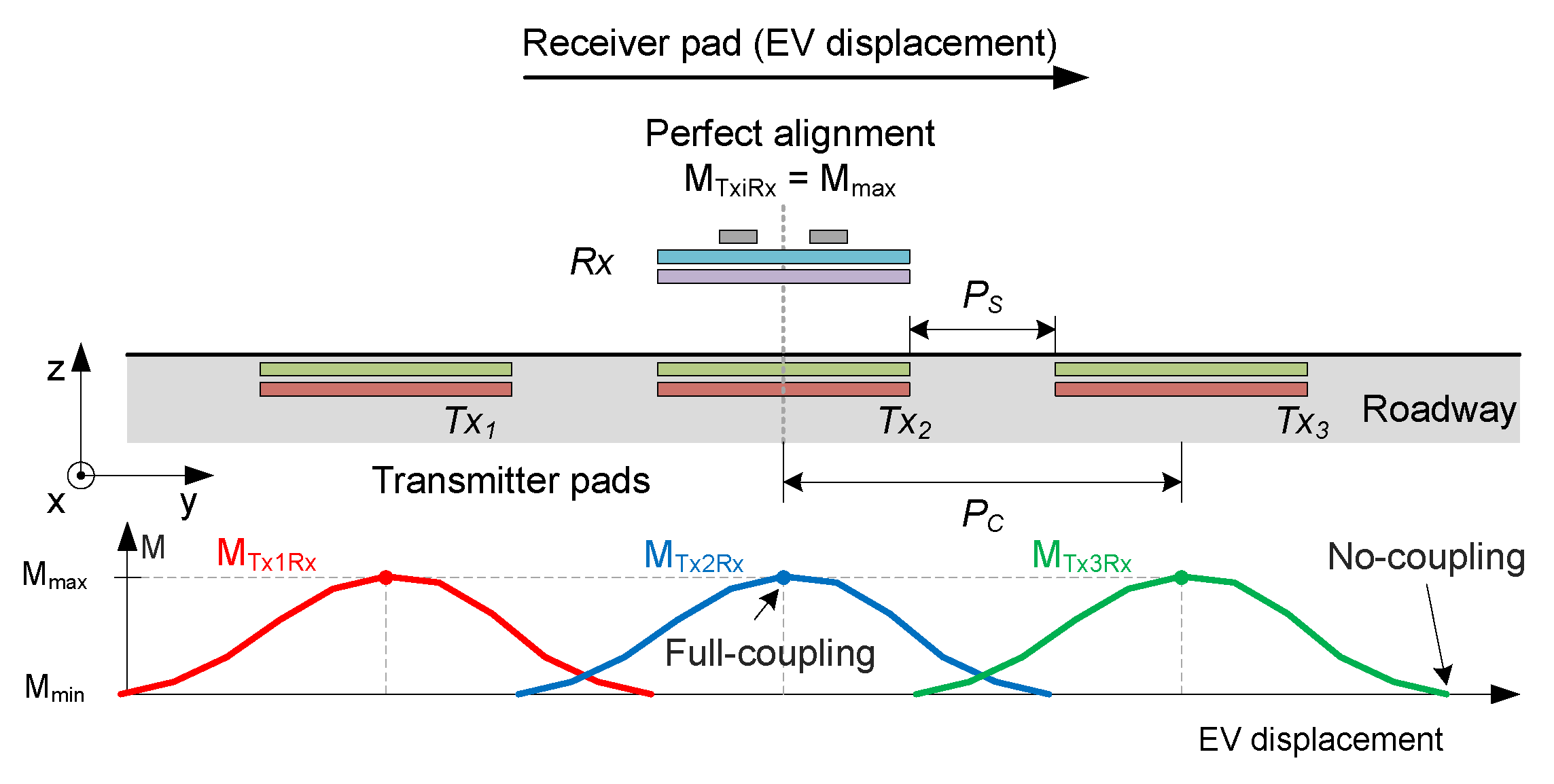
To implement a DIPT system, multiple transmitters are used to form a charging lane on the roadway [9,25,26]. A typical DIPT pad placement is presented in the top part of Figure 2, where multiple transmitter pads are embedded on the roadway. A mutual inductance between each transmitter and the receiver is referred to as M T x i R x , where i = 1 , 2 , 3 , refers to each transmitter T x and R x refers to the receiver pad placed onboard the EV chassis.
A Bipolar pad (BPP) topology is selected, since it allows high tolerance for lateral misalignments [3]. The reference to BPP is related to the MC coils shape and relative position, as in Figure 1a. Three consecutive transmitter pads, represented in red and green, are spaced at distance P c , and one receiver pad, represented in blue and purple, is considered in this analysis. The gray rectangles represent the ferrite cores in the receiver pad, used to improve the MC coupling factor. As the EV moves in the y axis, the energy is transferred from each consecutive transmitter to the receiver. This means that the coupling will follow the bell-shaped pattern that will be repeated in a consecutive way, as shown in the bottom part of Figure 2. If two consecutive transmitters are close enough to each other and are simultaneously energized, the energy transferred to the receiver may be a contribution of these two transmitter pads. Thus, higher distances between consecutive pads lead to points where there is no coupling between any transmitter and the receiver, leading to a no-power-transfer situation. This means that the peak of the M T x i R x curves in Figure 2 will be closer or further apart, depending on the distance P c , which implies a decrease or increase of the minimum achievable coupling between the transmitters and the receiver.
The distance between pads needs to be carefully chosen in order to achieve a certain amount of energy transfer, i.e., energy transfer per km. Furthermore, an increase of the EV speed decreases the time of power transfer between each transmitter and receiver, decreasing the maximum energy transfer capability in a DIPT charging lane. Hence, the EV maximum speed will affect the number of pads needed and the total length of the energized DIPT lane. Moreover, lateral and vertical misalignments will contribute to a lower transfer capability.
In order to assess the applicability of using a specific resonant compensation circuit to dynamic IPT systems, it is necessary to follow a methodological approach. The theoretical analysis starts with considering the electrical circuit of each resonant topology. Kirchhoff’s laws are applied to obtain the different equations in the circuit, assuming the circuit is in steady-state and uses first harmonic approximation (FHA). By rearranging the different mesh equations, it is possible to find voltage and current gain equations, as well as the impedance equations, in different places of the circuit, i.e., the reflected impedance and the input impedance equations, which will be discussed further. This, in the end, will depict the behavior of a certain topology and its applicability on dynamic IPT systems.

2.2. Circuit Considerations and Definitions

Each compensation network circuit is designed to operate at resonance, meaning that the filter natural frequency f 0 is equal to the inverter switching frequency f s , i.e., f 0 = f s . At resonance ω 0 = ω (where ω 0 = 2 π f 0 and ω = 2 π f s ), the imaginary part of the input impedance Z i n is zero; thus, Z i n presents only the real part, behaving as a resistor. When the converter operates at resonance, maximum power transferring capability is achieved, leading to higher overall efficiency. Operating at resonance leads to i T x and i R x having a sinusoidal waveform, although the converter is fed by a square wave voltage. This implies that only the fundamental component of the input voltage, v i n , 1 (1), is responsible for the power transfer to the secondary side, which means using the FHA.
v i n , n = V D C 2 2 π n cos ( α n 2 ) ,
where V D C is the DC bus voltage, n is the n th harmonic, and α is the H-bridge inverter phase-shift (PHS) angle between 0 and 180 .
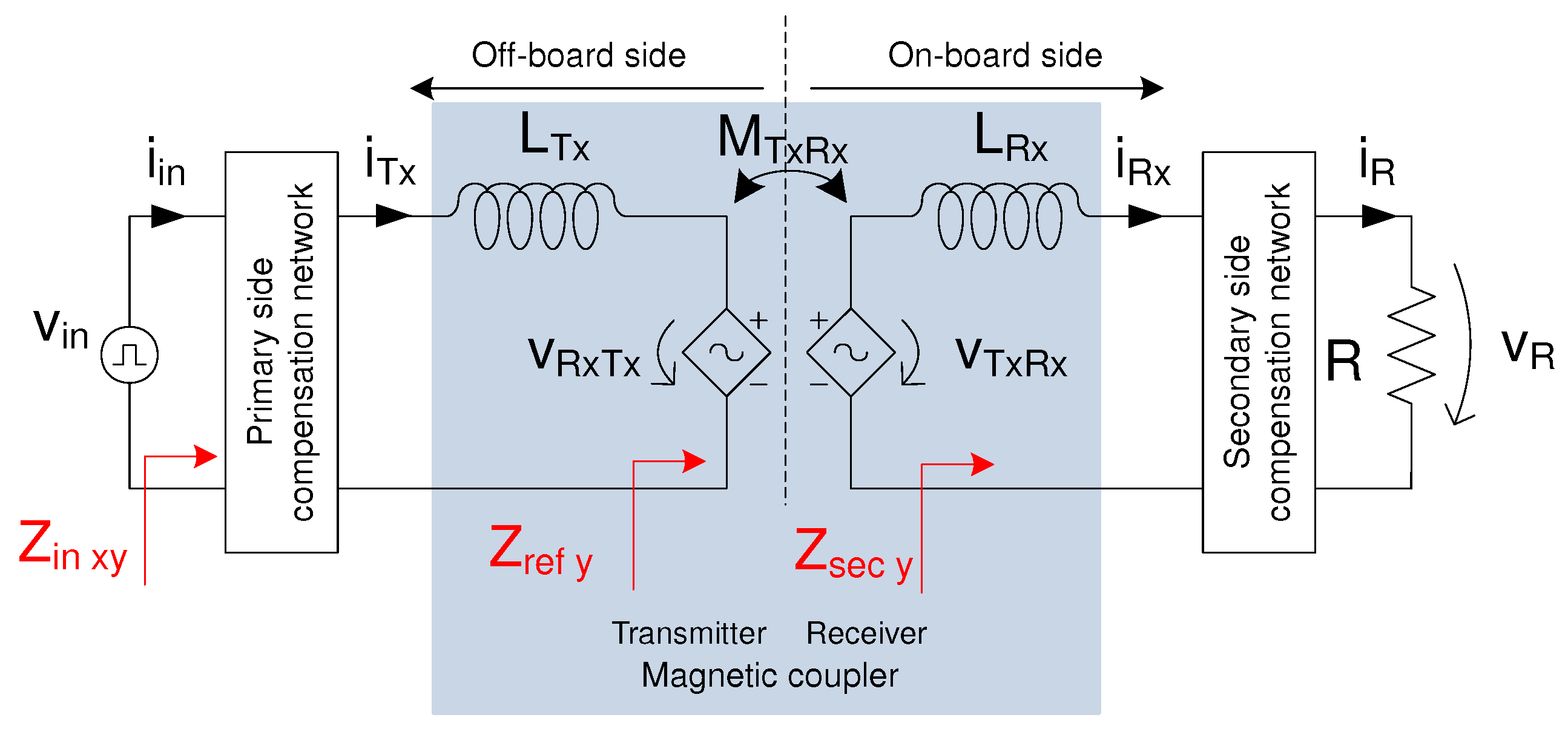
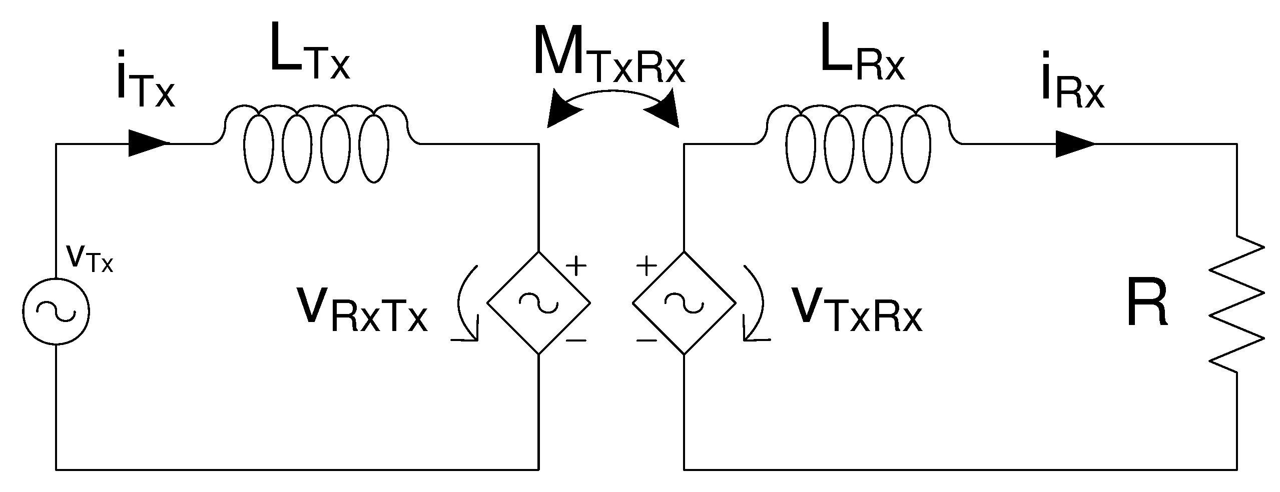
The different resonant networks are modeled with dependent voltage sources and circuit impedances, as shown in Figure 3. An AC equivalent resistor R is typically connected at the output of the secondary-side compensation network, which represents the full-bridge diode rectifier and batteries, where R = 8 π 2 R o . Current i i n is the input current, i T x and i R x are the primary or transmitter and secondary or receiver side currents, respectively, i R and v R are the current and voltage in the equivalent output resistance R, respectively.
Inductors L T x and L R x correspond to the primary and secondary sides’ self-inductance, respectively, and M = M T x R x = M R x T x represents the mutual inductance between the primary and secondary side of the MC. If a comparison is made with an equivalent transformer model, the MC parameters can be obtained using: L T x = L l k p + L m , L R x = L l k s + L m and M T x R x = L m (for unitary transformer ratio), where L l k p and L l k s represent the transformer primary- and secondary-side leakage inductances, respectively, and L m represents the transformer magnetizing inductance. C T x and C R x correspond to the primary- and secondary-side resonant capacitances, respectively, and are placed on the primary and secondary compensation network as in Figure 3. SS, SP, PS, and PP topologies are built by having a resonant capacitor C T x or C R x connected in series or parallel with the primary- or secondary-side coils in the primary- or secondary-side compensation network blocks in Figure 3 [27]. Topologies LCL-S and LCL-P have an extra inductor L i n , added in series with the source v i n . These are the single-coupling topologies analyzed in this work.
Secondary-side impedances are represented by Z s e c y , where y stands for a secondary-side S or P compensation. Voltage v R x T x = j ω M R x T x i R x represents the secondary-side voltage reflected to the primary side and represents the voltage at the terminals of Z r e f y . The reflected impedance is a relation between v R x T x and i T x and can be obtained using Z r e f y = V ¯ R x T x / I ¯ T x . The primary-side voltage reflected to the secondary side is represented by v T x R x = j ω M T x R x i T x . Z i n x y , also in Figure 3, represents the primary-side impedance, where x stands for a primary-side S, P, or LCL compensation. The input impedance is a relation between v i n and i i n and can be obtained using Z i n x y = V ¯ i n / I ¯ i n .

2.3. Impedance Definitions and Resonant Operation

Table 3 presents the reflected impedances Z r e f y and Table 4 presents the input impedances Z i n x y for the various topologies in study. Generic expressions can be used in any load and coupling condition, whereas tuned expressions are only valid in the tuned condition. The tuned condition is the one that is selected for the converter design considering maximum energy transfer capability, perfect alignment, which means maximum mutual inductance or coupling, and nominal load. This implies setting the natural resonance frequency of the system f 0 equal to the converter switching frequency f s . Therefore, for DIPT applications due to the perpetual coupling variation, it is necessary to use the generic equations to assess the circuit behavior.

2.3.1. Secondary-Side Topologies

These are defined as Z s e c S = j ω L R x + 1 j ω C R x + R and Z s e c P = j ω L R x + 1 j ω C R x + 1 R . For tuned and generic conditions, Z r e f y equations are shown in Table 3, considering b R x = ω / ω R x and ω R x = 1 L R x C R x .

2.3.2. Primary-Side Topologies

These are defined as Z i n x y and can be calculated using Z i n S y = j ω L T x + 1 j ω C T x + Z r e f y , Z i n P y = 1 j ω C T x + 1 j ω L T x + Z r e f y and Z i n L C L y = j ω L i n + 1 j ω C T x + 1 j ω L T x + Z r e f y , as in Table 4, where all configurations are specified for generic conditions, considering b T x = ω / ω T x and ω T x = 1 L T x C T x .
Considering Table 3, if the secondary side is operating at resonance, therefore, in tuned conditions, ω R x = ω , which implies that b R x = 1 , and the reflected impedance is simplified as Z r e f T u n e d . For secondary-side S compensation, the imaginary part of Z r e f S is null. In this condition, the load viewed from the primary side is only the real part of the reflected impedance, which depends only on M T x R x and R. This means that load variations affect the input impedance module but not the phase angle (same resonant frequency). Null reactance implies that the tuning of the primary side is independent of the secondary side. ZPA (zero-phase angle) operation is achieved in the primary side, independent of load and coupling conditions.
For a secondary-side P compensation, the imaginary part of Z r e f P is not zero, and the reflected reactance is coupling-dependent. The primary-side compensation will therefore be influenced by this reactance.
If variations of self-inductances are admitted, the tuned condition is lost, and tuned equations are no longer valid, which implies the use of generic equations.
The resonant capacitors values are calculated in order to tune the converter at resonance. To achieve secondary-side resonance, the value of C R x needs to compensate the effect of L R x . For the primary-side resonant capacitor C T x , a similar approach is followed. The goal is to determine C T x to compensate the imaginary part of the input impedance. Nonetheless, depending on the resonant network, the reflected impedance from the secondary side can be different from zero; thus, to achieve a resonant system, C T x needs to compensate both the effect of L T x as well as the imaginary part of Z r e f y .
For SS, SP, PS, and PP topologies, this analysis is well-studied in the literature [28] and the following equations can be used: C R x x y = 1 ω 2 L R x , C T x S S = 1 ω 2 L T x , C T x S P = 1 ω 2 L T x M 2 L R x , C T x P S = L T x ω 2 M 2 R 2 + ω 2 L T x 2 , and C T x P P = L T x M 2 L R x M 2 R L R x 2 2 + ω 2 L T x M 2 L R x 2 .

2.4. Impact of Compensation Networks in DIPT Systems

The previously established generic equations will govern the behavior of the converter. Displacements can lead to high current and voltages in the converter primary side, so converter design and topology are important aspects for conceiving the DIPT system.
Two limit operation conditions will be verified, no-coupling (absence of receiver) and full-coupling conditions. In the no-coupling condition, k T x R x is zero ( M m i n ) , and for full-coupling condition, the perfect alignment between receiver and transmitter, k T x R x , achieves its peak value ( M m a x ) . However, for the full-coupling condition, two different operation conditions may occur, charging and no-charging. Charging happens when the batteries are partially charged (low SoC), and no-charging happens when the batteries are fully charged (SoC 100 % ). The no-charging situation may also occur when the coupling is low ( k T x R x 0 ) . This implies low induced secondary-side voltage and consequently no polarization of the rectifier diodes, leading to no-charging. Curves obtained from the equations in Table 4 allow for the depiction of advantages and disadvantages for each topology as presented.

2.4.1. MC Characterization

The BPP pads’ dimensions are based on the analysis in [3] for a real-size EV application. In this work, for small-scale experimental implementation the dimensions in [3] are reduced by a scale factor of 2 in every dimension. The primary pad is composed of two overlapped coils (red and green in Figure 1). Each coil has 10 turns and 190 × 195 mm (x,y) outer dimensions each, achieving an overall outer dimension of 280 × 195 mm. The secondary pad has the same dimensions, but ferrite cores are added. It has two sets of two 193 × 28 × 16 mm ferrite cores (N87 material), centered in the pad and spaced 30 mm apart (overall core dimensions 186 × 86 mm (x,y)). The distance between transmitter pads P c is 300 mm (approximately 1.5× the pad width of 195 mm).
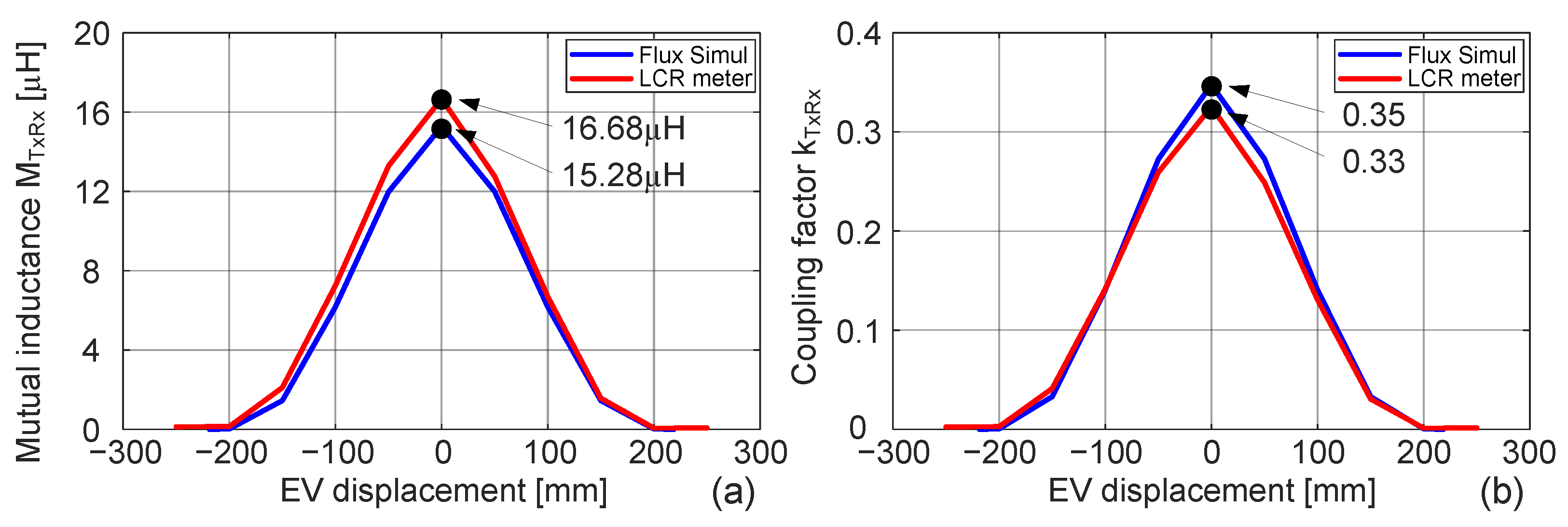
Finite element analysis (FEA) software Flux by Altair is used to characterize the MC in terms of self and mutual inductances, considering one transmitter and one receiver pad. In order to obtain the full characterization when the EV enters until it leaves the transmitter, a simulation scenario is considered for an EV displacement (y axis), from −250 mm to 250 mm with an increment of 50 mm, where position 0 mm correspond to the alignment position between the receiver and the transmitter. A 40 mm airgap between the transmitter and receiver is considered, without lateral misalignments.
From FEA simulations, the self-inductances for the transmitter and receiver pads are L T x = 37.52 μH and L R x = 51.47 μH, respectively. The mutual inductance and coupling factor between the transmitter and receiver, M T x R x and k T x R x curves, as function of the EV displacement are presented in blue in Figure 4.
The simulation starts with a receiver at position −250 mm which means no coupling between the transmitter and receiver, whereby M T x R x and k T x R x equal zero. As the EV moves, the peak coupling corresponds to the position of perfect alignment with the transmitter, at position 0 mm.

2.4.2. Assessment of Compensation Network Behavior

The goal is to assess variations of DIPT compensation networks under load, no-load, and coupling variations (displacement). A similar analysis can also be performed considering a different MC topology.
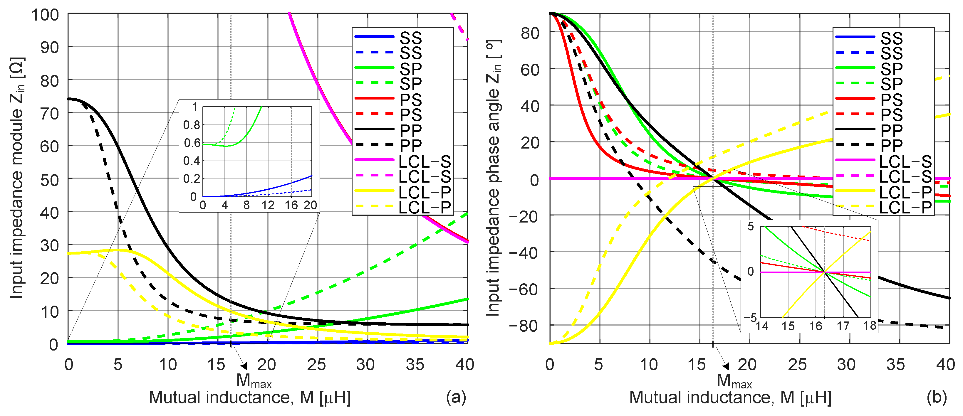
Figure 5 presents the input impedance, Z i n x y , module and phase angle, as function of M T x R x , for the different analyzed topologies. Figure 6 presents the transconductance and voltage gain curves as function of M T x R x , G i T x v i n , and G v R v i n , respectively. All solid lines are referred to nominal load R while the dashed lines refer to 3 R . In the x axis, the value of M m a x represents the maximum M T x R x value, obtained at perfect alignment condition (peak value in Figure 4). All topologies are designed considering the same MC parameters, input voltage v i n , and load R.
From Figure 5, for low/no-coupling conditions, Z i n S S tends to zero, leading to high primary-side currents, which can cause converter failure, while Z i n S P tends to a low value different from zero, limiting the primary-side current. For primary-side P topologies, Z i n P S generates high primary-side voltages, which can cause converter failure, while Z i n P P tends to a relatively high value, which can limit the primary-side voltage but to very high values, also leading to converter failure. This leads to the exclusion of SS, PS, and PP for DIPT. For primary-side LCL topologies, Z i n L C L S tends to a high value (pink curve in Figure 5a), resulting in very low primary-side currents, while for Z i n L C L P , it is limited (yellow curve in Figure 5a), with i i n tending toward a nonzero value. This means that, for LCL-S topology, the primary-side current tends to zero in no-load and no-coupling conditions, which corresponds to a safe operation, reducing converter losses. For SP and LCL-P, having a controllable primary current between maximum safe operating values may be advantageous.
From Figure 5b, the φ Z i n x y analysis shows that LCL-S allows ZPA, meaning resonance operation throughout the operating range of load and coupling, while SP and LCL-P resonance depends on both load and coupling values. Based on the FHA, i i n should be sinusoidal and in phase with the v i n . Nonetheless, if a full-bridge inverter is used to feed the resonant circuit (square wave voltage), the obtained current waveforms will depend on the topology. For SP topology, both i i n and i T x are sinusoidal; however, for primary-side LCL topologies, i T x is sinusoidal, but i i n is not, which means the converter shall not be at resonance even in perfect alignment thus, ZPA is not verified. An adjustment can be made to the inverter phase-shift angle of 120 , in order to reduce the THD, improving the converter overall efficiency [29].
From the transconductance gain in Figure 6a, only PS, LCL-S, and LCL-P allow a constant current i T x feeding the transmitter pad, independent of load variations (overlapped R and 3 R curves), in the coupling range of operation. From Figure 6b, it is possible to see that LCL-S topology can achieve CV mode due to load-independent voltage gain (overlapped R and 3 R curves), in the coupling range of operation.
The compensation topology should provide a natural controllable primary-side current and voltage below maximum rating values without affecting the converter. Based on the analysis, assuming the same MC parameters and input voltage level, SS, PS, and PP will lead to converter failure in the case of no-load and no-coupling operation. Since this is a natural occurrence in DIPT, they can be immediately excluded. Regarding SP topology, it allows high power transfer without compromising converter safe operation (when compared to SS null input impedance at no-coupling condition). Nonetheless, for low- and no-coupling conditions, i i n will be higher than at the full-coupling condition. This is undesirable since these coupling conditions will happen the majority of the time, due to the EV being above the transmitter pad only for a short period. Primary-side LCL topologies achieve constant transmitter current i T x . Nonetheless, LCL-P resonant operation is affected by mutual and/or load variations, allowing relatively low power transfer. Although operating at resonance at maximum coupling, the remaining operating range is only at ZCS (zero-current switching) mode, which can lead to voltage spikes in the resonant inverter. LCL-S may be a possibility due to ZPA, although at the cost of relatively low power transfer. Nonetheless, this topology does not allow galvanic isolation between the HF inverter and the MC transmitter pad, which is an important issue in EV charging systems.

3. Double-Coupling Resonant Network for DIPT System

Considering the advantages of the single-coupling SS topology, such as resonant compensation circuit simplicity, high power transfer, load- and coupling-independent resonant operation, an extra magnetic coupler (isolation transformer) is added to the SS circuit. This extra magnetic coupler provides galvanic isolation between the inverter and the MC transmitter pad and simultaneously limits the current i i n to predefined values, whereas i i n S S . Considering series compensation in the additional circuit mesh, the double-coupling SSS is obtained. The new magnetic coupler (MC1) has a constant coupling factor, whereas the second MC (MC2) exhibits the well-known bell-shaped curved, discussed in the previous sections. The intrinsic characteristics and advantages for DIPT applications of the series-series-series (SSS) configuration will be subsequently analyzed.

3.1. Circuital Analysis

Figure 7a illustrates the equivalent model of a double-coupling SSS, for the fundamental harmonic, where the magnetic couplers are identified as MC1 and MC2. The equivalent voltage supply ( V ¯ i n ) is connected to the transmitter coil of MC1 by means of a series capacitor, C a . The receiver coil of MC1 is also connected with a series capacitor C T x , to the transmitter coil of the MC2. On the vehicle side, the classical series compensation network is used, with capacitor C R x .
By applying Kirchhoff’s circuit laws to the SSS equivalent circuit, the following equations are obtained:
V ¯ i n = r a I ¯ a + j ω ( ( L a 1 / ( ω 2 C a ) ) I ¯ a M a b I ¯ b ) ,
0 = ( r b + r T x ) I ¯ b + j ω ( ( L b + L T x 1 / ( ω 2 C T x ) ) I ¯ b M a b I ¯ a M T x R x I ¯ R x ) ,
0 = ( R + r R x ) I ¯ R x + j ω ( ( L R x 1 / ( ω 2 C R x ) ) I ¯ R x M T x R x I ¯ b ) ,
where L a and L b are the self-inductances of MC1 and L T x and L R x are the self-inductances of MC2. The subscript in the variables indicate to which side the variable is related, where a and R x stand for MC1 primary and MC2 receiver sides respectively, while b and T x stand for the intermediary side (MC1 secondary and MC2 transmitter). The mutual inductances M a b and M T x R x quantify the magnetic link of the MC1 and MC2, respectively. The parameters r a , r b , r T x , and r R x denote the equivalent resistance of each pad and they include the Joule and iron (if applicable) losses. The capacitors’ values are given by C a = 1 / ( ω a 2 · L a ) , C T x = 1 / ( ω b 2 · ( L b + L T x ) ) , and C R x = 1 / ( ω R x 2 · L R x ) , where ω a , ω b , and ω R x are the angular resonant frequencies of the resonant tanks. Solving (2) to (4) provides the current equations that accurately define the SSS model:
I ¯ a = V ¯ i n , 1 ( Z a + Z r e f b ) ,
I ¯ b = I ¯ T x = I ¯ a j ω M a b Z b + Z r e f R x ,
I ¯ R x = I ¯ R = I ¯ b j ω M T x R x Z R x + R ,
where Z a , Z b , and Z R x are the equivalent impedance values of the resonant tanks in the transmitter, intermediary, and receiver sides, respectively, and they are given by
Z a = r a + j ω L a ( 1 1 / b a 2 ) ,
Z b = ( r b + r T x ) + j ω ( L b + L T x ) ( 1 1 / b b 2 ) ,
Z R x = r R x + j ω L R x ( 1 1 / b R x 2 ) .
The variables b a , b b , and b R x , described in (11), are relation factors between the system angular operating frequency ω and the angular resonant frequencies of the transmitter ( ω a ), intermediate ( ω b ), and receiver ( ω R x ) resonant tanks. A unitary relation factor at the fundamental frequency means ω = ω x , while a relation lower than 1 means ω < ω x , where the subscript x represents different sides, a, b, or R x .
b a = ω / ω a , b b = ω / ω b , b R x = ω / ω R x .
A double-coupling system has two reflected impedance values, as illustrated in Figure 7a. The reflected impedance from the receiver side onto the intermediary side ( Z r e f R x ) is equivalent to a single-coupling IPT system, discussed in Section 2 ( Z r e f R x = Z r e f S in Table 3). The reflected impedance from the intermediary side onto the transmitter side ( Z r e f b ), on the other hand, is given in (12).
Z r e f b = V ¯ b a I ¯ a = ω 2 M a b 2 ( Z R x + R ) Z b ( Z R x + R ) + ω 2 M T x R x 2 .
Assuming an ideal and perfect tuned system, (12) can be simplified into the equation described in (13). The value of Z r e f b , in such conditions, is purely resistive and the value of R is simply affected by a factor of M a b 2 / M T x R x 2 .
Z r e f b = M a b 2 R M T x R x 2 + j 0 .

3.2. Load, No-Load, and Coupling Impact for the SSS Configuration

A distinctive characteristic of DIPT systems is the displacement of the EV over a transmitter pad in a short amount of time, resulting in a bell-shape coupling variation of the MC2, as already illustrated in Figure 2. Consequently, the SSS configuration must perform adequately under the two limit operation conditions previously identified, no-coupling (absence of receiver) and full-coupling.

3.2.1. No-Coupling Mode

During the EV absence, it is important to ensure that the inverter current is kept at the lowest possible value, thus minimizing the system losses. Moreover, I i n should decrease/increase naturally, within acceptable range, to avoid risks of over-current in the overall circuitry.
The absence of receiver leads to a null induced voltage V ¯ R x T x and the remaining circuit corresponds to a classical SS resonant configuration, as illustrated in Figure 7b. As such, and assuming that ω a = ω b = ω , the value of Z i n S S at the fundamental frequency will be large, according to the function depicted in Table 4. However, the impact of the odds harmonics of V i n in I ¯ a must be taken into account and their value minimized by ensuring a high Z i n S S at those frequencies. Figure 8a shows the amplitude of Z i n S S as a function of the frequency for different self and mutual inductance values in MC1, and the corresponding 3rd, 5th, and 7th harmonic frequencies are marked as well. The solid lines identify a k a b in MC1 equal to 0.6 with different self-inductance values (ranging between 20 μ H and 60 μ H). The dashed lines, on the other hand, correspond to k a b = 0.9 with the same self-inductance values of the solid lines. All curves exhibit inflection points that mark the transition from a capacitive to inductive impedance of Z i n . Until this inflection point, the reflected capacitive reactance is predominant in comparison with the inductive reactance of the transmitter network (when ω > ω a , the LC network is inductive). The analysis of Figure 8a results in:
(i)
The use of an MC1 with larger self-inductance values results in higher | Z i n S S | values at the harmonic frequencies, and consequently, it reduces the corresponding current component values;
(ii)
The increase of k a b moves the inflection point closer to the harmonic frequencies. Therefore, high coupled MC1 will exhibit larger I ¯ a values due to the harmonic values, especially the 3rd and 5th components.
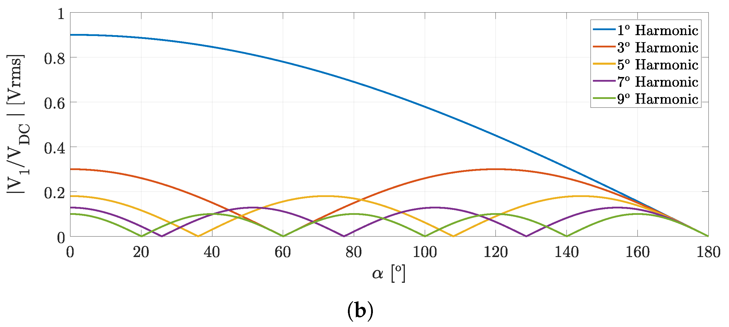
One way to mitigate the impact of the 3rd harmonic component is by simply operating the H-bridge inverter with a 60 angle instead of 0 . In this way, the amplitudes of V i n of the 3rd and 9th harmonics are null, as illustrated in Figure 8b. Therefore, MC1 can have higher k a b values since the 3rd component has no impact in the final value of I ¯ a .

3.2.2. Coupling Mode

The vehicle’s passing over the transmitter pad of the MC2 initiates the charging process of the EV battery pack. In this scenario, the equivalent model corresponds to a double-coupling SSS configuration, as illustrated in Figure 7a. A more detailed mathematical analysis was carried out in [23] with special emphasis on voltage and transconductance gain functions. The transmitter current of MC2 ( I ¯ T x ), described in (6), in tuned conditions is simplified into
I ¯ T x , 1 = j V ¯ i n , 1 ω M a b .
According to (14), I ¯ T x depends on the H-bridge inverter voltage, ω , and mutual inductance of MC1. Therefore, the SSS configuration acts as a constant current source in the intermediary resonant network, with little effect under the load and MC2 coupling variations.
The current passing through the inverter, given by (5), in tuned conditions is described by:
I ¯ a , 1 = V ¯ i n , 1 M T x R x 2 M a b 2 R .
According to (15), the power transferred to the load is dependent on the mutual inductance values ratio of MC2 and MC1 as well as the the H-bridge inverter voltage. Since M a b is approximately constant and M T x R x decreases due to the movement of the EV, the value of I ¯ a , 1 is limited naturally by the intrinsic characteristics of the SSS configuration. Furthermore, in a charging scenario with a coupled vehicle but with the batteries fully charged ( R = ), I ¯ a , 1 is also limited, as the equivalent circuit model matches the no-coupling mode (SS configuration).
To summarize, the main features of the SSS configuration are as follows:
  • Current source characteristics in the intermediary network ( I b );
  • Load-independent voltage source characteristics between output/input voltages ( V R / V i n );
  • Load/no-load: limits I i n ;
  • Coupling/no-coupling: limits I i n ;
  • ϕ Z i n coupling and load-independence.
The main characteristics of the different resonant topologies analyzed are summarized in Table 5, highlighting the main features and behavior of each compensation network and its suitablity for DIPT applications.

4. MC Model and Simulation Results

The DIPT system is simulated using MATLAB/Simulink in order to emulate its behavior under different EV displacement and load conditions as in Figure 9 for a double-coupling SSS topology. To emulate the M T x R x behavior under EV displacement, MC2 is modeled using the MC model as in Figure 10, where v R x T x = j ω M R x T x i R x and v T x R x = j ω M T x R x i T x . Controlled voltage sources are used to achieve the effect of M T x R x variation, with v R x T x = M R x T x d i R x d t and v T x R x = M T x R x d i T x d t . The MC2 parameters L T x and L R x are kept constant and a mutual inductance profile between the transmitter and receiver pad is considered via a 2D lookup table (with the values from Figure 4a) in the block Position → Mutual inductance, in Figure 9. The block has two inputs, Speed [km/h] and Initial position [mm]. The first input is the EV speed and the second input is the initial position of the onboard receiver pad, relative to the transmitter pad. An initial position of 0 mm represents perfect alignment between receiver and transmitter pads, as in Figure 1b. It has two outputs, Mutual inductance [ μ H] and Position [mm], which correspond to the EV position and correspondent M T x R x at that position. The second added MC (MC1) is simulated using a Mutual Inductance block with the parameters L a , L b , and M a b .
The different parameters are presented in Table 6. To minimize the input current harmonics according to the analysis in Section 3, the MC1 coupling is selected to be k a b = 0.72 in the SSS circuit.
The simulation assumes a constant EV speed during 180 ms with the coupling variation, according to Figure 4, and a load step at 90 ms, from R o = 2.4 Ω to open-circuit. The coupling factor starts to increase at 200 mm (20 ms in Figure 11) and the instant 90 ms corresponds to the perfect alignment position of 0 mm in Figure 4. The results in terms of primary- and secondary-side voltages and currents are presented in Figure 11 and confirm the expected theoretical analysis for the classical single-coupling SS topology and for the double-coupling SSS topology. For the classical SS topology, i i n = i T x due to primary-side series connection. For the no- and low-coupling situation, the current tends to a high value, limited by the wires series resistance and tends to a minimum value at full coupling, which corresponds to 90 ms (corresponding to 0 mm in Figure 4).
Theoretically, from Figure 5a, Z i n 0 , which leads to i i n , exceeding maximum current rated values. Conversely, for double-coupling SSS topology, both the input current i i n and the intermediate current i T x are always kept under maximum values.
It is important to say that these results assume similar conditions in terms of input DC bus, MC2, and load R o . No dedicated design is made, however, from this analysis it is already possible to assess the adequate behavior of the double-coupling SSS configuration for DIPT applications.

5. Experimental Validation

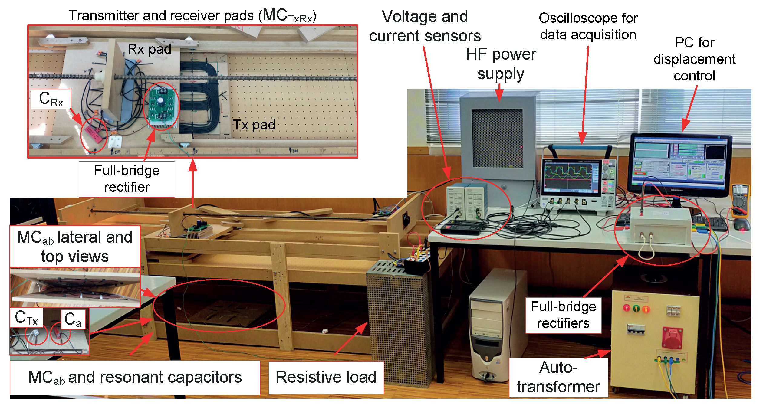
A small-scale prototype of a DIPT system, presented in Figure 12, was built and used to validate the previous analysis, considering the specifications in Table 6, for the double-coupling SSS topologies. The top picture depicts the transmitter and the receiver pads as well as the secondary-side resonant capacitor. The bottom picture depicts a structure with the transmitter and receiver pads (MC2) to emulate EV displacement, controlled with a step-motor. The transmitter side resonant components are placed under the structure and are connected accordingly to the double-coupling SSS (MC1, C a , and C T x ). On the right side, the DC bus is generated via a rectifier fed by an autotransformer and the electrical grid. The H-bridge inverter uses C3M0065090D SiC MOSFETs controlled with a DSP from Texas Instruments TMS320F28335 and gate drivers PT62SCMD12 from CREE/Wolfspeed. Tektronix oscilloscope and voltage and current probes are used to obtain the experimental results. The receiver is connected to the secondary-side resonant capacitor in series, followed by an high-frequency full-bridge rectifier and resistive load R o . The magnetic couplers MC1 and MC2 characterization is made using an LCR Meter BK PRECISION 889A. For MC2, the mutual inductance and coupling, M T x R x and k T x R x , curves as function of the EV displacement were previously presented in Figure 4, where the blue curves represent the simulation results from FEA analysis and the red curves represent the experimental results measured with the LCR meter.
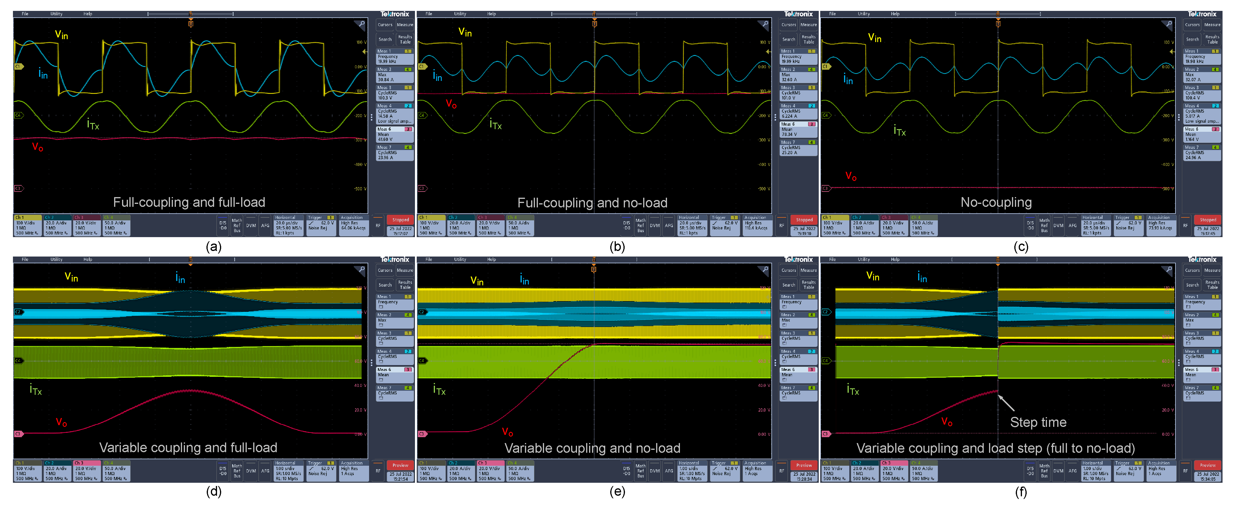
The experimental results for the double-coupling SSS topology showing the behavior under EV displacement and the operation under full- and no-coupling and full- and no-load conditions are presented in Figure 13. The yellow and blue waveforms represent the input voltage and current, v i n and i i n , respectively. The pink waveform represents the output voltage v o at the load terminals R o and the green waveform represents the intermediate current i b = i T x in the resonant capacitor C T x .
Figure 13a presents the results with full-coupling condition for full-load ( R o = 2.4 Ω ) and Figure 13b presents the results with full-coupling condition for no-load ( R o = ). Figure 13c presents the results for no-coupling. Both the input current i i n and transmitter current i T x are always limited under these conditions. As expected, the impact of the square wave harmonic content v i n leads to a non-sinusoidal input current i i n , confirming the theoretical analysis in Section 3. Under the no-coupling condition, without vehicle, i i n stabilizes at a certain value different from zero, in this case around 5 A, which ensures safe converter operation in the low- and no-coupling conditions as desired. Moreover, i T x remains approximately constant, in this case, around 24 A, independent of coupling and load, which is the feature expected for the double coupling SSS topology. At the full-coupling and full-load condition, v o (and consequently i o ) tends to the maximum value, and for no-coupling, it tends to zero.
Considering variable coupling, shown in Figure 13d, it can clearly be seen that v o exhibits the expected bell-shaped behavior and that i i n and i T x are limited throughout the operating range. The output current i o will have the same waveform as the output voltage v o , since a resistive load is used to emulate the EV battery pack. Considering the no-load condition as in Figure 13e, i i n and i T x remain limited throughout the operating range and v o will represent the charging of the output capacitor at the rectifier output and the i o will be zero (no-load). Figure 13f presents the results with variable coupling and considering a load step from R o = 2.4 Ω to open-circuit (no-load condition). The expected behavior can be seen, as in the simulation results in Figure 11, where i i n and i T x are kept limited under full operating range, for full- and no-coupling and for full- and no-load conditions, making the double-coupling SSS topology a solution for DIPT applications, while providing additional galvanic isolation between the HF inverter and the MC2 transmitter pad, compared to single-coupling topologies. This is advantageous for DIPT systems, since it improves the users’ safety.
The input current i i n is not sinusoidal due to the v i n harmonics (square wave voltage), although this effect can be minimized if the inverter phase-shift angle is adjusted to 120 , allowing for the reduction of the current THD, improving the converter overall efficiency, as analyzed in Section 3 [29]. With the receiver movement in the y axis, there is power transfer and the primary-side currents are limited throughout the operating range. If lateral misalignments occur, the same behavior is expected for both topologies, since the MC mutual inductance and coupling factor will exhibit the same bell-shaped curve behavior as in Figure 2. However, the maximum achievable coupling M T x R x decreases with the lateral misalignment, resulting in lower power transfer.
In order to evaluate the methodology, the theoretical (mathematical calculations), simulation, and experimental results are presented in Table 7.
The results are presented considering full-coupling and full-load steady state condition. It is possible to verify that the error between simulation and theoretical results is below 10% for the different values I i n , I T x , and V o . Notice that the mathematical equations use FHA while the simulation model includes the harmonic content of the square wave input voltage, v i n , and the influence of the output rectifier. Therefore, the obtained errors are considered reasonable. For the experimental results relative to the simulation model, a maximum error below 15% is obtained, which validates the analysis presented.

6. Conclusions

This paper compares different resonant topologies for DIPT application. Due to the dynamic motion of the EV, the impact of coupling and load variations in the converter operation are analyzed, considering the same DC bus, MC, and load parameters. Compared to SIPT systems, DIPT systems have additional requirements regarding the selection of the compensation network, particularly due to no-coupling and no-load intermittent conditions, while ensuring a safe converter operation. Thus, using a resonant topology with natural behavior which already limits current and voltage below safety values is preferable. Additional control techniques could be added to improve converter operation and power transfer. Since, in DIPT, the EV is moving at a certain speed, the coupling variation can happen rapidly, which means that a very-high-speed controller would be needed. Two controllers would probably be needed, one placed onboard, responsible for the control of the energy delivered to the batteries, and the other one placed off-board, responsible for transmitter side current and voltage control. This adds complexity to the system regarding the need for additional communication layers and sensors, which could be avoided if the converter topology exhibits natural safe behavior.
Regarding the commonly used SS topology in SIPT, although it has load-independent resonant operation, in DIPT application it will give a non-controllable input current. PS and PP topologies will have a similar characteristic but in terms of input voltage, making them unsuitable for DIPT applications. Adding to this, they would need an extra large choke inductor in the DC bus to achieve current source characteristics in the inverter to feed the primary-side P circuit. LCL-S, LCL-P, and SP topologies are suitable for DIPT systems, but nonetheless present some limitations. For low- and no-coupling conditions, using SP topology will result in the input current higher than at full-coupling condition, which is undesirable since these coupling conditions will occur often. For LCL-P topology, resonant operation is affected by both coupling and load variations and has relatively low power transfer. Operation in ZCS mode can lead to undesirable voltage spikes in the resonant inverter. LCL-S topology allows ZPA operation, but it presents relatively low power transfer and the input current is not sinusoidal when the converter is fed by a square voltage source. To overcome some limitations of previous topologies, a double-coupling SSS topology is proposed for DIPT application. Similar to the classical SS topology, it allows load-independent resonant operation while limiting primary-side currents under no-load and no-coupling conditions. It allows safe operation under the whole operating range of load and coupling, from full- to no-load and full- to no-coupling conditions, making it suitable for DIPT applications. It allows a relatively simple design due to the use of simple series compensation networks and ensures inherent galvanic isolation between the inverter and the transmitter pad due to an extra magnetic coupler or isolation transformer. Considering the obtained results in this work, it is possible to conclude that the experimental results relative to the theoretical ones present an error below 10%, and for the experimental results relative to the simulation results, the error is below 15%, thus validating the presented analysis.

Author Contributions

Conceptualization, V.S.C., E.M., M.S.P. and A.M.S.M.; validation, V.S.C. and E.M.; formal analysis, V.S.C. and E.M.; investigation, V.S.C. and E.M.; resources, V.S.C. and A.M.S.M.; data curation, V.S.C.; writing—original draft, V.S.C. and E.M.; writing—review and editing, V.S.C., E.M., M.S.P. and A.M.S.M.; visualization, V.S.C.; supervision, M.S.P. and A.M.S.M.; project administration, A.M.S.M. All authors have read and agreed to the published version of the manuscript.

Funding

This work was supported by the PhD scholarship with reference SFRH/BD/138841/2018, Instituto de Telecomunicações Project inWheel-IPT with reference 2022.06192.PTDC, and Project UIDB/50008/2020 and Project UIDP/50008/2020 all funded by the Portuguese Foundation for Science and Technology (FCT—Fundação para a Ciência e a Tecnologia).

Institutional Review Board Statement

Not applicable.

Informed Consent Statement

Not applicable.

Data Availability Statement

Not applicable.

Conflicts of Interest

The authors declare no conflict of interest. The funders had no role in the design of the study; in the collection, analyses, or interpretation of data; in the writing of the manuscript, or in the decision to publish the results.

Abbreviations

The following abbreviations are used in this manuscript:
ACAlternate Current
BPPBipolar Pad
CCConstant Current
CVConstant Voltage
DCDirect Current
DIPTDynamic Inductive Power Transfer
EVElectric Vehicle
FEAFinite Element Analysis
FHAFirst Harmonic Approximation
HFHigh-Frequency
IPTInductive Power Transfer
MCMagnetic Coupler
PParallel
PPParallel-Parallel
PSParallel-Series
SIPTStatic Inductive Power Transfer
SSeries
SPSeries-Parallel
SSSeries-Series
SSSSeries-Series-Series
THDTotal Harmonic Distortion
WPTWireless Power Transfer
ZCSZero Current Switching
ZPAZero Phase Angle
ZVSZero Voltage Switching

References

  1. Khalid, M.R.; Khan, I.A.; Hameed, S.; Asghar, M.S.J.; Ro, J.-S. A Comprehensive Review on Structural Topologies, Power Levels, Energy Storage Systems, and Standards for Electric Vehicle Charging Stations and Their Impacts on Grid. IEEE Access 2021, 9, 128069–128094. [Google Scholar] [CrossRef]
  2. Panchal, C.; Stegen, S.; Lu, J. Review of static and dynamic wireless electric vehicle charging system. Eng. Sci. Technol. Int. J. 2018, 21, 922–937. [Google Scholar] [CrossRef]
  3. Marques, E.G.; Mendes, A.M.S. Optimization of transmitter magnetic structures for roadway applications. In Proceedings of the 2017 IEEE Applied Power Electronics Conference and Exposition (APEC), Tampa, FL, USA, 26–30 March 2017; pp. 959–965. [Google Scholar] [CrossRef]
  4. Marques, E.G.; Mendes, A.M.S.; Perdigão, M.S.; Costa, V.S. Design Methodology of a Three Coil IPT System with Parameters Identification for EVs. IEEE Trans. Veh. Technol. 2021, 70, 7509–7521. [Google Scholar] [CrossRef]
  5. Nagendra, G.R.; Chen, L.; Covic, G.A.; Boys, J.T. Detection of EVs on IPT Highways. IEEE J. Emerg. Sel. Top. Power Electron. 2014, 2, 584–597. [Google Scholar] [CrossRef]
  6. Covic, G.A.; Boys, J.T. Inductive Power Transfer. Proc. IEEE 2013, 101, 1276–1289. [Google Scholar] [CrossRef]
  7. Ramezani, A.; Narimani, M. A Dynamic Wireless Charging System with a Robust Output Voltage Respect to Misalignment. In Proceedings of the 2019 IEEE PELS Workshop on Emerging Technologies: Wireless Power Transfer (WoW), London, UK, 18–21 June 2019; pp. 292–296. [Google Scholar] [CrossRef]
  8. Tavakoli, R.; Pantic, Z. ANN-based algorithm for estimation and compensation of lateral misalignment in dynamic wireless power transfer systems for EV charging. In Proceedings of the 2017 IEEE Energy Conversion Congress and Exposition (ECCE), Cincinnati, OH, USA, 1–5 October 2017; pp. 2602–2609. [Google Scholar] [CrossRef]
  9. Barsari, V.Z.; Thrimawithana, D.J.; Covic, G.A. An Inductive Coupler Array for In-Motion Wireless Charging of Electric Vehicles. IEEE Trans. Power Electron. 2021, 36, 9854–9863. [Google Scholar] [CrossRef]
  10. Karakitsios, I.; Palaiogiannis, F.; Markou, A.; Hatziargyriou, N.D. Optimizing the Energy Transfer, With a High System Efficiency in Dynamic Inductive Charging of EVs. IEEE Trans. Veh. Technol. 2018, 67, 4728–4742. [Google Scholar] [CrossRef]
  11. Jeong, S.Y.; Park, J.H.; Hong, G.P.; Rim, C.T. Autotuning Control System by Variation of Self-Inductance for Dynamic Wireless EV Charging with Small Air Gap. IEEE Trans. Power Electron. 2019, 34, 5165–5174. [Google Scholar] [CrossRef]
  12. Gati, E.; Kampitsis, G.; Manias, S. Variable Frequency Controller for Inductive Power Transfer in Dynamic Conditions. IEEE Trans. Power Electron. 2017, 32, 1684–1696. [Google Scholar] [CrossRef]
  13. Kamineni, A.; Covic, G.A.; Boys, J.T. Interoperable EV detection for dynamic wireless charging with existing hardware and free resonance. In Proceedings of the 2016 IEEE PELS Workshop on Emerging Technologies: Wireless Power Transfer (WoW), Knoxville, TN, USA, 4–6 October 2016; pp. 169–173. [Google Scholar] [CrossRef]
  14. Wang, C.H.; Stielau, O.H.; Covic, G.A. Design considerations for a contactless electric vehicle battery charger. IEEE Trans. Ind. Electron. 2005, 52, 1308–1314. [Google Scholar] [CrossRef]
  15. Shevchenko, V.; Husev, O.; Strzelecki, R.; Pakhaliuk, B.; Poliakov, N.; Strzelecka, N. Compensation Topologies in IPT Systems: Standards, Requirements, Classification, Analysis, Comparison and Application. IEEE Access 2019, 7, 120559–120580. [Google Scholar] [CrossRef]
  16. Patil, D.; McDonough, M.K.; Miller, J.M.; Fahimi, B.; Balsara, P.T. Wireless Power Transfer for Vehicular Applications: Overview and Challenges. IEEE Trans. Transp. Electrif. 2018, 4, 3–37. [Google Scholar] [CrossRef]
  17. Sonapreetha, M.R.; Jeong, S.Y.; Choi, S.Y.; Rim, C.T. Dual-purpose non-overlapped coil sets as foreign object and vehicle location detections for wireless stationary EV chargers. In Proceedings of the 2015 IEEE PELS Workshop on Emerging Technologies: Wireless Power (2015 WoW), Daejeon, Republic of Korea, 5–6 June 2015; pp. 1–7. [Google Scholar] [CrossRef]
  18. Wang, H.; Pratik, U.; Jovicic, A.; Hasan, N.; Pantic, Z. Dynamic Wireless Charging of Medium Power and Speed Electric Vehicles. IEEE Trans. Veh. Technol. 2021, 70, 12552–12566. [Google Scholar] [CrossRef]
  19. Barsari, V.Z.; Thrimawithana, D.J.; Covic, G.A.; Kim, S. A Switchable Inductively Coupled Connector for IPT Roadway Applications. In Proceedings of the 2020 IEEE PELS Workshop on Emerging Technologies: Wireless Power Transfer (WoW), Seoul, Republic of Korea, 15–19 November 2020; pp. 35–39. [Google Scholar] [CrossRef]
  20. Chen, L.; Nagendra, G.R.; Boys, J.T.; Covic, G.A. Double-Coupled Systems for IPT Roadway Applications. IEEE J. Emerg. Sel. Top. Power Electron. 2015, 3, 37–49. [Google Scholar] [CrossRef]
  21. Wireless Power Transfer for Light-Duty Plug-In/Electric Vehicles and Alignment Methodology; SAE International: Warrendale, PA, USA, 2016.
  22. Feng, H.; Cai, T.; Duan, S.; Zhao, J.; Zhang, X.; Chen, C. An LCC-Compensated Resonant Converter Optimized for Robust Reaction to Large Coupling Variation in Dynamic Wireless Power Transfer. IEEE Trans. Ind. Electron. 2016, 63, 6591–6601. [Google Scholar] [CrossRef]
  23. Marques, E.G.; Costa, V.S.; Torres, M.; Rios, B.; Mendes, A.M.S.; Perdigão, M.S. Double Coupling IPT Systems for EV Charging Applications. In Proceedings of the 2021 IEEE Vehicle Power and Propulsion Conference (VPPC), Gijon, Spain, 25–28 October 2021; pp. 1–6. [Google Scholar] [CrossRef]
  24. Wu, H.H.; Gilchrist, A.; Sealy, K.D.; Bronson, D. A High Efficiency 5 kW Inductive Charger for EVs Using Dual Side Control. IEEE Trans. Ind. Inform. 2012, 8, 585–595. [Google Scholar] [CrossRef]
  25. Ahmad, A.; Alam, M.S.; Chabaan, R. A Comprehensive Review of Wireless Charging Technologies for Electric Vehicles. IEEE Trans. Transp. Electrif. 2018, 4, 38–63. [Google Scholar] [CrossRef]
  26. Navidi, T.; Cao, Y.; Krein, P.T. Analysis of wireless and catenary power transfer systems for electric vehicle range extension on rural highways. In Proceedings of the 2016 IEEE Power and Energy Conference at Illinois (PECI), Urbana, IL, USA, 19–20 February 2016; pp. 1–6. [Google Scholar] [CrossRef]
  27. Stielau, O.H.; Covic, G.A. Design of loosely coupled inductive power transfer systems. In Proceedings of the 2000 International Conference on Power System Technology (PowerCon 2000), Proceedings (Cat. No.00EX409), Perth, Australia, 4–7 December 2000; Volume 1, pp. 85–90. [Google Scholar] [CrossRef]
  28. Wang, C.H.; Covic, G.A.; Stielau, O.H. Power transfer capability and bifurcation phenomena of loosely coupled inductive power transfer systems. IEEE Trans. Ind. Electron. 2004, 51, 148–157. [Google Scholar] [CrossRef]
  29. Wu, H.H.; Gilchrist, A.; Sealy, K.; Israelsen, P.; Muhs, J. Design of Symmetric Voltage Cancellation Control for LCL converters in Inductive Power Transfer Systems. In Proceedings of the 2011 IEEE International Electric Machines & Drives Conference (IEMDC), Niagara Falls, ON, Canada, 15–18 May 2011; pp. 866–871. [Google Scholar] [CrossRef]
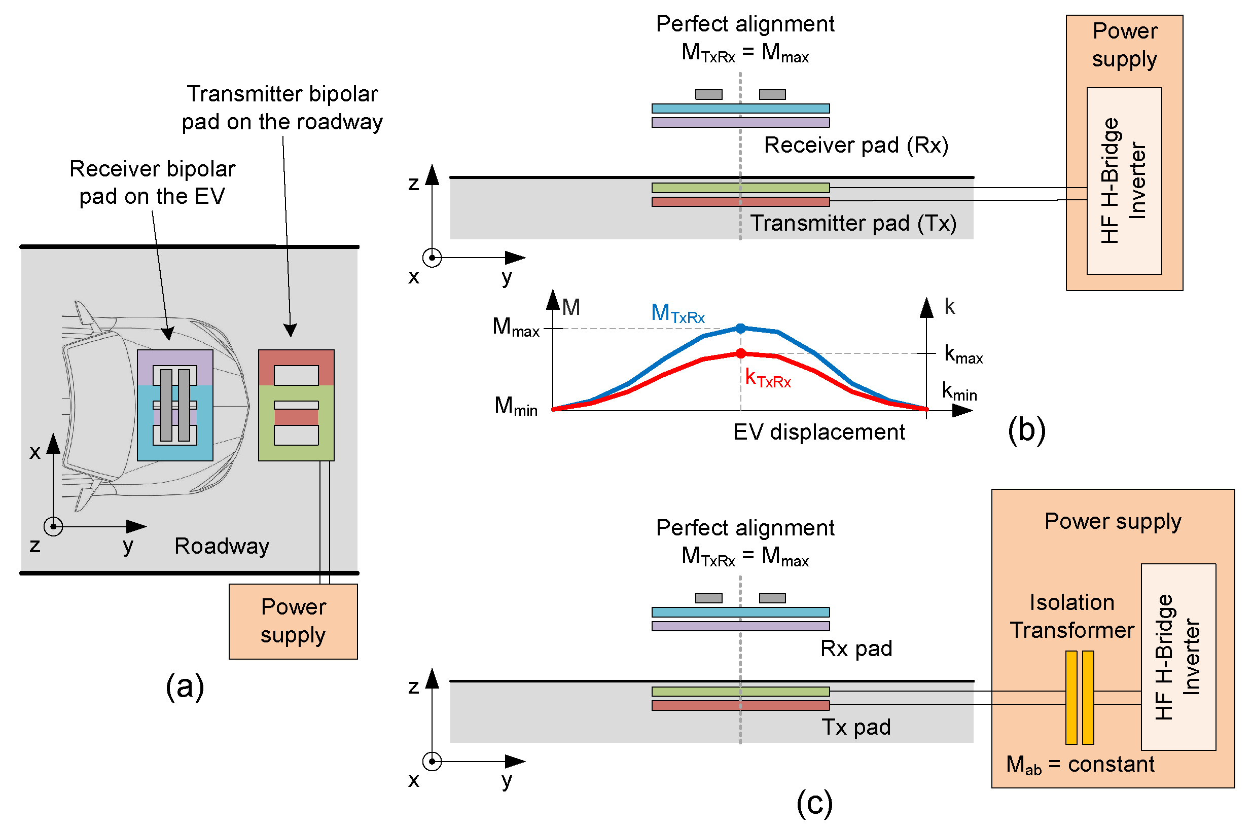
Figure 1. DIPT system pads placement. (a) Typical pads placement on the roadway and onboard of the EV, (b) Single-coupling topology, and (c) Double-coupling topology.
Energies 16 07269 g001
Figure 2. DIPT EV displacement impact.
Energies 16 07269 g002
Figure 3. Typical resonant converter topology with dependent voltage sources model and impedances.
Energies 16 07269 g003
Figure 4. Simulation and experimental results. (a) Mutual inductance and (b) Coupling factor as function of Y misalignment.
Energies 16 07269 g004
Figure 5. Input impedance as function of the mutual inductance: (a) Module and (b) Phase angle.
Energies 16 07269 g005
Figure 6. Voltage and current gains as function of the mutual inductance: (a) Transconductance G i T x v i n and (b) Voltage transfer function G v R v i n .
Energies 16 07269 g006
Figure 7. Equivalent circuit model of a double-coupling SSS configuration in [23]: (a) Coupling mode and (b) No-coupling mode.
Energies 16 07269 g007
Figure 8. Plots of (a) Amplitude of Z i n S S as a function of frequency for different k a b and L a = L b values, and (b) RMS values of odd harmonics in V ¯ i n as a function of α .
Energies 16 07269 g008aEnergies 16 07269 g008b
Figure 9. MATLAB/Simulink simulation model for the double-coupling SSS topology.
Energies 16 07269 g009
Figure 10. Equivalent circuit for variable mutual inductance model simulation implementation.
Energies 16 07269 g010
Figure 11. Simulation results for currents and voltages as function of the time with variable coupling and load step for the classical SS topology (a,c,e) and for the double-coupling SSS topology (b,d,f).
Energies 16 07269 g011
Figure 12. Experimental setup with 1 transmitter and 1 receiver pad with double-coupling SSS topology.
Energies 16 07269 g012
Figure 13. Experimental results with 1 transmitter and 1 receiver pad for double-coupling SSS topology. (a) Full-coupling and full-load, (b) Full-coupling and no-load, (c) No-coupling, (d) Variable coupling and full-load, (e) Variable coupling and no-load, and (f) Variable coupling and load step from full-load to no-load condition. v i n   [ 100   V / div ] CH1 (yellow), i i n = i a   [ 20.0   A / div ] CH2 (blue), v o   [ 20   V / div ] CH3 (pink), and i b = i T x   [ 50   A / div ] CH4 (green). (ac) Time [ 20   μ s / div ] , and (df) Time [ 1   s / div ] .
Energies 16 07269 g013
Table 1. Different battery technology characteristics [1].
TypeEnergy Efficiency [%]Energy
Density [Wh/kg]
Power
Density [W/kg]
Life CyclesSelf-Discharge
Pb-Acid70–8020–3525200–2000Low
Ni-Cd60–9040–60140–180500–2000Low
Ni-MH50–8060–80220<3000High
Li-Ion70–85100–200360500–2000Medium
Li-Polymer70200250–1000>1200Medium
Table 2. Commercial and research groups using IPT technology.
CompanyOutput Power [kW]ApplicationVehicle Type
Witricity11StaticEVs
Brusa11StaticEVs
ENRX100StaticEVs and Buses
ENRX180DynamicBuses
WAVE250StaticBuses
Research Groups and Universities
University of Coimbra/IT1–3Static/DynamicEVs
University of Auckland1–11Static/DynamicEVs
ETH50StaticBuses
ORLN120StaticEVs and Buses
KAIST180DynamicBuses
Table 3. Reflected secondary impedances—Generic and tuned conditions.
GenericTuned Conditions (at b R x = 1 Secondary Side Resonance)
Real Imag Real Imag Observations
Z r e f S ω 2 M T x R x 2 R L R x 2 ω 2 ( 1 b R x 2 1 ) 2 + R 2 ω 3 L R x M T x R x 2 ( 1 b R x 2 1 ) L R x 2 ω 2 ( 1 b R x 2 1 ) 2 + R 2 ω 0 2 M T x R x 2 R 0 - Voltage source characteristics
- Null reflected reactance
- Primary-side compensation
- not affected
Z r e f P ω 2 M T x R x 2 R R 2 ( 1 b R x 2 ) 2 + ω 2 L R x 2 M T x R x 2 ω ( R 2 b R x 2 ( 1 b R x 2 ) ω 2 L R x 2 ) L R x ( R 2 ( 1 b R x 2 ) 2 + ω 2 L R x 2 ) M T x R x 2 R L R x 2 ω 0 M T x R x 2 L R x - Current source characteristics
- Reflected reactance M T x R x
- dependent
- Primary-side compensation
- affected by M T x R x
Table 4. Resonant network input impedances—Generic condition.
RealImagObservations
Z i n S S ω 2 M T x R x 2 R L R x 2 ω 2 ( 1 b R x 2 1 ) 2 + R 2 b T x 2 1 ω C T x + ω 3 L R x M T x R x 2 ( 1 b R x 2 1 ) L R x 2 ω 2 ( 1 b R x 2 1 ) 2 + R 2 - Voltage source characteristics
- No-load/no-coupling: I i n
- Load/coupling: limits I i n at high values
- ϕ Z i n coupling- and load-independent
Z i n S P ω 2 M T x R x 2 R R 2 ( 1 b R x 2 ) 2 + ω 2 L R x 2 b T x 2 1 ω C T x + M T x R x 2 ω ( R 2 b R x 2 ( 1 b R x 2 ) ω 2 L R x 2 ) L R x ( R 2 ( 1 b R x 2 ) 2 + ω 2 L R x 2 ) - Current source characteristics
- Load/No-load: limits I i n
- Coupling/no-Coupling: limits I i n
- ϕ Z i n varies with load and coupling
- ϕ Z i n load-independent at M m a x
Z i n P S 1 j ω C T x ( j ω L T x + Z r e f S ) 1 j ω C T x + j ω L T x + Z r e f S - Needs input choke inductor
- Voltage source characteristics
- No-load/no-coupling: V i n
- Load/coupling: limits V i n
- ϕ Z i n varies with load and coupling
Z i n P P 1 j ω C T x ( j ω L T x + Z r e f P ) 1 j ω C T x + j ω L T x + Z r e f P - Needs input choke inductor
- Current source characteristics
- No-load/no-coupling: V i n
- Load/coupling: limits V i n
- ϕ Z i n varies with load and coupling
Z i n L C L S j ω L i n + 1 j ω C T x ( j ω L T x + Z r e f S ) 1 j ω C T x + j ω L T x + Z r e f S - Additional L i n in the resonant network
- Voltage source characteristics
- No-load/no-coupling: I i n 0
- Load/coupling: limits I i n
- ϕ Z i n coupling- and load-independent
Z i n L C L P j ω L i n + 1 j ω C T x ( j ω L T x + Z r e f P ) 1 j ω C T x + j ω L T x + Z r e f P - Additional L i n in the resonant network
- Current source characteristics
- No-load/no-coupling: limits I i n
- Load/coupling: limits I i n
- ϕ Z i n varies with load and coupling
Table 5. Comparison of the analyzed resonant configurations. Green and red colours refer to pros and cons, respectively, of a topology considering DIPT application and, yellow colour means not suitable for DIPT.
Parameter\TopologySSSPPSPPLCL-SLCL-PSSS
Independence on
L T x R x and R a c
TransmitterYesNoNoNoYesNoYes
ReceiverYesNoYesNoYesNoYes
Zero coupling allowanceNot allowedAllowedNot allowedNot allowedAllowedAllowedAllowed
Total impedanceDecreases with displacementDecreases with displacement but limited to value different from zero.Increases with displacementIncreases with displacementIncreases with displacementIncreases slightly with displacementIncreases with displacement
Load independent output at resonanceVoltage and currentVoltage and currentOnly voltageOnly currentOnly voltageOnly currentVoltage and current
Resonance affected byCouplingNoYesYesYesNoYesNo
LoadNoYes, but load independent at M m a x YesYesNoYesNo
Other advantagesNot suitable for DIPT.(1) Requires a smaller receiver coil self-inductance than SS.
(2) The parallel resonant circuit supplies the stable current.
Not suitable for DIPT.Not suitable for DIPT.Current source characteristics at the transmitter pad input.(1) Galvanic isolation.
(2) Constant intermediate coil current.
Other drawbacksLacking DC component blocking.Additional inductor relatively to classical topologies.Requires additional isolation transformer and resonant capacitor.
Table 6. Simulation and experimental prototype parameters.
ParameterValues
V d c 100 V
f s 20 kHz
P H S 180
M C 1 L a = 41.78 μ H; r a = 0.11 Ω
L b = 42.29 μ H; r b = 0.11 Ω
M a b = 30.27 μ H
k a b = 0.72
M C 2 L T x = 45.7 μ H; r T x = 0.11 Ω
L R x = 57.45 μ H; r R x = 0.11 Ω
M T x R x = [ 0 16.68 μ H]
k T x R x = [ 0 0.33 ]
Resonant capacitors C a = 1.46 μ F
C T x = 783.3  nF
C R x = 1.1 μ F
C o 100 μ F
R o 2.4 Ω
Table 7. Theoretical, simulation, and experimental results, and respective errors.
Theoretical
Results
Simulation
Results
Experimental
Results
Error
Simul. vs. Theor.
Error
Exp. vs. Simul.
Full-coupling and
full-load condition
I i n 16.36 A15.18 A14.58 A7.2%3.9%
I T x 25.43 A22.94 A23.96 A9.8%4.5%
V o 48.33 V47.52 V41.60 V1.7%12.5%
Disclaimer/Publisher’s Note: The statements, opinions and data contained in all publications are solely those of the individual author(s) and contributor(s) and not of MDPI and/or the editor(s). MDPI and/or the editor(s) disclaim responsibility for any injury to people or property resulting from any ideas, methods, instructions or products referred to in the content.