Article

High-Efficiency Sine-Wave Current Pulses Charging Method in Wireless Power-Transfer System Applications

1
Department of Electrical Engineering, National Penghu University of Science and Technology, Magong City 88046, Taiwan
2
Department of Electrical Engineering, Kun Shan University, Tainan City 710303, Taiwan
*
Author to whom correspondence should be addressed.
Energies 2023, 16(20), 7102; https://doi.org/10.3390/en16207102
Submission received: 3 September 2023 / Revised: 5 October 2023 / Accepted: 11 October 2023 / Published: 16 October 2023
(This article belongs to the Section E: Electric Vehicles)

Abstract

:
There has been extensive discourse surrounding energy storage equipment and technologies for sustainable energy solutions. To address the need for prolonging the operational lifespan of energy storage equipment, this research introduces a high-efficiency charging method that integrates wireless power-transfer (WPT) technology. In the proposed LLC-S charger, the diodes of the receiver side rectify the incoming power while generating interleaved sinusoidal wave current pulses for charging two lead-acid battery energy storage systems (BESSs). This approach offers the advantage of providing rest intervals for BESSs and mitigating the impact of electrochemical reactions, thus promoting their overall durability. To validate the proposed charger, two 60 V/14 Ah BESSs as storage equipment within the solar power system are utilized for the charging tests. The results revealed that the utilization of sine-wave current pulses for charging enabled soft switching at both the transmitter and receiver sides, resulting in an overall average efficiency exceeding 80%. Experimental data derived from a prototype with a maximum output power of 1391 W during charging demonstrated that BESSs could be fully charged in a mere 1.61 h, achieving an impressive efficiency of 98%. These findings substantiate the feasibility and effectiveness of utilizing sine-wave current pulses for charging.

1. Introduction

Wireless power transfer is a safe charging method that has been extensively used for charging electric vehicles, mobile phones, biomedical implants, and other devices. Wireless transmitters can transmit green energy through the air to receivers that are located at distances ranging between 0 and 100 cm. Although wireless power transfer was first demonstrated by Nikola Tesla through the invention of the Tesla coil [1], notable breakthroughs in WPT technology were not achieved until the early 21st century. In 2007, a research team at the Massachusetts Institute of Technology (MIT) proposed strongly coupled magnetic resonance for WPT [2] as a replacement for the traditional inductive power-transfer method, which has low efficiency and coupling. Magnetic resonance-based wireless charging technology [3] was first developed in 2008 when researchers at an MIT laboratory lit a 60 W light bulb using a wireless power-transfer system; the efficiency of their system was estimated to be 15%. To improve the conversion efficiency of wireless power systems, several experts have attempted to optimize the circuit structure, cost, and efficiency of such systems. For example, Noeren et al. [4] and Tran et al. [5] have developed wireless chargers with maximum conversion efficiencies of 92.0% and 97.08%, respectively. Although the charger developed by Tran et al. has a relatively high conversion efficiency, it is composed of four coils resulting in an excessively complex circuit structure and excessively high circuit cost. Ramezani et al. [6] developed a wireless charger with a conversion efficiency of 94.8%; nevertheless, this charger comprises an LCC-series compensation circuit, resulting in a complex and costly structure. Furthermore, Park et al. [7] presented a wireless charger with a maximum conversion efficiency of 92.7% in the WPC/PMA mode, and Yoo et al. [8] presented a half-bridge LLC resonant converter with a conversion efficiency of 93%. Corti et al. [9] also proposed a wireless charger with a conversion efficiency of 90.0%, and Nama et al. [10] designed a wireless charger with a conversion efficiency of 91.26%. Additionally, Li et al. [11] developed a double-sided LCC wireless charger with a maximum conversion efficiency of 96%.
On the basis of the preceding literature review, the present study developed a wireless charger with a low circuit cost, high circuit efficiency, and simple circuit structure for achieving high-efficiency wireless charging through the use of green energy; the charger applies an interleaved method to deliver power in the form of sine waves. Figure 1 illustrates the circuit diagram of the proposed wireless charger. This circuit contains an inverter, a resonance tank consisting of an LLC-S compensation network, and a rectifier circuit. This research employs magnetic resonance for the achievement of wireless power transmission. The technology can be described as follows: In Figure 1, the DC power input undergoes switching through four active switches in the full-bridge inverter, resulting in the generation of a high-frequency square-wave AC voltage. This AC voltage is then directed to the LLC compensation network. Utilizing the fundamental harmonic approximation (FHA), the square-wave AC voltage can be represented as an AC signal through the Fourier series equation. Subsequently, the signal is amplified by the LLC compensation network to produce the AC power supply for the transmitting coil. The relationship between the transmitting coil and the receiving coil is based on coupled inductance application, with the mutual inductance contingent upon factors such as air-gap distance, the number of coils, and the diameters encompassed by the coils. The amplified AC power effectively transfers power from the input to the receiver side across the air gap, with both the receiver and transmitting sides resonating at the same frequency; that is, the magnetic resonance method. On the receiver side, a coil and a capacitor combination form a series resonance circuit. The primary function of the receiver side is to receive the AC power transmitted from the transmitting coil and subsequently supply DC power to the load through output rectifier diodes. In general, a conventional LLC-S compensation resonant circuit contains a leakage inductor and a self-inductor. By contrast, the LLC-S resonance compensation circuit used in the proposed charger contains an additional winding of a small and independent air-core inductor t instead of a leakage inductor to reduce system cost and weight and increase design freedom. For enhanced conversion efficiency, in a study referenced as [11], simulations were conducted for both the S–S (Series–Series) and LCC (LCC resonant) compensation systems with elevated mutual inductance values. The findings indicate that the SS compensation topology exhibits superior efficiency. Notably, the LLC structure, a variant of SS compensation, offers increased controllability. As a result, it has been chosen as the preferred configuration for the present research. In addition, because of the innate function of the LLC resonance compensation network, the four active switches on the transmitter side can achieve zero-voltage switching (ZVS), and the diode on the receiver side can approximately achieve ZVS and zero-current switching (ZCS), which improves the conversion efficiency during charging. This study conducted experiments to verify the performance of the proposed wireless charger. The proposed charger completed the charging of two lead-acid BESSs in 2.0 h, achieved a maximum output power of 1391 W, and exhibited a maximum efficiency of 98%.
The remarkable features of this research encompass its significant contributions to the following aspects:
  • In contrast to the square-wave pulse-charging method, this research demonstrates that the electrochemical reaction rate of the battery can catch up with the charging current. This novel charging method serves as an indirect safeguard for the battery, effectively prolonging its cycle life;
  • Introducing interleaved charging technology allows for the simultaneous charging of multiple batteries, addressing the limitations of traditional single-output charging methods;
  • The charger incorporates a small independent air-core inductor, eliminating the issue of difficult-to-control leakage inductance. This enhancement enhances design flexibility and enables the realization of the LLC-S charger;
  • Compared to conventional LLC converters, the receiver side of the circuit features a reduced number of components, while soft switching technology further enhances the overall circuit efficiency. This results in a simple, cost-effective, and easily maintainable circuit, well-suited for high-power battery-charging applications;
  • This research offers a comprehensive design process along with equipment brands and models, simplifying the replication and implementation of the proposed wireless circuit.
The rest of this paper is organized as follows. Section 2 describes the operating principle of the charger’s circuit. Section 3 describes the characteristics of the proposed charger and its charging method considerations. Section 4 details the design procedure for the proposed charger. Section 5 presents the experimental results, including the measured waveforms, charging time, and efficiency of the prototype. Section 6 provides the study conclusion.

2. Operational Principle

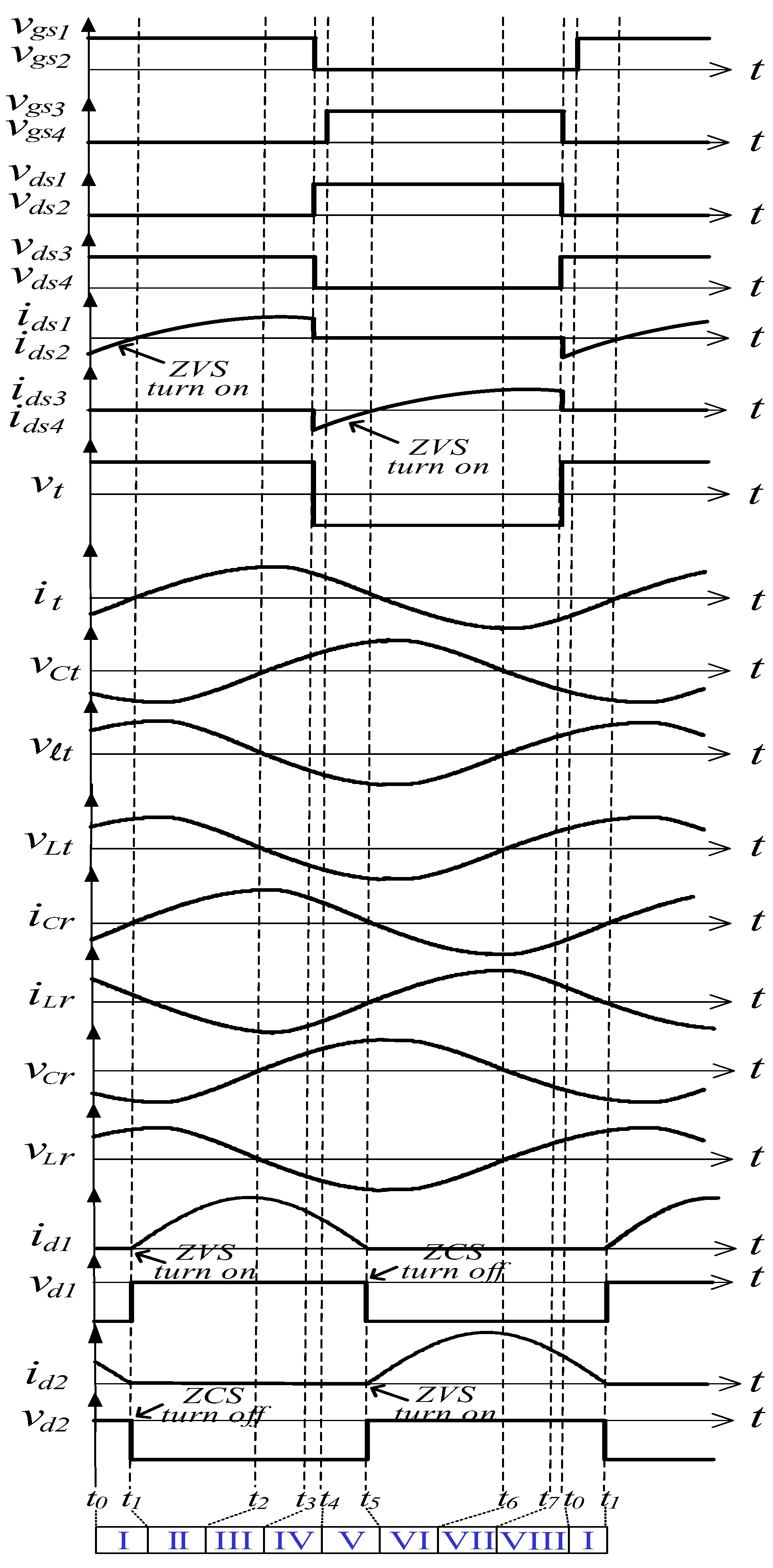
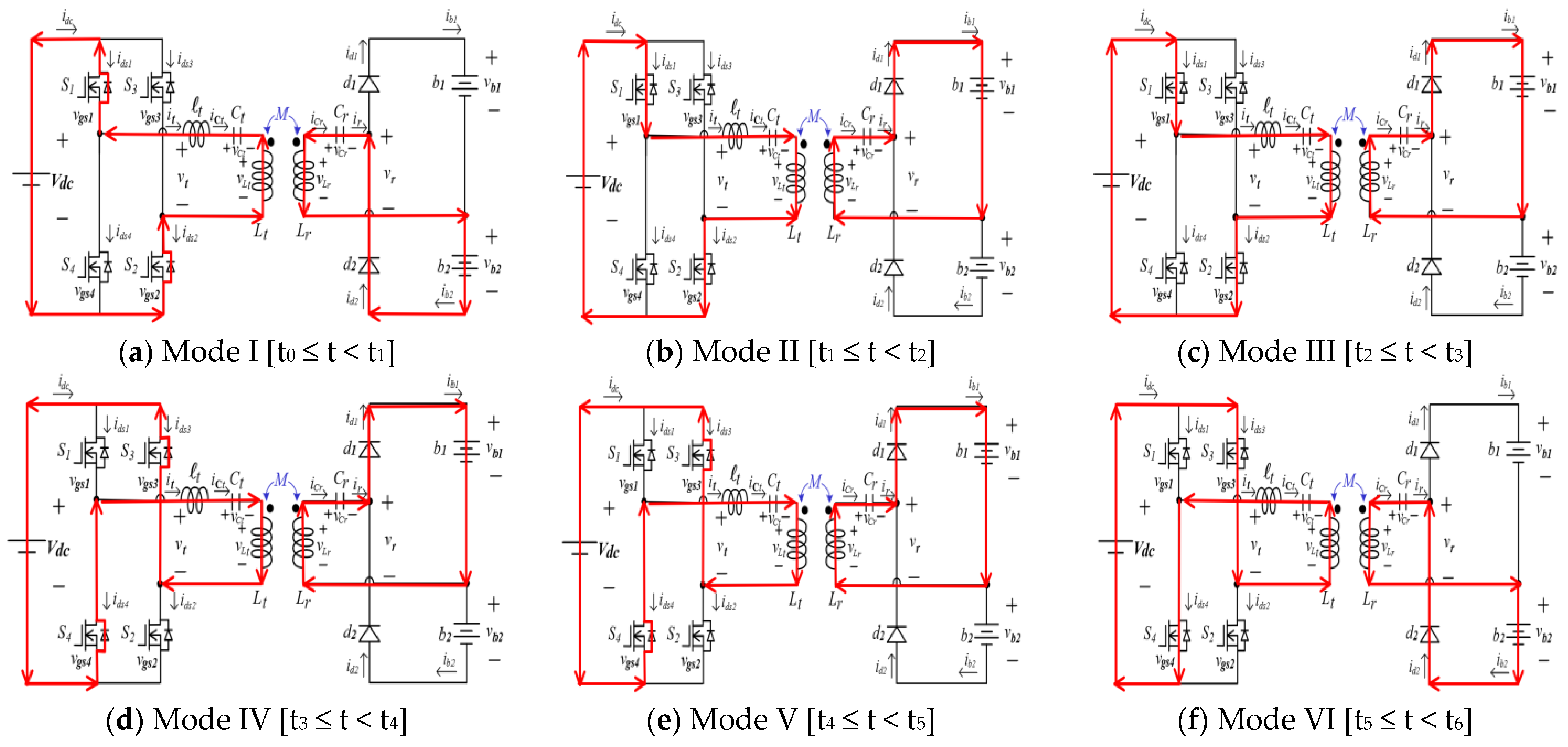
Figure 1 displays the circuit structure of the proposed sine-wave current pulses wireless charger. This charger contains four power transistors (S1–S4) that form the inverter on the transmitter side, an LLC-S resonance compensation network, and interleaved output circuits composed of a half-bridge rectifier. Figure 2 illustrates the timing diagram of the proposed circuit. This circuit involves eight operating modes, as marked I~VIII at the bottom of Figure 2, the working interval is shown by the dotted line, and each of which is described as follows.
(1)
Mode I [Figure 3a, t0t < t1]: At t0, the resonant current it flows through the parasitic diodes of switches S1 and S2; therefore, the voltage of these switches can be reduced to 0 V to enable the switches to achieve ZVS in the next turn-on period. On the receiver side, the battery bank of b2 is in the charging state. The equivalent circuit for mode I operation is displayed in Figure 3a;
(2)
Mode II [Figure 3b, t1t < t2]: Between t1 and t2, the current idc flows forward to switches S1 and S2; thus, these switches are turned on under the ZVS manner. In the resonance compensation network, the resonant inductor t, the transmitting coil Lt, and the capacitor Ct are in resonance. Moreover, the current iCr charges the battery bank of b1. The equivalent circuit for mode II operation is in Figure 3b;
(3)
Mode III [Figure 3c, t2t < t3]: Switches S1 and S2 remain turned on until t3 is reached. The resonant current reaches its maximum value at t2; therefore, the voltages of the inductor t, Lt, and capacitor Ct begin to reverse in the resonance compensation network, and the voltage polarity across inductor Lr and capacitor Cr changes. The battery bank of b1 is continuously charging during mode III, and the equivalent circuit for mode III operation is shown in Figure 3c;
(4)
Mode IV [Figure 3d, t3t < t4]: Between t3 and t4, all switches(S1–S4) are in the off state because of the deadtime process. Because the resonant current it flows in a freewheeling state through switches S3 and S4, the voltages vds3 and vds4 can be quickly reduced to 0 V to enable ZVS operation. Moreover, the resonance-tank voltage vt reverses polarity at t3. On the receiver side, current iCr continues to charge the battery bank of b1. The equivalent circuit for mode IV operation is shown in Figure 3d;
(5)
Mode V [Figure 3e, t4t < t5]: Between t4 and t5, switches S3 and S4 are in a zero-voltage state because the resonant current it flows in a freewheeling state. The battery bank of b1 is charged continuously during mode V operation, and the equivalent circuit of mode V operation is illustrated in Figure 3e;
(6)
Mode VI [Figure 3f, t5t < t6]: At t5, the current it begins to commutate, and switches S3 and S4 are turned on under ZVS. On the receiver side, currents iCr and iLr also begin to, and rectifier diode d2 is turned on under ZVS; therefore, battery b2 begins charging. The equivalent circuit of mode VI operation is shown in Figure 3f;
(7)
Mode VII [Figure 3g, t6t < t7]: Switches S3 and S4 are continuously turned on. At t6, multiple voltages, including the capacitor voltages vCt, and vCr, inductor voltage vt, and coil voltages vLt and vLr, are set to 0 V. Moreover, the currents, including the resonant current it, capacitor current iCr, and inductor current iLr, are in a peak value state. The battery bank of b2 continues to be charged until t7. The equivalent circuit of mode VII operation is displayed in Figure 3g;
(8)
Mode VIII [Figure 3h, t7t < t0]: Between t7 and t0, switches S1–S4 are again switched off because of the deadtime process. The resonant current it flows through the parasitic diodes of switches S1 and S2, which forces the voltages vds1 and vds2 to decrease to 0 V; thus, a ZVS state is created in the next turn-on period. Furthermore, the polarity of the resonant tank voltage vt changes again. The resonant current ir on the receiver side still charges the battery bank of b2 to complete a cycle of interleaved charging. The equivalent circuit for mode VIII is presented in Figure 3h.

3. Circuit Characteristics and Charging Method Considerations

3.1. LLC-Converter Characteristics

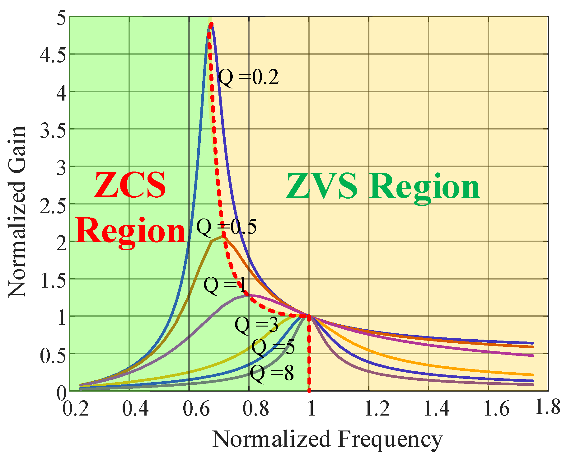
The LLC converter has been widely used because of its high power density and high efficiency; thus, it is adopted for the proposed charging method. The characteristics of an LLC circuit are illustrated in Figure 4. The figure shows six curves of quality factor Q from 0.2 to 8, in which the y-axis represents the normalized gain of the converter, the x-axis represents the normalized frequency, and the red dotted line represents the dividing line between ZCS and ZVS. Following the peak value of each curve, a zero-current switching zone and a zero-voltage switching zone can be constructed. The figure shows that the smaller the quality factor Q has, the higher the normalized gain, which shows that the larger the load RL value (light load) under the constant characteristic impedance, the higher the voltage gain. That is, the smaller quality factor can occur; on the contrary, the higher quality factor can occur at heavy load conditions. In order to reduce the high circulating current on the transmitting side, the ratio of these two parameters, Lt and t, can usually be adjusted. When the inductance Lt is larger, a relatively small circulating current can be obtained, which can effectively reduce the current loss and heating of the transmitting-side devices, thereby improving the overall efficiency. Based on the above description and corresponding to the curve in Figure 4, a larger inductance Lt can be mapped as a quality factor curve with a high Q value.
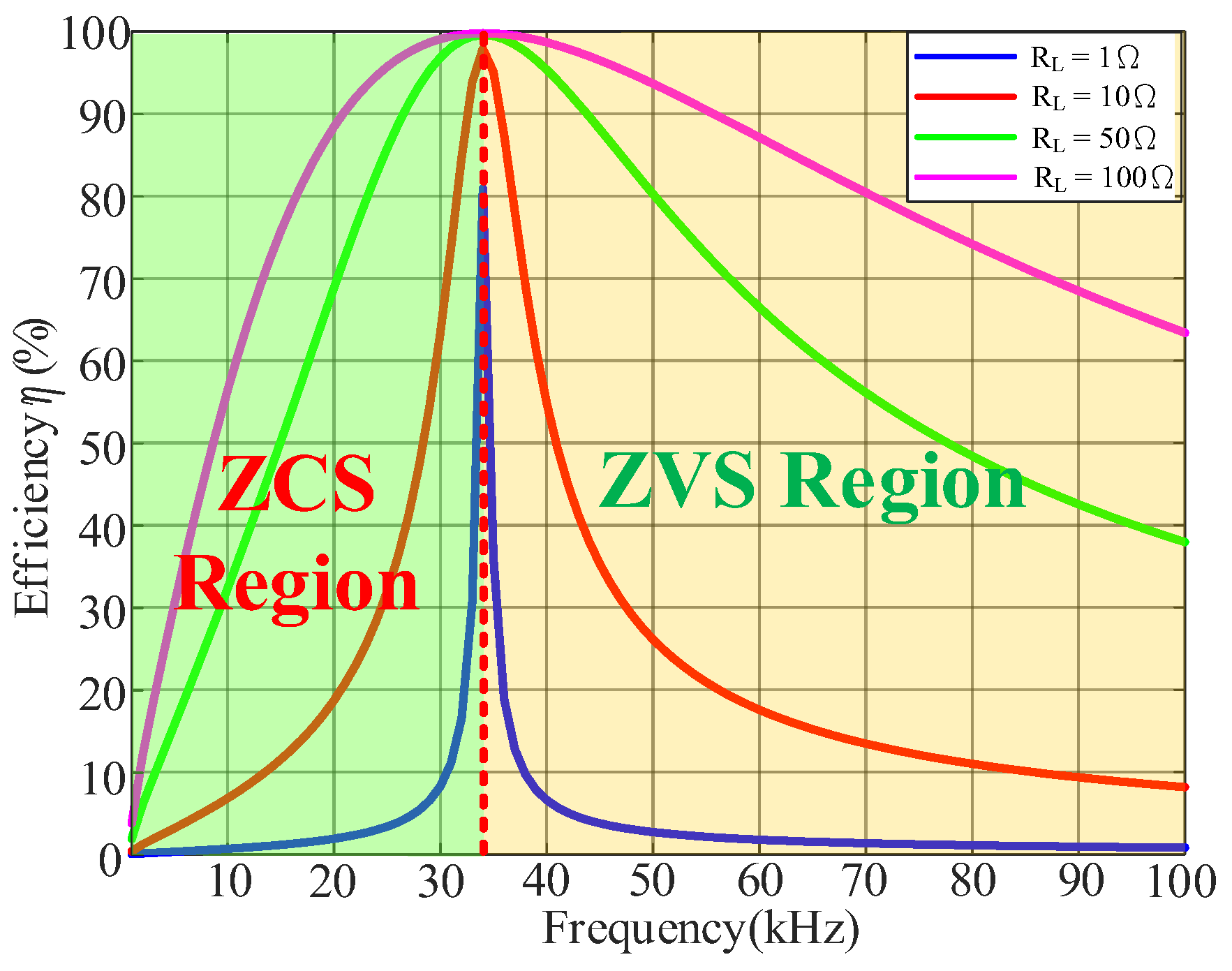
To further analyze the efficiency of the LLC converter under different loads, the simulation results are shown in Figure 5. The figure shows four curves from 1 to 100 Ω different loads, where the y-axis represents the conversion efficiency of the converter, the x-axis represents the operating frequency fs, and the red dotted line represents the dividing line between ZCS and ZVS. From the curve of 1 Ω load, it can be seen that operating at the resonant frequency has a maximum conversion efficiency of 81%; it also shows that this curve has the smallest bandwidth, which is not conducive to the stability of the system. For the curve of 10 Ω load, both conversion efficiency and bandwidth are developing towards a better trend, and it has a maximum conversion efficiency of 97.87%. When the load is equal to 100 Ω, the maximum conversion efficiency can reach 100%. Moreover, it has the widest bandwidth among these curves.
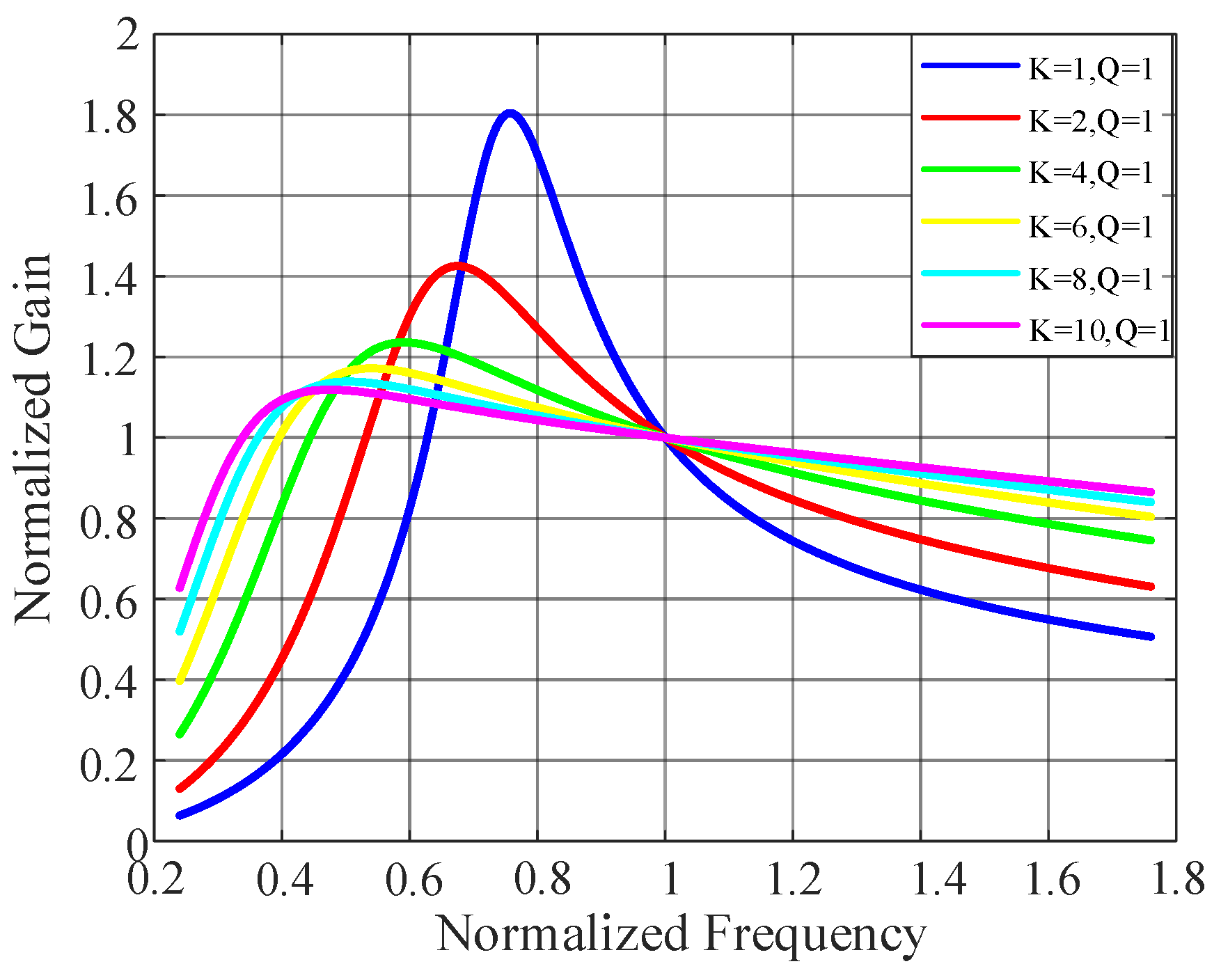
In order to further understand the relationship between the transmitting coil inductance Lt and the air inductance t (K = Lt/t) in the LLC-S system, the simulation results of fixed quality factor Q and the inductance ratio K under normalized frequency are shown in Figure 6. It can be seen from the figure that a small K value has a high voltage gain, which means that the circulating current at the transmitter side is also larger. Conversely, a larger K value can obtain a smaller circulating current on the transmitter side. For general LLC converters, the K value ranges from about 5~10.

3.2. Equivalent AC Circuit Analysis

The conventional S–S resonant circuit is applied in the WPT system [12,13]. The compensation capacitor at the transmitter side is independent of the load, and it is suitable for charging the battery. In the meantime, its output provides a constant current characteristic, which is a natural advantage for battery charging. The S–S compensation system achieves high and stable transmission efficiency at low mutual inductance. Furthermore, it delivers the highest output power at a fixed input power compared to other systems. However, the disadvantage of this second-order series resonant circuit is that the DC gain is always less than one, which means that can only be limited to step-down operation. The LLC circuit structure belongs to the series resonant converter (SRC), which is realized by adding an additional inductor to the original second-order series resonant circuit. Relatively, the LLC converter can perform both step-up and step-down functions, which improves the disadvantage that the second-order series resonant circuit can only operate at step-down mode, simultaneously, the converter has a wide output power control range and can also realize zero voltage switching. Therefore, the LLC converter with high efficiency is applied to the transmitting side of the WPT system, and the LC converter with a step-down function is applied to the receiving side, which is to form the LLC-S wireless charger proposed in this study.
Figure 7 illustrates the equivalent AC circuit of the proposed LLC-S wireless charger, and the pink dotted line in the figure represents the mutual inductance coupling model. The resonant current it flows through the transmitting coil Lt and generates a time-variant magnetic field around the coil. Moreover, the receiving coil Lr cuts off the magnetic field to induce a voltage. The magnitude of the induced voltage depends on the air gap between the transmitting and receiving coils, the coil lengths, the number of coil turns, and the derivative of the magnetic field with respect to time. Because an air gap exists between the transmitting coil Lt and receiving coil Lr, the mutual inductance M generated by the two coils affects their voltages, in addition to affecting the power and conversion efficiency of the system.
On the basis of Kirchhoff’s voltage law (KVL), the following equations can be derived for the circuit presented in Figure 7.
Z 1 i t j ω M i r = v t j ω M i t + Z 2 i r = 0
where Z1 is the equivalent impedance of the transmitter side, Z2 is the equivalent impedance of the receiver side, and Zr in Figure 7 is the same as Z2, which is the equivalent impedance of the receiver side. The impedances Z1 and Z2 can be expressed as Equation (2).
Z 1 = R L t + j ω t + R t + 1 j ω C t + j ω L t Z 2 = j ω L r + R L r + 1 j ω C r + R L
According to Equation (1), the resonant current it on the transmitter side and the resonant current ir on the receiver side can be expressed as follows:
i t = Z 2 v t Z 1 Z 2 + ( ω M ) 2 i r = j ω M v t Z 1 Z 2 + ( ω M ) 2
When the proposed wireless charger operates at resonance, the capacitive reactance and inductive reactance are identical in magnitude but opposite in polarity, as expressed in Equation (4):
j ω t + 1 j ω C t + j ω L t = 0 j ω L r + 1 j ω C r = 0
Equations (2) and (4) can be rearranged, as follows:
Z 1 = R L t + R t Z 2 = R L r + R L
According to the equivalent dependent power source (−j ω Mir) of the transmitter, the equivalent impedance reflected from the receiver side to the transmitter side can be shown as follows:
Z r = ( ω M ) 2 Z r
where the apostrophe ‘‘ ’’ indicates the variables of the receiver side that correspond to those of the transmitter side.
The total impedance of the overall circuit can be derived as follows:
Z t = ( R L t + j ω t + R t + 1 j ω C t + j ω L t ) + ( ω M ) 2 ( j ω L r + R L r + 1 j ω C r + R L )
On the basis of the preceding equation, the input power Pi and the output power Po can be expressed as follows:
P i = v t i t = v t 2 ( R L r + R L ) ( R L t + R t ) ( R L r + R L ) + ( ω M ) 2 P o = i r 2 R L = v t 2 ( ω M ) 2 R L [ ( R L t + R t ) ( R L r + R L ) + ( ω M ) 2 ] 2
Therefore, the conversion efficiency of the proposed charger can be derived as follows:
η = ( ω M ) 2 R L [ ( R L t + R t ) ( R L r + R L ) + ( ω M ) 2 ] ( R L r + R L ) × 100 %
The sinusoidal current generated by the resonant circuit originates from the high-frequency square wave switched by switches S1–S4; however, the resonant circuit allows only the power of the fundamental component to pass through. According to FHA, the fundamental frequency of the Fourier series of voltage can be expressed as follows:
v r t = n = 1 , 3 , 5 4 v b 1 n π sin ( n ω t )
The fundamental component of the voltage vr1 can be derived as follows:
v r 1 = 4 v b 1 π sin ( ω t )
where vr is the output voltage of the AC-equivalent model in Figure 7, vb1 is the battery-bank voltage of b1, n is the number of harmonics, and ω is the angular frequency.
The power of the receiving coil is rectified by a half-bridge circuit and converted into the charging battery voltage vb1 and current ib1. Thus, the average value of the charging current ib1 can be derived as follows:
i b 1 , a v g = 1 2 π 0 π i b 1 m sin ω t d ω t = i b 1 m π
The maximum value of the charging current ib1 can be expressed as follows:
i b 1 m = π i b 1 , a v g
The equivalent AC impedance Re can be expressed as follows:
R e = v r 1 m i b 1 m = 4 v b 1 π π i b 1 , a v g = 4 π 2 v b 1 i b 1 , a v g = 4 π 2   R L
where RL is the impedance presented by the battery during charging, including ohmic internal resistance and polarization internal resistance. The impedance RL will change with the charging time, and it is proportional to the equivalent AC impedance Re.

3.3. Considerations Regarding the Charging Methods

In addition to the charging efficiency of the converter, another issue that needs attention is the battery-charging methods. Lead-acid batteries are widely used in the energy storage equipment [14,15,16,17,18] of renewable energy and microgrid systems because of their low cost and safety. In general, five charging methods exist for batteries: constant-voltage (CV) charging, constant-current (CC) charging, constant-current–constant-voltage (CC–CV) hybrid-charging, pulse-charging, and reflective-charging methods [19,20,21,22,23,24,25]. To achieve fast charging, the CC charging method is usually used; however, other charging methods are more suitable for certain types of batteries. For example, the CC–CV hybrid charging method is suitable for lithium batteries, whereas the pulse-charging or reflective-charging methods are suitable for lead-acid batteries. Additionally, it is crucial to closely monitor battery temperature fluctuations during the charging process, particularly in rapid charging scenarios. Stringent temperature-control standards apply when charging lead-acid batteries, with a recommended upper limit of 45 °C. This limitation is primarily attributed to the chemical reactions occurring within the battery. Specifically, during these reactions, the positive plate generates lead dioxide, while the negative plate produces velvety lead. Elevated temperatures can lead to the formation of coarse particles in these substances, resulting in reduced binding forces and an increased risk of active material detachment from the plates. Such detachment can potentially lead to a short circuit between the battery plates. In [26], at a pulse frequency of 1 Hz, the pulse-charging method was determined to be the most effective approach to battery charging; moreover, the current pulse was noted to increase the Faradaic efficiency of the battery. That is, it reduces the water decomposition rate, and the pulse current does not change the electrochemical steps in the oxygen evolution mechanism. An increase in the current-pulse amplitude can engender a considerable increase in the average double-layer current, which can result in rapid charging. However, in the pulse-charging method, a battery pack is charged using a rectangular current pulse, and a short rest time is provided to reduce the intensity of the electrochemical reaction of the battery. If a high rectangular current pulse is used to charge the battery pack in the aforementioned method, the charging time can be reduced, thus resulting in fast charging. However, in theory, the slope of such current can be expressed as follows:
d i ( t ) / d t =
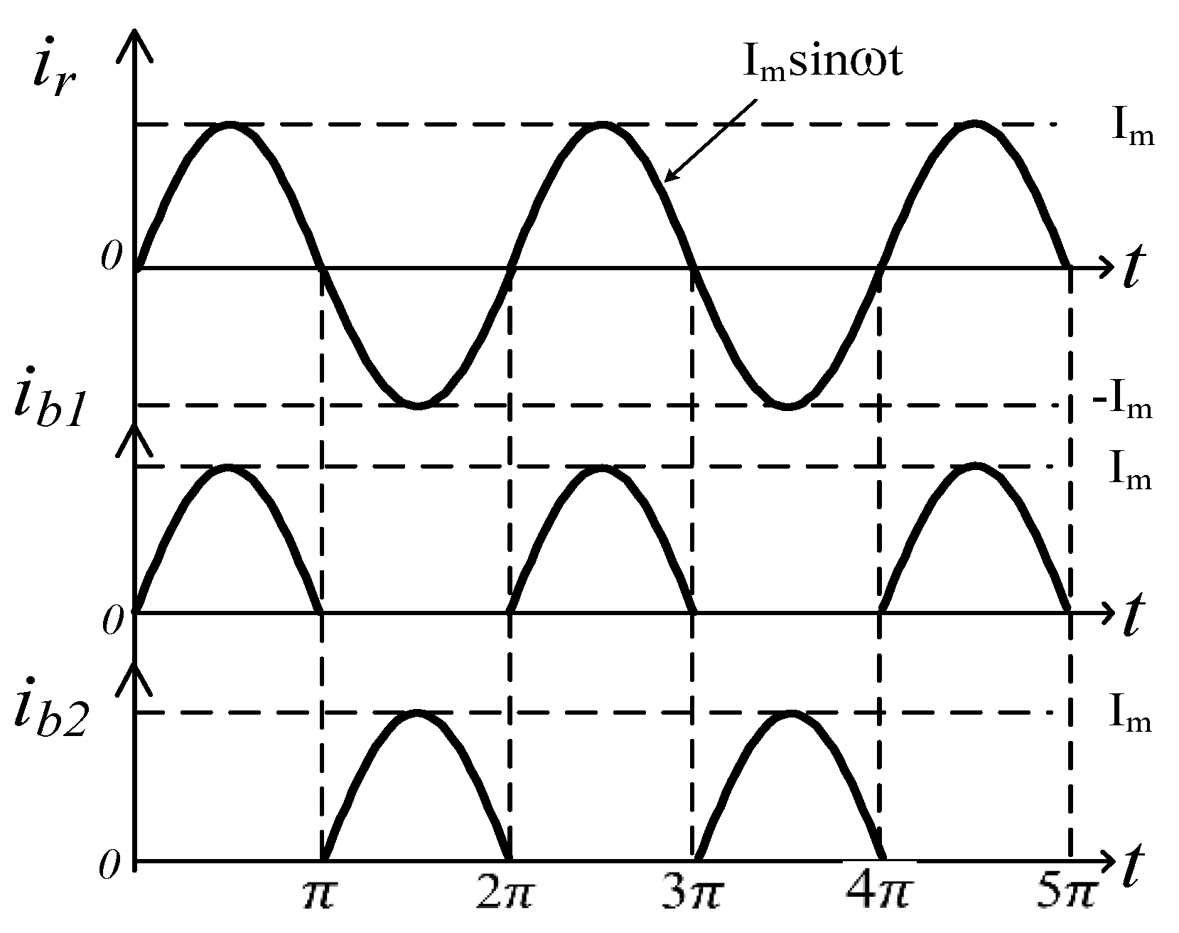
In the conventional pulse-charging method, the current pulse varies infinitely with time; consequently, the electrochemical reaction of the battery may not be able to match the rapidly changing speed of the charging current. To address this limitation, this study developed a wireless charger that can generate interleaved high-frequency, sine-wave current pulses for enhancing lead-acid BESSs, and the schematic diagram of the waveform is shown in Figure 8. In this circuit, the receiving coil of the LLC-S resonance compensation network generates a high-frequency sinusoidal current ir. This current flows through an interleaved rectifier, which can generate two interleaved high-frequency sinusoidal current pulses, namely ib1 and ib2, with a phase difference of 180 ° . With the circuit diagram of Figure 1 and the operational diagram of Figure 8, when the current ib1 charges the battery bank of b1, the charging current of the battery bank of b2 is 0 A; that is, the battery bank of b2 is in a resting state. However, when the current ib2 charges the battery bank of b2, the charging current of the battery bank of b1 is 0 A; that is, the battery bank of b1 is in a resting state. Thus, the two BESSs, namely b1 and b2, operate in an interleaved charging mode. This mode allows the batteries to be charged with a high current to achieve fast charging. Moreover, the interleaved charging mode includes a half-cycle rest time, which enables the electrochemical reaction of the batteries to be slowed down, and their cycle life to be effectively extended. Therefore, the proposed high-efficiency wireless charger provides high-frequency sinusoidal current pulses, which can be expressed as follows:
d i r ( t ) / d t = ω I m s i n ω t
Equation (16) indicates that the high-frequency sinusoidal current pulses of the proposed charger do not vary infinitely with time; instead, these pulses are a function of the circuit resonance frequency ω and peak current Im. Therefore, if the circuit parameters of the proposed charger are appropriately designed, the proposed charger can effectively moderate the internal electrochemical reaction of the battery to extend its cycle life.
Table 1 compares the advantages and disadvantages of the half-bridge charging structure and conventional full-bridge rectifier. The table shows the number of components, battery rest time and cost, etc., indicating that the benefits of using the half-bridge charging structure are more than the full-bridge one.

4. Design Procedure

To ensure the appropriate operation of the proposed wireless charger, the parameters of its resonance compensation network must be suitably designed. However, the LLC resonance compensation network of the proposed charger is composed of three components, and the circuit design is more complicated than that of the second-order one. Hence, the parameters of the resonance compensation network must be designed through a comprehensive procedure, conducted in a strict sequence. The steps involved in the design of a novel high-efficiency sine-wave current pulses wireless charger system with a 20 cm air gap are detailed in the following sections.

4.1. Design of the Resonance Compensation Network

Figure 9 presents the design flow chart of the proposed charger. The design procedure involves determining the charging voltages vb1 and vb2 and the currents ib1 and ib2 according to the capacity and performance of the BESSs; selecting the resonance frequency fm; and determining the capacitance of capacitor Ct, the inductance ratio K value, the number of transmitting coil turns N1, the parameters of the resonant inductor t of the compensation network of the transmitter side, the capacitance of capacitor Cr, and the number of receiving coil turns N2.
The angular frequency ω m at which the transmitter and receiver at resonance can be expressed as follows:
ω m = 1 L t + t C t = 1 L r C r
According to Equation (17), the capacitances of the compensation capacitors on the transmitter and receiver sides can be derived as follows:
C t = 1 ( 2 π f m ) 2 ( L t + t )
And
C r = 1 ( 2 π f m ) 2 L r
where fm is the resonance frequency. It is worth noting that although the three components of LLC are connected in series, even if the capacitance Ct is increased, the same effect as that of increasing inductance t can be achieved by Equation (17). However, inductors and capacitors produce different impedances under various frequencies, which will directly affect the characteristic impedance and quality factor of the WPT system and, ultimately, change the characteristics of the entire system. Therefore, increasing the capacitance Ct cannot achieve the same effect as increasing inductance t.
In this study, planar circular coils were selected as the transmitter and receiver for power transfer. The power-transmission efficiency can be increased by appropriately setting the mutual inductance M between the coils, the self-inductance L of the coils, and the angular frequency of the coils ω. The WPT coil used in this study was equivalent to a coaxial parallel air-core coil, as shown in Figure 10. The mutual inductance M between the transmitting and receiving coils can be expressed as follows [27]:
M = μ 0 × π × N 1 × N 2 × r 1 2 × r 2 2 2 × r 1 2 + d 2 3 2
where μ 0 is the air permeability coefficient, Lt is the inductance of the transmitting coil, Lr is the inductance of the receiving coil, r1 is the outer diameter of the transmitting coil, r2 is the outer diameter of the receiving coil, d is the distance between the transmitting and receiving coils, and N1 and N2 are the numbers of transmitting and receiving coil turns, respectively.
The self-inductance of a coil can be expressed as follows:
L t = N 1 ϕ 1 i t
For a uniform magnetic field, according to Equations (20) and (21), the self-inductance of the transmitting coil can be expressed as follows:
L t = μ 0 × π × N 1 2 × r 1 2
The self-inductance of the receiving coil can be expressed as follows:
L r = μ 0 × π × N 2 2 × r 2 2
In the design procedure of the transmitting coil, the main parameters to be maximized were the coil quality factor Q and coupling coefficient k. In conventional coil design, the value of k is set between 0.3 and 0.5 to fix the coil inductances Lt and Lr. In a wireless transformer, the maximum possible value of k is 0.5. When the coil inductances Lt, coil Lr, and the mutual inductance M are known, the coupling coefficient k can be determined as follows:
k = M L t L r
The quality factors Q can be expressed as follows:
Q = L r / C r R e
According to the design flow chart displayed in Figure 9 and Equations (17)–(25), the voltage and current of the two BESSs must first be determined. Five 12 V lead-acid batteries were connected in series to form a battery group, and two battery groups were created. Considering that the 1 C charging current of the lead-acid battery used is 14 A, the charging current is set to be 8.5 A. Next, considering that an increase in the switching frequency increases the voltage induced in the receiving coil, the conduction loss, Joule loss in the coil, and core loss were increased. Therefore, the resonant frequency fm is set to 34 kHz. The capacitance of capacitor Ct was set to 0.05 μF [27,28,29,30,31,32]. The inductance ratio K value is set to 10; but, for actual adjustment, the optimal parameter approximately equals 11. The air gap between the transmitter and receiver sides was determined to be 20 cm. The number of transmitting coil turns N1 was set to 25, and the outer diameter r1 of this coil was set to 0.31 m. The transmitter inductance calculated using Equation (22) was 382.44 μH; however, the measured transmitter inductance was 400.4 μH. In order to make the switches S1–S4 operate under ZVS condition, the operating frequency fs must be higher than the resonant frequency. According to the literature [33,34,35], the optimal design frequency range is around 1.05~1.2 times the resonant frequency. In this study, the resonant frequency of 1.1 times is determined to be the operating frequency of the system, which is 37.4 kHz, which is actually 37.9 kHz after adjustment. Subsequently, on the basis of Equation (17), the inductance t of the transmitter side was determined to be 37 μH. Similarly, at the same resonance frequency 34 kHz, the capacitance of capacitor Cr was set to 0.1 μF [27,28,29,30,31,32]. The number of receiving coil N2 was set to 18, and the outer diameter r2 of this coil was set to 0.28 m. The receiver inductance calculated using Equation (23) was 179.07 μH; however, the measured receiver inductance was 219.1 μH. Furthermore, the mutual inductance M between the coils was calculated to be 133.15 μH by using Equation (20), and the coupling coefficient k was determined to be 0.45 by using Equation (24).

4.2. Design of the Resonance Compensation Network

This study attempted to design a high-efficiency wireless charger with a rated power of 1500 W and a switching frequency of 37.9 kHz. The transmitting coil of the proposed charger transmits power mainly through the magnetic field generated by the current flowing through it. Power is transferred from the transmitting coil to the receiving coil over an air gap of 20 cm to supply the load. According to the characteristics of the full-bridge circuit, the sustained voltages of switches S1–S4 must be higher than the input voltage Vdc. The sustained current of each switch is expressed in Equation (26). Considering the conduction losses of the circuit components, the IXTK120N65X2 power semiconductor field-effect transistor model was adopted in this study. This model has an on resistance of RDS(on) of ≤23 mΩ and enables the maximum sustained voltage and current to reach 650 V and 120 A, respectively.
i D S > v t Z t c
where vt is the maximum resonant voltage of the transmitter side, and Ztc is the characteristic impedance of the compensation network on the transmitter side.

4.3. Rectifier Diodes

To analyze the voltages across the rectifier diodes of the proposed circuit, the following assumptions can be made: the battery bank of b1 can be assumed to have stopped charging, and the battery bank of b2 can be assumed to be charging. If the forward conduction voltage VF of the diode d1 is ignored, the maximum voltage of the diode d1 should be sustained as:
vd1 = vb1 + vb2
According to Equation (27), d1 must withstand the combined voltage of the battery banks of b1 and b2. However, when the battery bank of b2 is charging, the sum of the voltages vLr and vCr must be higher than the battery voltage vb2; thus, the voltage flowing across diode d1 can be expressed as follows:
vd1 = vCr + vLr + vb1
Combining Equations (27) and (28) yields the following equation:
vb2 < vLr + vCr
The peak diode current of the half-bridge rectifier can be shown in Equation (13). In this study, the breakdown voltage and peak current of the rectifier were determined, and the IQBD60E60A1 ultra-fast diode was selected to meet the requirements of the half-bridge rectifier. This diode can sustain a voltage and current of 600 V and 60 A, respectively, at a forward conduction voltage of 1.3 V. The reverse recovery time of the aforementioned diode ranges from 40 to 220 ns.

5. Experimental Results

On the basis of the aforementioned analysis, a wireless charging system with the sine-wave current pulses charging method was developed. The system will be employed in a standalone solar array power system, comprising five modules in series and two modules in parallel. Each module is specified at 30.6 V/8.17 A. During the experiment, a 3000 W power supply was utilized to simulate a solar array, with a power tolerance that can reach up to 3100 W (155 V/20 A). Table 2 presents the specifications of the proposed charger, Table 3 presents the parameters of the resonance-tank components, and Table 4 provides an overview of the experimental equipment and instruments utilized in this study. Using the parameters, equipment, and instruments outlined above, we will proceed to measure the following waveforms and curves.
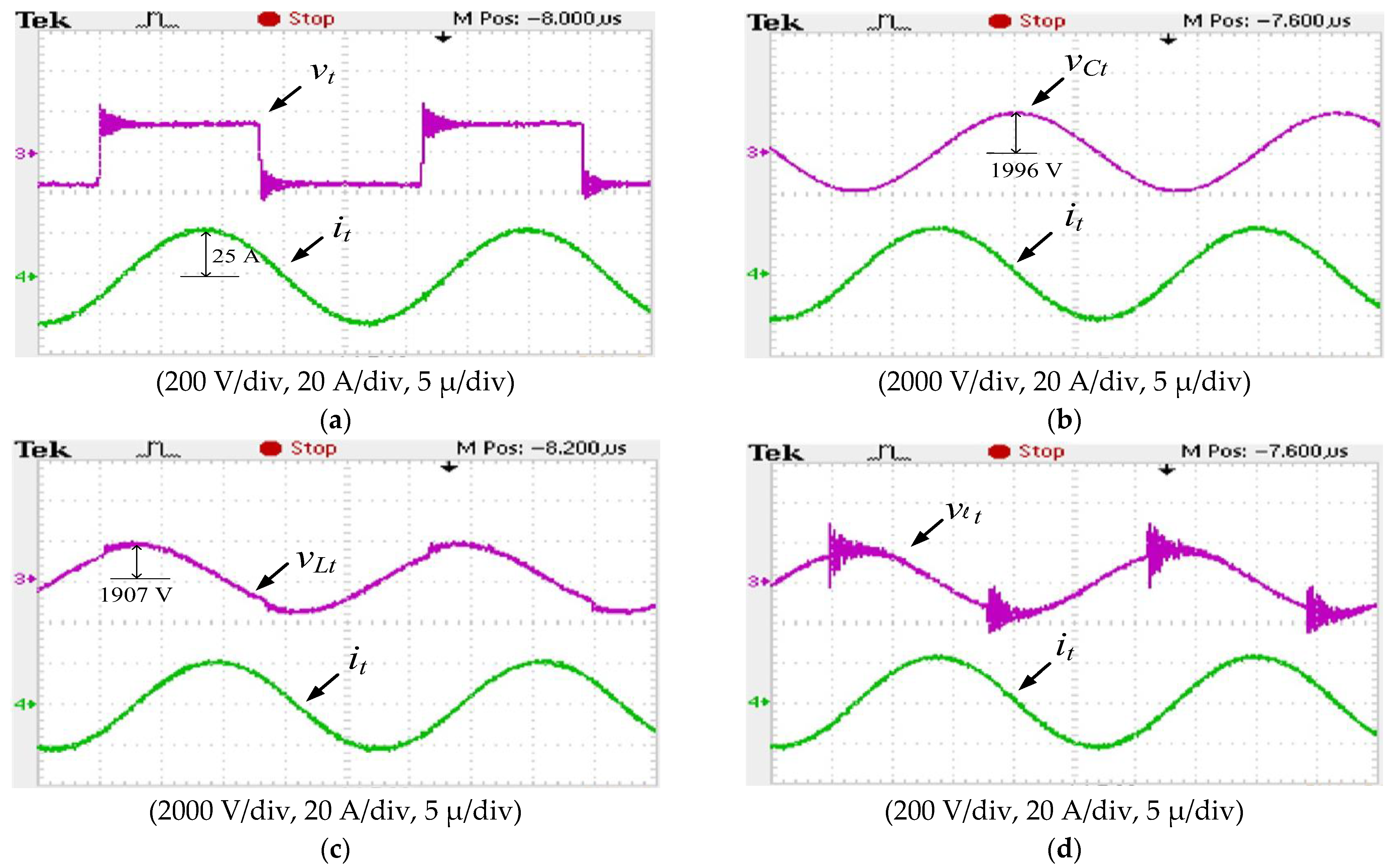
Measured waveforms of switches S1 and S3 under heavy load are shown in Figure 11, where the pink waveforms are the voltages, and the green ones are the currents. As indicated in Figure 11a,b, these switches performed ZVS operation to achieve soft switching. Figure 12 illustrates the measured waveforms of the components on the transmitter side, where the pink colors represent the voltage waveforms of different components on the transmitter side, and green ones represent the current on the transmitter side." Figure 12a shows the voltage vt and current it of the resonance tank on the transmitter side. The waveforms of voltage vt and current it reflect the switching statuses of the four active switches. Figure 12b presents the voltage and current of compensation capacitor Ct, indicating that the peak voltage reached nearly 2000 V. Figure 12c illustrates the measured voltage and current of the transmitting coil. The coil must withstand a voltage and current of approximately 4000 VP-P and 40 AP-P, respectively. Finally, Figure 12d displays the measured voltage and current waveforms of the air-core inductor t. The reason for the peak voltage oscillation in the figure was that the leakage inductance of the air-core inductor and the stray capacitance in the circuit oscillated when the active switch of the inverter was turned on.
Measured waveforms for each component on the receiver side are shown in Figure 13, where the pink colors represent the voltage waveforms of different components on the receiver side, and green ones represent the current on the receiver side. Figure 13a shows the voltage vr and current iCr of the resonant tank on the receiver side, and the peak value of the current iCr was approximately 32 A. The measured waveforms of the compensation capacitance Cr and the coil Lr are shown in Figure 13b,c, respectively. From Figure 13b, it can be seen that the peak voltage of the compensation capacitor Cr was approximately 1400 V, and the peak voltage of the coil Lr was approximately 1550 V. They illustrate that the second-order series resonant circuit was adopted for the proposed circuit, and the receiver side has a step-down characteristic. Thus, the large increase in charging current is beneficial for fast charging.
Figure 14 illustrates the measured waveforms of the rectifier diodes, where the pink color waveforms are the voltages, and the green ones are the currents. As indicated in Figure 14a, the voltage across the diode d1 was approximately 140 V, which was equivalent to the voltage of the two BESSs. The waveform of vd1 exhibited a slope, which was related to the voltage difference between the charge and discharge of the batteries; this can be explained using Equations (27)–(29). According to the measured waveforms displayed in Figure 14a,b, the rectifier diodes can achieve ZVS turn on and ZCS turn off, which are soft switching features.
The proposed high-efficiency sine-wave current pulses wireless charger was used to charge the two BESSs, and relevant charging data were recorded every 15 s. The recorded data included the charging voltages vb1 and vb2, charging currents ibl and ib2, and charging power and charging efficiency η. Figure 15 displays the charging voltages vb1 and vb2 of the BESSs, where the blue curves are the charging process voltage curve of BESSs, and the red circles are the initial voltage. The initial values of vb1 and vb2 were 59.45 V and 59.77 V, respectively. At the beginning of the charging process, the voltage difference between the charger and the batteries was large, resulting in an instantaneous increase in the current, and the voltages of the battery banks of b1 and b2 increased to 60.17 V and 60.50 V, respectively. Subsequently, the internal chemical reaction of the batteries became stable, and the voltages decreased and then increased. After the battery banks were charged for 1.61 h, the battery voltages approximated the rated value of 77.5 V, and charging was stopped. Specifically, the voltages of b1 and b2 after charging for 1.61 h were 77.53 V and 77.33 V respectively, which represented their full-charging voltages.
Figure 16 presents curves representing the charging currents of b1 and b2, where the black colors are the charging process current curve of BESSs, and the red circles are the initial current during charging. According to these curves, the currents at the beginning of the charging process were approximately 12 A. After approximately 3 min of charging, the charging currents were maintained at approximately 8–9 A. After approximately 1.1 h of charging, the charging currents of b1 and b2 decreased to approximately 8 A. Subsequently, the charging currents of the batteries gradually decreased until the charging time reached 1.61 h; at this time, the batteries were fully charged. The reason for the many current spikes in the figure was the active switch switches at a high frequency, which caused noise interference during signal sampling.
Figure 17 illustrates curves representing the charging power of the proposed charger, where the blue colors are the charging power curves, and the red circles are the initial charging power. According to these curves, the total charging power of the two BESSs under interleaved charging was up to 1391 W during the initial part of the charging process. This power then decreased to 835 W after 1.61 h of charging; at this time, the batteries were fully charged.
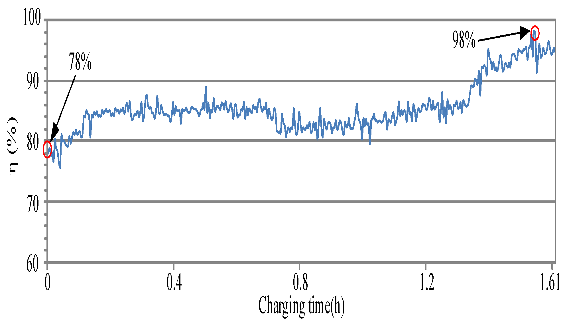
Figure 18 displays the charging efficiency of the proposed charger, where the blue color is the efficiency during charging, and the two red circles are the lowest and highest efficiency points respectively. As indicated in this figure, during the initial part of the charging process, the BESSs exhibited their lowest impedance, voltage, and capacity. Therefore, the voltage difference between the charger and batteries differed considerably, which resulted in the generation of a high charging current; thus, the initial charging efficiency was 78%, which was the lowest throughout the charging process. The voltages of the BESSs gradually increased with the charging current; consequently, the difference between the voltages of the charger and batteries gradually decreased, which resulted in a decrease in the charging current. The power provided by the charger gradually decreased as a result, and the charging efficiency increased. The highest charging efficiency was 98% and was achieved just before the end of the charging process. In addition, the charging current is relatively high when the battery is just being charged, which conforms to the characteristics of the high quality factor of the LLC converter. The conversion efficiency is poor when working under a heavy load condition. When the battery is close to being fully charged, the required charging current is small, which also complies with the low quality factor characteristic of the LLC converter, and has higher efficiency when operating under a light load condition.
During the charging period of the two BESSs, Figure 19 displays the temperature-measured curves of the batteries, where the blue colors represent the temperature curves of the upper and lower of the batteries, and the orange colors represent the ambient temperature. In Figure 19a, it illustrates the temperature curves of the BESS b1, including battery-surface temperature and ambient temperature. Initially, the temperature curve experiences a rapid ascent, primarily attributed to a substantial charging current of 12 A. At the 13.44 min mark, the peak temperature of 42.12 °C is reached. Subsequently, the curve exhibits a gradual decline, stabilizing within the range of 37 to 38 °C. As the BESS approaches full charge, the charging current diminishes progressively, resulting in a decreasing trend in the temperature curve. Correspondingly, Figure 19b displays the temperature curves of the BESS b2, encompassing battery-surface temperature and ambient temperature. The highest temperature, 41.93 °C, is recorded at the 14.1 min mark. Given that both BESSs utilized new batteries for the testing, the temperature curves exhibit similar patterns.
The transmitting and receiving coils of the proposed charger are, respectively, presented in Figure 20a–c, showing the 20 cm air gap between these coils. In Figure 20a,b, the red double arrows represent the inner diameter of the coils, and the orange double arrows represent the outer diameter of the coils. In Figure 20c, the red arrows point to the transmitting and the receiving coils respectively, and the red double arrows represent the coil distance. To fabricate the high-voltage compensation capacitors Ct and Cr, multiple metalized polypropylene film capacitors were connected in series and parallel, as shown in Figure 21a,b. Figure 21c depicts the air-core inductor t, which was wound with multistrand wires by using a plastic sleeve. The inductance of this inductor was measured to be 37 μH at a frequency of 50 kHz, and its quality factor Q was 78.

6. Conclusions

The paper comprehensively examines the operational principle, design process, and experimental waveform measurements related to the proposed charger. The experimental findings clearly illustrate that the LLC resonant tank efficiently converts input power, enabling the transmitter coil to achieve a substantial step-up in voltage. By adjusting the inductance ratio (K value), it is possible to restrict the circulating current at the transmitter side within a safe operational range. Furthermore, under a switching frequency of 37.9 kHz, the four active switches and two rectifier diodes exhibit soft switching characteristics. The receiving coil received a magnetic field from the transmitting coil over an air gap of 20 cm; the induced voltage has been significantly stepped down. Conversely, the current is augmented to facilitate the wireless charging of two BESSs with storage capacities of 60 V and 14 Ah, respectively. The recorded data reveals a maximum output power of 1391 W and an impressive charging efficiency of 98%. These results underscore the effectiveness of the circuit topology and charging method in optimizing green energy storage with minimal energy loss. This outcome presents a compelling solution to address the growing energy scarcity on Earth.
In contrast to conventional wireless chargers that typically employ LCC circuit topologies, combined with DC charging for fast charging, this study’s proposed charging strategy not only enhances charging efficiency but also prolongs the battery’s cycle life. This high-efficiency wireless charger has the potential to revolutionize the use of green energy sources, reducing our reliance on traditional power grids, curbing carbon emissions, and minimizing environmental impacts. Its applicability in electric vehicles, industrial automation, and smart homes stands to reduce energy wastage and offer greater convenience and scalability. In conclusion, efficient wireless chargers hold significant promise for improving energy efficiency and environmental protection. This, in turn, contributes to the sustainability of our energy resources, aligning with our broader goals of promoting a greener and more sustainable future.

Author Contributions

Conceptualization, Y.-C.C.; methodology, Y.-D.C.; validation, Y.-S.H.; formal analysis, Y.-D.C.; investigation, Y.-C.C.; resources, Y.-C.C.; data curation, Y.-D.C.; writing—original draft preparation, Y.-D.C.; writing—review and editing, Y.-D.C.; visualization, Y.-S.H.; supervision, Y.-C.C.; project administration, Y.-C.C.; All authors have read and agreed to the published version of the manuscript.

Funding

This research received no external funding.

Conflicts of Interest

The authors declare no conflict of interest.

References

  1. Brown, W.C. The history of power transmission by radio waves. IEEE Trans. Micro. Theory Tech. 1984, 32, 1230–1242. [Google Scholar] [CrossRef]
  2. Kurs, A.; Karalis, A.; Moffatt, R.; Joannopoulos, J.D.; Fisher, P.; Soljac, M. Wireless power transfer via strongly coupled magnetic resonances. Science 2007, 317, 83–86. [Google Scholar] [CrossRef] [PubMed]
  3. Karalis, A.; Joannopoulos, J.D.; Soljacicb, M. Efficient wireless non-radiative mid-range energy transfer. Ann. Phys. 2008, 323, 34–48. [Google Scholar] [CrossRef]
  4. Noeren, J.; Parspour, N. Lukas Elbracht, An Easily Scalable Dynamic Wireless Power Transfer System for Electric Vehicles. Energies 2023, 16, 3936. [Google Scholar] [CrossRef]
  5. Tran, D.H.; Vu, V.B.; Choi, W. Design of a High-Efficiency Wireless Power Transfer System with Intermediate Coils for the On-Board Chargers of Electric Vehicles. IEEE Trans. Power Electron. 2018, 33, 175–187. [Google Scholar] [CrossRef]
  6. Ramezani, A.; Farhangi, S.; Hossein, I.-E.; Farhangi, B.; Rahimi, R.; Moradi, G.R. Optimized LCC-Series Compensated Resonant Network for Stationary Wireless EV Chargers. IEEE Trans. Ind. Electron. 2019, 66, 2756–2765. [Google Scholar] [CrossRef]
  7. Park, Y.-J.; Jang, B.G.; Park, S.-M.; Ryu, H.-C.; Oh, S.J.; Kim, S.-Y.; Pu, Y.G.; Yoo, S.-S.; Hwang, K.C.; Yang, Y.; et al. A Triple-Mode Wireless Power-Receiving Unit With 85.5% System Efficiency for A4WP, WPC, and PMA Applications. IEEE Trans. Power Electron. 2018, 33, 175–187. [Google Scholar] [CrossRef]
  8. Yoo, J.-S.; Gil, Y.-M.; Ahn, T.-Y. High-Power-Density DC–DC Converter Using a Fixed-Type Wireless Power Transmission Transformer with Ceramic Insulation Layer. Energies 2022, 15, 9006. [Google Scholar] [CrossRef]
  9. Corti, F.; Reatti, A.; Nepote, A.; Pugi, L.; Pierini, M.; Paolucci, L.; Grasso, F.; Grasso, E.; Nienhause, M. A Secondary-Side Controlled Electric Vehicle Wireless Charger. Energies 2020, 13, 6527. [Google Scholar] [CrossRef]
  10. Nama, J.K.; Verma, A.K.; Srivastava, M.; Tomar, P.S. An Efficient Inductive Power Transfer Topology for Electric Vehicle Battery Charging. IEEE Trans. Ind. Appl. 2020, 56, 6925–6936. [Google Scholar] [CrossRef]
  11. Li, W.; Zhao, H.; Deng, J.; Li, S.; Mi, C.C. Comparison Study on SS and Double-Sided LCC Compensation Topologies for EV/PHEV Wireless Chargers. IEEE Trans. Veh. Technol. 2016, 65, 4429–4439. [Google Scholar] [CrossRef]
  12. Cui, S.; Liu, Z.Z.; Hou, Y.J.; Zeng, H.; Yue, Z.K.; Liang, L.H. Study on efficiency of different topologies of magnetic coupled resonant wireless charging system. Int. Conf. New Energy Future Energy Syst. 2017, 93, 012064. [Google Scholar] [CrossRef]
  13. Xu, S.; Wang, Z.; Chen, J.; Jiang, W. Research and Design of LC Series Resonant Wireless Power Transfer System with Modulation Control Method for Supercapacitor Charging in Linear Motion Systems. Energies 2022, 15, 6739. [Google Scholar] [CrossRef]
  14. Neto, P.B.L.; Saavedra, O.R.; Ribeiro, L.A.d.S. A Dual-Battery Storage Bank Configuration for Isolated Microgrids Based on Renewable Sources. IEEE Trans. Sustain. Energy 2018, 9, 1618–1626. [Google Scholar] [CrossRef]
  15. McKeon, B.B.; Furukawa, J.; Fenstermacher, S. Advanced Lead-Acid Batteries and the Development of Grid-Scale Energy Storage Systems. Proc. IEEE 2014, 102, 951–963. [Google Scholar] [CrossRef]
  16. Takeda, K.; Takahashi, C.; Arita, H.; Kusumi, N.; Amano, M.; Emori, A. Design of hybrid energy storage system using dual batteries for renewable applications. In Proceedings of the IEEE PES General Meeting Conference Exposition, National Harbor, MD, USA, 27–31 July 2014. [Google Scholar]
  17. Yang, Y.; Ye, Q.; Tung, L.J.; Greenleaf, M.; Li, H. Integrated Size and Energy Management Design of Battery Storage to Enhance Grid Integration of Large-Scale PV Power Plants. IEEE Trans. Ind. Electron. 2018, 65, 394–402. [Google Scholar] [CrossRef]
  18. Pablo, D.-C.; Jose Ignacio, M.-H.; Javier, C. A Microgrid Model with EV Demand Uncertainty and Detailed Operation of Storage Systems. IEEE Trans. Ind. Appl. 2022, 58, 2497–2511. [Google Scholar]
  19. Cheung, T.K.; Cheng, K.W.E.; Chan, H.L.; Ho, Y.L.; Chung, H.S.; Tai, K.P. Maintenance techiques for rechargeable battery using pulse charging. In Proceedings of the International Conference on Power Electronics Systems and Applications, Hong Kong, China, 12–14 November 2006; pp. 205–208. [Google Scholar]
  20. Lai, C.-M.; The, J.; Cheng, Y.-H.; Li, Y.-H. A reflex-charging based bidirectional DC charger for light electric vehicle and DC-microgrids. In Proceedings of the TENCON 2017–2017 IEEE Region 10 Conference, Penang, Malaysia, 5–8 November 2017. [Google Scholar]
  21. Lavety, S.; Keshri, R.K.; Chaudhari, M.A. Comparative Evaluation of Temperature Regulated Pulse and Reflex Charging. Annu. Conf. IEEE Ind. Electron. Soc. 2019, 1, 6337–6342. [Google Scholar]
  22. Bizhani, H.; Sani, S.K.H.; Rezazadeh, H.; Muyeen, S.M.; Rahmani, S. Modeling of an Optimum Fast Charging Multi-Step Constant Current Profile for Lead-Acid Batteries. IEEE Trans. Ind. 2023, 59, 2050–2060. [Google Scholar] [CrossRef]
  23. Alhaider, M.M.; Ahmed, E.M.; Aly, M.; Serhan, H.A.; Mohamed, E.A.; Ali, Z.M. New Temperature-Compensated Multi-Step Constant-Current Charging Method for Reliable Operation of Battery Energy Storage Systems. IEEE Access 2020, 8, 27961–27972. [Google Scholar] [CrossRef]
  24. Krieger, E.M.; Cannarella, J.; Arnold, C.B. A comparison of lead-acid and lithium-based battery behaviorand capacity fade in off-grid renewable charging applications. Energy 2013, 60, 492–500. [Google Scholar] [CrossRef]
  25. Al Zyoud, A.; Elhaija, W.A. Solar power lead battery storage solution using cycle recovery charging method. J. Energy Storage 2019, 25, 100843. [Google Scholar] [CrossRef]
  26. Kirchev, A.; Perrin, M.; Lemaire, E.; Karoui, F.; Mattera, F. Studies of the pulse charge of lead-acid batteries for PV applications Part I. Factors influencing the mechanism of the pulse charge of the positive plate. J. Power Sources 2008, 177, 217–225. [Google Scholar] [CrossRef]
  27. Mohamed, T.; Becetti, A.; Bayhan, S. Design and analysis of full bridge LLC resonant converter for wireless power transfer applications. In Proceedings of the IEEE International Conference on Compatibility Power Electronics Power Engineering, Doha, Qatar, 10–12 April 2018; pp. 1–5. [Google Scholar]
  28. Bosshard, R.; Kolar, J.W.; Mühlethaler, J.; Stevanović, I.; Wunsch, B.; Canales, F. Modeling and η-α-Pareto Optimization of Inductive Power Transfer Coils for Electric Vehicles. IEEE Trans. Emerg. Sel. Top. Power Electron. 2015, 3, 50–64. [Google Scholar] [CrossRef]
  29. Liao, C.; Li, J.; Li, S. Design of LCC impedance matching circuit for wireless power transfer system under rectifier load. IEEE Trans. Power Electron. Appl. 2017, 2, 237–245. [Google Scholar] [CrossRef]
  30. Ali, N.; Liu, Z.; Hou, Y.; Armghan, H.; Wei, X.; Armghan, A. LCC-S Based Discrete Fast Terminal Sliding Mode Controller for Efficient Charging through Wireless Power Transfer. Energies 2020, 13, 1370. [Google Scholar] [CrossRef]
  31. Yang, J.; Zhang, X.; Zhang, K.; Cui, X.; Jiao, C.; Yang, X. Design of LCC-S Compensation Topology and Optimization of Misalignment Tolerance for Inductive Power Transfer. IEEE Access 2020, 8, 191309–191318. [Google Scholar] [CrossRef]
  32. Wang, X.; Xu, J.; Ma, H.; Yang, P. A High Efficiency LCC-S Compensated WPT System with Dual Decoupled Receive Coils and Cascaded PWM Regulator. IEEE Trans. Circuits Syst. II Express Briefs 2020, 67, 3142–3146. [Google Scholar] [CrossRef]
  33. Krishnaswami, H.; Mohan, N. Three-Port Series-Resonant DC–DC Converter to Interface Renewable Energy Sources With Bidirectional Load and Energy Storage Ports. IEEE Trans. Power Electron. 2009, 24, 2289–2297. [Google Scholar] [CrossRef]
  34. Canales, F.; Barbosa, P.; Lee, F.C. A wide input voltage and load output variations fixed-frequency ZVS DC/DC LLC resonant converter for high-power applications. IEEE Ind. Appl. Conf. 2002, 4, 2306–2313. [Google Scholar]
  35. Roy, C.P. Control analysis of a high frequency resonant inverter for induction cooking application. Int. J. Res. Eng. Technol. 2015, 4, 340–348. [Google Scholar]
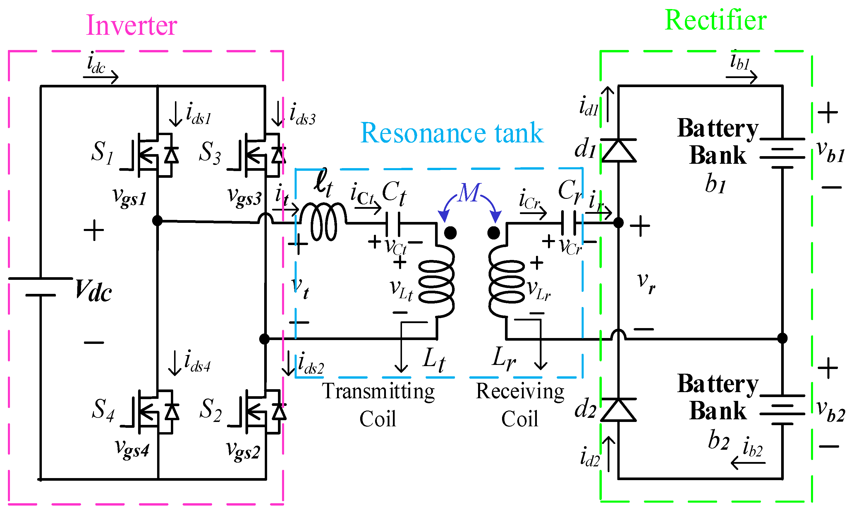
Figure 1. Circuit diagram of the proposed charger.
Energies 16 07102 g001
Figure 2. Key current and voltage waveforms of the proposed wireless interleaved charger.
Energies 16 07102 g002
Figure 3. Operational principle of the proposed high-efficiency sine-wave current pulses wireless charger.
Energies 16 07102 g003aEnergies 16 07102 g003b
Figure 4. Characteristic curves of a conventional LLC converter.
Energies 16 07102 g004
Figure 5. Efficiency Curves versus various loads.
Energies 16 07102 g005
Figure 6. DC-gain curves versus various inductance ratios.
Energies 16 07102 g006
Figure 7. Equivalent AC circuit of the proposed LLC-S wireless charger.
Energies 16 07102 g007
Figure 8. Schematic diagram of the interleaved sine-wave current pulses charging method.
Energies 16 07102 g008
Figure 9. Design flow chart of the proposed sine-wave current pulses wireless charger.
Energies 16 07102 g009
Figure 10. Conceptual block diagram of wireless power-transmission coils.
Energies 16 07102 g010
Figure 11. Measured voltage and current waveforms of the switches (a) S1 and (b) S3.
Energies 16 07102 g011
Figure 12. Measured waveforms of current it with (a) Voltage vt, (b) Voltage vCt, (c) Voltage vLt, and (d) Voltage vt waveforms on the transmitter side.
Energies 16 07102 g012
Figure 13. Measured current iCr with (a) Voltage vr, (b) Voltage vCr, and (c) Voltage vLr waveforms on the receiver side.
Energies 16 07102 g013aEnergies 16 07102 g013b
Figure 14. Measured voltage and current waveforms of the rectifier diodes (a) d1 and (b) d2.
Energies 16 07102 g014
Figure 15. Charging voltage curves of (a) battery bank b1 and (b) battery bank b2.
Energies 16 07102 g015
Figure 16. Charging-current curves of the (a) battery bank b1 and (b) battery bank b2.
Energies 16 07102 g016
Figure 17. Charging power curves of (a) battery bank b1 and (b) battery bank b2.
Energies 16 07102 g017
Figure 18. Conversion efficiency of the proposed charger during charging.
Energies 16 07102 g018
Figure 19. Charging temperature versus environment temperature curves of (a) battery bank b1 and (b) battery bank b2.
Energies 16 07102 g019
Figure 20. Photograph of the wireless (a) transmitting coil, (b) receiving coil, and (c) wireless coils with air gap.
Energies 16 07102 g020
Figure 21. Photograph of the resonance (a) compensation capacitors Ct, (b) compensation capacitors Cr, and (c) air-core inductor t.
Energies 16 07102 g021
Table 1. Comparison of performance indexes between half-bridge and full-bridge rectifiers.
Circuit Structure
Performance Index
Half-Bridge RectifierFull-Bridge Rectifier
Charging methodSine-wave current pulsesDC charging
Number of charging21
Diode24
LC filterNoneNeed
Rest time50% periodNone
Circuit structureDouble voltageRectifier
CostLowHigh
Table 2. Specification of the proposed charger.
SymbolParameterValue
VdcNominal input voltage155 V
fsSwitching frequency37.9 kHz
fmResonance frequency34 kHz
HgAir gap20 cm
PoRated output power1500 W
ib1Charging current5.4~12.6 A
ib2Charging current6.2~12.48 A
vb1Battery voltage59.45~77.53 V
vb2Battery voltage59.77~77.33 V
Table 3. Various parameters of the resonance tank.
SymbolParameterModel/Value
S1–S4Active switchIXTK120N65X2
D1–D2Rectifier DiodeIQBD60E60A1
LtTransmitting coil inductance400.4 μ H
LrReceiving coil inductance219.1 μ H
ltAir-core inductance37 μ H
KInductance ratio10.82
kCoupling coefficient0.45
CtTransmitting-side compensation capacitance0.05 μ F
CrReceiving-side compensation capacitance0.1 μ F
Table 4. Experimental equipment and instruments.
Option
Equipment
BrandModel
Power supplyGitekGR-15H20H
OscilloscopeTektronixTDS 2024B
Differential probeSanhuaLDP6110
Amplifier
Current probe
TektronixTCPA300
TCP312A
LCR meterMicrotest6376
BatteryYuasaREC14-12
Disclaimer/Publisher’s Note: The statements, opinions and data contained in all publications are solely those of the individual author(s) and contributor(s) and not of MDPI and/or the editor(s). MDPI and/or the editor(s) disclaim responsibility for any injury to people or property resulting from any ideas, methods, instructions or products referred to in the content.