Abstract
The DC-link capacitor in power electronic systems is one of the most vulnerable components in terms of reliability. Since a reliable design of the DC-link capacitor depends on an accurate estimation of its current ripple, this paper proposes analytical equations to model the influence of dead-time on the input current ripple of a three-phase voltage source inverter. The effect of dead-time is modeled as a delay in the rising edges of the input current waveform. The proposed analytical equations are derived and then verified by simulations and experiments. The proposed equations generally provide better accuracy in predicting the input current ripple value compared to the benchmark equations. From the simulation and experimental results, the proposed equations are optimized for dead-time values more than 0.7 s and modulation indices less than or equal to 0.7. Limitations of the proposed equations are also discussed. For small phase displacements and high modulation indices (0.8 to 1), the accuracy decreases because of the influence of AC output current ripple. For small modulation indices (less than 0.2) and a high value of dead-time (2 s), the accuracy also decreases due to distortion in the phase current waveforms.
1. Introduction
Three-phase Voltage Source Inverters (VSIs) are widely utilized in various applications such as photovoltaic systems, electric vehicles and electric drives [1]. The DC-link capacitor plays a crucial part to filter out the ripple component resulting from the PWM (pulse-width modulation) switching scheme in a three-phase VSI and as an energy buffer [2,3].
According to an industry-based survey, the DC-link capacitor in power electronic systems is one of the most vulnerable components in terms of reliability [4]. Since one of the critical stressors of the DC-link capacitor’s reliability is its rms current [1], a reliable design of the DC-link capacitor depends on an accurate estimation of its current ripple. This is well-acknowledged as a research problem. Reduction of the current ripple with modulation techniques [5,6,7], consideration of current ripple in the design procedure of DC-link capacitor [8,9,10] and calculation of the DC-link capacitor’s rms current ripple [11,12,13,14,15,16] are examples of research in line with the problem. The last topic is of interest here.
The calculation method of the input current ripple in a three-phase VSI generally falls into two categories: frequency-domain [11,12,13,14] and time-domain approaches [15,16]. The drawback of the former is the extra computational burden due to the inclusion of high-frequency components. The time-domain approach is simpler because the current ripple is modeled only as a function of rms phase current, modulation index and phase displacement. Owing to its simplicity, the time-domain approach is also easily extendable to the case of multiphase [17,18,19,20] and multilevel [21] inverters.
Despite its advantage over the frequency-domain approach, neither [15,16] nor their extensions take into account the influence of dead-time on the calculation of the input current ripple of a three-phase VSI, except in [22], which is the basis of this paper. In [23], the equation is extended to take into account the influence of diode’s reverse recovery on the input current ripple of a three-phase VSI. Other extensions include the influence of load unbalance in three-phase [24] and multiphase [25] inverters. The influence of output current ripple is addressed in [26]. A current control method that takes into account the capacitor current ripple is devised in [27]. However, all of the extensions assume the dead-time to be non-existent. Table 1 summarizes the state-of-the-art of the time domain approaches and their extensions. To the authors’ best knowledge, no attempt has been made to take into account the influence of dead-time to the calculation of the input current ripple of a three-phase VSI.

Table 1.
State-of-the-art of the time-domain approach.
Seminal attempts to consider the influence of dead-time on the current ripple in a three-phase VSI are made in [28,29]. However, they only address its effect on the negative spikes of the input current [28] or the dynamic behaviour of the DC-link capacitor in a rectifier–inverter circuit [29]. As far as the input current ripple value as is concerned (as in [15,16,17,18,19,20,21,22,23,24,25,26,27]), no reference has been made. Other research such as [30,31] are more focused on the dead-time compensation method in the control loop.
Therefore, this paper proposes analytical equations for the input current ripple of a three-phase VSI taking into account the influence of dead-time. The effect of dead-time is modeled as a delay in the rising edges of the input current waveform. The analytical equations are derived and then verified by simulations and experiments. It is shown that there is an inversely proportional relationship between the dead-time and the input current ripple values. Compared to the benchmark equations in [15], the proposed equations generally provide better accuracy in predicting the input current ripple value. From the simulation and experimental results, the proposed equations are optimized for dead-time values more than 0.7 s and modulation indices less than or equal to 0.7. Limitations of the proposed equations are also discussed. For small phase displacement and high modulation indices (0.8 to 1), the accuracy decreases because of the influence of AC output current ripple. For low modulation indices (less than 0.2) and a high value of dead-time (2 s), the accuracy also decreases due to distortion in the phase current waveforms.
The remainder of this paper is organized as follows: Section 2 shows the derivation of the analytical equations to calculate the input current ripple of a three-phase VSI considering the influence of dead-time. Section 3 provides verification of the proposed equations by simulations. Section 4 provides experimental verification. A GaN (Galium Nitride) transistors-based setup is used to diminish the effect of diodes reverse recovery, since the GaN transistor does not have an anti-parallel diode. Section 5 provides the conclusions of the paper.
2. Modelling the Influence of Dead-Time on the Input Current Ripple of a Three-Phase VSI
Figure 1 shows a typical three-phase VSI circuit supplying three-phase sinusoidal AC current (-) to a Y-connected RL load. The back-EMF (electromotive force) may also be present when modeling an AC-machine. However, it does not directly influence the calculation of the input current ripple. Thus, it is omitted from Figure 1 for simplicity. The reference signals (-) and the phase currents (-) in the three-phase VSI are expressed as
where m is the modulation index, is the sinusoidal AC phase current rms value, and is the phase displacement.
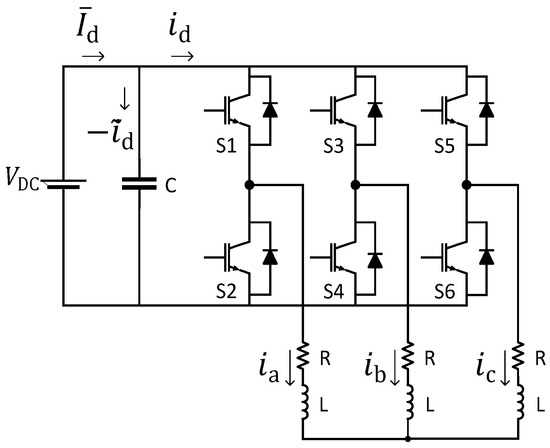
Figure 1.
Three-phase VSI circuit.
For bipolar modulation, the AC sinusoidal reference signals (-) are compared with a triangular carrier signal. If the carrier frequency is considerably higher than the AC frequency, the reference signals can be approximated by a straight line over a carrier period [15]. This is shown in Figure 2.
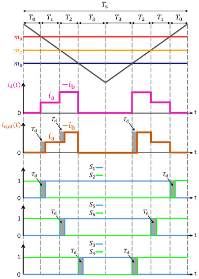
Figure 2.
Example of input current waveform of a three-phase VSI over a carrier period without ()/with the influence of dead-time () and the gating signals of the switches.
The intervals in Figure 2 can be expressed as a function of reference and carrier signals. These are written as:
where is the carrier period, and is the amplitude of the carrier signal.
Figure 2 also shows an example of the resulting input current waveform of the three-phase VSI over a carrier period without and with the influence of dead-time (), along with the gating signals of the switches. The switching occurrence is assumed to be instantaneous (ideal switching). Therefore, the effect of switching transients caused by parasitic inductance/capacitance in the power loop is not covered here since they will unnecessarily complicate the modeling.
It is shown that the dead-time only affects the rising edge of the waveform. This is because, at the rising edges, the current changes its path from the anti-parallel diode of one switch to the opposing semiconductor switch, i.e., hard switching. The switching event does not take place immediately due to the presence of dead-time, which causes a delay as shown in Figure 2. However, at the falling edge, the current changes its path from the switch to the diode immediately, i.e., soft switching. Therefore, there is no influence on the waveform of the input current.
The rising and falling edges depend on the direction of the current. However, the direction of the current depends highly on its load profile, which is a combination of the value of resistance (R), inductance (L) and the AC frequency (). In the following proposed equations, the effect of load change is indirectly represented by the value of phase displacement (). The derivation of the analytical equations of the input current ripple of a three-phase VSI is performed by taking into account all the possible phase displacements which causes different rising and falling edge scenarios. This can be divided into two cases: ≤ and > .
2.1. Case 1: ≤
Figure 3 shows the input current waveform for different intervals in case 1. For Figure 3a, the input current () waveform per interval is obtained as:
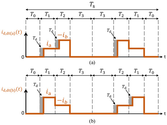
Figure 3.
Input current waveform of a three-phase VSI (case 1: ≤ ) for intervals: (a) ≤ t ≤ + ; (b) + ≤ t ≤ .
Similarly, for Figure 3b, the input currents () per interval are obtained:
Taking (11) and (12) into account, respectively, the squared input current expressions over a carrier period are written as:
From (13) and (14), the rms input current of the three-phase VSI considering the influence of dead-time () is obtained as follows:
where is the ideal rms input current of the three-phase VSI, and is the influence of dead-time on the rms input current.
To obtain the rms value of the ripple component flowing through the DC-link capacitor, Equation (15) must be subtracted from its DC component. Therefore, the expression for the rms value of the input current ripple of a three-phase VSI considering the influence of dead-time is written as:
where is the DC component of the input current of a three-phase VSI.
2.2. Case 2: >
Figure 4 shows the input current waveform for different intervals in case 2. The input current expressions are obtained as:
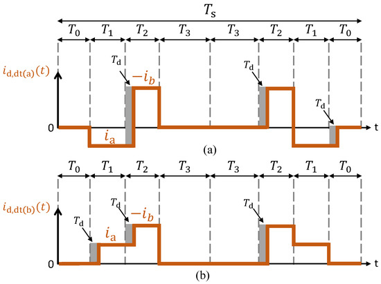
Figure 4.
Input current waveform of a three-phase VSI (case 2: > ) for intervals: (a) ≤ t ≤ ; (b) ≤ t ≤ .
3. Simulation Results
Table 2 shows the system parameters of the three-phase VSI used for the simulation verifications. Two load profiles are used for the verification of (18) for case 1 and case 2 loads. They represent all possible load scenarios which affects the calculation of the input current ripple.
Table 2.
System parameters of the three-phase VSI used for simulation.
From (17), it is shown that the ratio of and plays a part in determining the influence of dead-time on the rms input current. Thus, there are two ways to verify the influence of dead-time: (1) keep the constant and vary the value of ; (2) keep the constant and vary . In this paper, the first approach is used for both simulation and experimental verifications. It is also to be noted that, according to [15], the value of must be at least nine times higher than for the equations to hold on. Since, in Table 2, is 200 times higher than , the constraint is fulfilled.
3.1. Case 1 Load ( ≤ )
Figure 5 shows the calculation and simulation results of the rms input current ripple of the three-phase VSI as the modulation index is varied. is set to 0.1 s. It is shown that the calculation values from (16)–(18) match the simulation results.
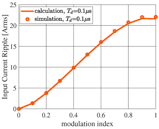
Figure 5.
Calculation and simulation results of modulation index vs. rms input current ripple of the three-phase VSI (case 1 load, = 0.1 s).
However, from Figure 5 alone, it is difficult to see the influence of dead-time to the reduction of the rms input current ripple of the three-phase VSI, as (18) indicates. Therefore, Figure 6 shows the variation of the rms input current ripple value with respect to the value of dead-time.
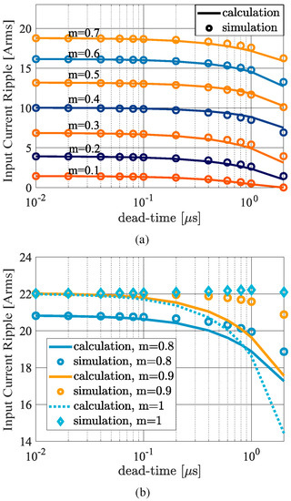
Figure 6.
Calculation and simulation results of dead-time vs. rms input current ripple of the three-phase VSI (case 1 load) for (a) 0.1 ≤ m ≤ 0.7; (b) 0.8 ≤ m ≤ 1.
Figure 6 shows the trend of decreasing rms input current ripple with the increase of dead-time for varying modulation index. The reduction is typically between 15% to 45% depending on the modulation index for = 2 s. For 0.1 ≤ m ≤ 0.7 (Figure 6a), it is shown that the proposed equations match the simulation results closely. However, the accuracy becomes worse for high modulation indices, i.e., 0.8 ≤ m ≤ 1 (Figure 6b). This can be explained by referring to [26]. It is observed in [26] that, for high modulation index (m) and low phase displacement (), the output current ripple becomes higher. This adds up to the total rms input current ripple, which diminishes the influence of dead-time and makes the calculation results deviate from the simulation results.
Figure 7a,b show the absolute error percentage of the benchmark and proposed equations compared to the simulation results. Figure 7c shows the accuracy improvement of the proposed equations compared to the benchmark equations. It is obtained by subtracting the error percentage of the benchmark equations with its proposed equations’ counterpart. If the net result is positive, it means there is an improvement in accuracy. If negative, it means that the proposed equations perform worse for the given point/area. In Figure 7c, the negative net results are marked by the white area, regardless of the values.
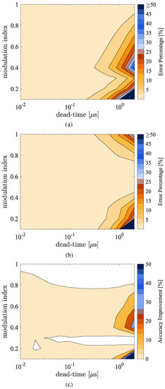
Figure 7.
Absolute error percentage of the (a) benchmark and (b) proposed equations; (c) relative improvement of the proposed equations compared to the benchmark equations (case 1 load, simulation).
From Figure 7c, it is shown that generally the proposed equations provide better accuracy than the benchmark equations. The significant improvement is shown when ≥ 0.7 s and 0.4 ≤ m ≤ 0.7. For m ≥ 0.8, the accuracy is worse due to the output current ripple influence (as explained previously). There is also a slight inaccuracy when m = 0.3 across a wide range of dead-time. However, the difference is minimum (less than 1%) and thus can be ignored.
For the bottom-left area (m ≤ 0.2 and ≥ 1 s), it might seem counter-intuitive that the improvement is significant in Figure 7c, whereas Figure 7a,b show a huge error in the same area. This is because the definition of error percentage in this paper is the absolute value of the difference between simulation and calculation results divided by the simulation result. Therefore, for low values of , the error is very large because the denominator is low, even if the actual difference is small (as shown in Figure 6a). The proposed equations increase the accuracy significantly. However, because of the definition of the error percentage, the overall error is still perceived as large as in Figure 7b. This holds true for all cases (case 1 and case 2 loads, simulations and experiments) and thus will only be explained here.
3.2. Case 2 Load ( > )
Figure 8 shows the verification of Equation (18) by simulations for the case 2 load with = 0.1 s. It is shown that the calculation results are in agreement with the simulation trends.
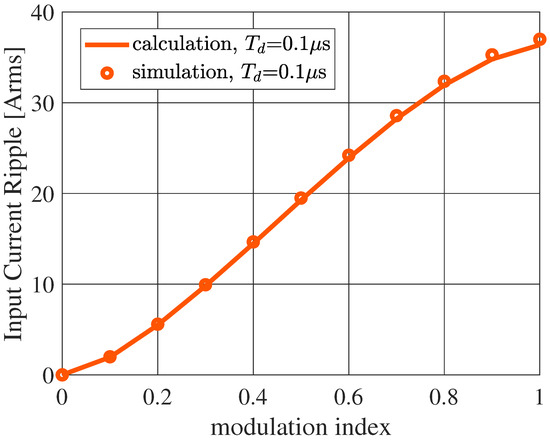
Figure 8.
Calculation and simulation results of modulation index vs. rms input current ripple of the three-phase VSI (case 2 load, = 0.1 s).
Figure 9 also shows the same trend of the decrease of rms input current ripple value with the increase of dead-time. The reduction is typically between 20% to 60% depending on the modulation index for = 2 s. The proposed equations are able to predict the simulation trends, and in this case the accuracy is not compromised for high modulation indices. This is because the phase displacement () is higher in the case 2 load, which decreases the AC output current of the three-phase VSI [26]. Therefore, the accuracy of the proposed equations holds on.
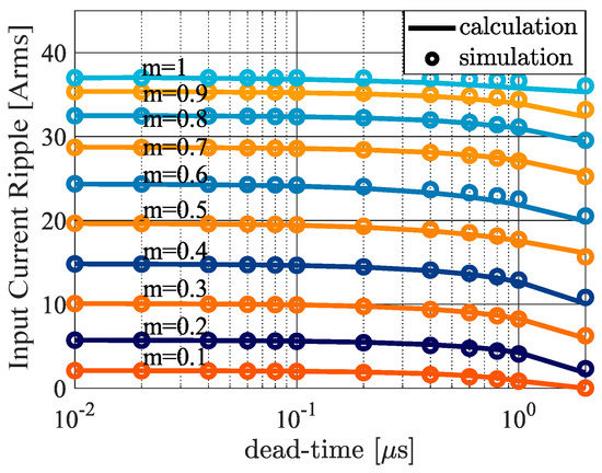
Figure 9.
Calculation and simulation results of dead-time vs. rms input current ripple of the three-phase VSI (case 2 load).
Figure 10a,b show the absolute error percentage of the benchmark and proposed equations for the case 2 load, whereas Figure 10c shows their accuracy comparison. For case 2 load (simulation), the accuracy of the proposed equations is better across all regions. The small white area on the middle-left can be disregarded as the difference is less than 0.5%. In ≥ 0.2 s regions, the accuracy of the proposed equations improves significantly.
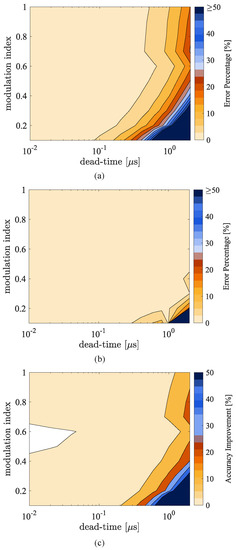
Figure 10.
Absolute error percentage of the (a) benchmark and (b) proposed equations; (c) relative improvement of the proposed equations compared to the benchmark equations (case 2 load, simulation).
4. Experimental Results
Table 3 and Figure 11 show the system parameters and the experimental setup used for verification of the equations, respectively. GaN transistors are used to avoid the influence of diode’s reverse recovery on the calculation of the rms input current ripple. An SDN-414-10 shunt resistor is used for its high bandwidth (2000 MHz) and relatively low rise time (0.18 ns), which is essential in capturing both the input current waveform and rms value of the capacitor current ripple. However, since the maximum dissipation of the shunt is relatively low, the power level for the experimental testbench is severely limited. Therefore, 30 V is chosen for . Nevertheless, the equations should also work for higher voltage/current, as shown in the simulation results for higher voltage (400 V). The proposed equations only depend on the modulation index (m), phase displacement (), and the ratio between dead-time () and switching period (). The selection of should not affect their accuracy.
Table 3.
System parameters of the three-phase VSI used for experiments.
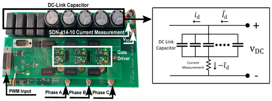
Figure 11.
Experimental setup for the three-phase VSI.
Figure 12 shows examples of the capacitor current ripple waveform produced by the three-phase VSI. It is shown that Figure 12a–c are able to reproduce the theoretical waveforms shown in Figure 3a, Figure 4b, Figure 3b, and Figure 4a, respectively. It should be noted that there is a difference in offset between the theoretical waveforms to the ones shown in Figure 12. This is due to the measurement being performed at the DC-link capacitor, which already excludes the DC component (see Equation (19)) of the input current waveform inherent in Figure 3 and Figure 4. However, the basic shape of the waveforms remains.
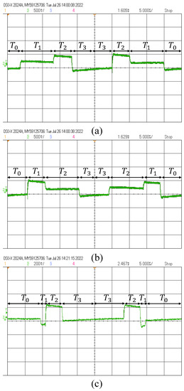
Figure 12.
Examples of capacitor current ripple waveform of a three-phase VSI for: (a) ≤ t ≤ + (case 1) & ≤ t ≤ (case 2) (b) + ≤ t ≤ (case 1) (c) ≤ t ≤ (case 2).
Figure 13 shows an example of the influence of the dead-time on the delay in the capacitor current waveform of the three-phase VSI. As previously indicated in Figure 2, the dead-time will only influence the rising edge of the waveform. This is also shown in Figure 13, where only the rising edges are affected. However, it should be noted that, in the experimental setup, a minimum value of dead-time still needs to be applied to avoid short circuit. Therefore, the “ideal” reference in Figure 13 (blue line) is actually using = 40 ns. Nevertheless, Figure 13 still satisfactorily shows that the dead-time only influences the rising edge of the waveform, thus confirming the initial theory.
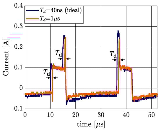
Figure 13.
Example of the influence of dead-time to the delay in the capacitor current waveform of three-phase VSI.
4.1. Case 1 Load ( ≤ )
Figure 14 shows the calculation and experimental results of the rms input current ripple of the three-phase VSI as the modulation index is varied. = 0.1 s is also used here. It is shown that the calculation values from (18) are in agreement with the experimental results.
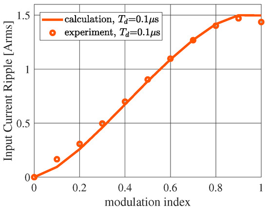
Figure 14.
Calculation and experimental results of modulation index vs. rms input current ripple of the three-phase VSI (case 1 load, = 0.1 s).
Figure 15 shows the influence of the increasing value of dead-time to the decrease in the rms input current ripple values. The decrease is typically in the range of 15% to 50% for = 2 s. Once again, the calculation results are in agreement with the experimental results up to m = 0.7. For higher modulation indices, the accuracy is worse due to the influence of the AC current ripple, as shown in the simulation results for the same load profile.
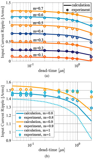
Figure 15.
Calculation and experimental results of dead-time vs. rms input current ripple of the three-phase VSI (case 1 load) for (a) 0.1 ≤ m ≤ 0.7; (b) 0.8 ≤ m ≤ 1.
Figure 16a,b show the absolute error percentage of the benchmark and proposed equations. Figure 16c shows their accuracy comparison. Similar to the simulation results, it is shown that, for m ≥ 0.8, the accuracy of the proposed equations is worse due to the influence of the output current ripple. For ≥ 0.5 s and m ≤ 0.7, the accuracy of the proposed equations increases significantly. This is in agreement with the simulation results where the proposed equations are optimized for ≥ 0.7 s and 0.4 ≤ m ≤ 0.7. Finally, the bottom-left white area (which signifies the worse accuracy for the proposed equations) is shown in Figure 16c. It is likely to be caused by the measurement error due to the noise captured by the scope, as it also appears in Figure 19c. It is to be noted that the current ripple values in that region is relatively low. Combined with the presence of measurement noise in the scope, the errors add up. However, it should be noted that the accuracy decrease are only around 1–2% in the bottom-left region. Nevertheless, from Figure 15a, it is shown that the proposed equations are still able to match the experimental results trend.
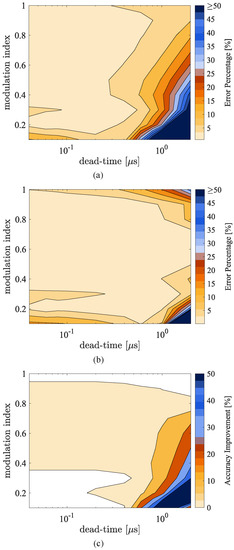
Figure 16.
Absolute error percentage of the (a) benchmark and (b) proposed equations; (c) relative improvement of the proposed equations compared to the benchmark equations (case 1 load, experiment).
4.2. Case 2 Load ( > )
Figure 17 shows the calculation and experimental results of the rms input current ripple of the three-phase VSI as the modulation is varied with = 0.1 s. Once again, it is shown that the calculation values from (18) are in agreement with the experimental results. Therefore, the proposed equations for both case 1 and case 2 loads have been verified by simulation and experimental results.
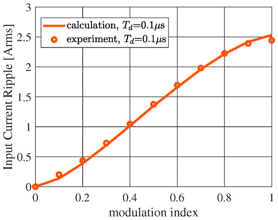
Figure 17.
Calculation and experimental results of modulation index vs. rms input current ripple of the three-phase VSI (case 2 load, = 0.1 s).
Figure 18 shows the influence of an increasing value of the dead-time on the decrease of rms input current ripple values. The decrease is typically between 15% to 45% for = 2 s. The calculation results are in agreement with the experimental results. There is a slight when the modulation index is 1. However, the trend-line still fits the calculation results. The offset is probably caused by a slight change in the shunt resistance value due to its error tolerance (±4%) [32] multiplied by high current because the experimental results follow the calculations trend but with consistent offset.
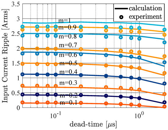
Figure 18.
Calculation and experimental results of dead-time vs. rms input current ripple of the three-phase VSI (case 2 load).
Figure 19a,b show the absolute error percentage of the benchmark and proposed equations for the case 2 load (experiment). Figure 19c shows their accuracy comparison. With the exception of the bottom-left area (as in case 1 load, experiment), it is shown in Figure 19c that the proposed equations generally provide better accuracy, especially when ≥ 0.4 s. This is similar to the simulation results where the proposed equations provide significant improvement in accuracy when ≥ 0.2 s.
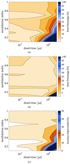
Figure 19.
Absolute error percentage of the (a) benchmark and (b) proposed equations; (c) relative improvement of the proposed equations compared to the benchmark equations (case 2 load, experiment).
5. Conclusions
This paper provides analytical equations to model the influence of dead-time to the rms value of the input current ripple of a three-phase VSI. The effect of dead-time is modeled as a delay in the rising edge of the input current waveform. The proposed equations have been verified by both simulations and experiments. It is shown that there is an inversely proportional relationship between the value of dead-time and the rms input current ripple, with the decrease of the latter because of the former are observed to be in the range of 15% to 60% for a dead-time of 2 s. For the simulation and experimental system parameters used in this paper, the proposed equations are also able to give higher accuracy in predicting the rms input current ripple value compared to the benchmark equations, especially for dead-time values more than 0.7 s and modulation indices less than or equal to 0.7. The proposed equations tend to perform better in the case 2 load. For the case 1 load, the proposed equations are optimized for modulation indices below 0.8 and dead-time over 0.7 s. For the case 2 load, the equations are optimized for dead-time over 0.4 s no matter the modulation index.
Limitations of the proposed equations are also discussed. For small phase displacement and high modulation indices (0.8 to 1), the accuracy decreases because the AC output current ripple increases the value of the rms input current ripple. For modulation indices less than 0.2 and a high value of dead-time (i.e., 2 s), the accuracy also decreases because of the distortion in the phase current waveforms.
Author Contributions
Conceptualization, J.A., J.L.D., H.H. and E.I.C.; Simulation, J.A.; Prototyping, J.A. and D.V.R.; Experiment, J.A. and D.V.R.; Writing, J.A.; Pictures, J.A. and D.V.R.; Internal review and proofreading, J.L.D., E.I.C. and H.H. All authors have read and agreed to the published version of the manuscript.
Funding
This research received no external funding.
Institutional Review Board Statement
Not applicable.
Informed Consent Statement
Not applicable.
Data Availability Statement
Not applicable.
Conflicts of Interest
The authors declare no conflict of interest.
Abbreviations
The following abbreviations are used in this manuscript:
| VSI | Voltage Source Inverter |
| PWM | Pulse-Width Modulation |
| DC | Direct Current |
| AC | Alternating Current |
| GaN | Galium Nitride |
| EMF | Electromotive Force |
| rms | Root Mean Square |
References
- Wang, H.; Blaabjerg, F. Reliability of Capacitors for DC-Link Applications in Power Electronic Converters—An Overview. IEEE Trans. Ind. Appl. 2014, 50, 3569–3578. [Google Scholar] [CrossRef]
- Lee, W.; Sul, S. DC-Link Voltage Stabilization for Reduced DC-Link Capacitor Inverter. IEEE Trans. Ind. Appl. 2014, 50, 404–414. [Google Scholar]
- Vujacic, M.; Dordevic, O.; Grandi, G. Evaluation of DC-Link Voltage Switching Ripple in Multiphase PWM Voltage Source Inverters. IEEE Trans. Power Electron. 2020, 35, 3478–3490. [Google Scholar] [CrossRef]
- Yang, S.; Bryant, A.; Mawby, P.; Xiang, D.; Ran, L.; Tavner, P. An Industry-Based Survey of Reliability in Power Electronic Converters. IEEE Trans. Ind. Appl. 2011, 47, 1441–1451. [Google Scholar] [CrossRef]
- Kieferndorf, F.D.; Forster, M.; Lipo, T.A. Reduction of DC-bus capacitor ripple current with PAM/PWM converter. IEEE Trans. Ind. Appl. 2004, 40, 607–614. [Google Scholar] [CrossRef]
- Hobraiche, J.; Vilain, J.; Macret, P.; Patin, N. A New PWM Strategy to Reduce the Inverter Input Current Ripples. IEEE Trans. Power Electron. 2009, 24, 172–180. [Google Scholar] [CrossRef]
- Nguyen, T.D.; Patin, N.; Friedrich, G. Extended Double Carrier PWM Strategy Dedicated to RMS Current Reduction in DC Link Capacitors of Three-Phase Inverters. IEEE Trans. Power Electron. 2014, 29, 396–406. [Google Scholar] [CrossRef]
- Anwar, M.N.; Teimor, M. An analytical method for selecting DC-link-capacitor of a voltage stiff inverter. In Proceedings of the Conference Record of the 2002 IEEE Industry Applications Conference 37th IAS Annual Meeting (Cat. No.02CH37344), Pittsburgh, PA, USA, 13–18 October 2002. [Google Scholar]
- Wen, H.; Xiao, W.; Wen, X.; Armstrong, P. Analysis and Evaluation of DC-Link Capacitors for High-Power-Density Electric Vehicle Drive Systems. IEEE Trans. Veh. Technol. 2012, 61, 2950–2964. [Google Scholar]
- Callegaro, A.D.; Guo, J.; Eull, M.; Danen, B.; Gibson, J.; Preindl, M.; Bilgin, B.; Emadi, A. Bus Bar Design for High-Power Inverters. IEEE Trans. Power Electron. 2018, 33, 2354–2367. [Google Scholar] [CrossRef]
- Ziogas, P.D.; Photiadis, P.N.D. An Exact Input Current Analysis of Ideal Static PWM Inverters. IEEE Trans. Ind. Appl. 1983, IA-19, 281–295. [Google Scholar] [CrossRef]
- Ziogas, P.D.; Wiechmann, E.P.; Stefanovic, V.R. A Computer-Aided Analysis and Design Approach for Static Voltage Source Inverters. IEEE Trans. Ind. Appl. 1985, IA-21, 1234–1241. [Google Scholar] [CrossRef]
- Bierhoff, M.H.; Fuchs, F.W. DC-Link Harmonics of Three-Phase Voltage-Source Converters Influenced by the Pulsewidth-Modulation Strategy—An Analysis. IEEE Trans. Ind. Electron. 2008, 55, 2085–2092. [Google Scholar] [CrossRef]
- McGrath, B.P.; Holmes, D.G. A General Analytical Method for Calculating Inverter DC-Link Current Harmonics. IEEE Trans. Ind. Appl. 2009, 45, 1851–1859. [Google Scholar] [CrossRef]
- Dahono, P.A.; Sato, Y.; Kataoka, T. Analysis and minimization of ripple components of input current and voltage of PWM inverters. IEEE Trans. Ind. Appl. 1996, 32, 945–950. [Google Scholar] [CrossRef]
- Kolar, J.; Round, S. Analytical calculation of the RMS current stress on the DC-link capacitor of voltage-PWM converter systems. IEE Proc. Elect. Power Appl. 2006, 153, 535–543. [Google Scholar] [CrossRef]
- Muqorobin, A.; Dahono, P.A. Input Current Ripple Analysis of Multiphase PWM Inverters. In Int. J. Power Electron. Drive Syst. 2018, 9, 1432–1444. [Google Scholar] [CrossRef]
- Arrozy, J.; Huisman, H.; Duarte, J.L. Input Current Ripple Analysis of Six-Phase Full-Bridge Inverters. In Proceedings of the 2021 IEEE 12th Energy Conversion Congress & Exposition-Asia (ECCE-Asia), Singapore, 24–27 May 2021. [Google Scholar]
- Dahono, P.A.; Satria, A.; Nurafiat, D. Analysis of DC current ripple in six-legs twelve-devices inverters. In Proceedings of the 2012 International Conference on Power Engineering and Renewable Energy (ICPERE), Bali, Indonesia, 3–5 July 2012. [Google Scholar]
- Taha, W.; Azer, P.; Poorfakhraei, A.; Dhale, S.; Emadi, A. Comprehensive Analysis and Evaluation of DC-Link Voltage and Current Ripples in Symmetric and Asymmetric Two-Level Six-Phase Voltage Source Inverters. IEEE Trans. Power Electron. 2022, 38, 2215–2229. [Google Scholar] [CrossRef]
- Orfanoudakis, G.I.; Yuratich, M.A.; Sharkh, S.M. Analysis of dc-link capacitor current in three-level neutral point clamped and cascaded H-bridge inverters. IET Power Electron. 2013, 6, 1376–1389. [Google Scholar] [CrossRef]
- Arrozy, J.; Retianza, D.V.; Huisman, H.; Duarte, J.L. Influence of Dead-Time and Diode’s Reverse Recovery on the Input Current Ripple of Three-phase Voltage Source Inverters. In Proceedings of the 2022 International Power Electronics Conference (IPEC-Himeji 2022-ECCE Asia), Himeji, Japan, 15–19 May 2022. [Google Scholar]
- Guo, J.; Ye, J.; Emadi, A. DC-Link Current and Voltage Ripple Analysis Considering Antiparallel Diode Reverse Recovery in Voltage Source Inverters. IEEE Trans. Power Electron. 2018, 33, 5171–5180. [Google Scholar] [CrossRef]
- Pei, X.; Zhou, W.; Kang, Y. Analysis and Calculation of DC-Link Current and Voltage Ripples for Three-Phase Inverter With Unbalanced Load. IEEE Trans. Power Electron. 2015, 30, 5401–5412. [Google Scholar] [CrossRef]
- Vujacic, M.; Dordevic, O.; Mandrioli, R.; Grandi, G. DC-link low-frequency current and voltage ripple analysis in multiphase voltage source inverters with unbalanced load. IET Electr. Power Appl. 2022, 16, 300–314. [Google Scholar] [CrossRef]
- Li, Q.; Jiang, D. DC-link current analysis of three-phase 2L-VSI considering AC current ripple. IET Power Electron. 2018, 11, 202–211. [Google Scholar] [CrossRef]
- Raab, S.; Krämer, A.; Ackva, A. Determination of RMS current load on the DC-link capacitor of voltage source converters using direct current control. IEEE Trans. Power Electron. 2020, 36, 968–977. [Google Scholar] [CrossRef]
- Chan, C.C.; Chau, K.T.; Li, Y. A novel dead-time vector approach to analysis of DC link current in PWM inverter drives. In Proceedings of the APEC 97—Applied Power Electronics Conference, Atlanta, GA, USA, 27 February 1997. [Google Scholar]
- Guha, A.; Narayanan, G. Impact of Dead Time on Inverter Input Current, DC-Link Dynamics, and Light-Load Instability in Rectifier-Inverter-Fed Induction Motor Drives. IEEE Trans. Ind. Appl. 2018, 54, 1414–1424. [Google Scholar] [CrossRef]
- Ren, R.; Zhang, F.; Liu, B.; Wang, F.; Chen, Z.; Wu, J. A closed-loop modulation scheme for duty cycle compensation of PWM voltage distortion at high switching frequency inverter. IEEE Trans. Ind. Electron. 2019, 67, 1475–1486. [Google Scholar] [CrossRef]
- Wang, L.; Xu, J.; Chen, Q.; Chen, Z.; Geng, X.; Lin, K. Improved PWM Strategies to Mitigate Dead-Time Distortion in Three-Phase Voltage Source Converter. IEEE Trans. Power Electron. 2022, 37, 14692–14705. [Google Scholar] [CrossRef]
- Powertek UK. Non Inductive Co-Axial Current Shunt SDN-414. 2022. Available online: https://powertekuk.com/coaxial-shunt-series-sdn-414#:~:text=The%20Series%20SDN%2D414%20range,measurements%20and%20power%20calibration%20systems (accessed on 23 August 2022).
Disclaimer/Publisher’s Note: The statements, opinions and data contained in all publications are solely those of the individual author(s) and contributor(s) and not of MDPI and/or the editor(s). MDPI and/or the editor(s) disclaim responsibility for any injury to people or property resulting from any ideas, methods, instructions or products referred to in the content. |
© 2023 by the authors. Licensee MDPI, Basel, Switzerland. This article is an open access article distributed under the terms and conditions of the Creative Commons Attribution (CC BY) license (https://creativecommons.org/licenses/by/4.0/).