Article

New Modular Multilevel DC–DC Converter Derived from Modified Buck–Boost DC–DC Converter

School of Electrical Engineering and Informatics, Institut Teknologi Bandung, Kota Bandung 40132, Indonesia
*
Author to whom correspondence should be addressed.
Deceased author.
Energies 2023, 16(19), 6950; https://doi.org/10.3390/en16196950
Submission received: 30 August 2023 / Revised: 25 September 2023 / Accepted: 1 October 2023 / Published: 4 October 2023

Abstract

:
Raising the electrification ratio to 100% is still a formidable challenge in Indonesia, especially in the remote areas of the eastern part of the archipelago. A DC microgrid system is one of the most viable solutions to increase the electricity supply in remote areas, taking advantage of various renewable energy sources that are located near the rural load centers. A DC–DC power converter for a rural DC microgrid system needs to have a high voltage gain to facilitate the power conversion from low-voltage PV output to a high-voltage DC microgrid bus, a very low input ripple current to help maintain the PV or battery lifetime, and be highly modular for ease of transport and assembly. Many topologies have been proposed to obtain high voltage gain, very low ripple current, and modularity. However, they usually use either bulky and lossy magnetic components, are sensitive to component parameter variance and need special voltage-balancing techniques, or have different component ratings for their multilevel configuration which weakens the modularity aspect. This paper proposes a new modular multilevel DC–DC converter that is very suitable for rural DC microgrid applications based on a modified buck–boost topology. The proposed converter is easily stackable to achieve high voltage gain and does not require any voltage balancing techniques, thus enhancing the modularity characteristics and simplifying its control method. Moreover, the ripple current can be reduced by employing a multiphase configuration. This converter can also facilitate bidirectional power flow to serve as a battery charger/discharger. A comprehensive analysis of voltage gain and ripple current are presented to explain the inner workings of this converter. Finally, the performance of this converter is verified through simulation and experiment, showing the converter’s modularity, bidirectional power capability, and potential to achieve voltage gain and ripple-current requirements of the DC microgrid system.

1. Introduction

Indonesia is an archipelago consisting of more than 17,000 islands. Although the electrification ratio in Indonesia has reached 99% in 2022, remote areas in Eastern Indonesia still do not have access to electricity. There are multidimensional causes for this problem, ranging from technical issues, such as lack of infrastructure, to sociocultural issues involving local traditions and beliefs. One of the most viable solutions to providing electricity to remote areas is dispersed generation. By using small power plants, electricity needs can be fulfilled by nearby energy sources, such as solar and wind power, effectively eliminating the need to build electrical connections to the main grid. Small power plants also do not require a large area. This is beneficial for minimizing the risk of harming the natural environment and defiling the traditional inheritance of the local community.
A DC microgrid has several advantages over an AC microgrid for remote areas. Firstly, load type in remote areas is predominated by domestic ones, such as lighting and electronic appliances, which benefit from DC power as well as AC power. Secondly, the highly available renewable energy source in Indonesia is sunlight harnessed through PV panels that produce DC power. Thirdly, the DC microgrid is simpler due to the absence of reactive power and synchronization. Therefore, the DC microgrid will be the focus of application for the remainder of this paper.
Figure 1 shows a DC microgrid system with PV panels as the energy source. The DC bus voltage is 400 VDC for easy conversion to 220 VAC if needed. DC–DC converters are used to connect PV panels, batteries, and DC loads to the DC bus. PV panels usually produce low voltage powers, ranging at around 12–48 V. Connecting these panels to the DC bus necessitates either configuring them in series and then using a simple boost converter, or a high voltage ratio DC–DC converter [1,2,3,4]. To accommodate low generation capacity for use in independent homes that only use a few panels, a high voltage ratio DC–DC converter is preferable.
The high-gain DC–DC converter for the aforementioned application has to meet several requirements. Due to the remote location and possibly difficult terrain, the equipment has to be modular for ease of installation. Low cost and high efficiency are also desirable [5,6,7,8]. Specifically for converters interfacing with PV panels and batteries, they must have a low input ripple current to maintain their possible lifetime.
Various topologies have been proposed to achieve a high voltage conversion ratio by using various voltage-boosting techniques [9,10,11,12,13,14,15,16,17,18,19,20,21,22,23,24,25,26,27,28,29,30,31,32,33,34,35,36,37,38,39,40,41,42]. Refs. [9,10,11,12,13,14,15] proposed a topology that can achieve a high voltage conversion ratio by using a switched capacitor. The advantages of this topology are easy integration, fast dynamic response, small size, light weight, and high power density. However, a switched capacitor may result in a high inrush current, sensitivity to the ESR of the capacitors, and lack of output voltage regulation [16].
Other topologies based on the voltage multiplier technique were proposed in [17,18,19,20,21,22]. Using a voltage multiplier, converters can achieve high gain with the addition of a simple structure. The main drawback of this technique is the high voltage stress on components. If applied in high-voltage applications, a very high rating in some components is necessary.
Magnetic-coupling-based topologies, often referred to as isolated DC–DC converters, can achieve a very high voltage conversion ratio due to the turns ratio [23,24,25,26,27,28]. However, the magnetic coupling technique is relatively expensive and bulky, and it can result in large voltage spikes due to leakage inductance. It is also worth noting that electrical isolation is most often required for sensitive loads, such as medical, military, and aviation electronics, and is less relevant for home appliances.
Another voltage-boosting technique is using a multistage/-level technique. Generally, this technique is completed by connecting several stages/levels of converter modules in two ways, namely cascade (multistage) and/or multilevel. Cascaded connection topologies are proposed in [29,30,31,32]. The main drawback of this connection is the difference in the voltage stress of one stage to the next stage converter; hence, it cannot achieve the modularity aspect. Multilevel DC–DC converters are proposed in [33,34,35,36,37,38,39,40,41]. This technique has been gaining attention in both industry and academia because of modularity, scalability, redundancy, and hot-swapping ability features [16,34,35,36,37]. Usually, multilevel DC–DC converters are based on switched-capacitor switching cells. Because it does not use any inductor, it has compact and efficient characteristics. However, this type of converter also suffers from switched-capacitor drawbacks as mentioned previously. Additionally, it requires voltage-balancing techniques. In [38], a modular multilevel converter that can achieve a high conversion ratio without using a switched capacitor was proposed, but it also requires a voltage balancer. The topologies proposed in [39,40] adopted cascaded configurations and are suitable for high-power and high-voltage applications. However, some of the components connect directly to the high-voltage rail and, therefore, require a very high rating compared to other components, hence it is not entirely modular.
The applications of the voltage-boosting technique are varied. For switched capacitor techniques, it is suitable for high-gain DC–DC applications, energy harvesting, and automotive [42]. For the voltage-multiplier technique, it is suitable for laser applications, both medical and military. For magnetic coupling, considering it has electrical isolation, it is often used for military, medical, avionics, space, and other sensitive loads. Meanwhile, for multistage/-level, it is suitable for use in HVDC transmission, renewable energy systems, distributed power generations, DC microgrids, EVs, and high-power DC supply.
This paper seeks to answer the demand for a modular DC–DC converter with a low cost, high efficiency, and high voltage conversion ratio by proposing a new modular multilevel converter that is derived from a modified buck–boost DC–DC converter. A buck–boost DC–DC converter has a flexible output that may either be higher or lower than the input. Compared to a Cuk converter that has similar voltage-gain characteristics, a buck–boost converter is inferior due to discontinuous input and output currents. However, a buck–boost converter has fewer components; therefore, the manufacturing cost is lower. By modifying the conventional buck–boost topology as has been described in [43], the converter has a competitive edge against other topologies. A novel multileveling scheme is also proposed in this paper to enable a high voltage ratio without sacrificing modularity by maintaining the same rating for the same components at all levels. Moreover, owing to the proposed multileveling scheme, the converter does not need any voltage-balancing techniques, reducing the control system complexity. To solve the discontinuous-current issue, an LC filter may be added to the input side, and the multiphase configuration of the basic cell is also a recommended option.
The proposed converter is relatively larger in size compared to the switched-capacitor-based converters for the same number of levels because of inductors. In spite of this, the inductors work as embedded filtering functions for the converter. Hence, it is a minor tradeoff for the advantages that may be obtained.
The process of deriving the proposed topology will be described in Section 2. Section 3 will further delve into the inner workings of the proposed converter by presenting the ripple-current and output-voltage analysis, along with its comparison with other topologies serving similar roles and fields of applications. Verification of the proposed converter through experiment is given in Section 4. Finally, Section 5 concludes this paper.

2. New Modular Multilevel DC–DC Converter

This section first explains the modification to the buck–boost DC–DC converter as the core building block of the proposed converter. Then, the formation of the proposed modular multilevel topology from the modified buck–boost converter is described.

2.1. Modified Buck–Boost DC–DC Converter

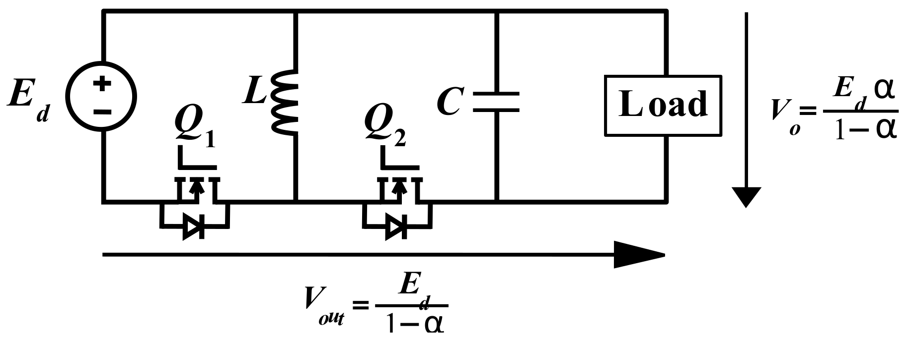
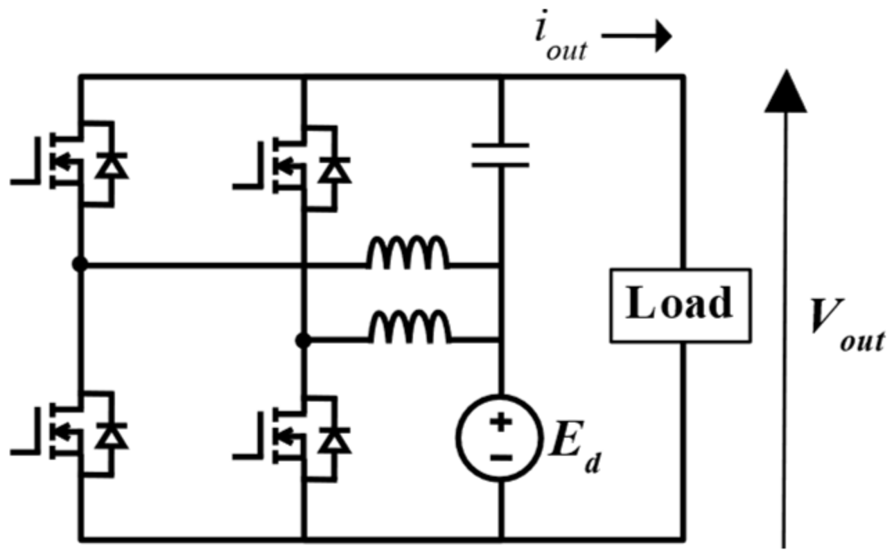
The proposed cells are modified buck–boost cells, which have been described in [43,44]. Figure 2 shows a conventional DC–DC buck–boost converter with terminal output voltage taken at the capacitor port (Vo), which has reversed polarity from the input side (Ed). In addition to the conventional output terminal Vo, another terminal (Vout) can be used for the load connection. If the load is connected to this terminal, then the converter can be redrawn as shown in Figure 3, in which the output voltage polarity is not reversed compared to the input Ed and has a common reference point. In ideal conditions and CCM, the average load voltage is
V o u t = E d + V o = E d 1 1 α
where Vout is the voltage in the new terminal, Vo is the voltage across the capacitors, Ed is the input voltage, and α is the duty cycle of switch Q1.
Note that (1) is the same as a conventional boost converter voltage gain. However, the rated voltage of filter capacitor C from the proposed converter is lower than the conventional boost DC–DC converter because it only has to withstand the difference between the output and input voltages and not the whole range of the output voltage. This advantage will lead to lower manufacturing costs. As it is derived from a buck–boost converter, the input and output currents are discontinuous. Therefore, an LC filter must be added to the input and/or output sides.
A modified buck–boost converter with an additional input LC filter can be seen in Figure 4. Normally, the filter inductor is placed between the input terminal and the energy transfer inductor L as shown in Figure 4a (Li and Ci). Without changing the characteristics, the filter inductor Li can also be placed at the bottom as shown in Figure 4b to obtain minimum losses. If the inductor Li is placed in the middle, as shown in Figure 4a, then a higher current will flow through the inductor (iL and id), resulting in greater losses. This position change removes a common reference point between the lower switch Q1 and input Ed, resulting in the need for an isolated gate driver circuit for Q1. However, this is considered not a serious tradeoff because the upper switch Q2 also requires an isolated driver, and both switches may share the same gate driving circuit design. Considering the voltage drops across switching devices and inductors in Figure 4b, the following equations can be obtained using state-space averaging,
V o u t = E d 1 α V Q α 1 α V D I o u t 1 α 2 R i α 2 + R L + R Q α + R D ( 1 α )
i d = α i L
where VQ and VD are voltage drops across transistors and diodes, Ri, RL, RQ, and RD are resistive components of the input filter inductor, energy transfer inductor, and switches, and id, iL, and Iout are the filter inductor, energy transfer inductor, and load currents.
With the same duty cycle and parameters for the inductors and capacitors, the modified buck–boost converter has a lower voltage drop compared to the conventional boost DC–DC converter with a difference in the resistive component of the input-filter inductor (Ri) with factor α2 [43]. As the voltage drop also represents conduction loss, conduction losses in input filters will be lower than the ones in conventional boost DC–DC converters. Compared to a conventional DC–DC boost converter with the same switching frequency, the switching losses are the same, and therefore, the efficiency of a modified buck–boost converter is higher [43].
For PV and battery converter applications, a low ripple current is desired. The multiphase technique can be applied to the modified buck–boost converter in Figure 3 to form the multiphase-modified buck–boost converter in Figure 5. Although Figure 5 shows only a two-phase modified buck–boost converter, it can also be made by more than two phases.

2.2. Modular Multilevel DC–DC Converter

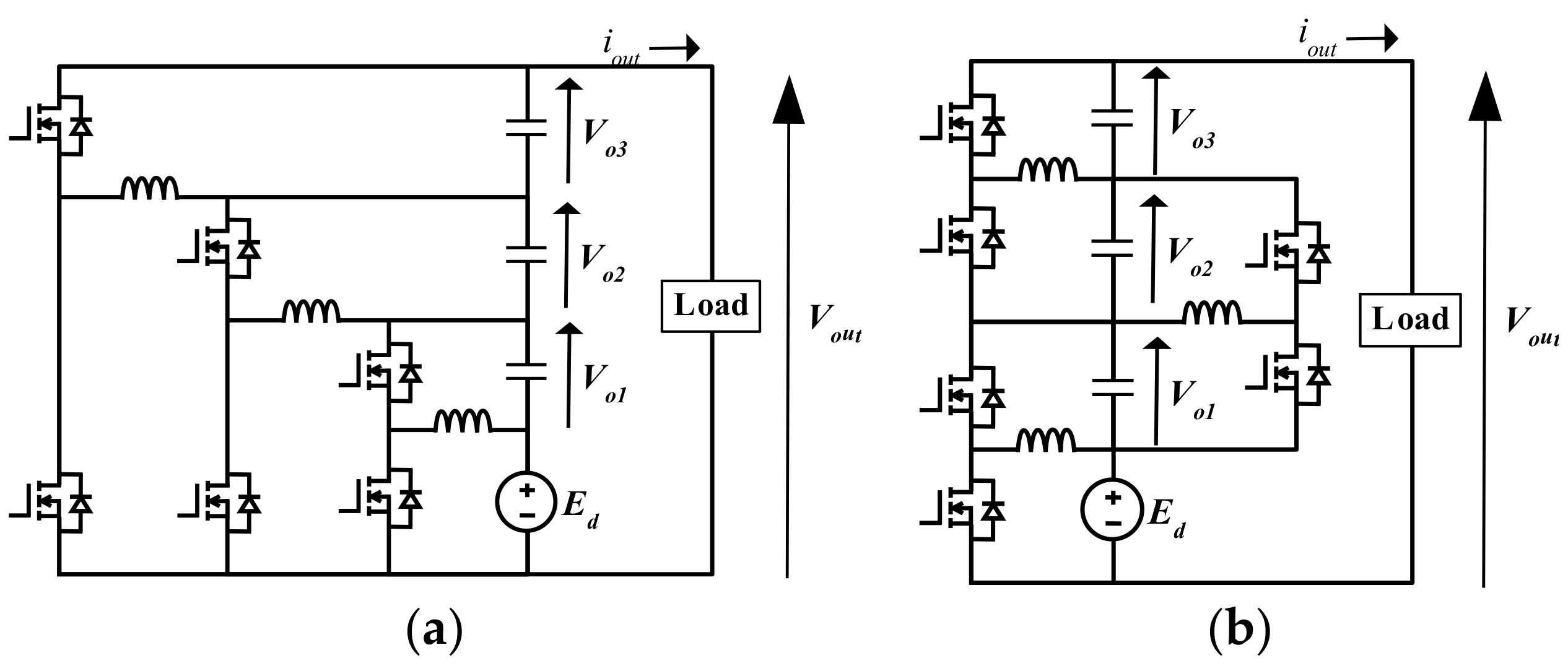
A modular multilevel assembly of several modified buck–boost converters is shown in Figure 6a. If the duty cycles of all converters are the same, then the total voltage ratio is given in (4), where N is the number of DC–DC converters. Though the voltage ratio can be very high, this system is not modular because the switches in each stage have different voltage-rating requirements. For example, the leftmost lower switch has to withstand Ed + Vo1 + Vo2 Volt, or 3Ed in the situation where the duty cycle of each cell is the same, whereas the upper switch only has to withstand Vo3 Volt, or equal to Ed.
V o u t E d = 1 1 α N
Cascading several buck–boost converters can also be completed as the one shown in Figure 6b. In this case, the voltage ratio is given in (5). This topology has been presented in [33] and it is called a “rainstick” topology. In this case, the modularity of each cell depends on the applied duty cycle [44]. Consider the bottommost cell consisting of DC source Ed, output voltage Vo1 across the capacitor in series with Ed, one inductor, and two switches. It is obvious from (1) that by using α = 0.5, Vo1 = Ed. The same principle also applies to the second cell consisting of Vo1 as the input/source and Vo2 as the output. Therefore, if all cells in the converter excluding either the first or the last cell are fixed at α = 0.5, they are modular and can be produced as simple plug-and-play blocks in which total output voltage can be raised according to the number of cells used. To manage the overall output voltage of the converter, only the first or the last cell needs to be controlled. This scheme simplifies the controller as there is only one cell that needs to be controlled.
V o u t E d = 1 + i = 1 N α i 1 α i
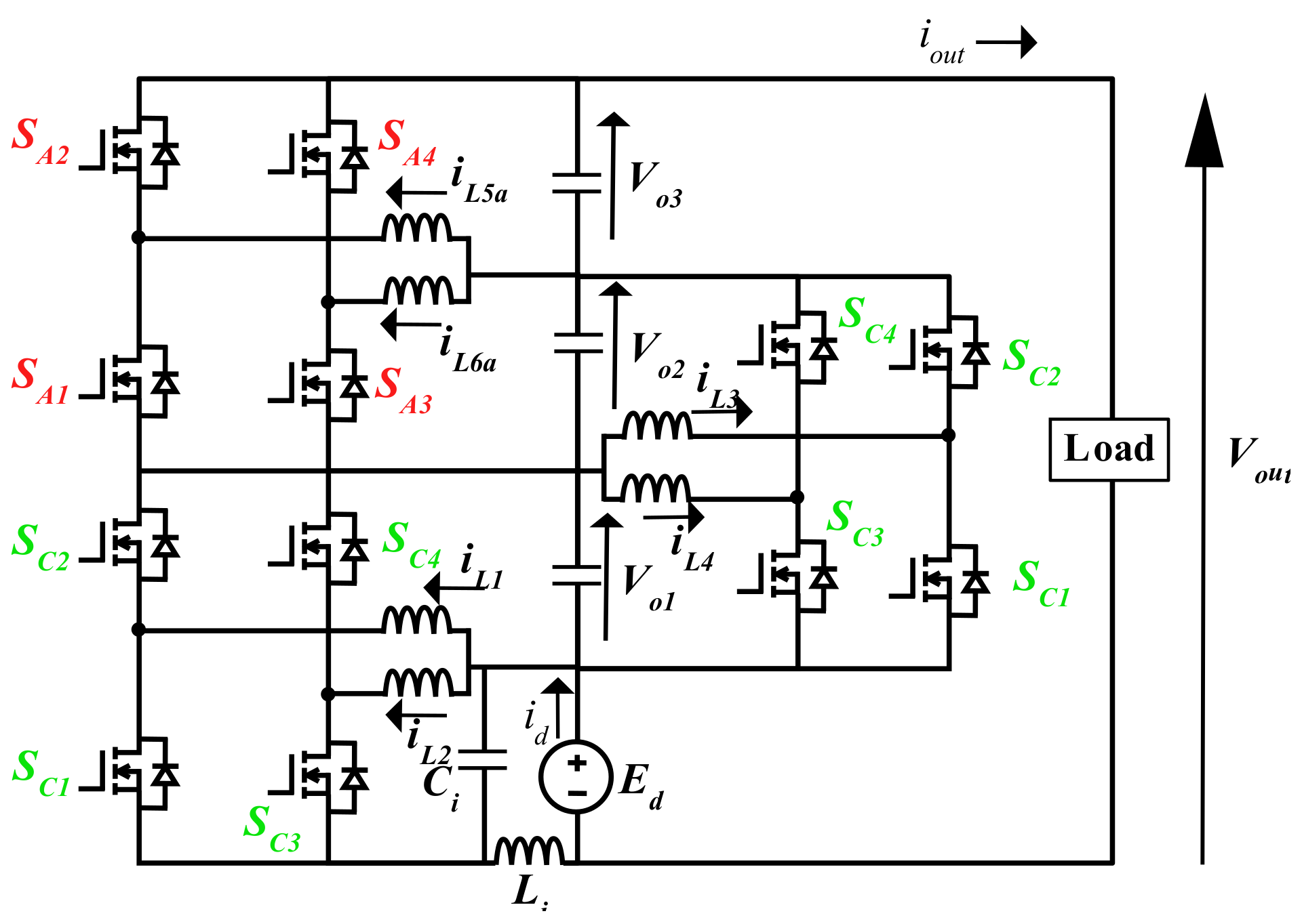
To reduce input ripple current, two-phase modified buck–boost cells can be used. A new two-phase modular multilevel DC–DC converter derived from a modified buck–boost converter with an input LC filter in the first cell is shown in Figure 7. The operational mode, ripple-current analysis, and output voltage of the proposed converter are described in the next section.

2.3. Operational Mode of Proposed Multilevel DC–DC Converter

The proposed MMC is operated by controlling only one cell, either the top (last) or the bottom (first) cell in Figure 7, and setting the duty cycle of the other cells to 0.5. In Figure 7, the topmost cell is controlled. SA indicates the switches whose duty cycle is adjusted/regulated, whilst SC indicates the switches with a constant half-duty cycle. S1S2 and S3S4 are complementary. When S1 and S3 are ON, S2 and S4 must be OFF and vice versa. In a multiphase configuration such as this, the pairs S1S2 and S3S4 are set to 180° phase difference so that the ripple current through their adjacent inductors cancels each other if seen from a source/input perspective.
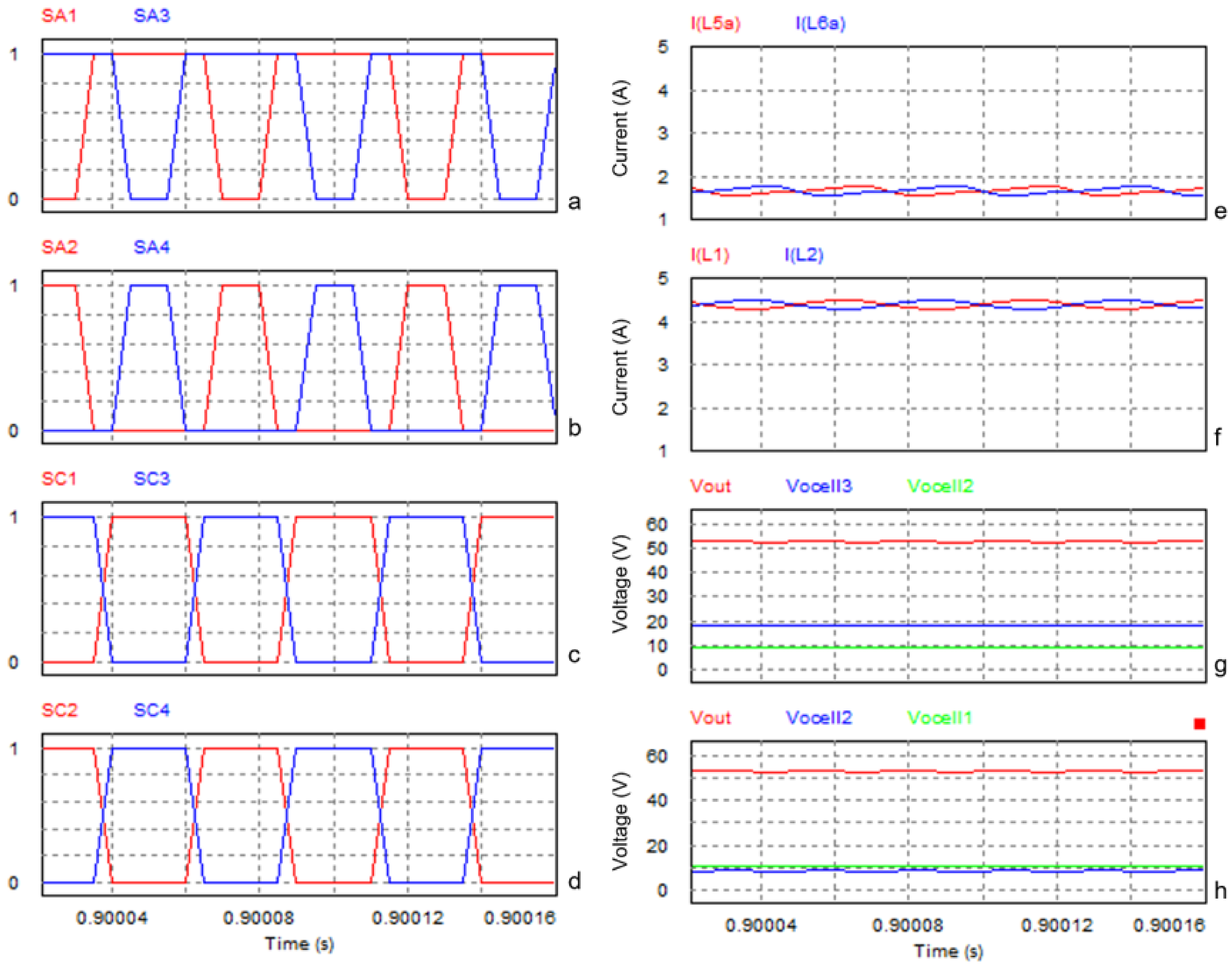
Figure 8a–d show the switching pattern for the converter in Figure 7. In this simulation, the duty cycle for the last cell (Figure 8a,b) is 0.7 whilst the others are 0.5. Other parameters for this simulation are provided in Table 1. The inductor currents (Figure 8e,f) are 180° displaced from each other, following their respective switching patterns. Figure 8g shows the voltage input and output for the adjusted cell. The input of this cell is the same as Ed due to the lower cells working on 2× voltage gain, whilst the output is adjusted by the duty cycle.

3. Ripple Current and Output Voltage Analysis

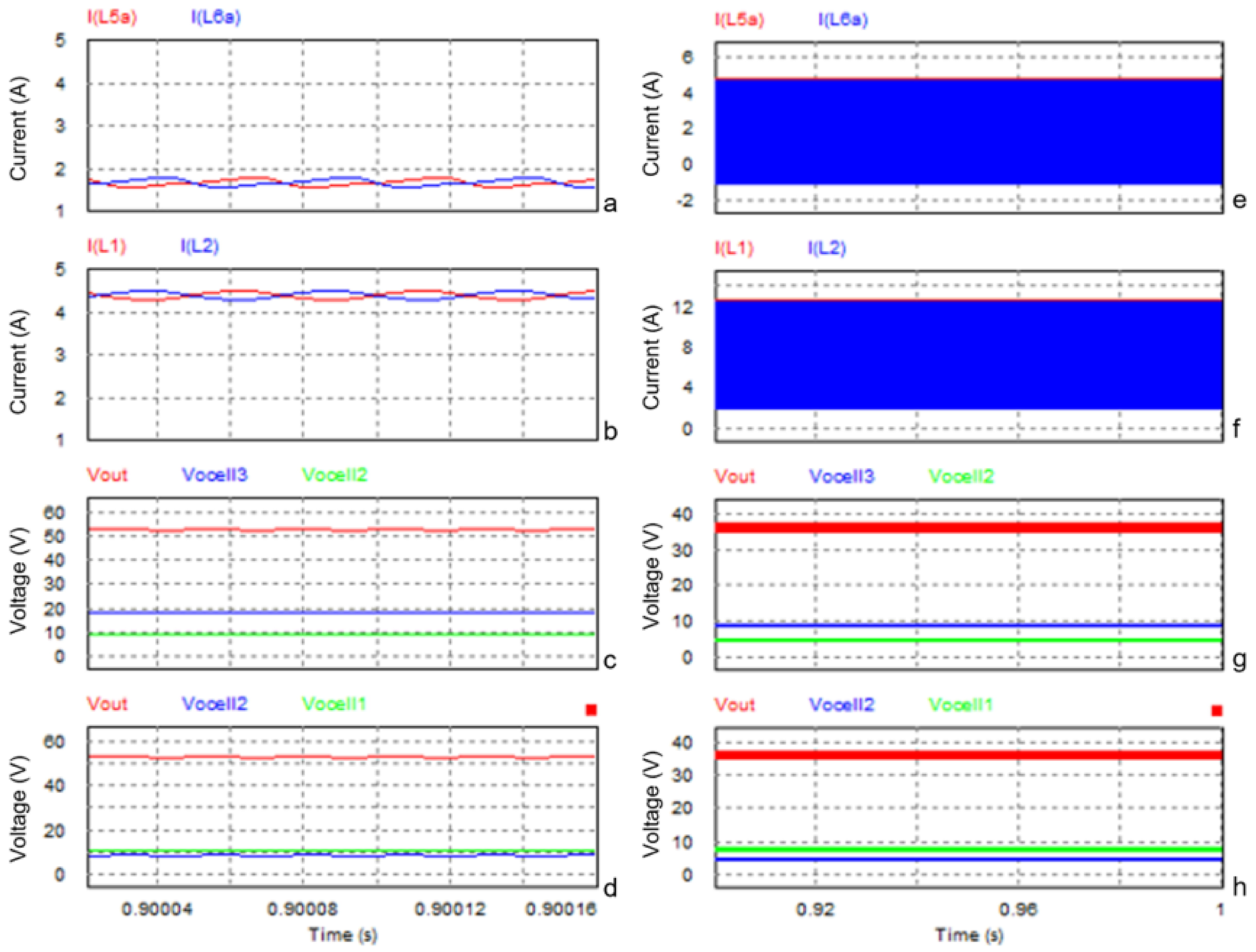
The analysis assumes that the converter runs in CCM to ensure boosting capability, and the DC source is assumed as a constant voltage source with no ripple, and the capacitor in each cell is assumed to be ideal with no ESR. CCM depends on the chosen inductance, switching frequency, duty cycle, and input current. Because the basic cell is based on a conventional buck–boost converter, the method for selecting component values and other parameters is the same, which has been explained in the literature, such as [45]. In DCM, due to the inductor current temporarily reaching 0, the converter will fail to boost voltage as shown in Figure 9. Figure 9a–d show the current and voltage waveforms in CCM for the same case as the one in Figure 8. Figure 9e–h shows the current and voltage waveforms for the same simulation, but the filter inductor is 20 µH. Aside from failing to boost voltage, the ripple current in each cell is also very high.

3.1. Ripple Current Analysis

Because if other than the first or the last cell of the proposed converter operates on a fixed half-duty cycle, it takes two phases to make the ripple become zero [46]. The ripple current of each cell will be the same because of modularity. Hence, in this section, the topology shown in Figure 5 is applied to analyze the ripple current based on [46]. The RMS value of the inductor ripple current is given in (6) and (7). The inductor ripple current of a single-phase modified buck–boost converter is the same as a conventional buck–boost DC–DC converter as written in (8).
I L ~ = K 2 α 1 α 2 3 f s α 1 ; f o r   0 α 0.5
I L ~ = K 2 α 1 2 3 f s ; f o r   0.5 α 1
I L ~ = E d α L 2 3 f s
where K = E d L + M , L is the self-inductance, M is the mutual inductance between the two inductors, and fs is the switching frequency.
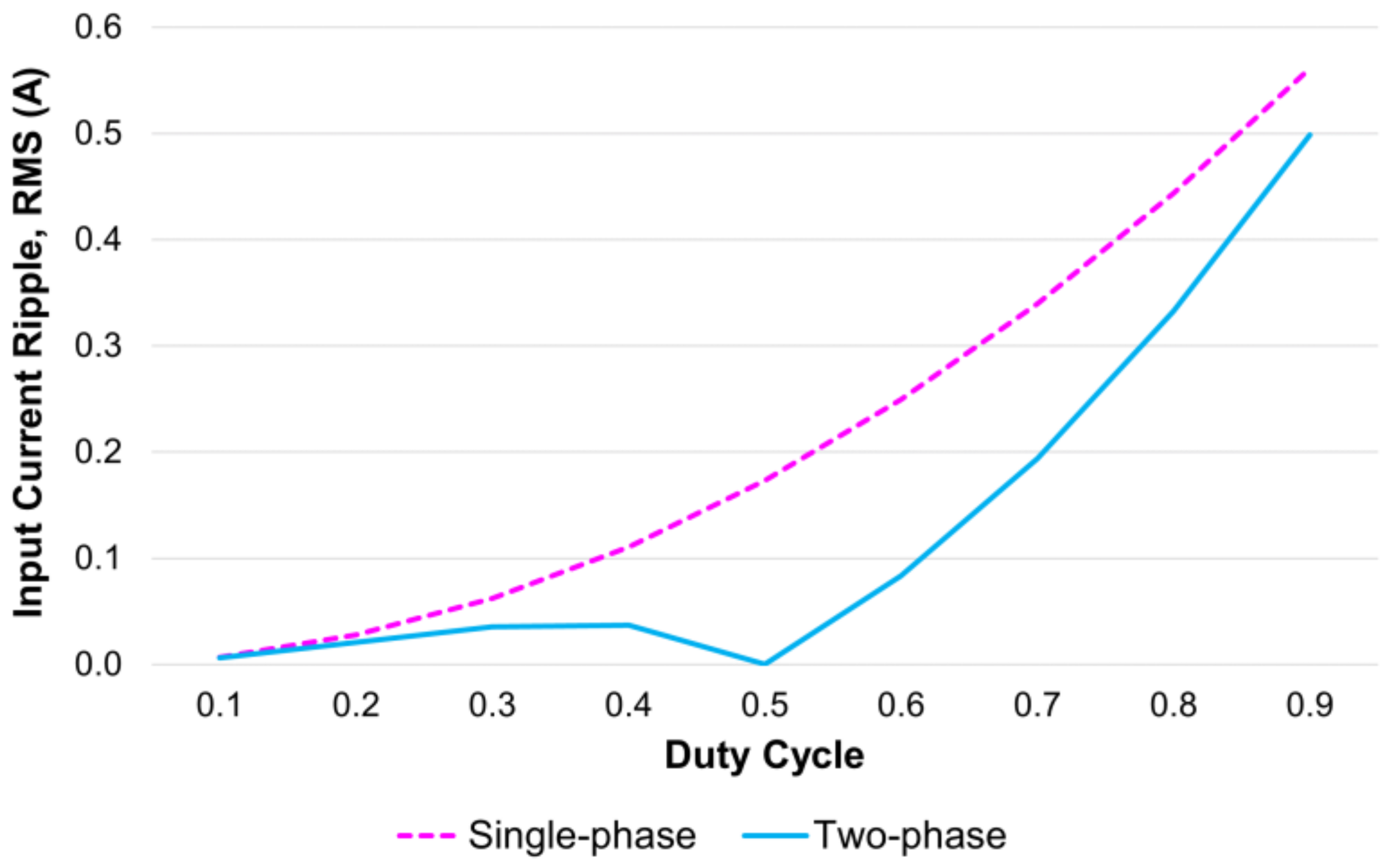
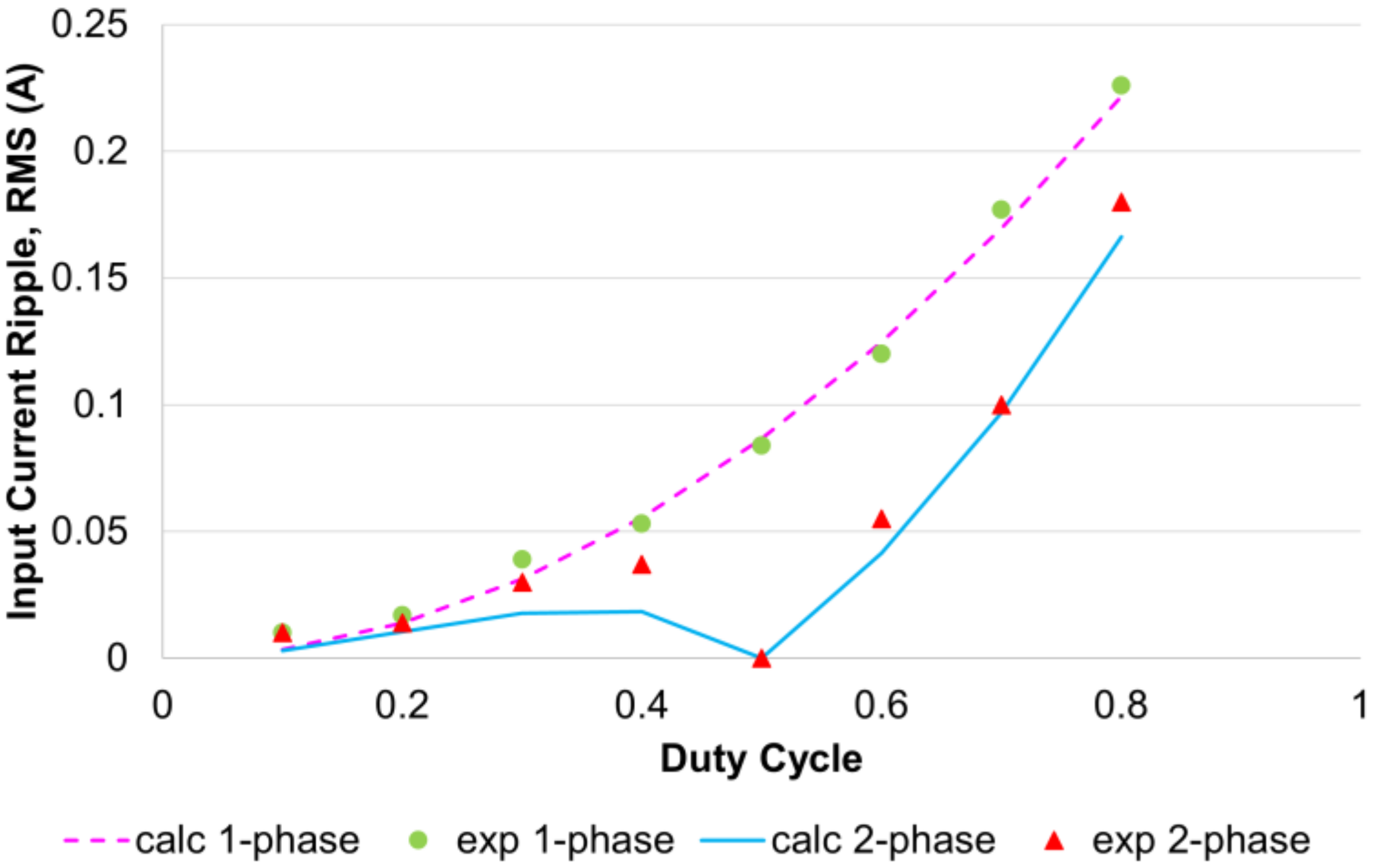
If the converter is input LC-filtered, then the inductor ripple current can be obtained by substituting (6), (7), and (8) to (3) and considering only the ripple components. The RMS value of the input currents in two-phase is given in (9) and (10), and for single-phase, it is given in (11). Figure 10 shows the comparison of the inductor ripple current between single-phase and two-phase modified buck–boost DC–DC converters. The parameters for this calculation are as follows: Ed = 48 VDC, L = 1 mH with no mutual inductance, and fs = 20 kHz. The ripple content is generally lower in a two-phase converter compared to a single-phase; however, special attention must be paid when α = 0.5. By using two phases, the ripple current can theoretically be eliminated. This implies that the two-phase configuration of the proposed converter is highly suitable for low ripple-current requirements such as battery chargers/dischargers and PV converters.
I d ~ = K 2 α 1 α 2 2 3 f s α 1 ; f o r   0 α 0.5
I d ~ = K 2 α 1 α 2 3 f s ; f o r   0.5 α 1
I d ~ = E d α 2 L 2 3 f s

3.2. Output Voltage Analysis

The proposed converter in Figure 7 can be extended until N-levels achieve the output voltage as described in (12). Because the input of the next cell is taken at the output terminal of the previous cell, the output voltage of each cell can be calculated as a conventional buck–boost converter, but the polarity is not reversed as given in (13), with an Ri value of 0 for cells other than the first one. Equation (13) is used to derive the output-voltage equation of the proposed converter. The output voltage of the modular 3-level modified buck–boost DC–DC converter in Figure 7 is given in (14). Controlling the duty cycle of the first and the last cell has a different impact on the output voltage gain.
V o u t , N - l e v e l s = E d + V o 1 + V o 2 + V o 3 + + V o N
V o , e a c h c e l l = E d   α 1 α V Q α 1 α V D I o u t 1 α 2 R i α 2 + R L + R Q α + R D ( 1 α )
V o u t , 3 - l e v e l s = E d + V o 1 + V o 2 + V o 3

3.2.1. Controlling the First Cell

Controlling the first cell means the duty cycle of the first cell is varied while the duty cycle of other cells is maintained at 0.5. The voltage gain equation for Vo1 is given in (15).
V o 1 = E d α 1 α V Q α 1 α V D I o u t , 1 1 α 2 R i α 2 + R L + R Q α + R D ( 1 α )
Substituting α = 0.5 and Ri = 0 to (15), the output voltage of the second cell can be obtained as follows:
V o 2 = V o 1 V Q V D X I o u t , 2
with
X = R L + 0.5   R Q + 0.5   R D 0.25 .
For the third cell, the output voltage is given in (19). By substituting (16) and (19) to (14), the output voltage for the 3-level converter is given in (21).
V o 3 = V o 2 V Q V D X I o u t , 3
V o 3 = V o 1 2 V Q + V D X I o u t , 2 X I o u t , 3
V o u t , 3 - l e v e l s = E d + V o 1 + V o 1 V Q V D X I o u t , 2 + V o 1 2 V Q + V D X I o u t , 2 X I o u t , 3
V o u t , 3 - l e v e l s = E d + 3 V o 1 3 V Q + V D 2 X I o u t , 2 X I o u t , 3
By using the same method for 3 levels, the output voltage of 4 levels and 5 levels can be obtained as follows:
V o u t , 4 - l e v e l s = E d + 4 V o 1 6 V Q + V D 3 X I o u t , 2 2 X I o u t , 3 X I o u t , 4
V o u t , 5 - l e v e l s = E d + 5 V o 1 10 V Q + V D 4 X I o u t , 2 3 X I o u t , 3 2 X I o u t , 4 X I o u t , 5
with
I o u t , 2   u n t i l   N = I o u t
I o u t , 1 = α 1 α I o u t , 2 = α 1 α I o u t
From (21)–(23), the general form of the total output voltage gained from controlling the first cell is given in (26). If the components are ideal, then the terms that depend on the components’ nonideality, such as voltage drop across the switches (VQ and VD) and internal resistance (RQ, RD, et cetera), are equal to 0. The voltage gain of the converter with a controlled first cell can then be given in (27).
V o u t , N - l e v e l s = E d 1 + N 1 α 1 α V Q N N 1 2 + N α 1 α V D N N 1 2 + N I o u t [ R i N α 3 1 α 3 + R L N α 1 α 3 + 2 N N 1 + R Q N α 2 1 α 3 + N N 1 + R D N α 1 α 2 + N N 1 ]
M f i r s t = 1 + N 1 α 1 α

3.2.2. Controlling the Last Cell

The voltage gain for the last-cell-controlled converter can be derived the same way as controlling the first cell, with the duty cycle for the last cell now being varied and the others fixed at 0.5. For the converter shown in Figure 7, the output voltage of the first and second cells can be calculated by using (28) and (29) respectively. The output voltage for the third (last) cell takes into account the varying duty cycle and is given in (30). By changing (28)–(30) to (14) and grouping each component, the 3-level total output voltage gain is given in (31). Equations (32) and (33) give the total output voltage gain for 4-level and 5-level converters. Lastly, (34) gives the general form of the n-level last-cell-controlled modified buck–boost converter. Similar to the previous section, if the components are ideal, then (34) can be rewritten as (35).
V o 1 = E d V Q V D ( X + R i ) I o u t , 1
V o 2 = E d 2 V Q + V D ( X + R i ) I o u t , 1 X I o u t , 2
V o 3 = V o 2 α 1 α V Q α 1 α V D I o u t , 3 1 α 2 R L + R Q α + R D ( 1 α )
V o u t , 3 - l e v e l s = E d 3 2 α 1 α V Q 3 + 3 α 1 α V D 3 + 1 + α 1 α I o u t X 3 α 1 α 2 + R i 2 α 1 α + R L + R Q α + R D ( 1 α ) 1 α 2
V o u t , 4 - l e v e l s = E d 4 3 α 1 α V Q 6 + 4 α 1 α V D 6 + 1 + 2 α 1 α I o u t X 6 α 3 α 2 1 α 2 + R i 3 2 α 1 α + R L + R Q α + R D ( 1 α ) 1 α 2
V o u t , 5 - l e v e l s = E d 5 4 α 1 α V Q 10 + 5 α 1 α V D 10 + 1 + 3 α 1 α I o u t X 10 α 6 α 2 1 α 2 + R i 4 3 α 1 α + R L + R Q α + R D ( 1 α ) 1 α 2
V o u t , N - l e v e l s = E d N N 1 α 1 α V Q N N 1 2 + N α 1 α V D N N 1 2 + N 2 α + 1 1 α I o u t [ R i N 1 N 2 α 1 α + R L 4 α i = 1 N 1 i i 1 α + 1 1 α 2 + R Q 2 α i = 1 N 1 i i 1 α + α 1 α 2 + R D 2 α i = 1 N 1 i i 1 α + 1 α 1 α 2 ]
M l a s t = N N 1 α 1 α
Figure 11 shows the trend of the voltage conversion ratio against the duty cycle for (27) and (35). Adjusting the duty cycle in the first cell will result in a wider voltage conversion ratio than adjusting the last cell. However, adjusting the duty cycle of the last cell will have zero input ripple current because the first cell is maintained at half duty cycle as shown in Figure 10.

3.3. Comparison with Previous Topology

From Section 3.1 and Section 3.2, it can be seen that the proposed topology can achieve high voltage gain and zero ripple current theoretically; moreover, it has modular and bidirectional capability. Table 2 shows a comparison between the proposed topology and some of the previous topologies.

4. Experimental Results

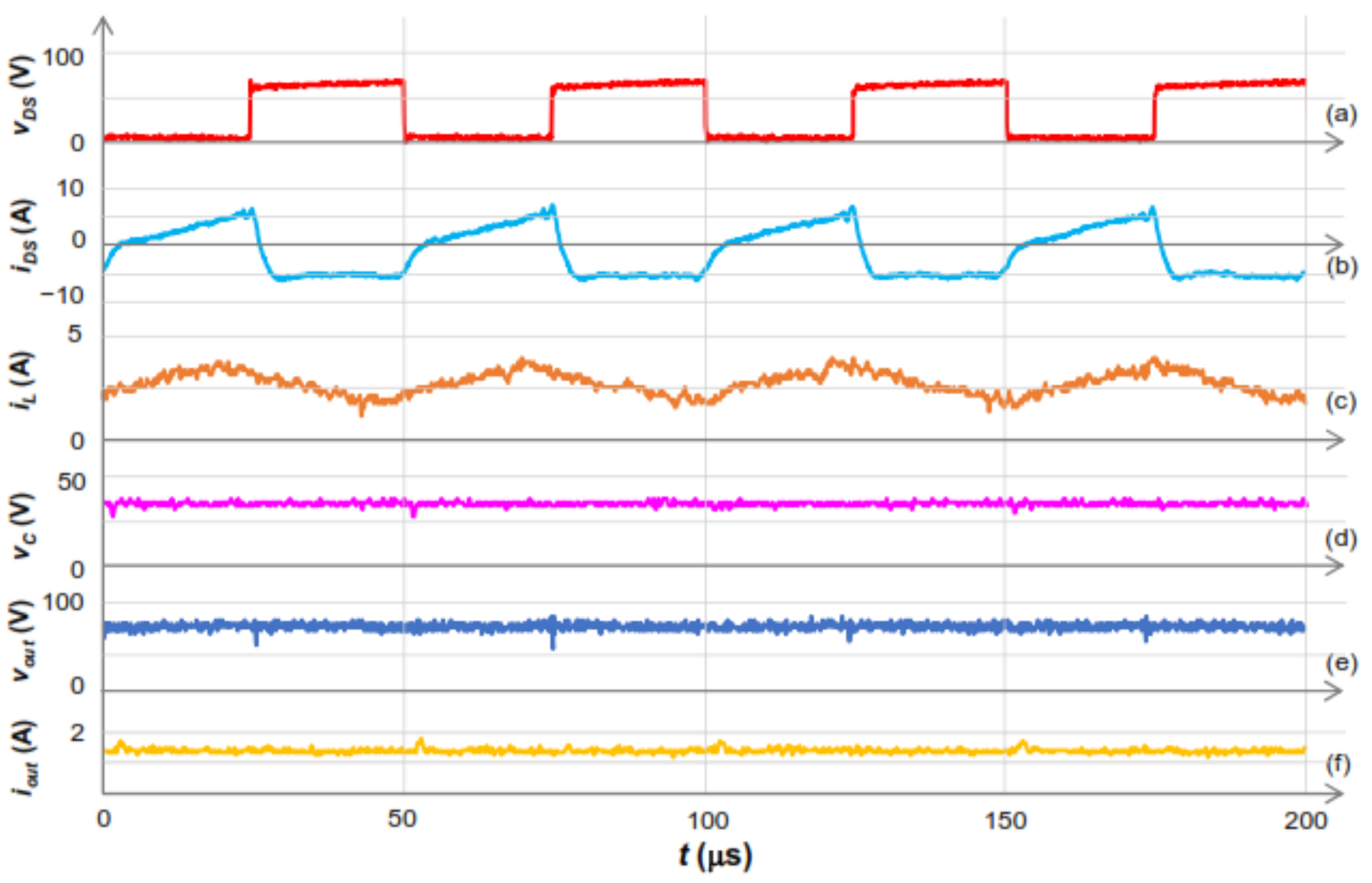
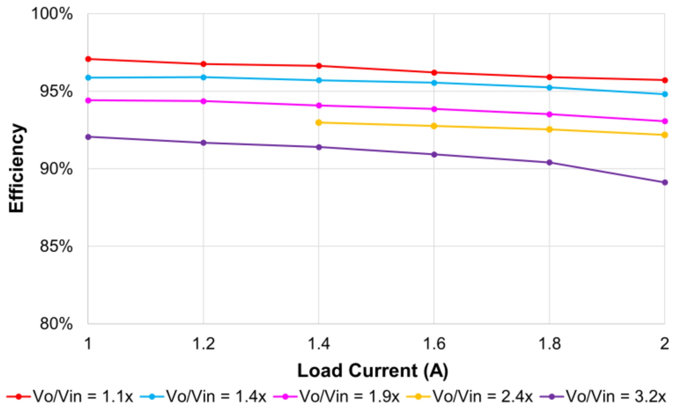
Verification of the proposed converter is completed first in single-level and second in multilevel configurations. Ref. [43] discusses the modified buck–boost topology derivation and single-level single-phase experiment. The results of this experiment show that the modified buck–boost topology has a lower voltage drop and conduction loss than the conventional boost DC–DC power converter, and its efficiency is higher in lower duty cycles. The results are also included in this paper for completion. Figure 12 shows the current and voltage waveforms across the inductor, capacitor, and switches for the single-phase experiment. With a 36 V input and half-duty cycle, the voltage across the output capacitor is also 36 V (Figure 12d), resulting in the total output of this single-cell modified buck–boost converter being 72 V (Figure 12e). Figure 12c shows the current through inductor L in single-phase mode. The inductor L ripple-current content in this experiment is 30.79%. The efficiency of this converter for several duty cycles/voltage gain overload current variations is shown in Figure 13. It has also been demonstrated that the converter can operate bidirectionally. The experiments in this paper focus on verifying the ripple-current analysis and voltage-conversion analysis as a multilevel converter.

4.1. Ripple Current Verification

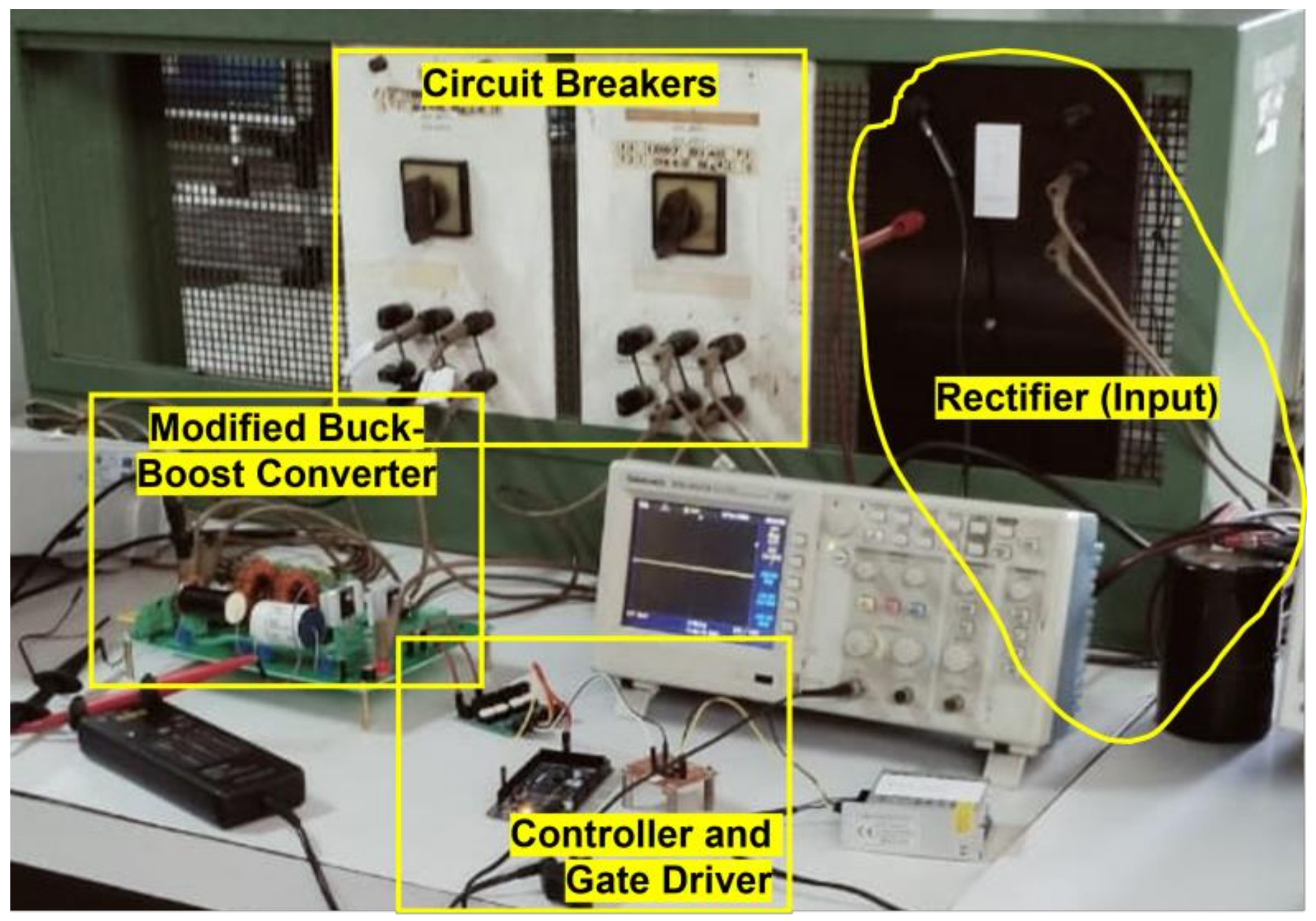
The purpose of this experiment is to measure the amount of input ripple current of one modified buck–boost cell both as single-phase and two-phase. Figure 14 shows the experiment setup. The DC voltage source is obtained from a rectified single-phase AC voltage and filtered with a 5-mF capacitor. The parameters for this experiment are listed in Table 3. The two-phase experiment uses the same parameters but without mutual inductance between the phases.
The comparison between inductor ripple current in single-phase and two-phase mode is shown in Figure 15. The RMS of the inductor ripple current from a single-phase modified buck–boost converter is compared to the two-phase one (both as discrete points) and superimposed on the calculated ripple-current values from Figure 10. It can be seen that the experimental results agree with the calculation with minimal discrepancy. This experiment also shows that with two phases, a half-duty cycle effectively eliminates the ripple current. Other parameters that affect ripple currents, as described by (9)–(11), are input voltage, switching frequency, and inductance. These parameters can be adjusted for optimal values, especially in the single-phase configuration, depending on the power rating of the target design. However, in a two-phase configuration, fixing the duty cycle at 0.5 is the most effective way to minimize ripple current and implicitly gives more freedom in choosing switching frequency and inductor values to meet any specific requirement.
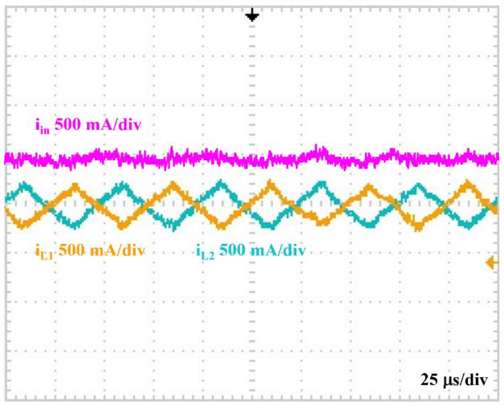
Zero ripple currents occur due to the ripple cancellation of inductor currents. Figure 16 shows inductor currents for the two-phase experiment. The switching pattern is displaced by 180° between phase 1 and phase 2 so that at half-duty cycle, the maxima of phase 1 coincides with the minima of phase 2. Seen from the source (which in practice may be a PV panel or a battery), the resultant ripple is 0. Due to nonidealities in real components, computational delay, signal delay, and other parasitic factors, it is nearly impossible to guarantee that currents in both phases perfectly cancel each other. Thus, a very small ripple current may still appear, as evident in Figure 16. For this experiment, the ripple content from the source perspective is less than 5% of the total current.

4.2. Output Voltage Verification

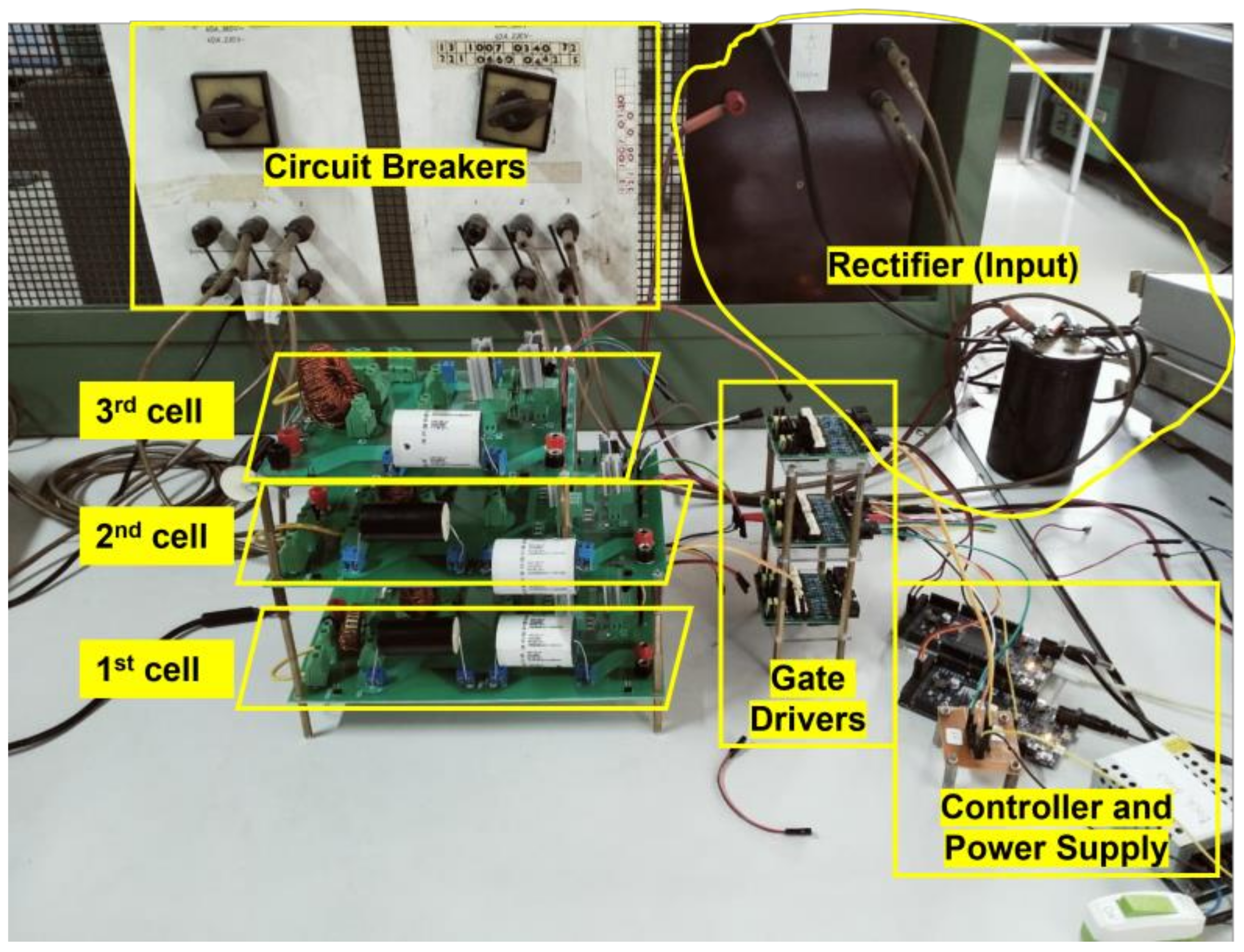
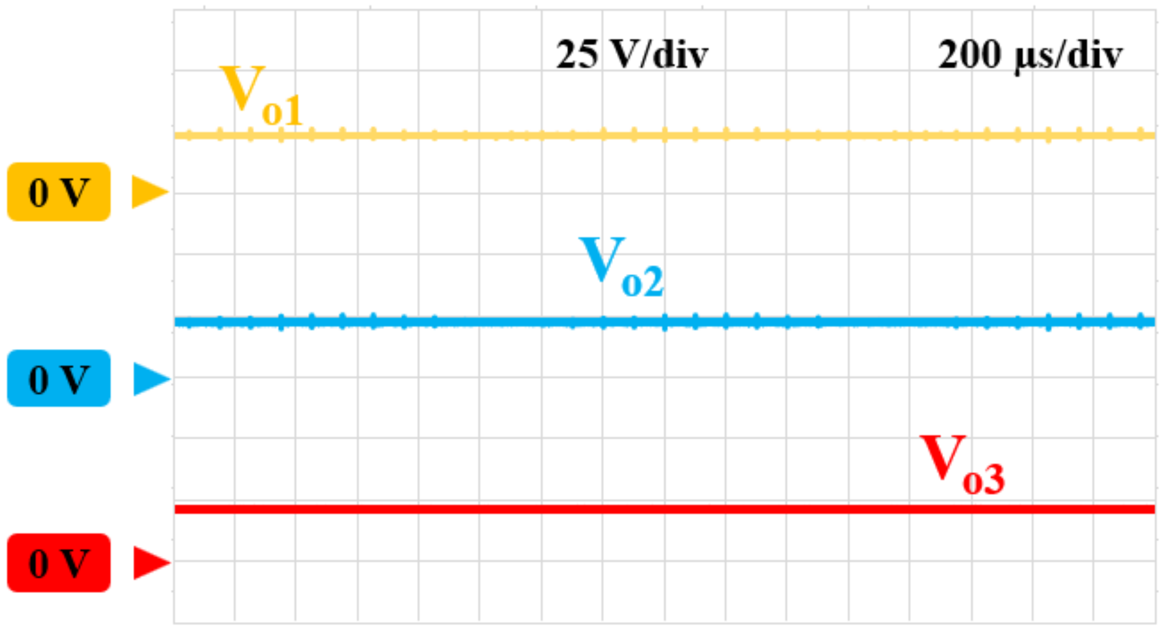
This experiment uses the same parameters from Table 3. Three cells are used with a slight difference in the third cell due to assembly error, as shown in the experiment setup in Figure 17. The duty cycle for all cells is fixed at 0.5, and the voltage is measured at the output capacitor in series with the input terminal of each cell (capacitor C in Figure 4). The result is shown in Figure 18. The converter is in a bare-bones open-loop control scheme, meaning neither a feedback loop nor an additional control method is applied. The output voltage of each cell is approximately the same as input Ed (with the exception of the voltage output of the third cell due to the aforementioned issue), proving the claim that this converter does not need voltage balancing. The total voltage gain of this converter matches (27) (as well as (35) because, at a = 0.5, the two controlling methods have the same voltage conversion ratio).
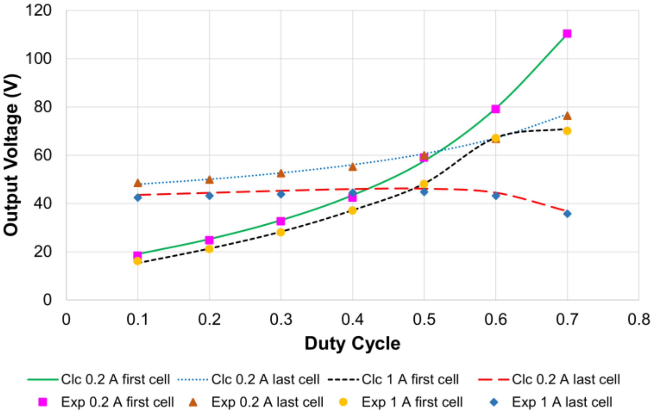
Other than verifying the voltage ratio of the MMC version of the proposed converter, this experiment also compares the voltage output gained by controlling the first and the last cell, each in two different load conditions, and also compares them with calculations. Due to the current carrying capacity of the prototype, the input voltage for this experiment is reduced to 15 V. This experiment does not involve transient load conditions as it is more focused on verifying the differences in applying the control method for MMC configuration.
In Figure 19, the dotted, dashed, and solid lines show the calculation results, while the markers show the experimental measurement results. In accordance with previous analyses, at the same load conditions, the curves corresponding to first-cell-controlled and last-cell-controlled converters intersect at a half-duty cycle. Due to employing bare-bones open loop control, there is no output voltage regulation; therefore, with higher load currents, the voltages naturally drop.

5. Conclusions

This paper proposes a modular multilevel DC–DC converter with low cost, high efficiency, and a high voltage conversion ratio that is derived from a modified buck–boost DC–DC converter. The modified buck–boost cell has the same voltage gain characteristics as a simple boost converter. The output terminal polarity is unreversed with respect to the input terminal, and the inductor within provides embedded filtering of current and voltage ripples. By using the multileveling scheme described in this paper, the modularity of the cells is maintained and no additional voltage-balancing techniques are needed.
The proposed MMC is suitable for various applications that require a very high voltage conversion ratio. It is especially suitable for interfacing PV panels and batteries to a DC microgrid bus that may be a magnitude higher in voltage. The simplicity of stacking the basic cells into a multilevel converter offers ease of assembly and control that is highly important for implementation in remote areas. For applications that hinge on very low ripple currents, multiphase configuration of the basic cell is a reliable option with a minimal drawback in overall footprint (due to the additional component) and cost.
The proposed converter still has room for exploration. This paper presents proof of concept of the basic cell and multileveling scheme by means of a downscaled prototype with promising results. Real-scale testing and closed-loop control are left for the next research. Optimization methods on the number of levels and phases for specific uses are also a potential topic for future work.

Author Contributions

Conceptualization, P.A.D.; methodology, R.D.N.A., A.R. and P.A.D.; software, R.D.N.A. and N.R.; validation, T.A., J.F., A.R. and P.A.D.; formal analysis, R.D.N.A.; investigation, R.D.N.A. and N.R.; resources, R.D.N.A. and N.R.; data curation, R.D.N.A.; writing—original draft preparation, R.D.N.A.; writing—review and editing, R.D.N.A., T.A., J.F., A.R. and P.A.D.; visualization, R.D.N.A.; supervision, A.R. and P.A.D.; project administration, R.D.N.A.; funding acquisition, A.R. and P.A.D. All authors have read and agreed to the published version of the manuscript.

Funding

This research was partially funded by Korea Midland Power Company, Institut Teknologi Bandung (Grant no. 223/IT1.B07.1/TA.00/2022), and the School of Electrical Engineering and Informatics, Institut Teknologi Bandung.

Data Availability Statement

Not applicable.

Acknowledgments

The authors would like to thank all of the PAD Research Group members who assisted during the experiments and provided valuable discussion.

Conflicts of Interest

The authors declare no conflict of interest.

Nomenclature

CCMContinuous conduction mode
DCMDiscontinuous conduction mode
ESREquivalent series resistance
EVElectric Vehicle
HVDCHigh Voltage DC
PCBPrinted circuit board
PVPhotovoltaic
RMSRoot mean square

References

  1. Debnath, D.; Chatterjee, K. Two-Stage Solar Photovoltaic-Based Stand-Alone Scheme Having Battery as Energy Storage Element for Rural Deployment. IEEE Trans. Ind. Electron. 2015, 62, 4148–4157. [Google Scholar] [CrossRef]
  2. Wu, H.; Sun, K.; Chen, L.; Zhu, L.; Xing, Y. High Step-Up/Step-Down Soft-Switching Bidirectional DC–DC Converter with Coupled-Inductor and Voltage Matching Control for Energy Storage Systems. IEEE Trans. Ind. Electron. 2016, 63, 2892–2903. [Google Scholar] [CrossRef]
  3. Mahmood, A.; Zaid, M.; Ahmad, J.; Khan, M.A.; Khan, S.; Sifat, Z.; Lin, C.-H.; Sarwar, A.; Tariq, M.; Alamri, B. A Non-Inverting High Gain DC–DC Converter with Continuous Input Current. IEEE Access 2021, 9, 54710–54721. [Google Scholar] [CrossRef]
  4. Kim, J.; Kwon, I. Design of a High-Efficiency DC–DC Boost Converter for RF Energy Harvesting IoT Sensors. Sensors 2022, 22, 10007. [Google Scholar] [CrossRef] [PubMed]
  5. Sharma, R.; Gao, H. Low cost high efficiency DC–DC converter for fuel cell powered auxiliary power unit of a heavy vehicle. IEEE Trans. Power Electron. 2006, 21, 587–591. [Google Scholar] [CrossRef]
  6. Yang, J.; He, Z.; Pang, H.; Tang, G. The Hybrid-Cascaded DC–DC Converters Suitable for HVdc Applications. IEEE Trans. Power Electron. 2015, 30, 5358–5363. [Google Scholar] [CrossRef]
  7. Gontijo, G.F.; Wang, S.; Kerekes, T.; Teodorescu, R. Novel Converter Topology With Reduced Cost, Size and Weight for High-Power Medium-Voltage Machine Drives: 3x3 Modular Multilevel Series Converter. IEEE Access 2021, 9, 49082–49097. [Google Scholar] [CrossRef]
  8. Askarian, I.; Pahlevani, M.; Knight, A.M. Three-Port Bidirectional DC/DC Converter for DC Nanogrids. IEEE Trans. Power Electron. 2021, 36, 8000–8011. [Google Scholar] [CrossRef]
  9. Palumbo, G.; Pappalardo, D. Charge Pump Circuits: An Overview on Design Strategies and Topologies. IEEE Circuits Syst. Mag. 2010, 10, 31–45. [Google Scholar] [CrossRef]
  10. Li, S.; Zheng, Y.; Wu, B.; Smedley, K.M. A Family of Resonant Two-Switch Boosting Switched-Capacitor Converter with ZVS Operation and a Wide Line Regulation Range. IEEE Trans. Power Electron. 2018, 33, 448–459. [Google Scholar] [CrossRef]
  11. Qian, W.; Cao, D.; Cintron-Rivera, J.G.; Gebben, M.; Wey, D.; Peng, F.Z. A Switched-Capacitor DC–DC Converter with High Voltage Gain and Reduced Component Rating and Count. IEEE Trans. Ind. Appl. 2012, 48, 1397–1406. [Google Scholar] [CrossRef]
  12. Li, S.; Xie, W.; Smedley, K.M. A Family of an Automatic Interleaved Dickson Switched-Capacitor Converter and Its ZVS Resonant Configuration. IEEE Trans. Ind. Electron. 2019, 66, 255–264. [Google Scholar] [CrossRef]
  13. Xie, H.; Li, R. A Novel Switched-Capacitor Converter with High Voltage Gain. IEEE Access 2019, 7, 107831–107844. [Google Scholar] [CrossRef]
  14. Nguyen, M.-K.; Duong, T.-D.; Lim, Y.-C. Switched-Capacitor-Based Dual-Switch High-Boost DC–DC Converter. IEEE Trans. Power Electron. 2018, 33, 4181–4189. [Google Scholar] [CrossRef]
  15. Fardahar, S.M.; Sabahi, M. New Expandable Switched-Capacitor/Switched-Inductor High-Voltage Conversion Ratio Bidirectional DC–DC Converter. IEEE Trans. Power Electron. 2020, 35, 2480–2487. [Google Scholar] [CrossRef]
  16. Forouzesh, M.; Siwakoti, Y.P.; Gorji, S.A.; Blaabjerg, F.; Lehman, B. Step-Up DC–DC Converters: A Comprehensive Review of Voltage-Boosting Techniques, Topologies, and Applications. IEEE Trans. Power Electron. 2017, 32, 9143–9178. [Google Scholar] [CrossRef]
  17. Prudente, M.; Pfitscher, L.L.; Emmendoerfer, G.; Romaneli, E.F.; Gules, R. Voltage Multiplier Cells Applied to Non-Isolated DC–DC Converters. IEEE Trans. Power Electron. 2008, 23, 871–887. [Google Scholar] [CrossRef]
  18. Meraj, M.; Bhaskar, M.S.; Iqbal, A.; Al-Emadi, N.; Rahman, S. Interleaved Multilevel Boost Converter with Minimal Voltage Multiplier Components for High-Voltage Step-Up Applications. IEEE Trans. Power Electron. 2020, 35, 12816–12833. [Google Scholar] [CrossRef]
  19. Azizkandi, M.E.; Sedaghati, F.; Shayeghi, H.; Blaabjerg, F. A High Voltage Gain DC–DC Converter Based on Three Winding Coupled Inductor and Voltage Multiplier Cell. IEEE Trans. Power Electron. 2020, 35, 4558–4567. [Google Scholar] [CrossRef]
  20. Barreto, L.H.S.C.; Praca, P.P.; Henn, G.A.L.; Silva, R.N.A.L.; Oliveira, D.S. Single stage high voltage gain boost converter with voltage Multiplier Cells for battery charging using photovoltaic panels. In Proceedings of the 2012 Twenty-Seventh Annual IEEE Applied Power Electronics Conference and Exposition (APEC), Orlando, FL, USA, 5–9 February 2012; pp. 364–368. [Google Scholar] [CrossRef]
  21. Tofoli, F.L.; De Souza Oliveira, S.; Torrico-Bascopé, R.P.; Alcazar, Y.J.A. Novel Nonisolated High-Voltage Gain DC–DC Converters Based on 3SSC and VMC. IEEE Trans. Power Electron. 2012, 27, 3897–3907. [Google Scholar] [CrossRef]
  22. Zhu, B.; Wei, Z.; Chen, Y.; Wang, H.; Vilathgamuwa, D.M. Multiple Input-Terminal Voltage Multiplier Circuit. IEEE Trans. Ind. Appl. 2020, 56, 5075–5082. [Google Scholar] [CrossRef]
  23. Park, K.-B.; Moon, G.-W.; Youn, M.-J. Nonisolated High Step-Up Stacked Converter Based on Boost-Integrated Isolated Converter. IEEE Trans. Power Electron. 2011, 26, 577–587. [Google Scholar] [CrossRef]
  24. Lu, Y.; Liu, H.; Hu, H.; Wu, H.; Xing, Y. Single-switch high step-up converter with coupled-inductor and built-in transformer. In Proceedings of the 2015 IEEE 10th Conference on Industrial Electronics and Applications (ICIEA), Auckland, New Zealand, 15–17 June 2015; pp. 1181–1186. [Google Scholar] [CrossRef]
  25. Li, F.; Liu, H. A Cascaded Coupled Inductor-Reverse High Step-Up Converter Integrating Three-Winding Coupled Inductor and Diode–Capacitor Technique. IEEE Trans. Ind. Informatics 2017, 13, 1121–1130. [Google Scholar] [CrossRef]
  26. Wu, H.; Lu, J.; Shi, W.; Xing, Y. Nonisolated Bidirectional DC–DC Converters with Negative-Coupled Inductor. IEEE Trans. Power Electron. 2012, 27, 2231–2235. [Google Scholar] [CrossRef]
  27. Chen, S.-M.; Lao, M.-L.; Hsieh, Y.-H.; Liang, T.-J.; Chen, K.-H. A Novel Switched-Coupled-Inductor DC–DC Step-Up Converter and Its Derivatives. IEEE Trans. Ind. Appl. 2015, 51, 309–314. [Google Scholar] [CrossRef]
  28. Liu, H.; Hu, H.; Wu, H.; Xing, Y.; Batarseh, I. Overview of High-Step-Up Coupled-Inductor Boost Converters. IEEE J. Emerg. Sel. Top. Power Electron. 2016, 4, 689–704. [Google Scholar] [CrossRef]
  29. Chen, S.-M.; Liang, T.-J.; Yang, L.-S.; Chen, J.-F. A Cascaded High Step-Up DC–DC Converter with Single Switch for Microsource Applications. IEEE Trans. Power Electron. 2011, 26, 1146–1153. [Google Scholar] [CrossRef]
  30. Sulthon, M.; Damanik, O.A.; Efraim; Rizqiawan, A.; Dahono, P.A. A new simplified cascaded boost converter for high ratio and low ripple application. In Proceedings of the 2017 4th International Conference on Electric Vehicular Technology (ICEVT), Bali, Indonesia, 2–5 October 2017; pp. 117–124. [Google Scholar] [CrossRef]
  31. Ai, J.; Lin, M.; Yin, M. A Family of High Step-Up Cascade DC–DC Converters with Clamped Circuits. IEEE Trans. Power Electron. 2020, 35, 4819–4834. [Google Scholar] [CrossRef]
  32. Hu, X.; Liu, X.; Zhang, Y.; Yu, Z.; Jiang, S. A Hybrid Cascaded High Step-Up DC–DC Converter with Ultralow Voltage Stress. IEEE J. Emerg. Sel. Top. Power Electron. 2021, 9, 1824–1836. [Google Scholar] [CrossRef]
  33. Kasper, M.; Bortis, D.; Kolar, J.W. Novel high voltage conversion ratio “Rainstick” DC/DC converters. In Proceedings of the 2013 IEEE Energy Conversion Congress and Exposition, Denver, CO, USA, 15–19 September 2013; pp. 789–796. [Google Scholar] [CrossRef]
  34. Elserougi, A.; Abdelsalam, I.; Massoud, A.; Ahmed, S. A modular multilevel DC–DC converter with self-energy equalization for DC grids. IET Renew. Power Gener. 2021, 15, 1736–1747. [Google Scholar] [CrossRef]
  35. Zhang, X.; Green, T.C. The Modular Multilevel Converter for High Step-Up Ratio DC–DC Conversion. IEEE Trans. Ind. Electron. 2015, 62, 4925–4936. [Google Scholar] [CrossRef]
  36. Elserougi, A.A.; Massoud, A.M.; Abdelsalam, I.A.; Ahmed, S. A Self-Balanced Bidirectional Medium-/High-Voltage Hybrid Modular DC–DC Converter with Low-Voltage Common DC-Link and Sequential Charging/Discharging of Submodules Capacitors. IEEE Trans. Ind. Electron. 2019, 66, 2714–2725. [Google Scholar] [CrossRef]
  37. Elserougi, A.; Abdelsalam, I.; Massoud, A.; Ahmed, S. Modular multilevel DC–DC converter with arm interchange concept. IET Gener. Transm. Distrib. 2020, 14, 564–576. [Google Scholar] [CrossRef]
  38. Peng, F.Z.; Zhang, F.; Qian, Z. A magnetic-less DC–DC converter for dual-voltage automotive systems. IEEE Trans. Ind. Appl. 2003, 39, 511–518. [Google Scholar] [CrossRef]
  39. Costa, L.F.; Mussa, S.A.; Barbi, I. Multilevel Buck/Boost-Type DC–DC Converter for High-Power and High-Voltage Application. IEEE Trans. Ind. Appl. 2014, 50, 3931–3942. [Google Scholar] [CrossRef]
  40. Gandomkar, A.; Parastar, A.; Seok, J.-K. High-Power Multilevel Step-Up DC/DC Converter for Offshore Wind Energy Systems. IEEE Trans. Ind. Electron. 2016, 63, 7574–7585. [Google Scholar] [CrossRef]
  41. You, H.; Cai, X. Stepped Two-Level Operation of Nonisolated Modular DC/DC Converter Applied in High-Voltage DC Grid. IEEE J. Emerg. Sel. Top. Power Electron. 2018, 6, 1540–1552. [Google Scholar] [CrossRef]
  42. Lai, J.-S.; Peng, F.Z. Multilevel converters–A new breed of power converters. IEEE Trans. Ind. Appl. 1996, 32, 509–517. [Google Scholar] [CrossRef]
  43. Aditama, R.D.N.; Ramadhani, N.; Furqani, J.; Rizqiawan, A.; Dahono, P.A. New bidirectional step-up DC–DC converter derived from buck- boost DC–DC converter. Int. J. Power Electron. Drive Syst. 2021, 12, 1699–1707. [Google Scholar] [CrossRef]
  44. Dahono, P.A.; Dahono, A. A Family of Modular Multilevel Bidirectional DC–DC Converters for High Voltage-Ratio and Low-Ripple Applications. In Proceedings of the 2020 IEEE Energy Conversion Congress and Exposition (ECCE), Detroit, MI, USA, 11–15 October 2020; pp. 3934–3940. [Google Scholar] [CrossRef]
  45. Kazimiercuk, M. Pulse Width Modulated DC–DC Power Converters; Wiley: Chichester, UK, 2008. [Google Scholar]
  46. Dahono, P.; Riyadi, S.; Mudawari, A.; Haroen, Y. Output ripple analysis of multiphase DC–DC converters. In Proceedings of the IEEE 1999 International Conference on Power Electronics and Drive Systems, PEDS’99 (Cat. No.99TH8475). Hong Kong, China, 27–29 July 1999; Volume 2, pp. 626–631. [Google Scholar] [CrossRef]
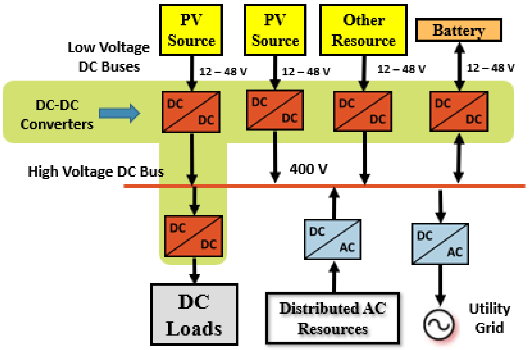
Figure 1. DC Microgrid System.
Energies 16 06950 g001
Figure 2. Modification of a conventional buck–boost DC–DC converter.
Energies 16 06950 g002
Figure 3. A modified buck–boost DC–DC converter [42].
Energies 16 06950 g003
Figure 4. Modified buck–boost converter with input LC filter (a) Li at the middle row of the topology, and (b) Li at the bottom of the converter.
Energies 16 06950 g004
Figure 5. Two-phase modified buck–boost converter.
Energies 16 06950 g005
Figure 6. (a) Cascaded configuration, and (b) a modular three-level modified buck–boost converter [33].
Energies 16 06950 g006
Figure 7. Two-phase input LC filtered modular multilevel DC–DC converter with controlled last cell.
Energies 16 06950 g007
Figure 8. Switching signal, current, and voltage waveforms for the converter in Figure 7. (a) Switching signal for switches SA1 and SA3. (b) Switching signal for switches SA2 and SA4. (c) Switching signal for switches SC1 and SC3. (d) Switching signal for switches SC2 and SC4. (e) Inductor current of the last cell. (f) Inductor current of the first cell (constant 0.5 duty cycle). (g) Total output voltage and input and output voltage of the last cell. (h) Total output voltage and input and output voltage of the first cell.
Energies 16 06950 g008
Figure 9. Comparison currents and voltages in CCM (ad) and DCM (eh). (a) Inductor current of last cell in CCM. (b) Inductor current of first cell in CCM. (c) Total output voltage and input and output voltage of the last cell in CCM. (d) Total output voltage and input and output voltage of the first cell in CCM. (e) Inductor current of last cell in DCM. (f) Inductor current of first cell in DCM. (g) Total output voltage and input and output voltage of the last cell in DCM. (h) Total output voltage and input and output voltage of the first cell in DCM.
Energies 16 06950 g009
Figure 10. RMS input ripple-current comparison between single-phase and two-phase modified buck–boost converters.
Energies 16 06950 g010
Figure 11. Voltage conversion ratio comparison between controlling the first cell (Mfirst) and the last cell (Mlast).
Energies 16 06950 g011
Figure 12. Experimental waveform. (a) Voltage across the switch (drain to source). (b) Current through switch (drain to source). (c) Current through L. (d) Voltage across C. (e) Output voltage (Vout = Ed + VC). (f) Output current (to load).
Energies 16 06950 g012
Figure 13. Efficiency of the basic cell of the proposed MMC for various voltage gain and load current.
Energies 16 06950 g013
Figure 14. Experiment setup for the 1-level modified buck–boost converter.
Energies 16 06950 g014
Figure 15. Experimental results of single-phase and two-phase input current modified buck–boost with input LC filter.
Energies 16 06950 g015
Figure 16. Ripple cancellation of inductor currents at half duty cycle in two-phase modified buck–boost converter.
Energies 16 06950 g016
Figure 17. Experiment setup for 3-level MMC version of the proposed modified buck–boost converter.
Energies 16 06950 g017
Figure 18. Experimental results of the voltage of each cell at 24 VDC input.
Energies 16 06950 g018
Figure 19. Calculation and experimental results for the first-cell-controlled and last-cell-controlled of the proposed converter.
Energies 16 06950 g019
Table 1. Simulation parameters.
ComponentsValueUnit
Inductors1mH
Capacitors30µF
Filter inductor46µH
Filter capacitor10µF
ESR of inductors0.3
MOSFET On-resistance0.04
Table 2. Comparison between the proposed topology and some of the previous topologies.
TopologyApplicationNo. of ComponentsBidirectionalVoltage GainCurrent
Ripple
[12]Auxiliary power supplies2N switches
2(N − 1) diodes
2(N − 1) capacitors
NoN(2N)
for even
N(2N + 1)
for odd
Moderate
[13]High-voltage-gain applicationN × M + (2N − 2) switches
N × M
capacitors
No(N − 1) M + 1
N = number of cap. in each stage
M = number of stages
High
[18]DC Link, hybrid PV systems2 switches
2 inductors
N capacitors
N diodes
No N 1 α Zero
[25]High step-up applications1 switch
5 diodes
4 inductors (3-coupled)
4 capacitors
No 1 1 α 2 .
2   n 2 + n 3 1 n 2 1
n2 = turns ratio inductor 2
n3 = turns ratio inductor 3
Moderate
[32]Grid-connected PV/fuel cell systems2 switches
6 diodes
2 coupled inductors
6 capacitors
No 4 + 2 N 1 α Zero
[44]DC microgrid2N switches
2N inductors
2N capacitors
Yes 1 + N   α 1 α Low
ProposedDC microgrid, distributed generation4N switches
2N inductors
2N capacitors
Yes M f i r s t = 1 + N 1 α 1 α

M l a s t = N N 1 α 1 α
Zero
Table 3. Experiment Parameters.
NoParameterValue
1MOSFET typeIRFP260N
2Li47.8 μH
3Ci10 μF, film capacitor
4L1 mH, ensures CCM
5C30 μF, film capacitor
6fs20 kHz
7Ed24 VDC
Disclaimer/Publisher’s Note: The statements, opinions and data contained in all publications are solely those of the individual author(s) and contributor(s) and not of MDPI and/or the editor(s). MDPI and/or the editor(s) disclaim responsibility for any injury to people or property resulting from any ideas, methods, instructions or products referred to in the content.