Article

A Study on the Distributed-Control Architecture of a DSP-Based Solid-State Transformer System with Implementation

School of Electronic and Electrical Engineering, Dankook University, Yong-In 16890, Republic of Korea
*
Author to whom correspondence should be addressed.
Energies 2023, 16(16), 6095; https://doi.org/10.3390/en16166095
Submission received: 3 July 2023 / Revised: 14 August 2023 / Accepted: 17 August 2023 / Published: 21 August 2023
(This article belongs to the Section F: Electrical Engineering)

Abstract

:
This article proposes a Distributed-control Architecture (D-CA) and an operation sequence with start-up strategies for a Digital Signal Processor (DSP)-based Solid-State Transformer (SST). Although various control techniques for SSTs have been reported in earlier studies, there is still a lack of research covering comprehensive content, including hierarchical control architectures and operation sequences with start-ups considering the implementation of DSPs. Therefore, this article addresses the following factors of SST. First, the D-CA is described for the design of the hierarchy between control boards. With the D-CA, because sub-boards are in charge of their corresponding DC-link voltage balancing control individually, the computational burden on the master board can be reduced. Second, the operation sequence of the SST system is explained based on the SST with D-CA. The step of DC-link voltage balance is considered throughout the entire operation sequence for safe driving. Furthermore, the PWM start-up strategies for a Cascade H-bridge Multilevel (CHM) converter and Dual Active Bridge (DAB) converter are proposed to prevent switching pulse errors caused by DSP operating characteristics. These start-up strategies reduce the current surges. The validity of the proposed D-CA and operation sequence with start-up strategies are verified by experimental results.

Graphical Abstract

1. Introduction

Recently, driven by environmental concerns and carbon dioxide regulations, industries are undergoing extensive electrification. The progress in high-capacity energy storage devices, such as batteries and supercapacitors, along with advancements in complementary technologies like sensing and lifespan prediction, is accelerating this trend [1,2].
Furthermore, powered by advancements in power semiconductor technology, traditional passive power conversion systems are being replaced by power semiconductor-based converters. Notably, among these advancements, the Solid-State Transformer (SST) stands out as a leading next-generation technology, positioned to replace conventional oil-immersed transformers. The SST has advantages, including voltage sag compensation, bidirectional power flow, and improved power quality [3,4,5,6,7,8]. Additionally, the system size and weight can be reduced compared to conventional transformers. Thanks to these advantages, the SST has found applications in diverse fields such as smart grids, transportation, and renewable energy sources [9,10].
Various SST topologies have been investigated in many studies [11]. Among the SST topologies, the system for generating DC output is applied to applications such as railways and microgrids. Moreover, the SST consisting of a Cascaded H-bridge Multilevel (CHM) converter and Dual Active Bridge (DAB) converters for the AC-DC and DC-DC conversions, respectively, is used widely. This structure can control various output voltage levels and support bidirectional power transmission with galvanic isolation [12,13,14].
To configure an SST with CHM and DAB converters, proper control techniques are necessary at each power conversion stage. In a CHM converter, DC-link voltage control and grid-connected current control are performed, whereas a DAB converter is in charge of voltage control for DC output. Those control techniques for CHM and DAB converters were introduced in [15,16,17], individually.
In addition to the control techniques described above, assistive techniques were also reported, namely, DC-link balancing control, dead time compensation, and harmonic reduction. As voltage imbalances between DC-links of cells increase stress to the IGBTs and DC-link capacitors in a CHM converter, balancing control should be applied. DC-link balancing control can be conducted by either a CHM converter or a DAB converter. In [18], the CHM converter carries out DC-link balancing by individually adjusting the switching reference voltages of H-bridges. In contrast, in earlier work [19], another method using a DAB converter was introduced.
Modulation methods for CHM and DAB converters were also studied. The modulation methods for the CHM converter are classified into Level-Shifted Pulse-Width Modulation (LS-PWM) [20,21] and Phase-Shifted Pulse-Width Modulation (PS-PWM) [21,22,23]. In PS-PWM, the output voltage level for each cell is constant. In addition, losses are equally distributed for all cells, avoiding biased large losses to particular switches. DAB converter modulations were reported in [24,25]. Ref. [24] described the conventional PS-PWM controlled by the phase difference between the primary and secondary voltages, and [25] presented a hybrid modulation through the feedback-linearized controller.
The above studies dealt with the control techniques of CHM and DAB converters individually, which means that a discussion of the system operation of the SST was needed. Accordingly, a description of the overall system operation was reported in [26,27,28,29,30,31]. A comparative summary of the overall reference is available in Table 1. Refs. [26,27] presented the overall control sequence. However, the control architectures and operation sequences, which are important for the actual implementation, were not presented in detail. In particular, Ref. [26] only discussed the initial charging technique of the capacitors to protect against short-circuit accidents at the start of control. To mitigate switching pulse errors, a start-up strategy is additionally required to mitigate switching pulse errors.
Unlike [26,27], Ref. [28] presents a control hierarchical architecture. While Ref. [28] presents an appropriate architecture based on various SST topologies, it does not include control sequences and communication structure. Similarly, Ref. [29] shows a control hierarchical architecture. The control process of [27] is presented in detail compared to [28]. However, Ref. [29] also required an explanation of the communication structure and the control sequence. Refs. [30,31] proposed the entire operation sequence and the control hierarchical architecture. Especially, Ref. [31] indicated the output waveforms of the control sequence, but the DC-link voltage balancing control was omitted. Furthermore, data transmission relations between control boards within the suggested control architecture were not specified in [30,31]. In other words, the controls of SST, including communication transmission between cells, are not fully organized.
As described above, although various studies on the SST have existed, there is a lack of articles covering comprehensive content, including hierarchical control architectures and operation sequences with start-up strategies considering the implementation of DSPs. Therefore, we address the following factors of SST systems based on a laboratory prototype. First, a hierarchical control architecture, the Distributed-control Architecture (D-CA), for the design of a DSP-based SST system is proposed. Unlike earlier studies where a master board is fully in charge of the entire control and sub-boards on cells exist just for PWM switching, in the D-CA, sub-boards have a dedicated DC-link voltage balancing controller individually for their corresponding cells. With this strategy, the computational burden on a master board can be reduced. Considering DSP environments, detailed figures with data transfer of communication between a master board and sub-boards are illustrated. Second, based on the designed SST with D-CA, the entire operation sequence of the SST system is described. A step of DC-link voltage balance is considered throughout the entire operation sequence for safe driving. Furthermore, the start-up strategy of CHM and DAB converters is explained, especially focusing on the aspect of the DSP. The strategies deal with the switching pulse errors associated with DSP characteristics in order to prevent a current surge.
The rest of this article is organized as follows. Section 2 explains the system configuration and control techniques of the SST. Section 3 suggests the D-CA with descriptions of DSP operation in the time domain. In Section 4, the entire operation sequence of the SST is described with start-up strategies for the CHM and DAB converters. Section 5 presents the experimental results to prove the validity of this proposal. Finally, Section 6 concludes this article.

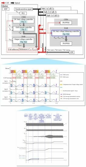
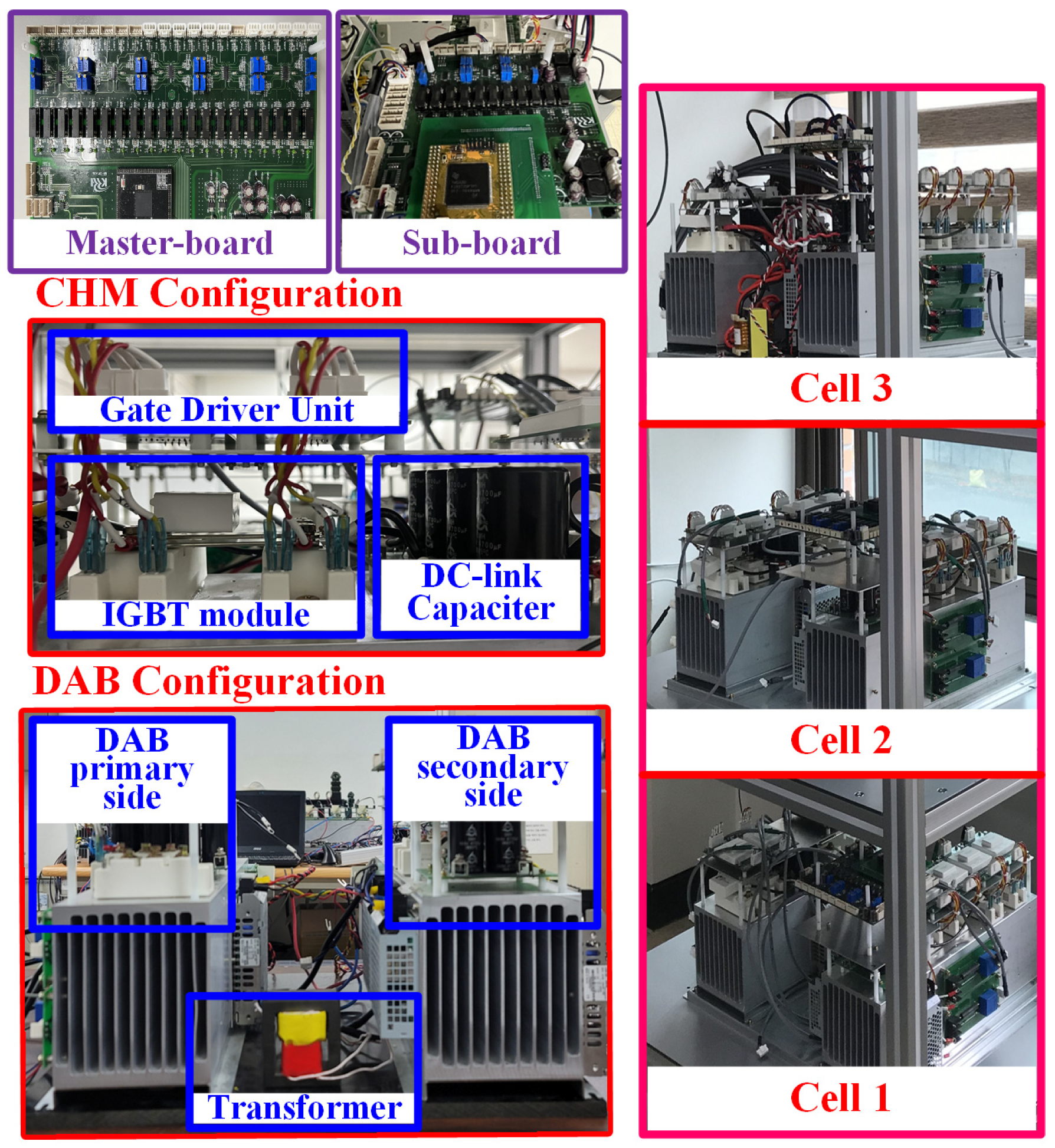
2. SST System Configuration

In this article, all descriptions are based on the designed single-phase SST shown in Figure 1. This section explains the overall system configuration seen in the figure. The SST system consists of the 3-cell CHM converter in Figure 1a and DAB converters in Figure 1b. The CHM converter is connected to a single-phase grid ( v g ), through an AC filter inductor ( L ). Each H-bridge of the CHM converter is connected to each DAB converter, and the DAB converters are in parallel for the generation of output voltage ( v o u t ). This structure is called Input Series Output Parallel (ISOP). In front of the CHM converter, there is a pre-charge circuit to prevent inrush currents in DC-link capacitors.
In Figure 1a, the CHM converter stacks the output voltages of each cell by connecting H-bridge converters in series. The maximum available level (m) of an output voltage of the CHM converter ( v C H M ) is calculated as
m = 2 H + 1  
where H is the number of H-bridge converters connected in series. As this article is described based on a three-cell topology, output voltages can be generated for up to seven levels. The output voltage level is fixed by a Modulation Index (MI), and if the MI is bigger than 0.67, a seven-level voltage is formed. The MI formula is given as
MI = V g × 2 V d c l i n k t o t a l  
In (2), V d c l i n k t o t a l means the sum of the DC-link voltage of the cells.
The DAB converter is an isolated DC-DC converter, which steps down DC-link voltage to output voltage. The DAB converter can transfer power bi-directionally and has the advantages of providing relatively low voltage stress and a low passive component rating [32]. In Figure 1b, the DAB converter is composed of H-bridge converters with a medium frequency transformer (MFTR). Input capacitors correspond to DC-link capacitors, and output capacitors are in a parallel configuration.

3. Design of D-CA for SST

This section describes the control architecture designed for the operation of the SST system in Figure 1 with a DSP. For practical fulfillment, control techniques of voltages and currents and the communication protocol with data transfer are illustrated.

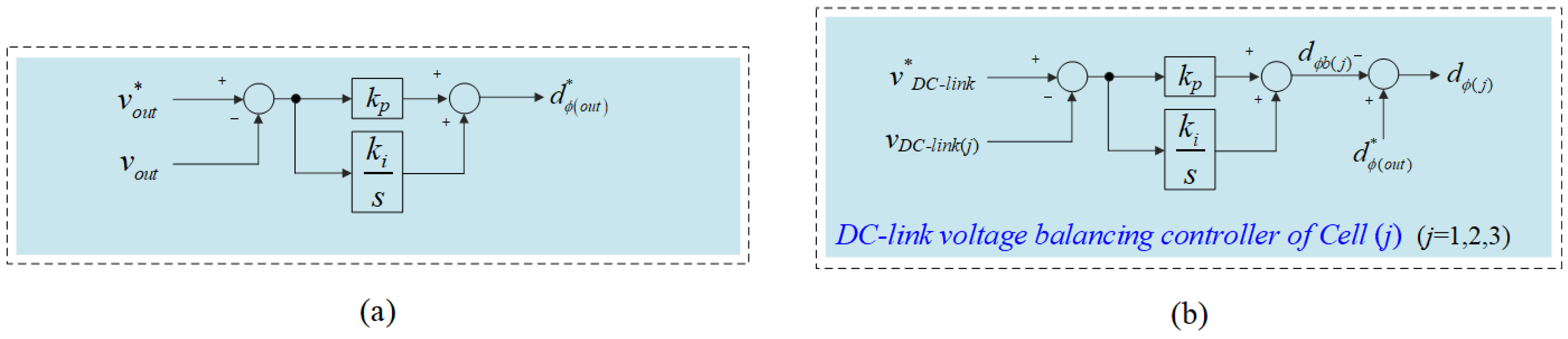
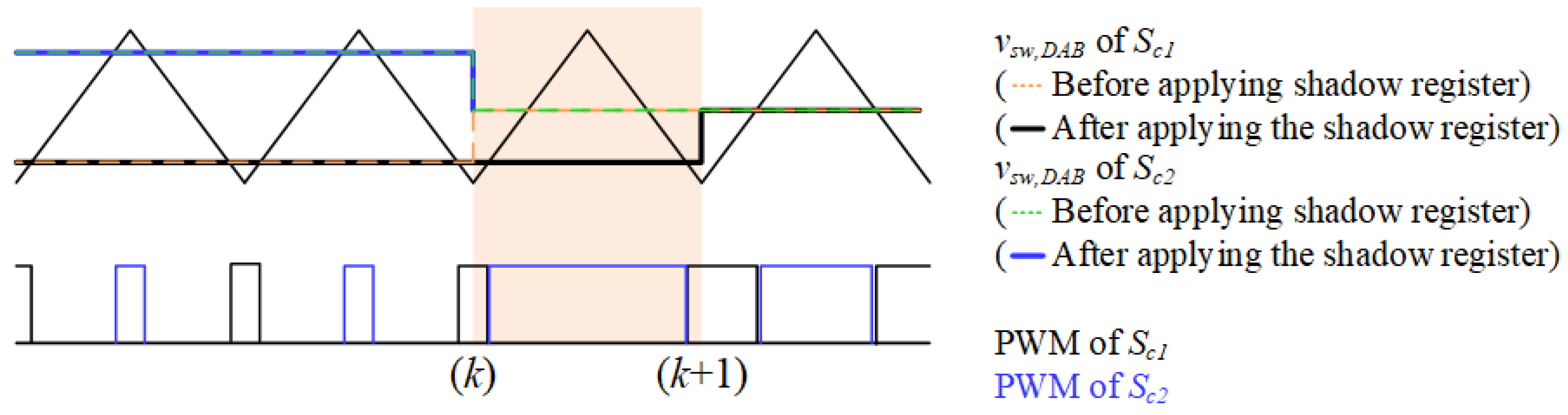
3.1. Control Technique of CHM and DAB Converters

In this subsection, before describing the hierarchical control architecture of the SST, we describe the individual techniques for voltage and current controls. The control techniques are classified according to power conversion stages (i.e., CHM or DAB converter). Figure 2 and Figure 3 depict controllers of the CHM and DAB converters, respectively.
Figure 2 is composed of a DC-link voltage controller and a grid current controller, which are the outer and inner controllers, respectively. The DC-link voltage controller operates prior to the grid current controller in order to generate the active grid current reference ( i q e ) that is responsible for charging and discharging of DC-link capacitors. This process is realized by eliminating the error between the DC-link voltage reference ( v d c l i n k t o t a l ) and v d c l i n k t o t a l using a Proportional-Integral (PI) controller. After the DC-link voltage control, the grid current control is conducted by PI controllers to control dq-axis currents in the synchronous reference frame ( i d q e ), resulting in v d q e b f . Throughout the current control, it should be noted that the d-axis current ( i d e ) remains at zero for the unity power factor control. Subsequently, the feedforward component for grid voltage ( v f f ) is added to v q e b f . The phase angle ( θ e ) of the grid voltage given by the Phase-Locked Loop (PLL) using an All-Pass Filter (APF) is used to transform v d q e b f to v d q s b f in a reverse manner. After that, dead time compensation ( v d t ) is added; a switching reference voltage of CHM converter ( v f i n ) for PS-PWM is derived. The phase shift angle ( ϕ c r ) for the PS-PWM is calculated as
ϕ c r = 180 m 1 ° .  
Therefore, based on (1) and (3), ϕ c r between carriers of each cell is given as 60° in this article.
Regarding the DAB converter, the phase shift angles for PS-PWM ( d ϕ j ) are derived. The power transfer equation of the DAB converter in relation to d ϕ j is expressed as
P = n v d c l i n k j v o u t 2 L f s d ϕ j 1 d ϕ j ,  
where n and f s represent a winding ratio and switching frequency, respectively. To obtain d ϕ j , controls are conducted by being distinguished as an output voltage controller and DC-link balancing controllers as shown in Figure 3a,b, respectively. The output voltage controller consists of a PI controller for eliminating the error between v o u t and its reference value ( v o u t ), with the result that d ϕ o u t is generated. The DC-link balancing controller’s control v d c l i n k 1 to v d c l i n k 3 to track their nominal value v d c l i n k , forming d ϕ b j . Subsequently, d ϕ j is calculated by subtracting d ϕ b j from d ϕ o u t .

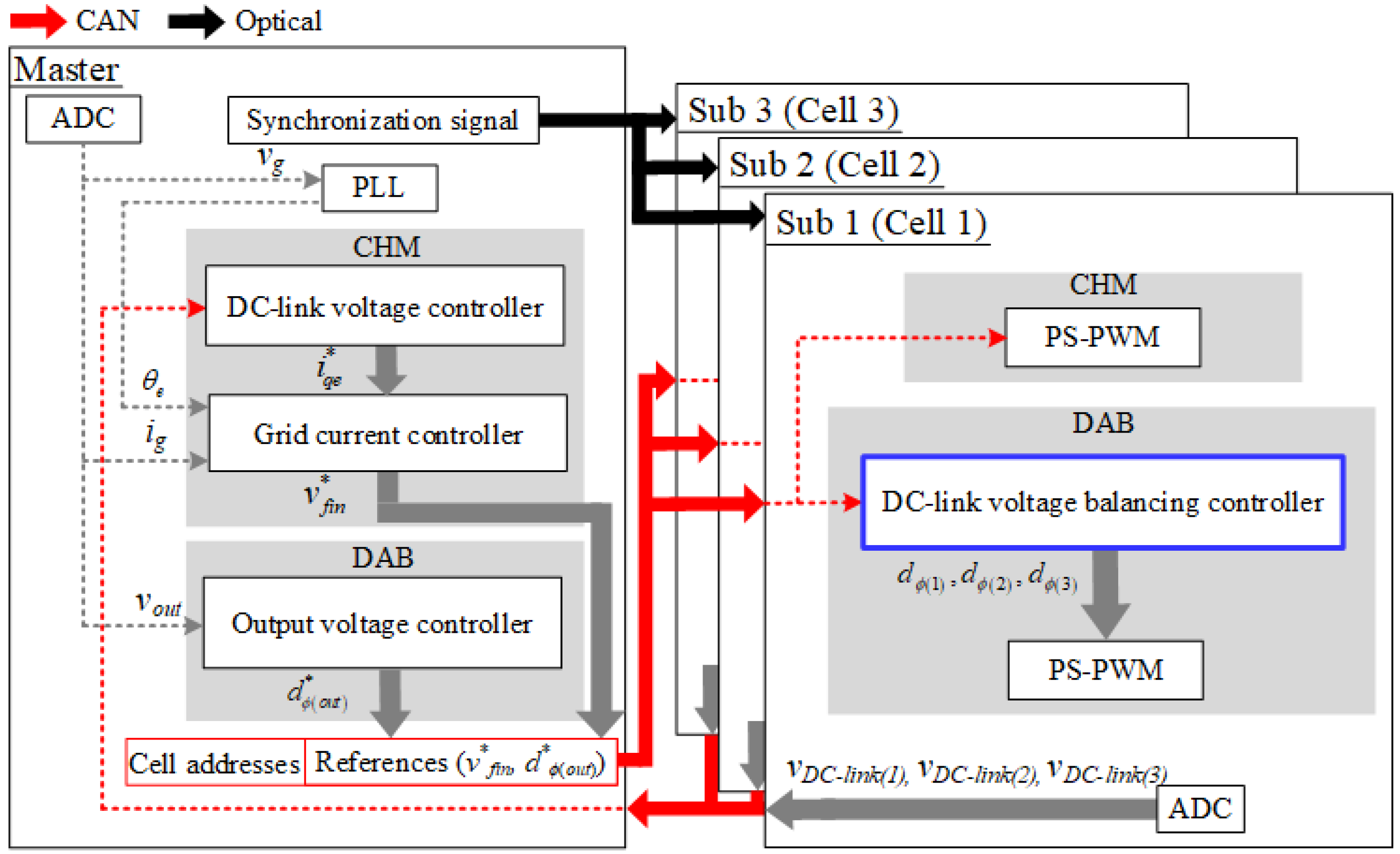
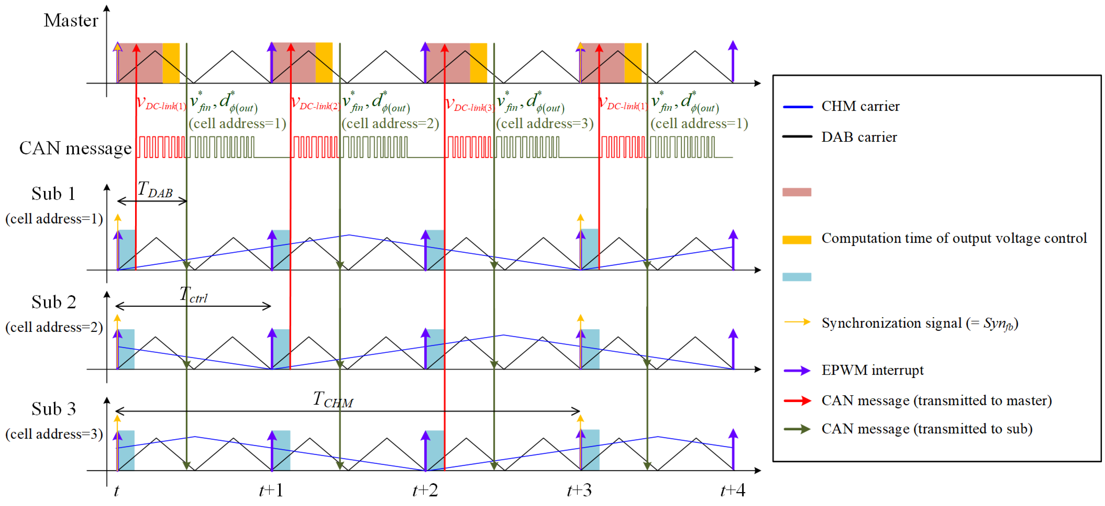
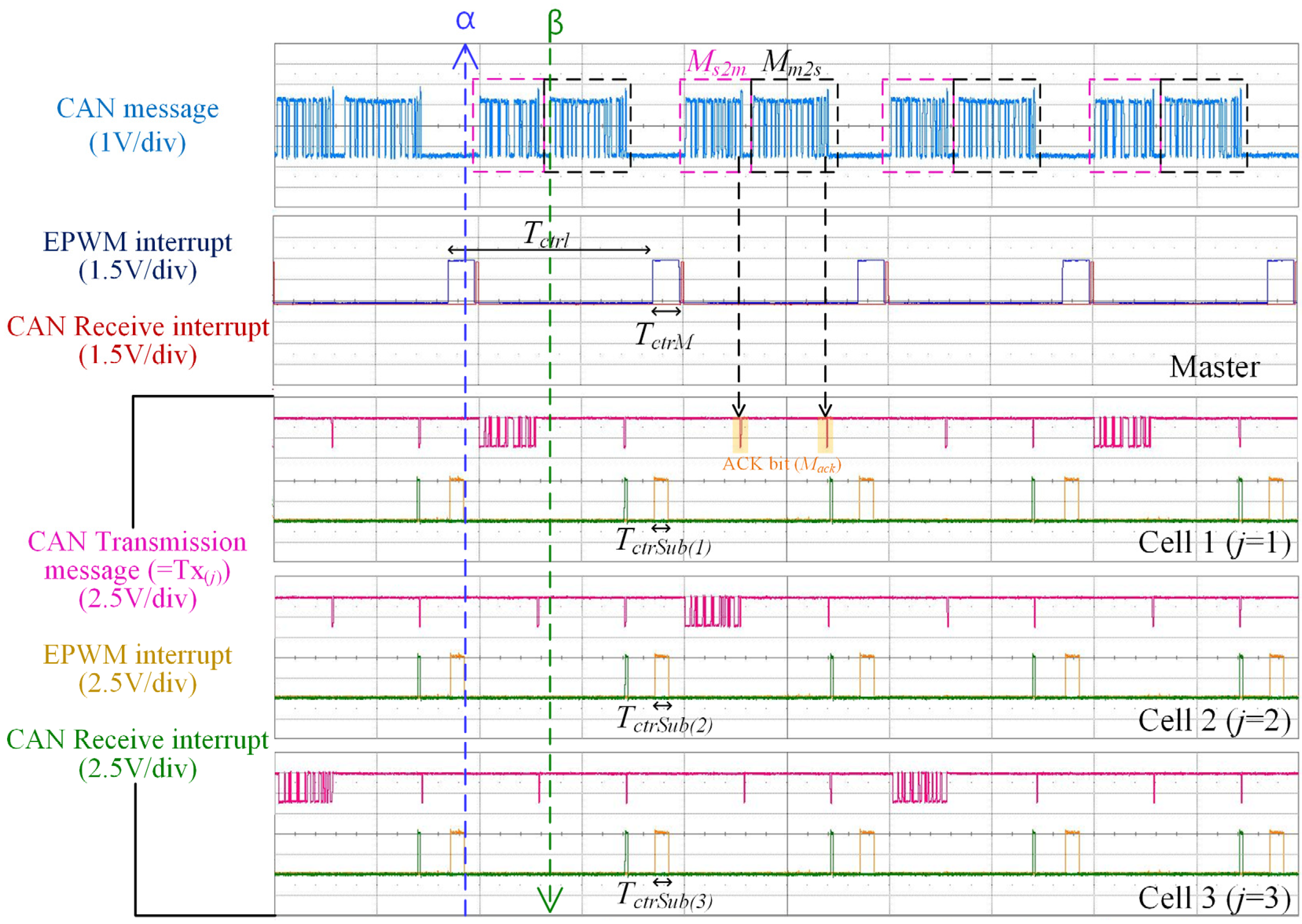
3.2. Distributed-Control Architecture (D-CA)

Figure 4 shows the design of the hierarchical control architecture for implementing the control techniques to the SST system configuration of Figure 1. The proposed control architecture physically has four control boards, classified into three sub-boards distributed to respective cells (Sub 1 to Sub 3) and one master board. Between the control boards, a communication line through the Controller Area Network (CAN) for data transfer and an optical fiber for synchronization is also depicted.
The master board carries out overall system controls for the generation of v o u t , such as PLL, DC-link voltage control, grid current control, and output voltage control of the DAB converter. For these controls, actual values for v g , i g , and v o u t are directly obtained through the Analog-to-Digital Converter (ADC), whereas v d c l i n k 1 to v d c l i n k 3 is received from sub-boards through the CAN. Upon finishing the entire control, the master board transmits reference values v f i n and d ϕ o u t with a cell address to the sub-boards. Here, the cell address is assigned integer values according to the cell number, which is explained later in the next figure.
The sub-boards are mainly in charge of the PS-PWM for its corresponding cell, as depicted in Figure 4. However, it should be noted that the DC-link voltage balancing control is also conducted. This structure is denoted as a hierarchical control architecture with distributed control (D-CA) in this article. General control architectures where controllers are all arranged in a master board suffer from a high computational burden because the number of DC-link voltage balancing controllers increases with the increment of cells. In contrast, the D-CA can achieve a low computational burden on the master board regardless of the number of cells due to the distribution of those controllers. Due to this mechanism, v d c l i n k 1 to v d c l i n k 3 is acquired in their corresponding sub-boards.
Figure 5 shows the operation of the D-CA with respect to the aspect of the DSP in the time domain. In the figure, the control computation times, EPWM interrupt, synchronization signal ( S y n f b ), CAN message, and triangular carriers of the CHM and DAB converters are indicated. The EPWM interrupts of the sub-boards are synchronized by S y n f b generated every three cycles of the EPWM interrupt of the master board. As all controls operate every EPWM interrupt, a control period ( T c t r l ) is identical to the interval between the present and the next EPWM interrupt. In this article, the carrier periods of the CHM and DAB ( T C H M , T D A B ) converters are set to three times and a half of the control period, respectively.
As shown in Figure 5, data transfer through the CAN between control boards starts after the controls end. One can note that data from the master board (i.e., the cell address, v f i n , and d ϕ o u t ) are transmitted every T c t r l , whereas data from the sub-boards (i.e., v D C l i n k j ) are sent every three cycles of T c t r l alternately. The sub-boards receive a cell address, which changes from one to three every control period; thus, only one cell with the same address requested by the master board sends v D C l i n k j to the master board. For instance, Sub 2 transmits v D C l i n k 2 at t + 2 because the cell address at t + 1 is two. This is due to the consideration of communication speed when one CAN bus is used. As the DC-link voltage controller does not require a relatively high dynamic response, this strategy is reasonable.

4. Operation Sequence with Start-Up Strategies

In this section, first, we explain the entire operation sequence for the designed SST based on D-CA for seamless and safe driving. Second, we describe the specific strategy of the start-up operation considering DSP implementation in order to prevent current surges from deteriorating the stability of the SST system. The start-up strategy described aims to eliminate switching pulse errors that are generated at the PWM operation immediately after the start of control.

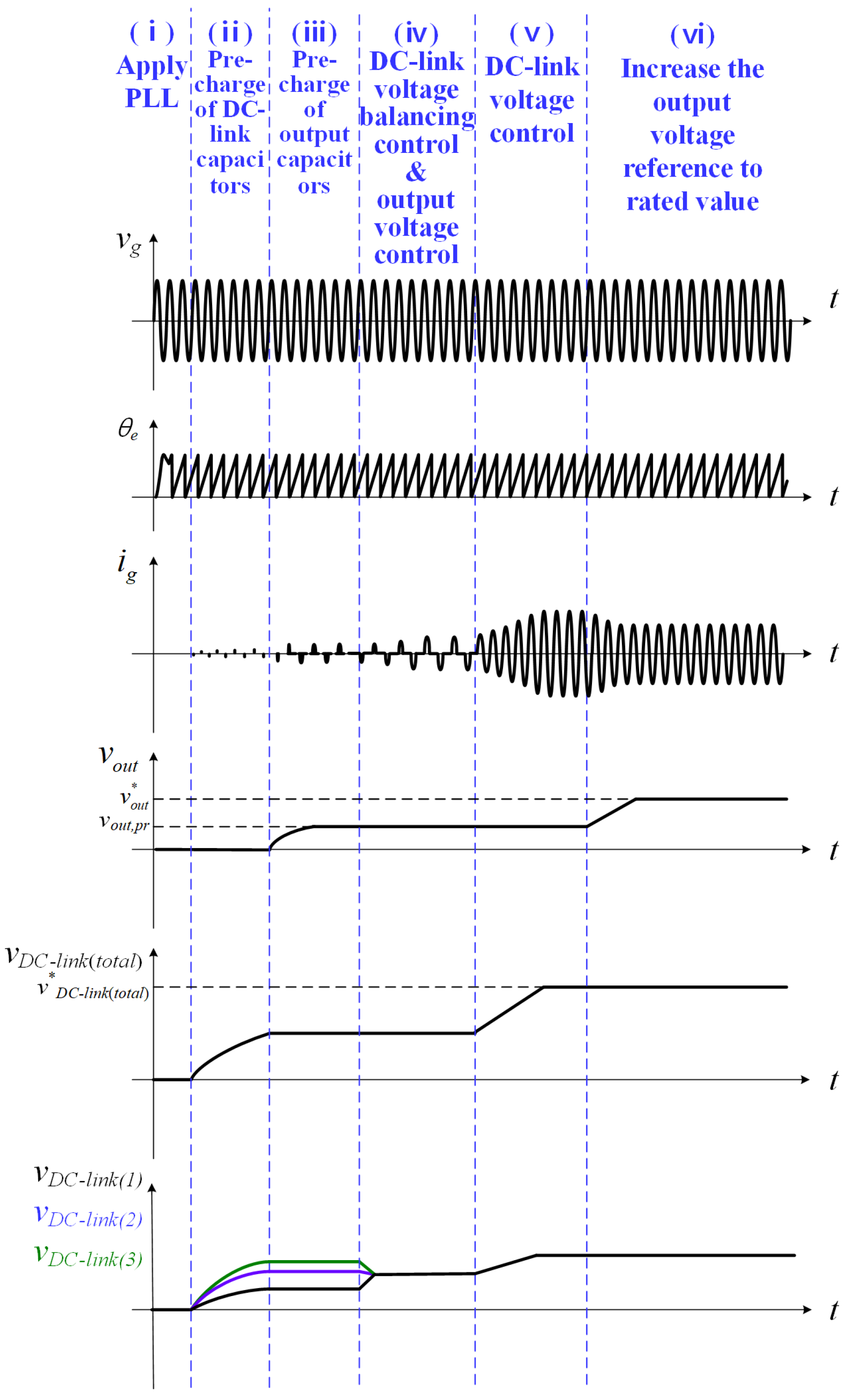
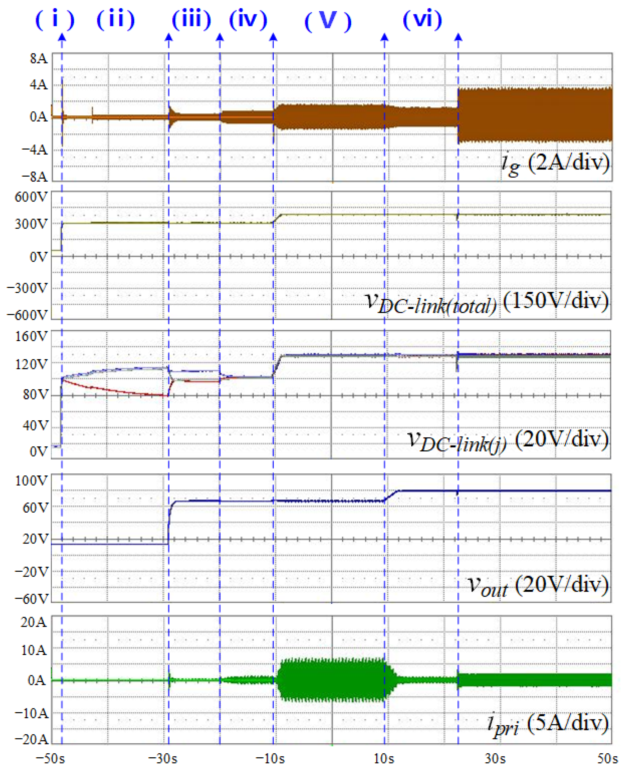
4.1. Operation Sequence

The entire operation sequence of SST is explained based on Figure 6, which shows sequential output waveforms. Operation points are distinguished by the number denoted in Figure 6 (i.e., (i) to (vi)).
In (i), the PLL is operated to estimate θ e . Next, the pre-charge of the DC-link and output capacitors are sequentially executed in (ii) and (iii), respectively, in order to prevent capacitor failure. For the DC-link capacitors, the pre-charge circuit is given as shown in Figure 1. Switch S 1 is turned on to attach the pre-charge resistor R until the DC-link voltage reaches a steady state. After that, S 2 is turned on to connect the CHM converter to the grid, but S 1 is detached. It can be seen that v D C l i n k j and v D C l i n k t o t a l are slowly charged in (ii) in Figure 6.
Regarding output capacitors, the pre-charge is conducted by the PWM technique without an extra pre-charge circuit. In this case, PWM with a small duty cycle is imposed on the primary side of the DAB converter; however, the PWM of the secondary side remains in an off-state; thus, v o u t is charged slowly up to the pre-charged values ( v o u t , p r ) determined by a turn ratio of the MFTR, as depicted in (iii) in Figure 6. A detailed explanation is given in Section 4.3.
Once the pre-charge operations in (ii) and (iii) are completed, the balancing control and output voltage control are executed in (iv). It should be noted that v D C l i n k j is in an unbalanced condition as shown in (ii) and (iii) due to the possibility of slight capacitance differences. This implies that DC-link voltage balancing controls should be implemented prior to the DC-link voltage control of the CHM converter in order to prevent damage to the DC-link capacitors and power semiconductors. Therefore, in (iv), it can be seen that v D C l i n k j becomes balanced. Regarding v o u t , it is controlled to v o u t , p r .
Subsequently, in (v), the DC-link voltage control of the CHM converter is performed and v D C l i n k t o t a l increases to the rated value via a ramped increase. Here, as the DC-link voltage balancing is already in operation, v D C l i n k j values remain the same as each other even in a transient state. Finally, in (vi), v o u t increases to generate a rated DC output voltage.

4.2. Start-Up Strategy of CHM Converter

Figure 7 shows a PS-PWM of the CHM converter when (v) starts. In the figure, the start-up signal determines the start of the switching pulse output, and the point where the start-up signal becomes one is called the start-up point. At the start-up point, v f i n is calculated by grid current control. v f i n is compared to the CHM converter carriers ( C a r r C H M s ) of each cell to the output PWM. The PWMs of S a 1 , S a 3 , and S a 5 , which are the upper left switches for each cell, are representatively depicted.
The PWM is implemented when v f i n and C a r r C H M meet. According to the setting of the DSP, if the slope of C a r r C H M is positive and equal to v f i n , a high state is derived (PWM = 1). In contrast, if the slope is negative, the PWM is converted to a low state (PWM = 0). Figure 7a,b confirm that the PWMs are output depending on the previously mentioned DSP settings.
Since the default of the PWM ( S W d e f a u l t ) is set to low, several PWMs, which should begin at a high state, cause an error. For example, all cells must begin PWM at a high state because v f i n has a value greater than 0.66 in Figure 7a. However, since S W d f a u l t is at a low state, PWM remains at a low state until v f i n and the negative slope of C a r r C H M become equal. Therefore, the PWM of Sa1, S a 3 , and S a 5 does not initiate at a high state. This PWM error is referred to as a pulse omission. The pulse omission leads to an error in the DC-link voltage control and results in a surge of i g .
To address the pulse omission in some PWMs, in this article, a start-up strategy with a S W d e f a u l t setting is given. The start-up strategy compares the magnitude of v f i n with the size of C a r r C H M at the start-up point. If v f i n is larger than C a r r C H M , S W d e f a u l t is set to a high state to create a pulse at the start-up point. Based on the 3-cell SST, the S W d e f a u l t setting is given as
Cell   1 :   S W d e f a u l t = high
Cell   2 : { S W d e a u l t = low   ( v f i n < 0.33 )   S W d e a u l t = high   ( v f i n > 0.33 )
Cell   3 : { S W d e a u l t = low   v f i n < 0.66   S W d e a u l t = high   v f i n > 0.66 .
With (5), the pulse omission can be solved as shown in Figure 7b. It can be seen that switching pulses appear without omission, with the result that a surge of i g decreases compared to that of Figure 7a.

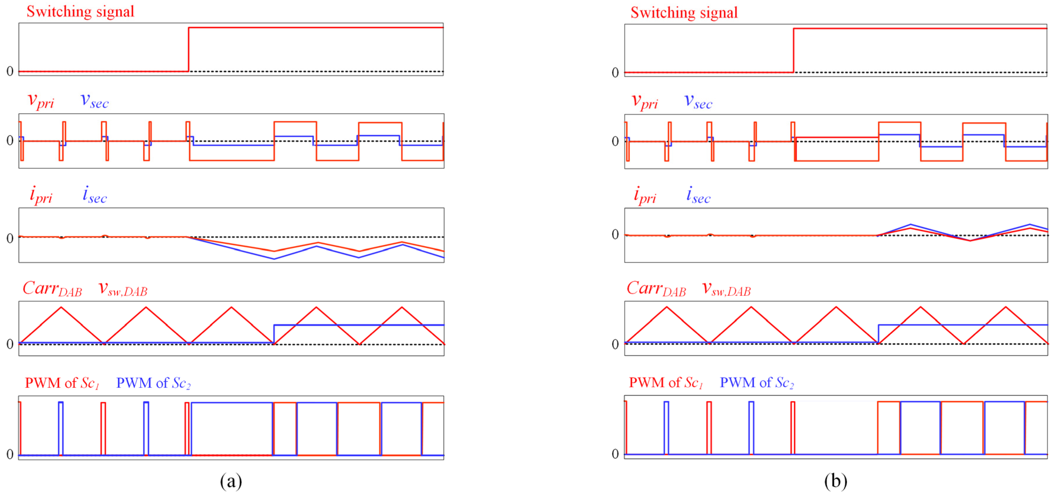
4.3. Start-Up Strategy of DAB Converter

Figure 8 shows the waveforms of the DAB converter start-up. At the transition point where the switching signal becomes one, the operation sequence changes from (iii) to (iv), shown in Figure 6. In Figure 8, v p r i and v s e c refer to the primary and secondary voltages of the MFTR, respectively. i p r i and i s e c indicate the primary and secondary currents of the MFTR, respectively. The DAB carrier is C a r r D A B , and v s w , D A B means a switching reference of the DAB converter. In this article, a small duty cycle for the pre-charge of output capacitors is set to 0.05, as depicted in the PWM waveforms at the bottom of Figure 8.
In Figure 8a, v s w , D A B is 0.5 after T D A B from the transition point. This delay is caused by a shadow register of DSPs, and Figure 9 depicts this phenomenon in detail. In the shadow register, the v s w , D A B is applied to the PWM by reflecting the past v s w , D A B at each zero of C a r r D A B . Consequentially, when the point (k) is the transition point, it can be seen that 0.5 v s w , D A B comes out from the point (k + 1). While it is possible to prevent the omission of pulses by v s w , D A B or C a r r D A B , which change at any point, it causes the wrong PWM from (k) to (k + 1).
If the wrong PWM is applied to the DAB converter because the PWM exceeds 0.5, the i p r i and i s e c lean to one polarity and increase as if with a DC offset. Therefore, all PWMs should be set to a low state for one cycle of T D A B after the transition point to eliminate the wrong PWM, as illustrated in Figure 8b. This low setting of PWM is referred to as a start-up strategy of the DAB converter. It can be confirmed that 0.5 duty is output after the transition point. As a result, i p r i and i s e c can be zero on average without a DC offset.

5. Experimental Results

We conducted an experiment to prove the validity of the designed SST with D-CA and the proposed operation sequence considering the DSP implementation. The experimental setup shown in Figure 10 has the same system configuration as Figure 1 and the parameters applied are denoted in Table 2. The master board and sub-boards consisted of DSPs named TMS320F28377D.

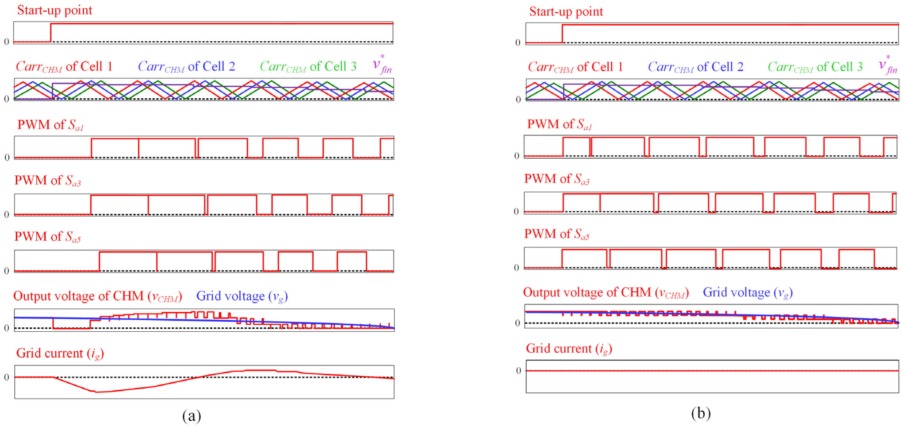
5.1. The Verification of D-CA

As illustrated in Figure 4, the D-CA with one CAN bus at 1Mbps speed was constructed in the experimental setup. Figure 11 shows the waveforms of the D-CA operation corresponding to Figure 5. The pulses in high states are the computation time of controls ( T c t r M , T c t r S u b j , j = 1, 2, 3) when EPWM interrupts occur, and hence the rising edge of those pulses indicates the points where EPWM interrupts are generated. It can be seen that all EPWM interrupts of the control boards are synchronized.
In the figure, the operation during a T c t r l can be explained as follows. First, in the master board, as soon as an EPWM interrupt occurs, the computation of the CHM converter control (i.e., PLL, DC-link voltage control of the CHM converter, and grid current control) and the DAB converter output voltage control are conducted, as shown in T c t r M . In the meantime, in the sub-boards, the computation of the DC-link voltage balancing control is performed, as depicted in TctrSub(j). Subsequently, the CAN message M s 2 m , containing data of v D C l i n k j , is transferred from one of the sub-boards to the master board at α. Finally, the CAN message M m 2 s , including data of v f i n , d ϕ o u t , is sent from the master board to all the sub-boards at β.
The pulse widths of the EPWM interrupts were the same as the computation time, as the control operation was performed by turning the EPWM interrupt on at the start of the control computation and turning it off at the end of the control computation. The division of the time axis in Figure 11 was 100 μs, where the computational time of the master board was approximately 150 μs, and the computation time of each sub-board was approximately 50 μs. In other words, it can be seen that the sub-boards covered 50 μs, which was a part of the computational burden that the master board did. As a result, it should be noted that T c t r S u b j is the computation time for the DC-link voltage balancing control and is taken in every sub-board simultaneously. In addition, in the T X j waveform, the 1-bit pulse except for M s 2 m is an ACK bit ( M a c k ) that indicates whether the message is an error or not. Mack was not sent to the master board.

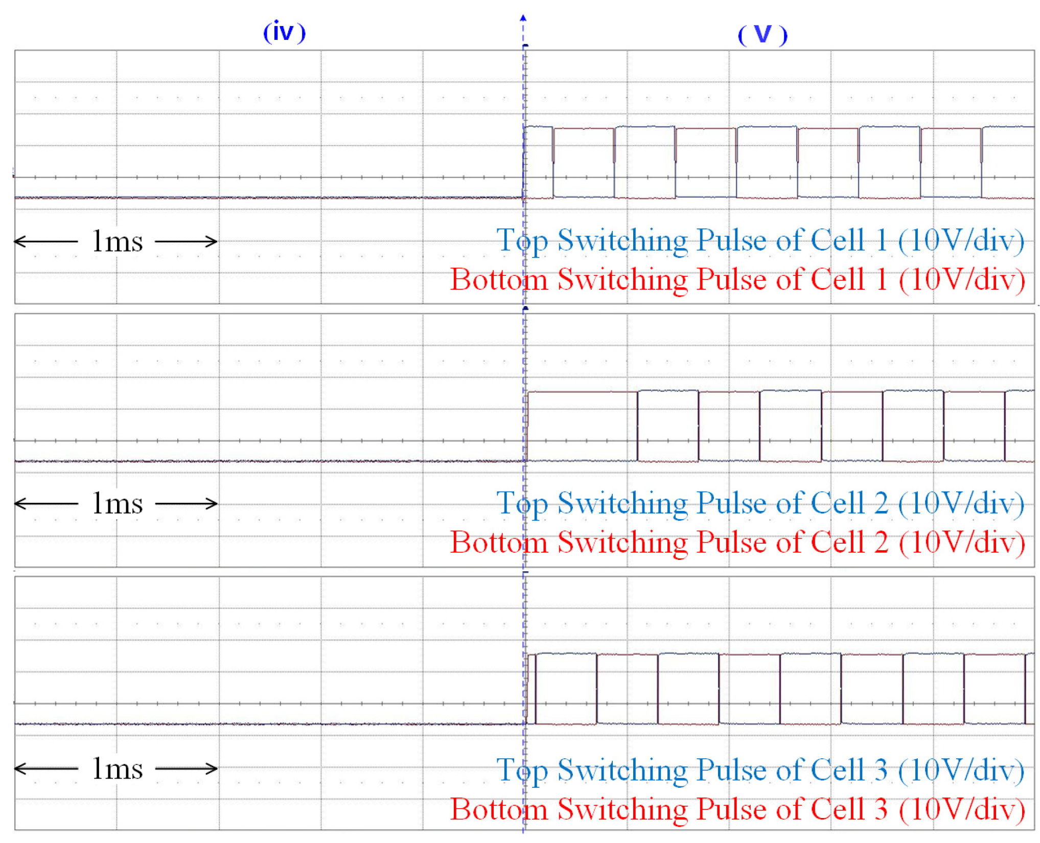
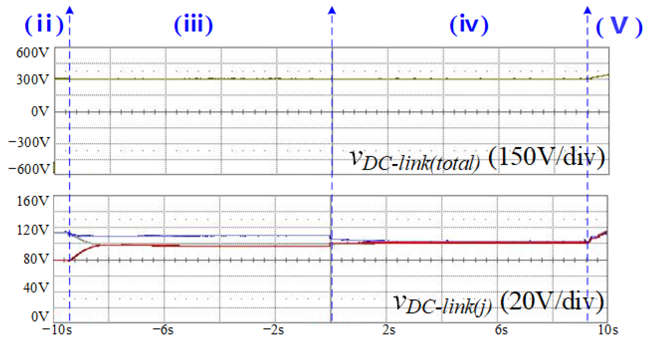
5.2. The Verification of Operation Sequence and Start-Up Strategy

The experimental result of the entire operation sequence according to Figure 6 is shown in Figure 12. It can be seen that the result is as same as in Figure 6. The pre-charge of DC-link capacitors is conducted in (ii) after PLL is completed in (i); thus, v D C l i n k t o t a l becomes approximately 311 Vpk, which is the magnitude of the input grid voltage. One can notice that v D C l i n k j is unbalanced in this region. Next, in (iii), the output capacitors are charged to v o u t , p r , which means v o u t becomes around 69 V due to the turn ratio of the MFTR. When the output capacitors are fully charged, the DC-link voltage balancing control and output voltage control are conducted in (iv). Subsequently, the DC-link voltage control of the CHM converter starts in (v), and v D C l i n k t o t a l increases up to the rated value of 390 V via a ramped increase. Once v D C l i n k t o t a l reaches a steady state, v o u t increases to the rated value 80 V in (vi). When v o u t is held in a steady state, the SST is fully ready; finally, a load is connected at the output of the SST. In this experiment, a step-load is applied, and hence i g and i p r i become larger immediately compared to that of (vi). It can be seen that v D C l i n k j and v o u t are controlled reliably despite a step load variation.
Figure 13 shows the zoomed extractions of v D C l i n k t o t a l and v D C l i n k j from Figure 12. v D C l i n k j has different voltage levels in (ii) and (iii), while v D C l i n k t o t a l is held constant. In contrast, they become balanced in (iv) due to the DC-link voltage control. As described in Section 4, the reason for the operation of (iv) prior to (v) is to prevent the situation where one of the v D C l i n k j exceeds the rating of components during the ascent of v D C l i n k t o t a l in (v).
Figure 14 shows the experimental results when the load changes to 12.5%, 25%, and 50% of the rated load. Although the output power changes in steps, v D C l i n k j and v o u t immediately track the reference values (i.e., 130 V and 80 V), indicating that the dynamic response of the designed controllers is fast enough. Furthermore, from Figure 14a–c, displaying the zoomed extraction at respective load conditions, it can be observed that both voltages remain stable, and i g exhibits sinusoidal waveforms.
Figure 15 shows a switching pulse at the start-up operation of the CHM converter when the sequence (v) starts. Due to the application of the CHM converter start-up strategy as in B in Section 4, switching pulses are output without omissions in all cells. Therefore, it is clear that there is no high surge of i g when (v) starts in Figure 12.
Figure 16 presents the switching pulses at the start-up operation of the DAB converter when the sequence is transferred from (iii) to (iv). In (iii), the switching pulses with a small duty cycle (0.05) are applied for the slow pre-charge of the output capacitors. Subsequently, in the transfer region from (iii) to (iv), it can be seen that the switching pulses follow those of Figure 8b due to the DAB converter start-up strategy as in Section 4.3. Therefore, at the start of (iv) in Figure 12, the magnitude of i p r i is not negatively biased.

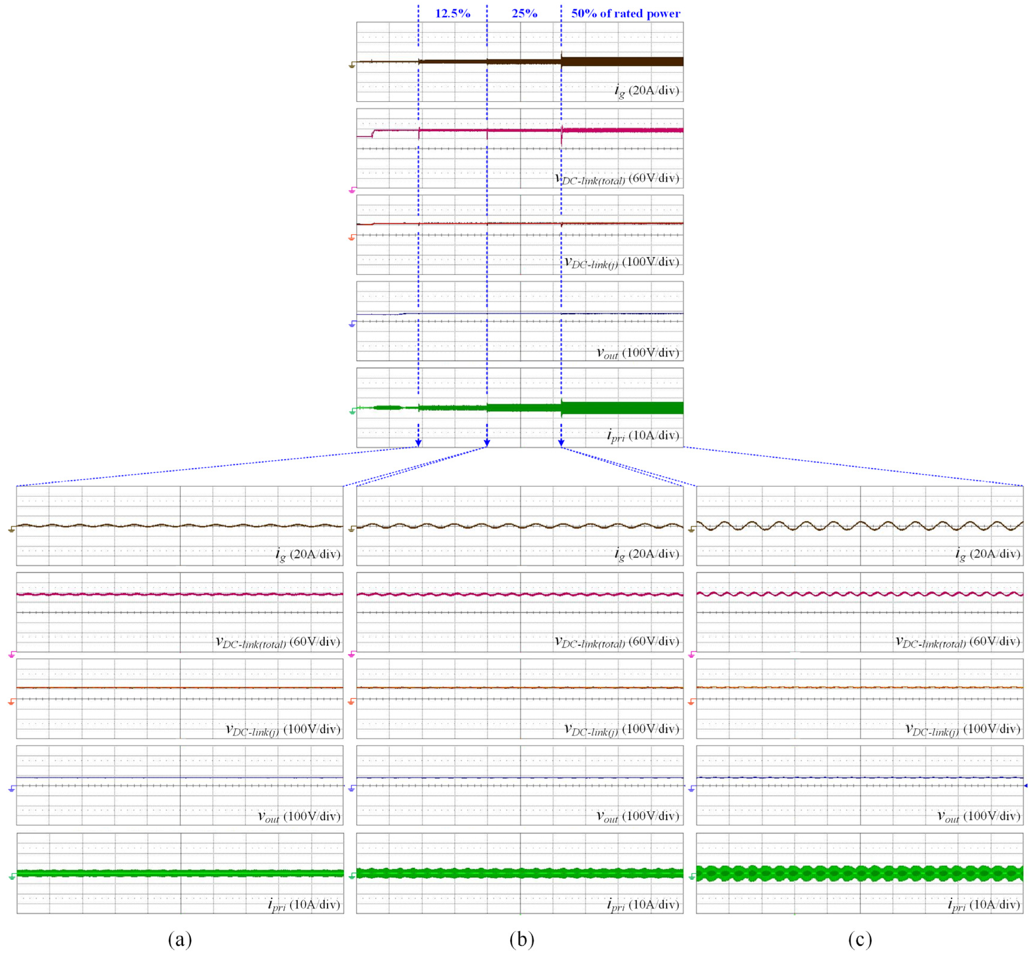
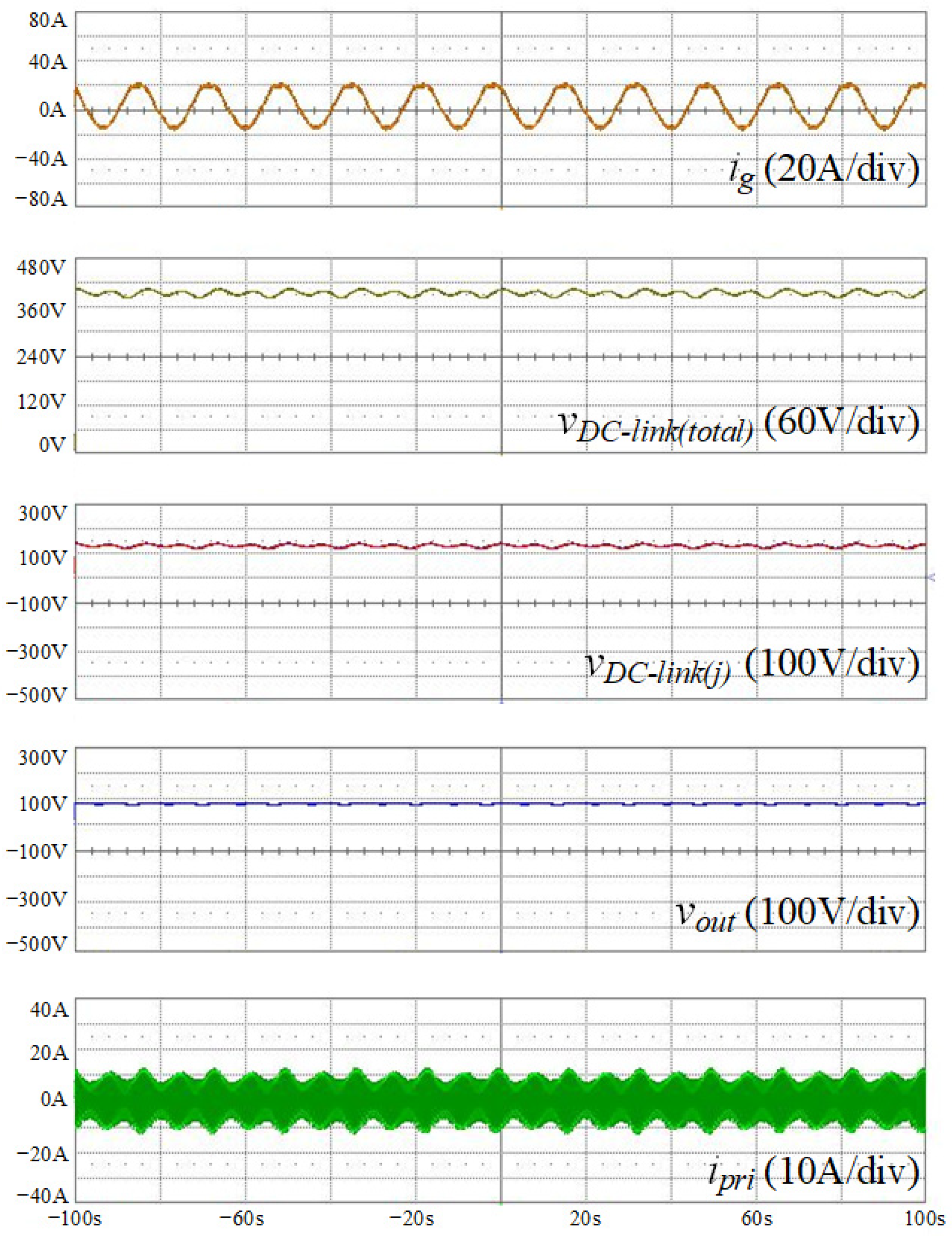
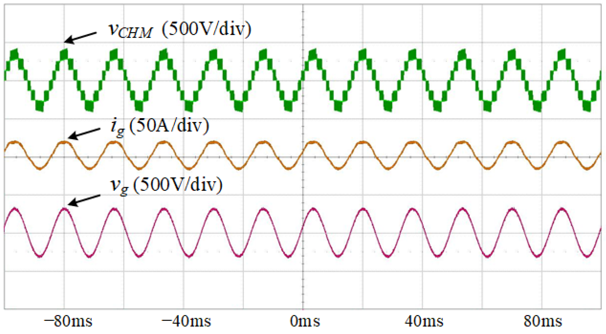
5.3. Rated Operation of the Designed SST

Figure 17 shows the enlarged waveforms of Figure 12 when the SST is operated at the rated power. Throughout the result, v o u t remains at 80 V and i g is maintained as a sinusoidal waveform with approximately 16.5 A p k . Furthermore, while v D C l i n k t o t a l is held at 390 V, v D C l i n k j is in a balanced condition to 130 V on average. Regarding i p r i , it can be noticed that a swing associated with the second order of v D C l i n k j appears.
Figure 18 shows the waveforms in relation to the CHM converter at the rated power. Note that v g and v g are in phase due to the unity power factor control. In addition, according to Table 2, since the MI is approximately 0.8, v C H M has seven levels of voltage.
In terms of DAB converter operation, Figure 19 shows the waveforms of Cell 1 at the rated power. v p r i and v s e c , the square waves with a 0.5 duty cycle, have a phase shift due to the power transmission principle of the DAB converter, as described in Section 3, inducing the trapezoid shape of i p r i . Here, a positive phase shift means the power delivery to the output of the DAB converter. It is noteworthy that v o u t is held constant without variation during the experiment.

6. Conclusions

This article proposed a hierarchical control architecture named D-CA and an operation sequence with start-up strategies for a DSP-based SST. With the proposed D-CA, because sub-boards have a dedicated DC-link voltage balancing controller for their corresponding cells individually, the computation time was distributed, resulting in a low computational burden on the master board. We presented the controller disposition to the control boards with the communication structure and sequential operation on the DSP in the time domain. Regarding the operation sequence, by arranging a step for the DC-link voltage balance prior to the entire CHM converter control, safe driving of the SST was achieved. Furthermore, considering the implementation of the DSP, start-up strategies for the CHM and DAB converters were also designed in order to prevent unexpected damage to the SST system due to a current surge. Our experimental results verified the validity of the proposed D-CA and operation sequence with start-up strategies.

Author Contributions

Conceptualization, J.-S.L. and J.J.; writing—original draft preparation, J.J.; writing—review and editing, D.C.; simulation and experiment, J.J.; supervision, J.-S.L.; project administration, D.C.; funding acquisition, J.-S.L. All authors have read and agreed to the published version of the manuscript.

Funding

This work is supported by the Korea Agency for Infrastructure Technology Advancement (KAIA) grant funded by the Ministry of Land, Infrastructure, and Transport (grant: 21RTRP-B146050-04 and RS-2021-KA163337).

Conflicts of Interest

The authors declare no conflict of interest.

References

  1. Yi, Z.; Chen, K.; Yin, L.; Wang, K. Sensing as the key to the safety and sustainability of new energy storage devices. Prot. Control Mod. Power Syst. 2023, 8, 27. [Google Scholar] [CrossRef]
  2. Ma, N.; Yin, H.; Wang, K. Prediction of the Remaining Useful Life of Supercapacitors at Different Temperatures Based on Improved Long Short-Term Memory. Energies 2023, 16, 5240. [Google Scholar] [CrossRef]
  3. Syed, I.; Khadkikar, V. Replacing the Grid Interface Transformer in Wind Energy Conversion System with Solid-State Transformer. IEEE Trans. Power Syst. 2017, 32, 2152–2160. [Google Scholar] [CrossRef]
  4. Ronan, E.R.; Sudhoff, S.D.; Glover, S.F.; Galloway, D.L. A power electronic-based distribution transformer. IEEE Trans. Power Deliv. 2002, 17, 537–543. [Google Scholar] [CrossRef]
  5. Kang, M.; Enjeti, P.N.; Pitel, I.J. Analysis and design of electronic transformers for electric power distribution system. IEEE Trans. Ind. Electron. 1999, 14, 1133–1141. [Google Scholar] [CrossRef]
  6. Bhattacharya, S.; Zhao, T.; Wang, G.; Dutta, S.; Baek, S.; Du, Y.; Parkhideh, B.; Zhou, X.; Huang, A.Q. Design and development of Generation-I silicon based Solid State Transformer. In Proceedings of the Twenty-Fifth Annual IEEE Applied Power Electronics Conference and Exposition (APEC), Palm Springs, CA, USA, 21–25 February 2010; pp. 1666–1673. [Google Scholar]
  7. Manjrekar, M.D.; Kieferndorf, R.; Venkataramanan, G. Power electronic transformers for utility applications. IEEE Ind. Appl. Conf. 2000, 4, 2496–2502. [Google Scholar]
  8. Zhao, T.; Yang, L.; Wang, J.; Huang, A.Q. 270 kVA Solid State Transformer Based on 10 kV SiC Power Devices. In Proceedings of the IEEE Electric Ship Technologies Symposium, Arlington, VI, USA, 21–23 May 2007; pp. 145–149. [Google Scholar]
  9. Wang, D.; Tian, J.; Mao, C.; Lu, J.; Duan, Y.; Qiu, J.; Cai, H. A 10-kV/400-V 500-kVA Electronic Power Transformer. IEEE Trans. Ind. Electron. 2016, 63, 6653–6663. [Google Scholar] [CrossRef]
  10. Venkat, J.; Shukla, A.; Kulkarni, S.V. Operation of a three phase solid state-Transformer under unbalanced load conditions. In Proceedings of the IEEE International Conference on Power Electronics, Drives and Energy Systems (PEDES), Mumbai, India, 16–19 December 2014; pp. 1–6. [Google Scholar]
  11. She, X.; Huang, A.Q.; Burgos, R. Review of Solid-State Transformer Technologies and Their Application in Power Distribution Systems. IEEE J. Emerg. Sel. Top. Power Electron. 2013, 1, 186–198. [Google Scholar] [CrossRef]
  12. Ge, J.; Zhao, Z.; Yuan, L.; Lu, T. Energy Feed-Forward and Direct Feed-Forward Control for Solid-State Transformer. IEEE Trans. Ind. Electron. 2015, 30, 4042–4047. [Google Scholar] [CrossRef]
  13. Lee, E.S.; Park, J.H.; Kim, M.Y.; Lee, J.S. High Efficiency Integrated Transformer Design in DAB Converters for Solid-State Transformers. IEEE Trans. Veh. Technol. 2022, 71, 7147–7160. [Google Scholar] [CrossRef]
  14. Rajendran, S.; Sen, S.; Guo, Z.; Huang, A.Q. 500 kVA Hybrid Solid State Transformer (HSST): Modelling and Control. In Proceedings of the IEEE Energy Conversion Congress and Exposition, Vancouver, BC, Canada, 10–14 October 2021; pp. 1135–1141. [Google Scholar]
  15. Busarello, T.D.; Mortezaei, A.; Paredes, H.K.; Al-Durra, A.; Pomilio, J.A.; Simoes, M.G. Simplified Small-Signal Model for Output Voltage Control of Asymmetric Cascaded H-Bridge Multilevel Inverter. IEEE Trans. on Power Electron. 2018, 33, 3509–3519. [Google Scholar] [CrossRef]
  16. Acharya, A.K.; Kumar, K.; Chowdary, K.V.; Sahu, P.K. Enhancement of Dynamic Performance of a Single Phase Cascaded H-Bridge Multilevel Inverter Using Closed Loop Controllers. In Proceedings of the 2020 International Conference on Computational Intelligence for Smart Power System and Sustainable Energy (CISPSSE), Keonjhar, India, 29–31 July 2020; pp. 1–5. [Google Scholar]
  17. Roggia, L.; Beltrame, F.; Schuch, L.; Pinheiro, J.R. Comparison between full-bridge-forward converter and DAB converter. In Proceedings of the 2013 Brazilian Power Electronics Conference, Gramado, Brazil, 27–31 October 2013; pp. 224–229. [Google Scholar]
  18. Wang, L.; Zhang, D.; Wang, Y.; Wu, B.; Athab, H.S. Power and Voltage Balance Control of a Novel Three-Phase Solid-State Transformer Using Multilevel Cascaded H-Bridge Inverters for Microgrid Applications. IEEE Trans. Power Electron. 2016, 31, 3289–3301. [Google Scholar] [CrossRef]
  19. Li, H.; Wang, Y.; Yu, C. Research on voltage balance and power balance control for three-phase cascaded multilevel converter based power electronic transformer. In Proceedings of the IECON 2016—42nd Annual Conference of the IEEE Industrial Electronics Society, Florence, Italy, 24–27 October 2016; pp. 3588–3593. [Google Scholar]
  20. Eroğlu, F.; Kurtoğlu, M.; Eren, A.; Vural, A.M. Level-Shifted Pulse Width Modulation Based Battery State-of-Charge Balancing Method for Single-Phase Cascaded H-Bridge Multilevel Converters. In Proceedings of the 2021 13th International Conference on Electrical and Electronics Engineering (ELECO), Bursa, Turkey, 25–27 November 2021; pp. 560–564. [Google Scholar]
  21. Korhonen, J.; Järvisalo, H.; Jäppinen, J.; Silventoinen, P. Level-phase-shifted pulse-width modulation for cascaded H-bridges. In Proceedings of the IECON 2022—48th Annual Conference of the IEEE Industrial Electronics Society, Brussels, Belgium, 17–20 October 2022; pp. 1–6. [Google Scholar]
  22. McGrath, B.P.; Holmes, D.G. Multicarrier PWM strategies for multilevel inverters. IEEE Trans. Ind. Electron. 2002, 49, 858–867. [Google Scholar] [CrossRef]
  23. Lee, S.Y.; Woo, M.H.; Kim, J.K.; Ryu, S.P. A novel method to improve output voltage quality of grid-connected Cascaded H-Bridge Multilevel converter with Phase-Shifted PWM and serial bus communication. In Proceedings of the 2012 IEEE Energy Conversion Congress and Exposition (ECCE), Raleigh, NC, USA, 15–20 September 2012; pp. 4513–4518. [Google Scholar]
  24. De Doncker, R.W.; Divan, D.M.; Kheraluwala, M.H. A three-phase soft-switched high-power-density DC/DC converter for high-power applications. IEEE Trans. Ind. Electron. 1991, 27, 63–73. [Google Scholar] [CrossRef]
  25. Zhou, H.; Khambadkone, A.M. Hybrid Modulation for Dual-Active-Bridge Bidirectional Converter with Extended Power Range for Ultracapacitor Application. IEEE Trans. Ind. Appl. 2009, 45, 1434–1442. [Google Scholar] [CrossRef]
  26. Cuartas, J.M.; de la Cruz, A.; Briz, F.; Lopez, M. Start-up, functionalities and protection issues for CHB-based solid state transformers. In Proceedings of the 2017 IEEE International Conference on Environment and Electrical Engineering and 2017 IEEE Industrial and Commercial Power Systems Europe (EEEIC/I&CPS Europe), Milan, Italy, 6–9 June 2017; pp. 1–5. [Google Scholar]
  27. Xiao, F.; Tu, C.; Ge, Q.; Zhou, K.; Guo, Q.; Lan, Z. Ripple Voltage Suppression and Control Strategy for CHB-Based Solid-State Transformer. IEEE J. Emerg. Sel. Top. Power Electron. 2021, 9, 1104–1118. [Google Scholar] [CrossRef]
  28. Hannan, M.A.; Ker, P.J.; Lipu, M.S.; Choi, Z.H.; Rahman, M.S.; Muttaqi, K.M.; Blaabjerg, F. State of the Art of Solid-State Transformers: Advanced Topologies, Implementation Issues, Recent Progress and Improvements. IEEE Access 2020, 8, 19113–19132. [Google Scholar] [CrossRef]
  29. Bhawal, S.; Chakraborty, S.S.; Hatua, K. Dynamic Modeling and Closed-Loop Control of a Solid-State Transformer (SST) Based on Series Resonant Converter (SRC). IEEE J. Emerg. Sel. Top. Power Electron. 2022, 10, 3733–3745. [Google Scholar] [CrossRef]
  30. Xu, W.; Guo, Z.; Vetrivelan, A.; Yu, R.; Huang, A.Q. Hardware Design of a 13.8-kV/3-MVA PV Plus Storage Solid-State Transformer (PVS-SST). IEEE J. Emerg. Sel. Top. Power Electron. 2022, 10, 3571–3586. [Google Scholar] [CrossRef]
  31. Saeed, M.; Cuartas, J.M.; Rodríguez, A.; Arias, M.; Briz, F. Energization and Start-Up of CHB-Based Modular Three-Stage Solid-State Transformers. IEEE Trans. Ind. Appl. 2018, 54, 5483–5492. [Google Scholar] [CrossRef]
  32. Behera, R.K.; Ojo, O. Modeling and control of DAB converter for solar micro-grid application. In Proceedings of the 2015 6th International Conference on Power Electronics Systems and Applications (PESA), Hong Kong, China, 15–17 December 2015; pp. 1–5. [Google Scholar]
Figure 1. Topology configuration of 3-cell SST. (a) CHM converter; (b) DAB converter.
Energies 16 06095 g001
Figure 2. Control block diagram of CHM.
Energies 16 06095 g002
Figure 3. Control block diagram of DAB. (a) Output voltage controller; (b) DC-link voltage balancing controller.
Energies 16 06095 g003
Figure 4. The disposition of controllers and data transfer of communication in D-CA.
Energies 16 06095 g004
Figure 5. The operation of D-CA in the time domain with respect to DSP, including carriers, signals, computation time, and communications.
Energies 16 06095 g005
Figure 6. Waveforms of the operation sequence of designed SST based on D-CA.
Energies 16 06095 g006
Figure 7. Omission of switching pulses in CHM with and without the applied start-up strategy. (a) Without the start-up strategy; (b) with the start-up strategy.
Energies 16 06095 g007
Figure 8. Difference between ipri and isec in DAB with and without the applied start-up strategy. (a) Without the start-up strategy; (b) with the start-up strategy.
Energies 16 06095 g008
Figure 9. The PWM error caused by the delay from the shadow register.
Energies 16 06095 g009
Figure 10. Experimental setup.
Energies 16 06095 g010
Figure 11. The waveforms of D-CA operation corresponding to Figure 5.
Energies 16 06095 g011
Figure 12. The experimental results corresponding to Figure 6, displaying the entire operation sequence of the designed SST. (i) PLL (ii) pre-charge of DC-link capacitors (iii) pre-charge of output capacitors (iv) DC-link voltage balancing and output voltage control (v) DC-link voltage control (vi) increase of the output voltage to rated value.
Energies 16 06095 g012
Figure 13. The enlarged waveforms of DC-link voltages in (iii) and (iv) showing the performance of the DC-link voltage balancing controller.
Energies 16 06095 g013
Figure 14. The experimental results of the designed SST when load changes to (a) 12.5%, (b) 25%, and (c) 50% of the rated load.
Energies 16 06095 g014
Figure 15. Experimental results: the switching pulses in the CHM validating the start-up strategy.
Energies 16 06095 g015
Figure 16. Experimental results: The switching pulses in the DAB primary side validating the start-up strategy. (iii) pre-charge of output capacitors (iv) DC-link voltage balancing and output voltage control.
Energies 16 06095 g016
Figure 17. The experimental results of the designed SST at the rated load.
Energies 16 06095 g017
Figure 18. Experimental results showing steady state of CHM at rated load.
Energies 16 06095 g018
Figure 19. Experimental results showing steady state of DAB at rated load.
Energies 16 06095 g019
Table 1. Differences between conventional methods and this article.
ReferencesIntroduction of Overall Control SequenceCommunication Structure DescriptionControl Hierarchical Architecture Description
[26]PresenceNoneNone
[27]PresenceNoneNone
[28]NoneNonePresence
[29]NoneNonePresence
[30]PresenceNonePresence
[31]PresenceNonePartially presence
(without a balancing control)
Table 2. Experiment parameters.
ParameterValue
Rated power of SST2.56 kW
Input grid voltage220 Vrms, 60 Hz
DC-link voltage of CHM390 Vdc
Output voltage of DAB80 Vdc
Input AC filter inductor1.9 mH
Capacitance of 1 cell DC-link1175 μF
Capacitance of DAB converter2350 μF
Switching frequency of CHM1.67 kHz
Switching frequency of DAB10 kHz
Control frequency5 kHz
Turn ratio of MFTR1.5:1
Rated output voltage80 V
Disclaimer/Publisher’s Note: The statements, opinions and data contained in all publications are solely those of the individual author(s) and contributor(s) and not of MDPI and/or the editor(s). MDPI and/or the editor(s) disclaim responsibility for any injury to people or property resulting from any ideas, methods, instructions or products referred to in the content.

