2.1. Previous Work
The CLLC is an extension of the LLC circuit topology [
27] that uses the “first harmonic approximation” (FHA) technique to enable the analysis of resonant converters by means of a classical complex AC circuit analysis. In order to reduce the complexity of the analysis, an earlier version of a half-bridge CLLC DC–DC converter circuit was presented by Zou et al. [
28]. They specifically defined the voltage source on the primary side as the grid voltage and the battery on the secondary side to be the vehicle battery. When the magnetization current and the core loss of the transformer are ignored, the circuit mode can be simplified, as shown in
Figure 1; it consists of two capacitors on both the grid side, simplified by a voltage source
Vin, and the vehicle side, simplified by an output resistance
Ro. However, in the circuit model, there are multiple conducting paths of circulating current in the secondary side, as it has two capacitors. If the gate pulse of
M4 achieves zero-current switching (ZCS) early, the secondary-side resonant current partially circulates through
M4, discharging the battery, which lowers the conversion efficiency. Therefore, in order to minimize the circulating current in the secondary side, an extra dead-band control is necessary to ensure the zero crossing of the resonant current occurs within the dead time. This made the control system dependent on the loading condition while charging or discharging. The dead time needs to be long enough for handling the worst case within the desired switching frequency range; however, the increase in the dead time lowers the power conversion efficiency and the regulation in constant voltage control.
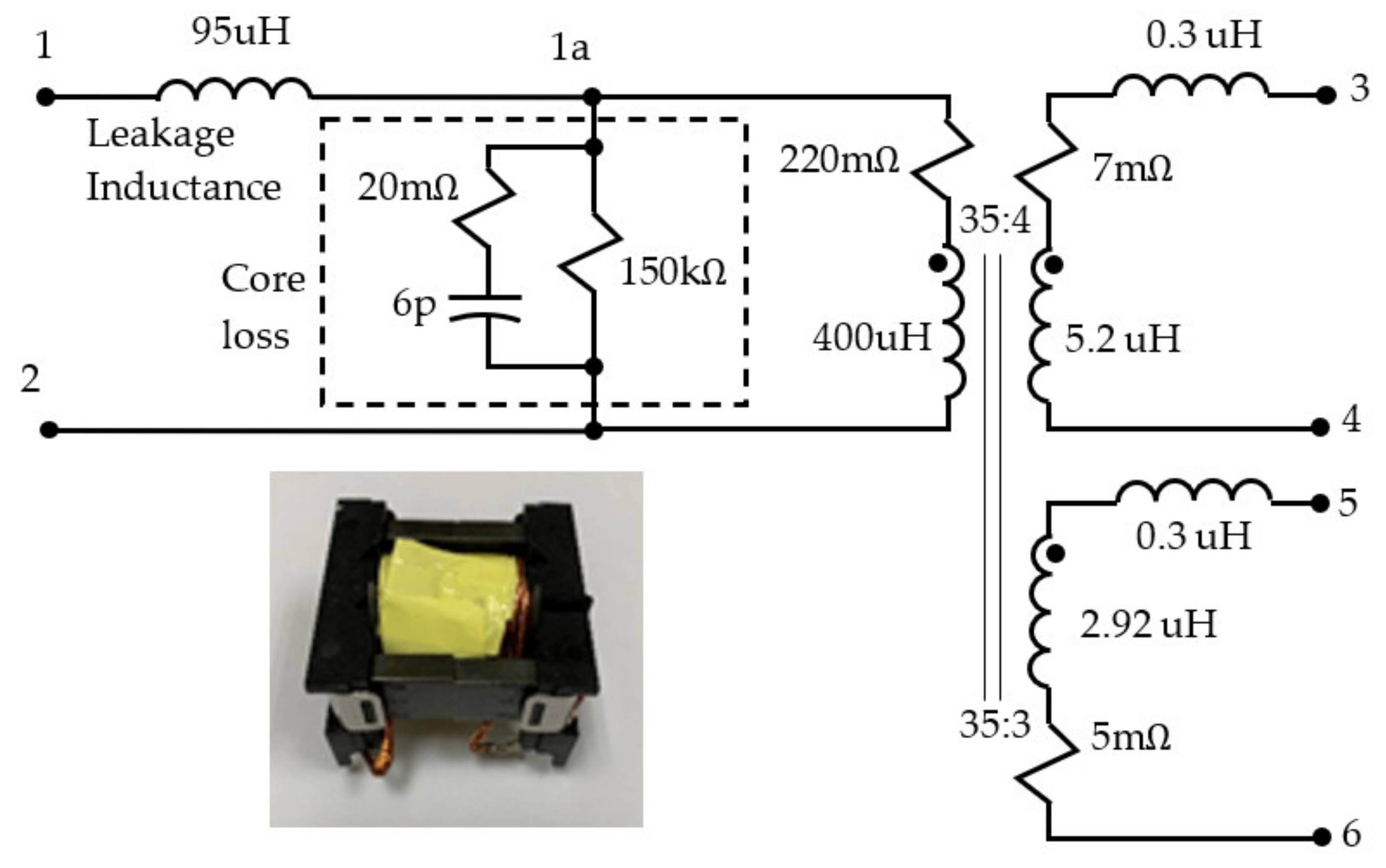
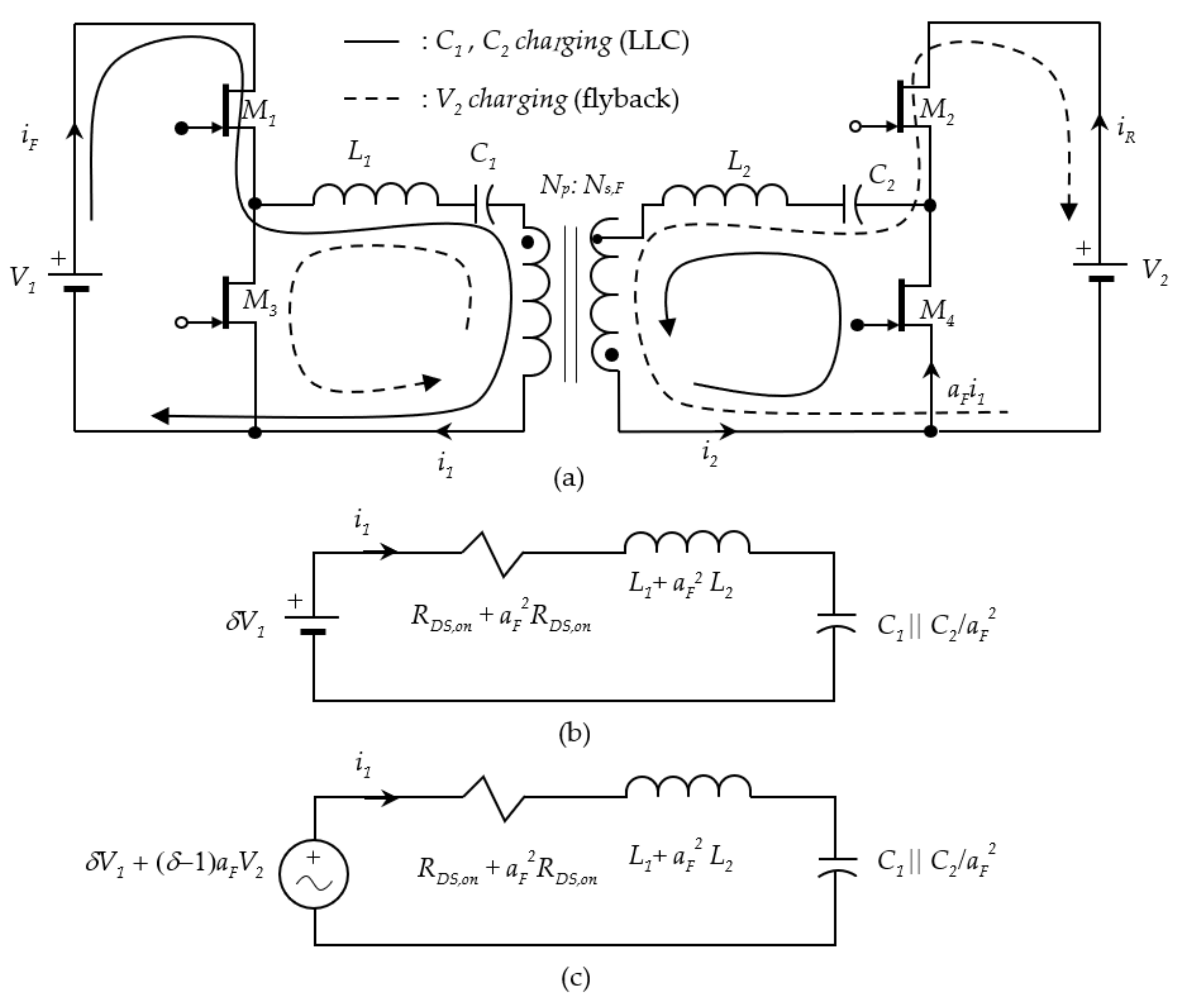
2.3. Transformer Model
Reducing the magnetization current is necessary to improve the efficiency of the CLLC circuit and simplify its model into a second-order oscillation system. The magnetization current, which is not directly related to the power rating, can significantly impact the CLLC power-conversion efficiency. The switching frequency is used to match the series resonance, accounting for environmental changes, LC component variation, and stray impedance. By using a simple second-order resonant model, the duty cycle can be easily adjusted to achieve ZCS (zero-current switching) and further enhance the power conversion efficiency. The Steinmetz equivalent circuit, as shown in
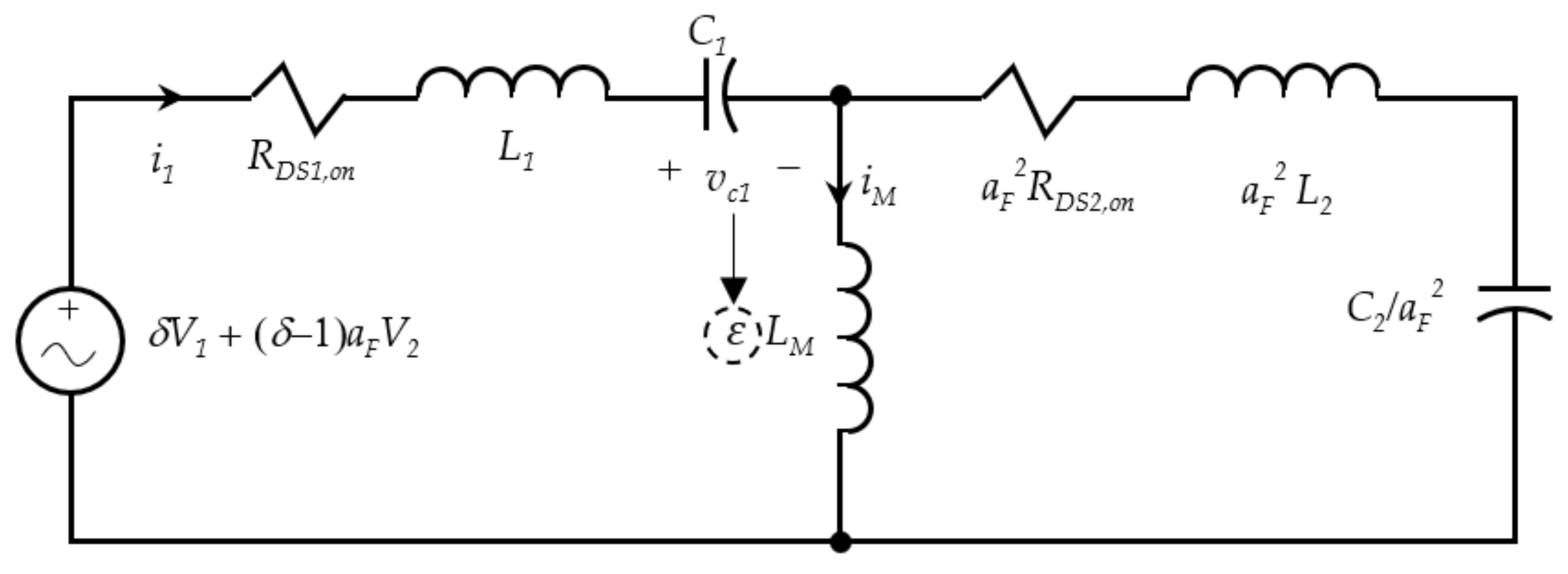
Figure 4, is a practical representation of a transformer’s physical behavior through an equivalent circuit model incorporating an ideal transformer. Ignoring the core loss of the transformer due to the air gap introduced into the transformer core design, the magnetizing inductance is still present between two LC tanks and results in a fourth-order system that consists of both series resonance and parallel resonance. The equivalent circuit model of the half-bridge CLLC is shown in
Figure 5. In this paper, we used
to denote the transformer turn ratio in the forward (charging) mode,
to denote the transformer turn ratio in the reverse (discharging) mode, and
to denote the nominal transformer turn ratio. A nominal turn ratio with
can only result an internal series resonance with no current flowing in any charging direction. The half-bridge CLLC circuit uses the turn ratio
during the forward (charging) mode and the turn ratio
during the reverse (discharging) mode.
The LC tank’s series resonance on both sides of the transformer is identical, allowing for the use of a single switching frequency to produce the series resonance on both sides of the transformer.
For the series resonance design, the nominal transformer turn ratio
was used to determine both the inductance and capacitance ratios and to keep the inductors and capacitors the same without replacement in different (charging/discharging) modes. In that case, the magnetization current
from the circuit shown in
Figure 5 can be ignored. The switching frequency
is preferable to match the series resonance of the LC tank on both sides of the transformer.
Considering that the magnetization current
can or cannot be ignored from the equivalent circuit, we first assumed the switch frequency is tuned to eliminate the series impedance of the LC tank, and the remaining switch resistance
was used to compare with the magnetization inductance as follows. As shown in
Figure 5, the on-resistance
of transistors is outside of the LC tank when the transformer is inside of the LC tank. Therefore, when the perfect series resonance is assumed, the AC voltage experienced by the on-resistance
is equivalent to the difference between the input voltage and the transformed output voltage as
, which is much smaller than that of the transformer coils which oscillates with the capacitor voltage
with peak-to-peak voltage swing
. Therefore, a correction factor
for the forward (charging) mode was introduced to equalize the different voltages in one equivalent circuit.
The magnetization current is a branch current derived from the current divider circuit consisting of magnetization inductance and the switch on-resistance as follows.
The inductance
is the primary inductance, excluding the leakage inductance during the forward (charging) mode. Similarly, the magnetization current required in the reverse (discharging) mode can also be expressed as follows.
Since the turn ratio between the primary winding and the secondary winding becomes
in the reverse (discharging) mode, the magnetization inductance ratio between the forward (charging) mode and the reverse (discharging) mode is expressed in the reverse (discharging) mode as follows.
Equation (5) can be re-written as follows.
Equation (7) states that the resistance of in the similar range of ignores magnetization. High-breakdown-voltage GaN HEMTs were applied to the CLLC as and , and the low-resistance GaN HEMTs were applied as and . It was a challenging task for the high-breakdown-voltage GaN transistor to have a low resistance. According to Equation (7), we need only a high to balance the resistance between high-/low-voltage GaN. The task for reducing the effect of the magnetization current from the CLLC circuit analysis is then transformed into the task of increasing , as shown in Equations (5) and (7). In order to achieve this, we need to (1) use the higher turns of the coils on both of the primary and secondary windings to increase both and and (2) increase the switching frequency . The latter solution has a side effect: the switching loss can also be amplified due to a high switching frequency. The former solution has also a side effect, which is that it increases the transformer size. A hybrid solution was adopted in which we increased both the turns and the switching frequency to their limits.
If the magnetization current can be ignored through the use of low-resistance GaN HEMTs, the series resonant circuit can then be simplified by combining both the inductances and the capacitances into a single inductor and single capacitor. The resonance mechanism can be simplified into a secondary differential equation, which is useful for the forward (charging) and reverse (discharging) mode analysis in the following sections.
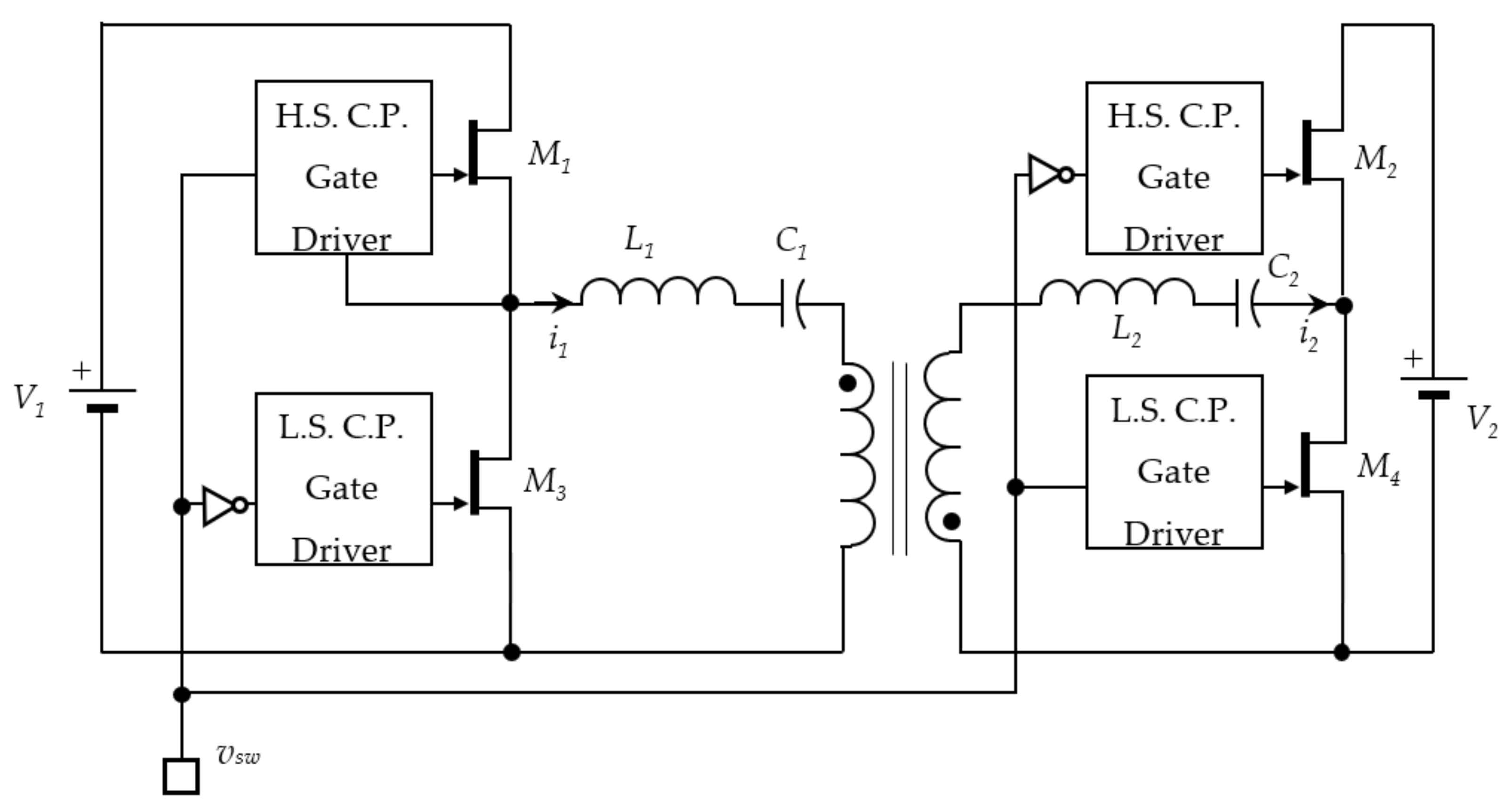
2.4. Forward (Charging) Mode
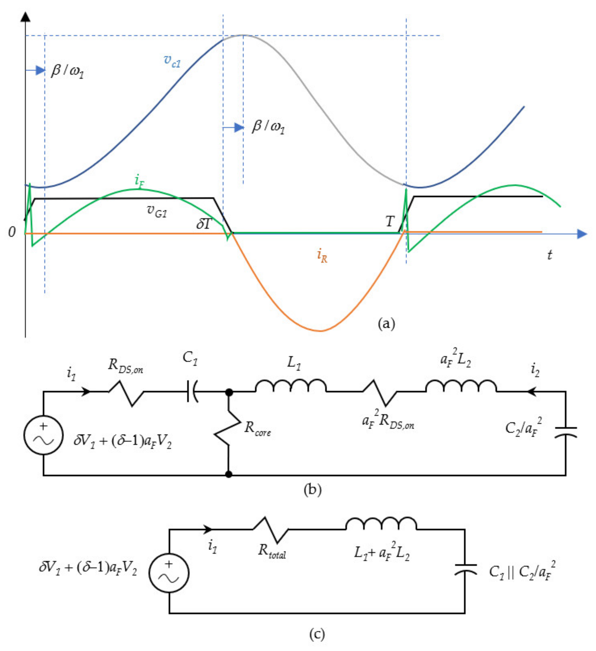
As shown in
Figure 6a, there are two sessions for the charging mode. The first session, indicated by a solid line, is for charging the resonant capacitors
C1 and
C2 during the turn-on time of transistors
M1 and
M4. The second session, indicated by a dash line, is for transferring the electrical energy stored in both
C1 and
C2 to the battery
V2 on the secondary side during the turn-on time of transistors
M2 and
M3. During the second session, the same resonant voltage on
C1 must be transformed using the transformer into a voltage level higher than
V2 in order to yield a charging current flow into the battery
V2; therefore, we used the turn ratio
.
The equivalent model from the circuit as shown in
Figure 6a can be converted into either
Figure 6b or
Figure 6c depending on the view of the DC component and the AC swing analysis, respectively. The DC component and AC swing analyses both share the same series RLC circuit topology, which are different only in the source type and the mismatched loop resistance. The magnetization inductance was assumed to be considerably large and can be ignored in the analyses. Ignoring the core loss, parasitic capacitance of the coils of the transformer, and magnetization current, we can simplify the CLLC circuit when
vsw is high by assuming that the coupling coefficient of the transformer is the unity.
The equation above is applicable for both DC component and AC swing analyses, because the voltage source vanishes. The Heaviside step function
sets the time as zero when
M1 and
M4 turn on. In Equation (8), the natural frequency
is a function of primary inductor
L1 that can simply be the transformer leakage inductance, the secondary inductance
L2 that can also be the secondary leakage inductance, and primary capacitor
C1 or the secondary capacitor
C2. The transformer turn ratio
during the forward mode is expressed as follows.
denotes the turns on the primary winding and
denotes the turns on the secondary winding of the transformer windings in the forward (charging) mode. The natural frequency
is then defined as follows.
The natural frequencies in Equation (10) can be simplified when the following conditions are satisfied.
Equation (11) then yields the relation that eliminates both factors
and
as follows.
denotes the base frequency, and the impedance on both sides of the transformer vanishes under the base-frequency switching condition.
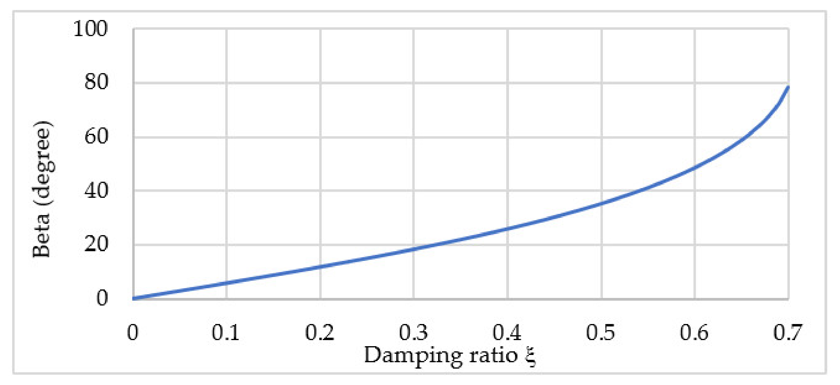
The damping ratio
of the current oscillation is derived as follows, providing that the transistor on-resistances are identical.
The series resonant quality factor is derived as follows.
Equation (8) shows that the damping ratio and series resonant quality factor of the circuit are a function of Rayleigh energy dissipation in the second-order term of the RHS. In Equation (14), we modeled only the resistive loss of the transistor as the energy dissipation source, which is not entirely accurate when the drain–source voltage is high during turn-off. The reverse recovery charge Qrr stored in the output parasitic capacitance Coss of the transistor can produce a larger energy dissipation than the resistive loss.
To address this issue, using the GaN HEMT instead of MOSFET or IGBT can be beneficial because the
Coss of a GaN HEMT is only one tenth of that of the MOSFET or IGBT. This can result in a very small switching loss compared to the resistive loss under 250 kHz switching frequency. The damping ratio and quality factor of the series resonant circuit is calculated as shown in
Table 1, according to Equations (14) and (15).
When the on-resistances of the transistors are in the range of 100 mΩ, the capacitance of
C1 is in the range of pF, and the inductance is 100 μH. The damping ratio is very small for a turn ratio
aF lower than 10, making the system in Equation (8) lightly damped or even undamped. In the perfect tuning of the resonance, the initial condition of the current
i1(0) is zero; provided there is still some charge remaining in the capacitors
C1 and
C2, the current response can then be expressed as follows.
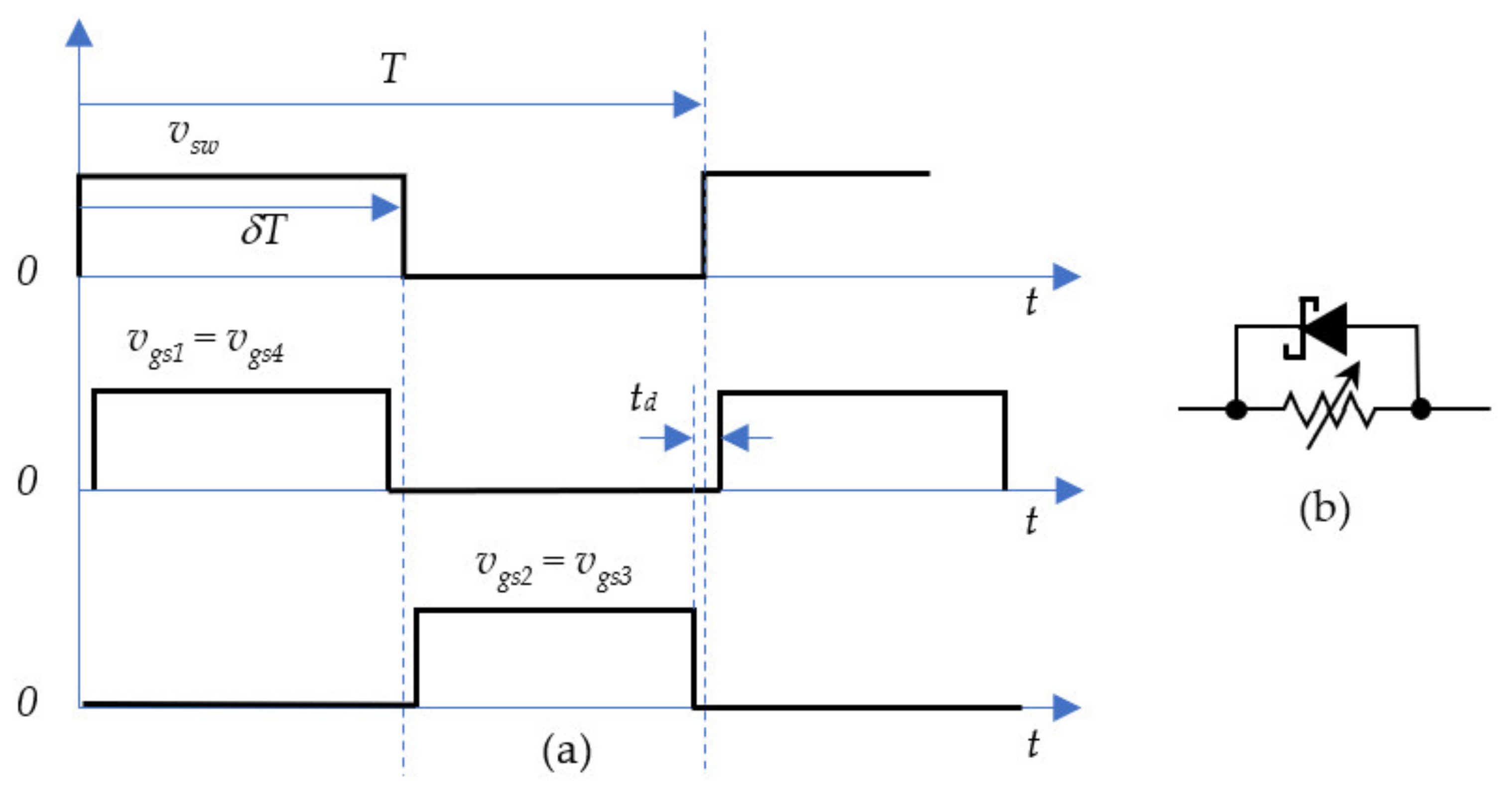
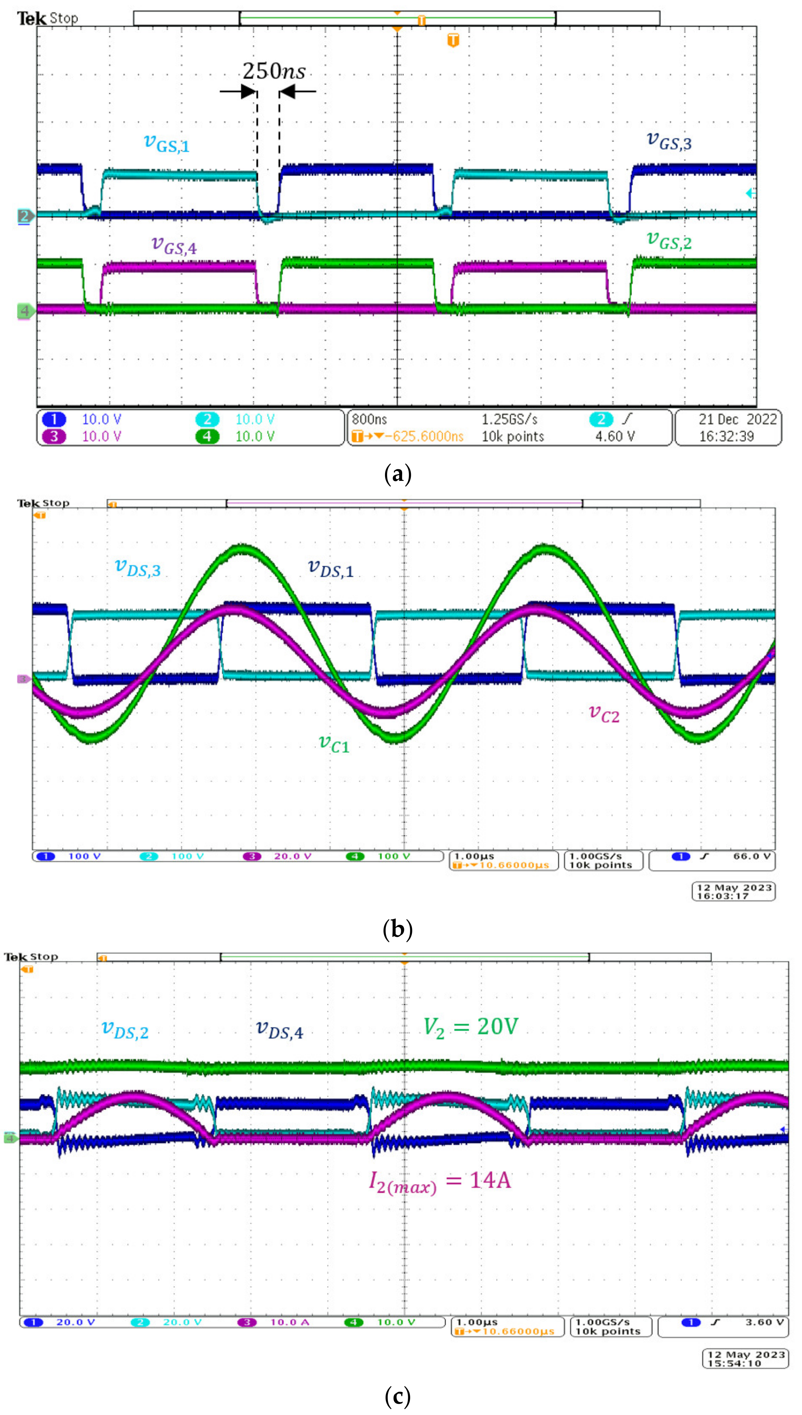
The phase lag between the switching time and the zero-current time is dependent on both the switching frequency and the duty cycle δ of the switching control. The ideal switching operation is when the current becomes zero at ; under the current resonance, the current on the inductor L2 located on the secondary side of the transformer is also zero. At the same time, the capacitors C1 and C2 are filled with their maximum charges, and both reach the highest voltage under the LC resonance. This is, then, the best moment to turn off the transistors M1 and M4 as well as turn on transistors M2 and M3 to achieve the zero-current switching (ZCS) operation, which yields . If the switching performed a perfect ZCS, the switching frequency of the transistors must be identical to the resonance frequency of the LC tank.
As a result, as shown in
Figure 7, the voltage
is able to swing from
as its minimum voltage at time
to the maximum voltage
at time
. The capacitor voltage swings on a bias voltage
, which is the DC component that depends on the duty of the transistor switching control, as shown in
Figure 7. The reason for the bias voltage to exist is that the capacitor is subjected to an average voltage due to the input voltage
under the switching operation, as shown in
Figure 6b. The capacitor voltage may be written as follows.
denotes the peak-to-peak voltage, which is obtained as follows.
We can obtain the voltage on the same capacitor
C1, holding a relation in the middle time
, as follows.
The maximum current on the primary side is then obtained as follows.
The power transferred from the primary-side grid battery to the capacitors during the first session of the charging mode when the transistors
M1 and
M4 turn on can be derived for the primary side as follows.
The peak-to-peak voltage
was determined by the series resonance quality factor
, which can be directly measured from the experiments or obtained through simulation. As shown in
Figure 6c, the switching of AC voltage is based on the voltage difference between the grid DC voltage and the vehicle DC voltage during the entire forward mode as follows.
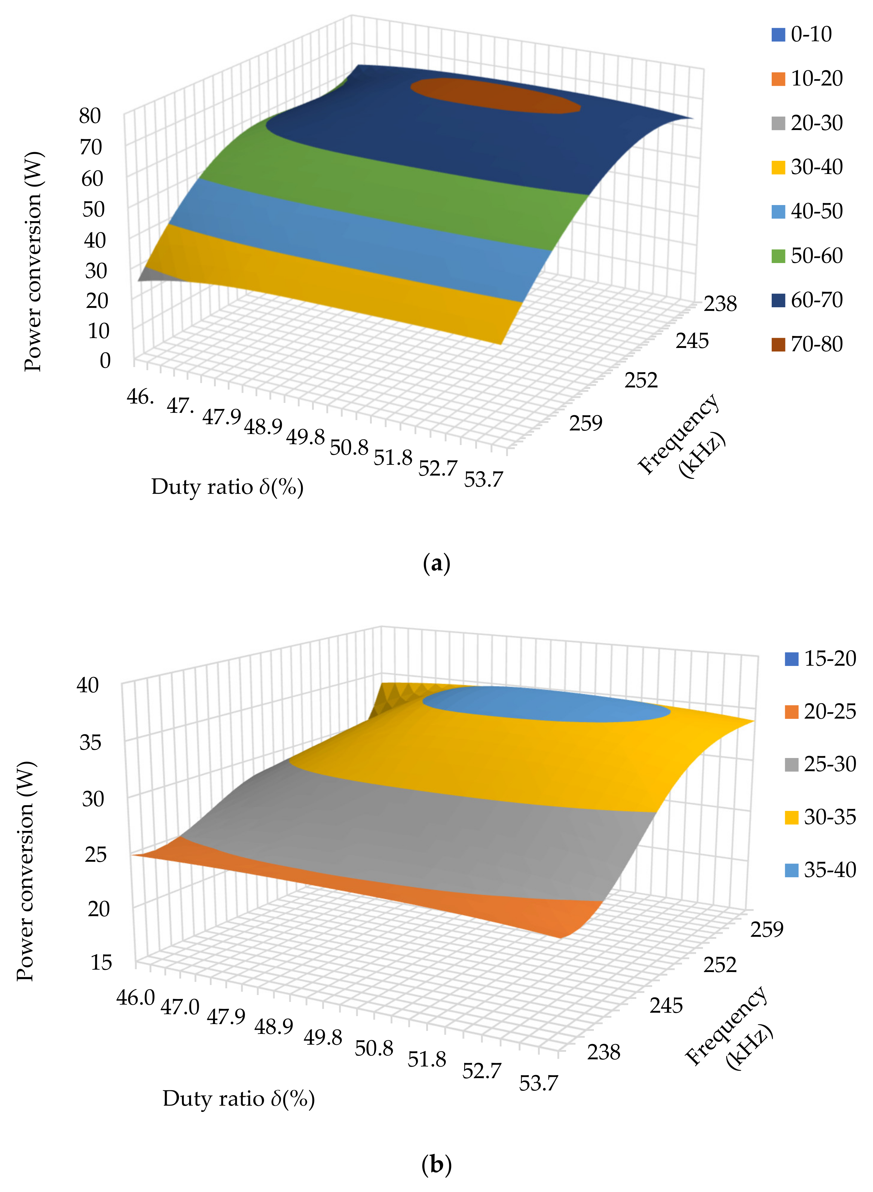
According to Equation (22), the output power can increase by increasing the capacitance and reducing the primary leakage capacitance simultaneously, without changing the switching frequency. The output power of a particular design was calculated as shown in
Table 2.
2.5. Reverse (Discharging) Mode
As shown in
Figure 8a, there are also two sessions for the discharging mode. The first session with a current flow indexed using a solid line is to charge the resonant capacitors
C1 and
C2 during the turn-on time of transistors
M2 and
M3. The second session is to convey the increased electrical energy stored in both
C1 and
C2 into the battery
V1 on the primary side during the turn-on time of transistors
M1 and
M4, whose current path is marked as a dashed line. Depending on DC component and AC swing analyses, the circuit depicted in
Figure 8a can be converted into either
Figure 8b or
Figure 8c. The transformer turn ratio between the primary side and secondary side during the reverse mode is provided as follows.
denotes the turns on the primary winding and denotes the turns on the secondary winding of the transformer windings in the reverse (discharging) mode.
Analogous to Equation (14), the damping ratio
of the current
i2 oscillation is derived as follows, providing that the transistor on-resistances are identical.
The series resonant quality factor is derived as follows.
The damping ratio and quality factor of the series resonant circuit was calculated as shown in
Table 3, according to Equations (24) and (25).
Analogous to Equation (25), the maximum current on the secondary side due to the switching frequency
is then obtained as follows.
The power transferred from the secondary side battery to the primary capacitor during the first session of the charging mode, when the transistors
M2 and
M3 turn on, can be derived for the secondary side as follows.
The peak-to-peak voltage
is determined by the series resonant quality factor
, which is derived as follows. As shown in
Figure 8c, the switching of the AC voltage is based on the voltage difference between the grid DC voltage and the vehicle DC voltage during the entire forward mode as follows.
The series resonant quality is crucial to the power conversion rate. The higher the series resonant quality, the higher the peak-to-peak voltage
in capacitor
. According to Equation (24), we may select a very-low dynamic RON resistance to reduce the damping ratio and increase the series resonant quality. This yields a reason for the GaN HEMT to be used when it is known that the electron mobility of 2DEG of AlGaN/GaN is high and the resistance of the GaN HEMT can be made very low. The calculation of the output power of a particular design is shown in
Table 4. Comparing the results of
Table 2 with that of
Table 4, we can find that the charging power to the vehicle during the charging mode is almost as twice the discharging power from the vehicle. The difference can be made smaller by redesigning the transformer turn ratio.


 ,
, 


