Article

A Hybrid Switched-Inductor/Switched-Capacitor DC-DC Converter with High Voltage Gain Using a Single Switch for Photovoltaic Application

1
Department of Electrical Engineering, Faculty of Engineering, Arak University, Arak 3848-7-6941, Iran
2
Department of Electrical Engineering, Kermanshah Branch, Islamic Azad University, Kermanshah 67198, Iran
3
Centre for Smart Power & Energy Research, School of Engineering, Deakin University, Waurn Ponds, VIC 3216, Australia
4
Centre for Clean Energy Technologies and Practices, Queensland University of Technology, Brisbane, QLD 4000, Australia
*
Authors to whom correspondence should be addressed.
Energies 2023, 16(14), 5524; https://doi.org/10.3390/en16145524
Submission received: 11 May 2023 / Revised: 26 June 2023 / Accepted: 18 July 2023 / Published: 21 July 2023
(This article belongs to the Section A2: Solar Energy and Photovoltaic Systems)

Abstract

:
This paper introduces a new high-step-up, non-isolated switched-inductor switched-capacitor DC-DC converter. The proposed converter remarkably integrates switched-capacitor and switched-inductor cells, leading to a significant increase in voltage gain. This unique composite structure not only ensures the continuity of input current, but also successfully minimizes the current ripple and voltage stress across the components, thereby optimizing efficiency. The standout feature of this converter is its singular switch controlled by pulse-width modulation (PWM), which simplifies its operation. A rigorous steady-state operation analysis is conducted, providing a comprehensive understanding of the converter’s performance. For validating the theoretical findings, the paper also details a real-world prototype of the converter. Comparative studies conducted with other similar structures substantiate the superiority of the proposed converter.

1. Introduction

Today, high step-up DC-DC converters are used to increase low voltage sources to high output voltage for renewable energy applications. In a grid-connected PV system, the voltage level, which is generated by PV arrays cannot be used to feed the grid-connected side. In fact, low input voltage should be boosted with high voltage gain. Hence, high-step-up DC-DC converters are presented for use as an interface circuit between low-voltage PV arrays and high-voltage grid-connected sides [1,2]. DC-DC boost converters are the best topology in comparison with others for these applications. However, boost converters will be unstable when their duty cycle reaches unity. In other words, the voltage gain of boost converters is limited. Furthermore, using a high duty cycle creates lots of problems, such as low efficiency, high conduction/switching losses, high reverse recovery, and high electromagnetic interference (EMI). Moreover, the selection of high-voltage components, the equivalent series resistance of components, and the stability issue are three main limitations of high voltage gain [3,4]. By adjusting the transformer turn ratio in isolated converters, high voltage gain can be achieved. However, since transformers inherently possess leakage inductance, these topologies can generate high voltage spikes and substantial power losses [5]. Therefore, either a novel snubber is required, or a high voltage may be obtained in non-isolated quadratic gain [6,7]. Due to galvanic isolation, the isolated converters are typically employed in high-power applications or for sensitive loads [8]. To eliminate the leakage inductance, non-isolated DC-DC converters are used in many medium and low-power applications. Moreover, they have a lower size, cost, weight, volume, and higher efficiency in comparison with isolated types. Furthermore, they share common ground for both sides at the input and the output [9]. Non-isolated converters can be categorized as coupled-inductor type and non-coupled-inductor type. In fact, coupled-inductor types are introduced to solve the problems associated with transformers. However, this type needs an accurate calculation to design a coupled magnet [10]. It is obvious that the non-coupled-inductor type has a lower number of magnetic elements and a smaller size compared to the coupled-inductor type. Different methods, such as coupled inductors [11,12], switched inductors and switched capacitors [13,14,15,16,17,18,19], input-parallel-output series connection, stacked converters [20], and cascaded structures [21], can be employed to achieve high voltage gain in non-isolated converters. However, they suffer from low efficiency due to high voltage stress across switches for coupled inductors and switched inductor cells [22], or due to a large number of elements for cascaded structures, stacked converters, and switched-capacitor cells [23]. Integrating some of the different voltage lift methods, such as switched capacitors, switched inductors, coupled inductors, or multiplier cells is an efficient way to reach high gain. High voltage gain with a low duty cycle in switching-mode DC-DC converters is reached by applying multiple capacitors. The operation of the converter shows that the proposed method leads to high efficiency. A boost converter that is utilized as a switched capacitor is proposed in [24]. However, the converter has a low efficiency at constant voltage. Many other topologies have used switched capacitors to increase voltage gain in non-isolated DC-DC converters [25]. On the other hand, many switched-inductor methods use a high number of cells to reach a high voltage gain in their proposed converters [26]. However, most of them have complex structures. Many different topologies for high-step-up non-isolated DC-DC converters with a single switch are presented in the literature [27,28,29,30]. Most of them use one switch and three diodes as the active elements in their structure. The voltage gain of all aforementioned topologies is limited to ten. The proposed converters with a single switch in [3,31] comprise two inductors, four diodes, and capacitors. They suffer from high conduction losses due to the high number of components. A modified switched inductor network is used in [17] to increase the voltage gain. The proposed converter needs extra diodes and inductors, which leads to low efficiency. A cascaded boost converter with a low number of elements is presented in [28,29,32]. In these topologies, high voltage gain is achieved when the duty cycle is 0.8. To reach high-step-up operation in a lower-duty cycle, a network consisting of two capacitors and diodes is applied in [33]. Moreover, a switched-capacitor network is used in [34] to increase the voltage gain further. Additionally, a family of step-up DC-DC converters that use switched-capacitor inductor cells to achieve high voltage gain is presented in [15,35]. Most of them have a high number of components in their structure, which leads to low efficiency.
In this paper, a new high-step-up converter based on switched capacitors and switched inductors is proposed, which has the following characteristics compared to similar structures.
  • Only one switch is used in the proposed topology. Therefore, this converter has much less complexity compared to similar structures.
  • This converter has only two operation modes. This operation is based on a conventional boost converter. The proposed converter has a linear operation.
  • The control of this converter is PWM. Due to the single-switch structure, the design of the feedback circuit and gate driver is much simpler compared to similar structures.
  • This converter has a very high reliability factor for use in various applications due to its simple structure and linear operation.
  • This converter has a very high voltage gain (G = 23), which is suitable for many industrial applications. This high gain is due to the use of stacked cells of switched inductors in the input section, and switched capacitors in the output section.
  • In the input section, the converter consists of two integrated cells of switched inductors, which have the following advantages:
    The properties of the basic boost converter are preserved in the operation of the proposed topology.
    When the switch is turned on, the energy is stored in the switched inductors. Besides, this energy is transferred to the output when the switch is turned off.
    These two cells are merged, and the number of energy storage elements is reduced. This reduces the order of the proposed circuit and improves the stability of the converter.
    These cells of the integrated switched inductors have the role of the input filter inductor in the conventional boost converter, which causes the input current to be non-pulsating. As a result, the current stress of the elements is improved.
    By dividing the input current in the input inductors (similar to the interleaved structures), the current stress of diodes and the Ohmic losses in the paths are reduced. Therefore, less heat is produced in the converter, and there is no need to use a heat sink for switches and diodes at high powers.
  • This converter uses a cell of switched capacitors in the output part of the converter. This cell has the following advantages:
    This cell has a capacitive characteristic and creates an inherent voltage isolation between the input and the output. Hence, the converter does not need an isolating transformer.
    This cell also has the role of increasing the voltage. It stores energy when the switch is turned on. Then, it transfers the energy to the output when the switch is turned off.
    This cell creates two parallel paths for transferring power from input to output, which makes the converter very suitable for high-power applications.
    Due to being in series with the output part of the converter, this cell of the switched capacitor reduces the output voltage ripple. However, the output filter of the converter is a first-order filter.
In order to accurately investigate the proposed converter, the remainder of this paper is organized as follows. The proposed topology is presented in Section 2; the principle of operation is explained in detail in Section 3. Design considerations and the related formulas are considered in Section 4. The experimental results and their analysis are provided in Section 5. The conclusion is presented in the Section 6.

2. Circuit Configuration of the Proposed Converter

The proposed converter is shown in Figure 1. As can be seen from this figure, the proposed converter has only one switch. Inductors L1, L2, and L3 are input inductors. Moreover, capacitors C1 and C2 are input capacitors in the proposed high-step-up converter. In this circuit, CO and RL are the output capacitor and the output resistor, respectively. The complexity of the operation and control of a converter is directly related to the number of switches and diodes. This increment occurs because each switch requires a gate drive signal to control it. As can be seen from the proposed structure, only one switch is used, which makes the converter operation much simpler than similar topologies.
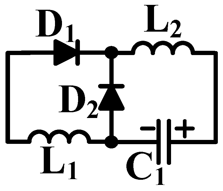
The proposed step-up cell is a combination of a switched inductor and switched capacitor, as shown in Figure 2. To increase the output voltage level, this cell is used twice in the circuit.
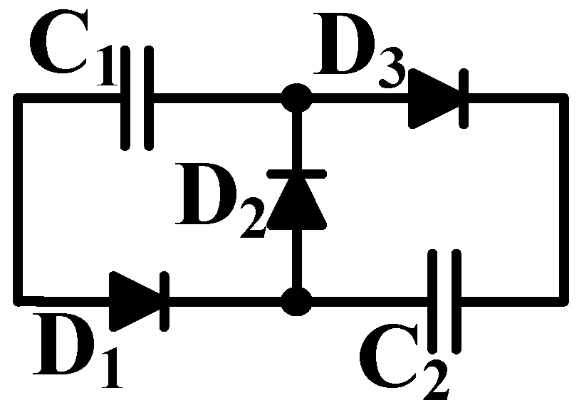
The basic structure of the proposed topology is a boost converter. At the output, a switched-capacitor cell is used instead of the output diode to increase the voltage gain. The switched-capacitor cell is depicted in Figure 3.

3. Analysis of Operation Modes

In this section, the performance of the proposed high-step-up converter in different modes is explained. For simplicity of circuit analysis, the following assumptions are considered as follows.
  • The output capacitor is large enough that the voltage across it can be considered a constant voltage.
  • All circuit elements are considered ideal.
  • The converter operation is analyzed in a steady-state condition.

3.1. CCM Operation

The proposed converter has two operating modes. The equivalent circuit for each mode and the theoretical waveforms are shown in Figure 4 and Figure 5, respectively.
Interval 1: (t0 − t1) [see Figure 5a]: This mode starts when switch S is turned on at t0. Before t0, it is assumed that the voltage across capacitor C1 is twice the input voltage and VC2 is equal to the input voltage. As well, voltage capacitors VC3 = VC4 are considered equal to half the output voltage. According to (1), the voltage across inductor L1 is positive during this mode. Therefore, the current passing through the inductor increases linearly.
V L 1 = V S + V C 1 + V C 2
V C 2 t 0 = 1 2 V C 1 t 0 = V S
So;
V L 1 = 4 V S
Δ I L 1 = 4 V S L 1 t 1 t 0 = 4 D V S L 1 f s
During this mode, energy is transferred from the input source and capacitors C1 and C2 to inductor L1. Moreover, the voltage across inductor L2 can be calculated as follows.
V L 2 = V S + V C 2 = 2 V S
Δ I L 2 = 2 V S L 2 t 1 t 0 = 2 D V S L 2 f s
Due to the positive voltage across inductor L2, its current increases linearly. During this mode, energy is transferred from the input source and capacitor C2 to inductor L2.
V L 3 = V S
Δ I L 3 = V S L 3 t 1 t 0 = V S D L 3 f s
On the other hand, energy is transferred from the input source to inductor L3, and the current passing through it increases linearly. According to Equations (4), (6), and (8), the following formulas can be obtained:
Δ I L 1 = 2 Δ I L 2 = 4 Δ I L 3
t 1 t 0 = D T
where D is the duty cycle of the switch, and DT is the time duration of turning on. Since diodes D1 and D2 have a common cathode, a diode can be turned on with a larger anode voltage. The anode voltage of diode D1 is equal to VS, while the anode voltage of diode D2 is equal to −(VC1 + VC2). Consequently, diode D2 will be reverse-biased. Similarly, the anode voltage of diode D3 is VS, while the anode voltage of diode D4 is −VC2. As a result, diode D3 is forward-biased and diode D4 is reverse-biased. Since the switch is turned on, the voltage across diode D5 can be computed as follows.
V D 5 = V O V C 4 = V O 2
Hence, the diode is reverse-biased. Similarly,
V D 7 = V O V C 3 = V O 2
Additionally, diode D7 is also reverse-biased. During this mode, diode D6 is forward-biased, and capacitors C3 and C4 are being charged by output capacitor CO. On the other hand, the output capacitor also supplies the load. When the sum of the currents flowing through inductors L1, L2, and L3 is equal to the maximum input current Iin(max), the switch is turned off. As a result, mode one ends. The maximum input current in the proposed converter is obtained according to the nominal power. Assuming that the efficiency is 100%, the following equations are calculated:
V O ( max ) × I O = V i n × I i n ( max ) I i n ( max ) = V O ( max ) × I O V i n
V C 3 + V C 4 = V O
As C3 = C4, their voltage is half the output voltage.
Interval 2: (t1 − t2) [see Figure 5b]: This mode starts when the switch is turned off at t1. Hence, diodes D1 and D3 are reversed-biased, while diodes D2 and D4 are forward-biased. As a result, the required path to transfer the energy stored in inductors L1, L2, and L3 to capacitors C1, C2, and the output is provided by diodes D2, D4, D5, and D7. When diodes D5 and D7 are switched on, the energy stored in capacitors C3 and C4 is transferred to the load, while diode D6 is reverse-biased.
V L 1 = V S + V C 1 + V C 2 + V C 4 V O = 4 V S V O 2
Due to the negative voltage across inductor L1, its current decreases linearly:
Δ I L 1 = 4 V S V O 2 × t 2 t 1 L 1 = 4 V S V O 2 1 D L 1 f s
According to the volt-second balance for inductor L1, the following equation is obtained:
4 V S D T = V O 2 4 V S 1 D T
When diode D2 is switched on, the following equations are computed:
V L 2 = V C 1 = 2 V S
Δ I L 2 = 2 V S 1 D L 2 f
Moreover, when diode D4 is switched on, the following formulas are calculated:
V L 3 = V C 2 = V S
Δ I L 3 = V S 1 D L 3 f s
During this mode, capacitors C3 and C4 are connected in parallel:
V C 3 = V C 4

3.1.1. Ideal Voltage Gain

The volt-second balance equation for inductor L3 is calculated as follows.
0 D T V L d t + D T T V L d t = 0
V S D T = V C 2 ( 1 D ) T
By solving Equation (24) for VC2, the following equation may be obtained:
V C 2 = V S D 1 D
As the voltage difference between capacitors C1 and C2 is equal to the input voltage, the following equation is obtained for VC1:
V C 1 = V S 1 D
The volt-second balance equation for inductor L1 is computed as follows:
( V S + V C 1 + V C 2 ) D T = ( V S + V C 1 + V C 2 V O 2 ) ( 1 D ) T
By substituting Equations (25) and (26) with (27), the voltage gain of the proposed converter is calculated as follows:
V O V S = 4 ( 1 D ) 2

3.1.2. Non-Ideal Voltage Gain

In a DC-DC converter, the voltage drop across each of the elements is compared with the output voltage. The inductor winding usually has higher power losses in comparison with other elements. When the converter operates in CCM, the values of filter inductors are higher than DCM condition. Hence, the power losses of inductors are very important in the CCM condition, and losses of other components are usually neglected. The voltage gain of the proposed converter is calculated by considering the losses of inductors L1, L2, and L3 as follows.
η = P O P O + P L o s s
P L o s s = R 1 I L 1 2 + R 2 I L 2 2 + R 3 I L 3 2
In the above equations, η is the efficiency, and R1, R2, and R3 are the resistance of inductors L1, L2, and L3, respectively.
η = 1 1 + R 1 R O I L 1 I O 2 + R 2 R O I L 2 I O 2 + R 3 R O I L 3 I O 2
η = V O I O V S I S V O V S = η I S I O
IL1, IL2, and IL3 are the average values of inductor currents, and they are approximately equal to IS/5, IS/2, and 4IS/3, correspondingly.
R 1 = 1.86 R 2 = 4.33 R 3
η = 1 1 + R 1 R O I S I O 2 0.3
I S I O = 4 η 1 D 2
k = 0.3 R 1 R O
η = 1 1 + k 16 η 2 1 D 4
η 2 1 D 4 η 1 D 4 + 16 k = 0
η = 1 2 + 1 D 4 64 k 2 1 D 2
V O V S = 2 1 D 2 + 2 1 D 4 64 k 1 D 4

3.2. DCM Operation

Interval 1 (t0 − t1) [see Figure 5a]: In this mode, switch S is on, and inductors L1, L2, and L3 store the energy. This mode is similar to the first mode in the CCM condition. As a result, all equations and expiations are the same as before.
Interval 2 (t1 − t2) [see Figure 5b]: This mode starts when switch S is turned off at t1. Consequently, the energy stored in the inductors is transferred to the output and capacitors C1 and C2. In addition, the energy stored in switched capacitors C3 and C4 is also transferred to the output. This mode continues until all switched capacitors are fully discharged. Hence, the current passes through the inductors is zero at t2.
V L 1 = 4 V S V O 2 = L 1 I i n D x T D x T = L 1 I i n V O 2 4 V S
where DxT is the duration of this mode.
D x T = t 2 t 1
Interval 3 (t2 − t3) [see Figure 5c]: This mode starts when IL1 reaches zero. Since the inductance of L1 is higher than L2 and L3, the current that passes through inductor L1 is equal to Iin. As a result, when IL1 = 0, IL2 and IL3 also reach zero. In this mode, all the diodes and switch S are off, and the output capacitor supplies the load. To guarantee the accurate operation of the proposed converter in DCM, the duration of mode 3 is called dead time, and it is considered 20% of the period.
t d = t 3 t 2 = 0.2 T
D + D x = 0.8 T
By applying the volt-second balance principle to inductor L3, we can obtain the following:
V S D T = V C 2 D x T V C 2 = D D x V S
V C 1 V C 2 = V S V C 1 = D + D x D x V S = 0.8 D x V S
By applying the volt-second balance principle to inductor L1, we obtain
V S + V C 1 + V C 2 D T = V S + V C 1 + V C 2 V O 2 D x T
V O 2 D x 2 D x V S 1.6 + D V S D 2 + 0.8 D = 0
D x = V S 1.6 + D + V S 2 1.6 + D 2 + 2 V O V S D 2 + 0.8 D V O
By dividing the numerator and denominator of the above equation by VS, we obtain
D x = 1.6 + D + 1.6 + D 2 + 2 G D C M D 2 + 0.8 D G D C M
Using (41), the following equations can be obtained:
D x = L 1 I i n f V O 2 4 V S
I i n = P O V S = V O 2 R O V S
D x = L 1 f R O V O 2 V O 2 4 V S V S
τ L 1 = L 1 f R O
D x = 2 τ L 1 G D C M 2 G D C M 8
Using (50) and (55), we may obtain
2 τ L 1 2 G D C M 5 2 τ L 1 1.6 + D G D C M 3 + D 2 + 16 τ 0.8 D + 25.6 τ G D C M 2 + 16 D 2 + 0.8 D G D C M 64 D 2 + 0.8 D = 0
In solving the recent equation, the voltage gain in DCM is obtained approximately, as follows:
G D C M = 2 + 3 + 5 D 2 2 τ L 1
In the BCM condition, the inductor current is at the border between DCM and CCM. During BCM operation, the voltage gain in the DCM and CCM conditions is equal. By equalizing (57) and (28), the inductor current constant can be calculated:
4 1 D 2 = 2 + 3 + 5 D 2 2 τ L 1
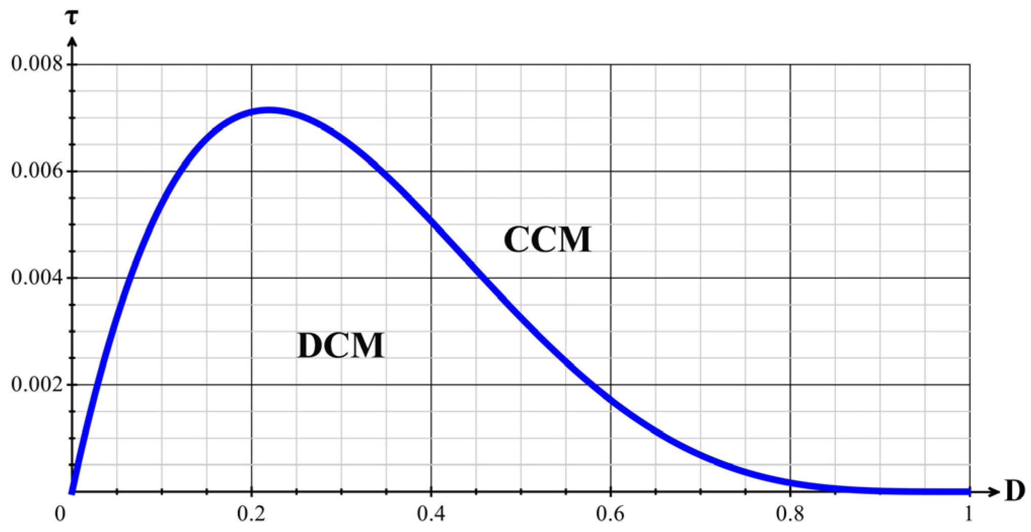
τ B C M , L 1 = τ B L = D 2 1 D 4 6.4 1 1 D 2
Figure 6 shows the inductor current (τBL) constant versus the duty cycle (D).

4. Design Considerations and Components’ Selection

The design considerations needed to obtain the values for different components in the proposed converter are presented in this section.
The useful equations and guidelines will be explained in detail; the component values are shown in Table 1.

4.1. The Design of Inductors L1, L2 and L3

Equations (60)–(62) express the inductance of L1, L2, and L3, respectively. In (60), ∆IL1 expresses the peak-to-peak changes in inductor current IL1. Furthermore, fS shows the switching frequency of the circuit in these equations. It should be mentioned that inductance values of L1, L2, and L3 are obtained when the switch is turned on:
L 1 2 D V S Δ I L 1 × f s ( 1 D )
In (61), ∆IL2 expresses the peak-to-peak changes of inductor current IL2:
L 2 D V S Δ I L 2 × f s ( 1 D )
In (62), ∆IL3 expresses the peak-to-peak changes of inductor current IL3:
L 3 D V S Δ I L 3 × f s
Depending on the converter operation in CCM, the number of inductor current changes should be designed so that the converter always operates in CCM, and does not enter DCM. For this purpose, the number of current changes through input inductors L1, L2, and L3 is equal to 20%, 10%, and 5% of the nominal average current that flows through them, respectively.

4.2. The Design of Capacitors C1, C2, C3, C4 and the Output Capacitor CO

According to the converter operation, the capacitances of C1 and C2 are equal. Their values are obtained from Equation (63) when the switch is turned off.
C 1 = C 2 V O ( 1 D ) Δ V C 1 × f s × R
It should be noted that the voltage variations (ΔVC1 and ΔVC2) are considered 5% of the nominal average voltage across each capacitor. Furthermore, the capacitances of C3 and C4 are equal. According to the output cell, their values are calculated from Equation (64) when the switch is turned on. Besides, ∆V is the voltage change across the capacitors in the following equations:
C 3 = C 4 P O × D Δ V C 3 × f s × V O
Similar to the calculation of capacitors C1 and C2, the number of voltage changes (ΔVC3 and ΔVC4) is considered 5% of the nominal average voltage across each capacitor. The capacitance of output capacitor CO is computed as follows.
C o V O × D Δ V O × f s × R

4.3. The Current and Voltage Stresses of Switch S

To select the appropriate switches and diodes in the proposed converter, the output power is first considered the main factor in selecting the type of active components. Then, the voltage and current stresses are calculated, and the appropriate diodes and switches are selected. According to the operation modes, the voltage and current stresses of the switch are obtained as follows.
V S W = V O 2
I S W = P O V S I O ( max )

4.4. The Current and Voltage Stresses of Diodes D1, D2, D3, D4, D5, D6, and D7

The voltage and current stresses of diode D1 are calculated as follows:
V D 1 = V O 2 4 V S
I D 1 = P O V S ( I L 1 Δ I L 1 2 )
The voltage and current stresses of diode D2 are considered as follows:
V D 2 = 4 V S
I D 2 = P O V S ( I L 2 Δ I L 2 2 )
The voltage and current stresses of diode D3 are measured as follows:
V D 3 = V O 2 + 2 V S
I D 3 = P O V S ( I L 1 Δ I L 1 2 ) ( I L 2 Δ I L 2 2 )
The voltage and current stresses of diode D4 are computed as follows:
V D 4 = 2 V S
I D 4 = I L 3 + Δ I L 3 2 I O
The voltage and current stresses of diode D5 are calculated as follows:
V D 5 = V O 2
I D 5 = I O 2
The voltage and current stresses of diode D6 are designed as follows:
V D 6 = V O 2
I D 6 = I O
The voltage and current stresses of diode D7 are obtained as follows:
V D 7 = V O 2
I D 7 = I O 2

5. Control of the Converter

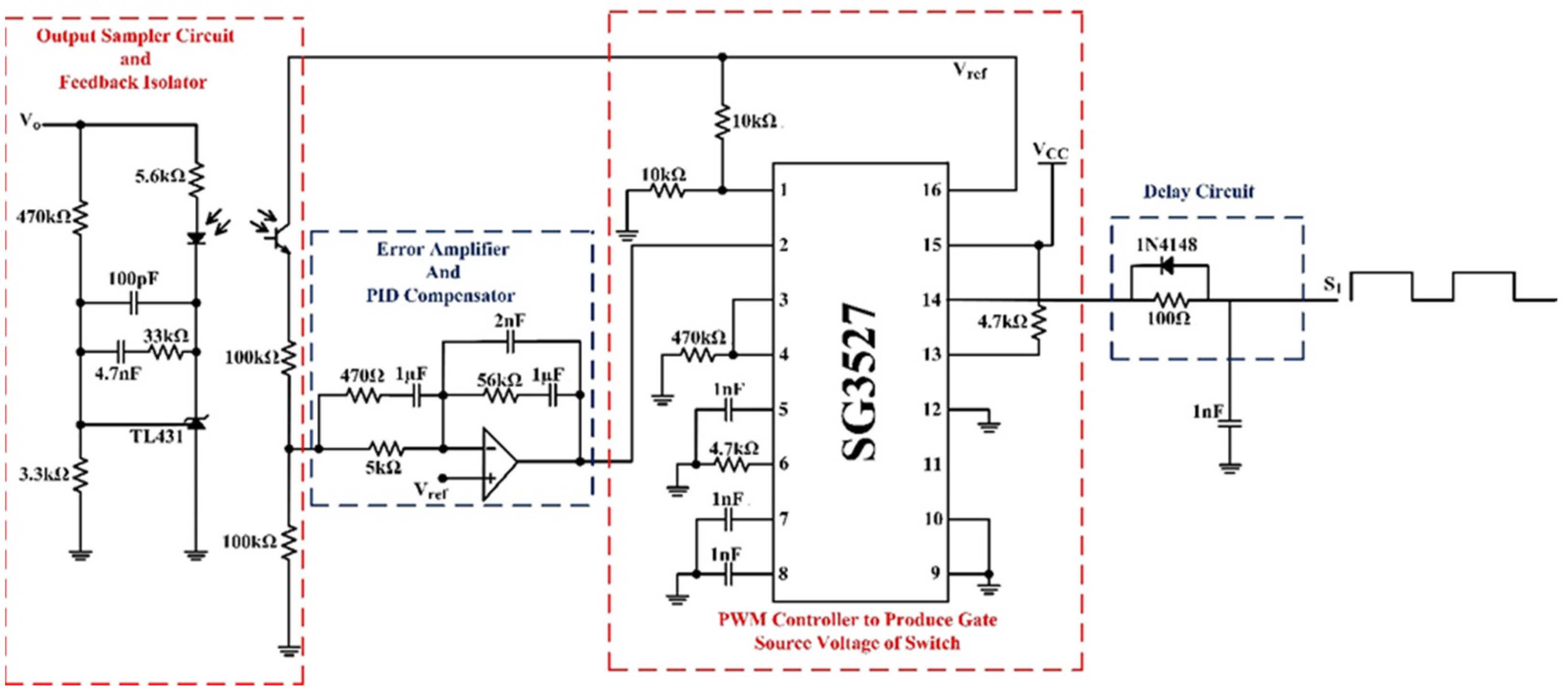
The experimental control circuit includes four parts, as shown in Figure 7. An output sampler circuit and feedback isolator create the first part, made up of an optocoupler and TL431. A PID compensator and an error amplifier make up the second part. A PWM controller (SG3527 IC) is used for the switch in the third part. To adjust the produced signal in the prior stage, a pulse delay circuit is used in the fourth part. A control circuit is used to stabilize the output voltage when the load changes. This phenomenon is shown in Figure 8.

6. Experimental Results

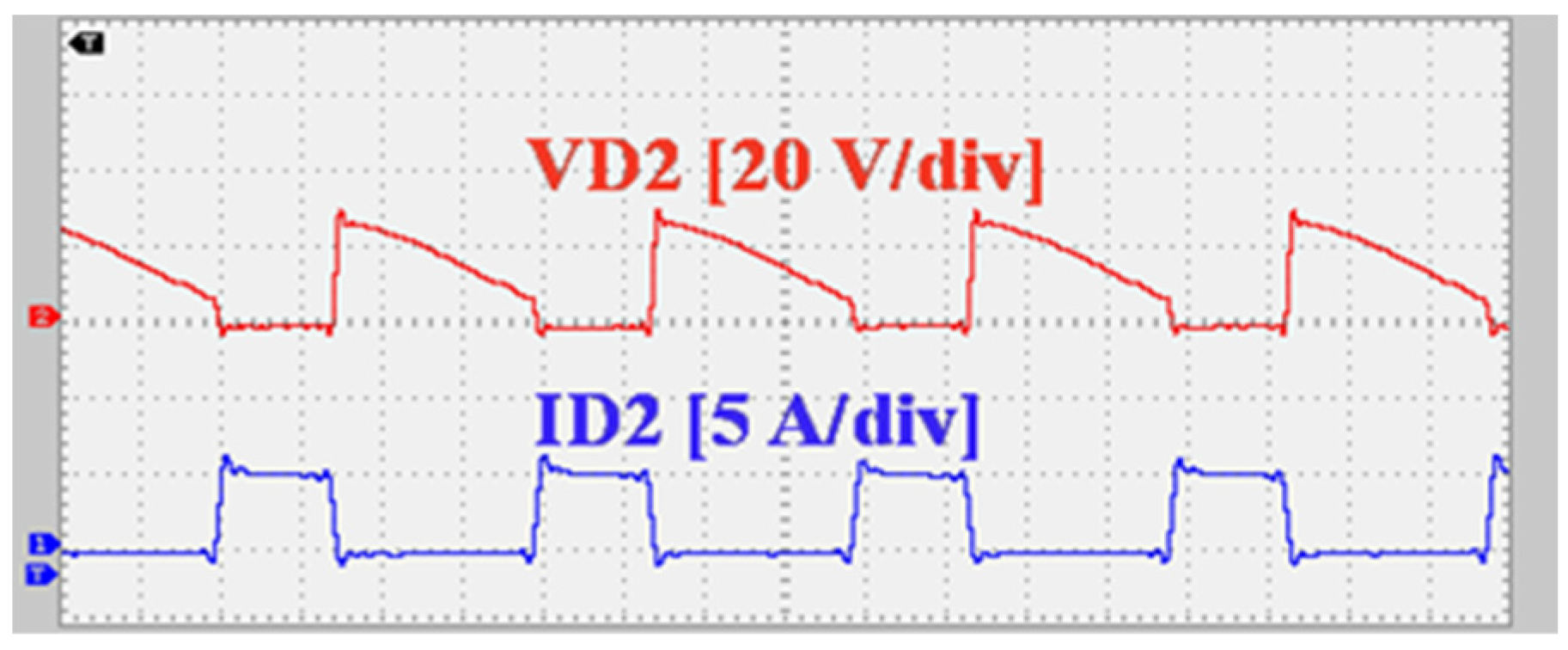
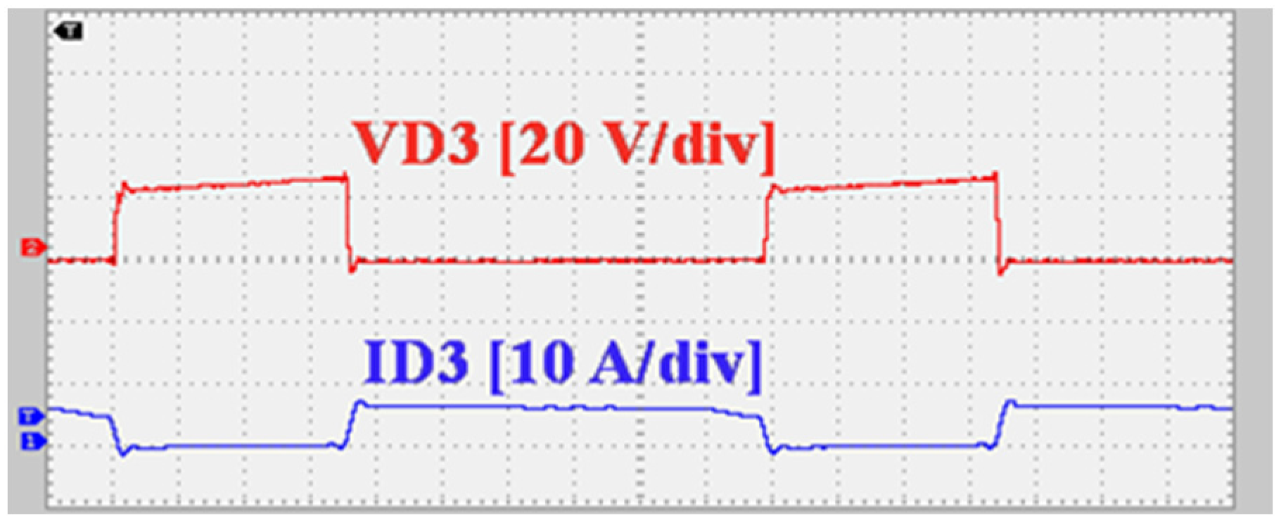
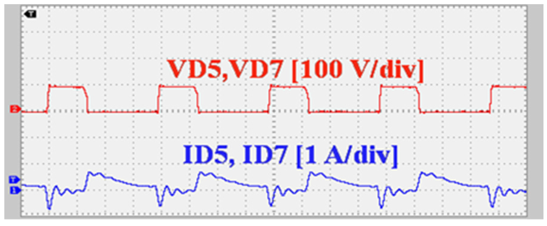
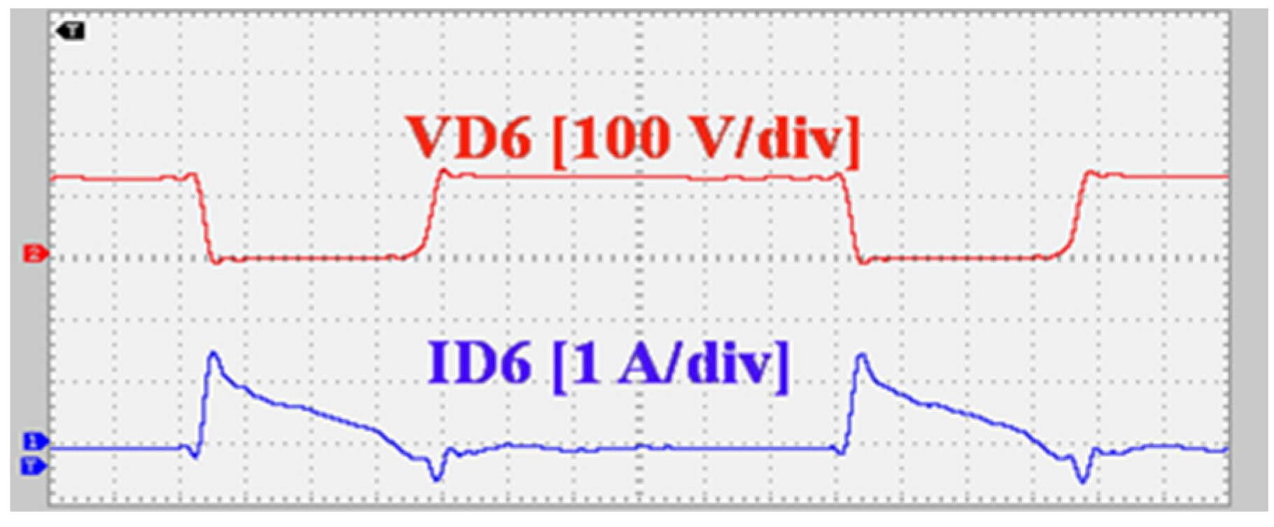
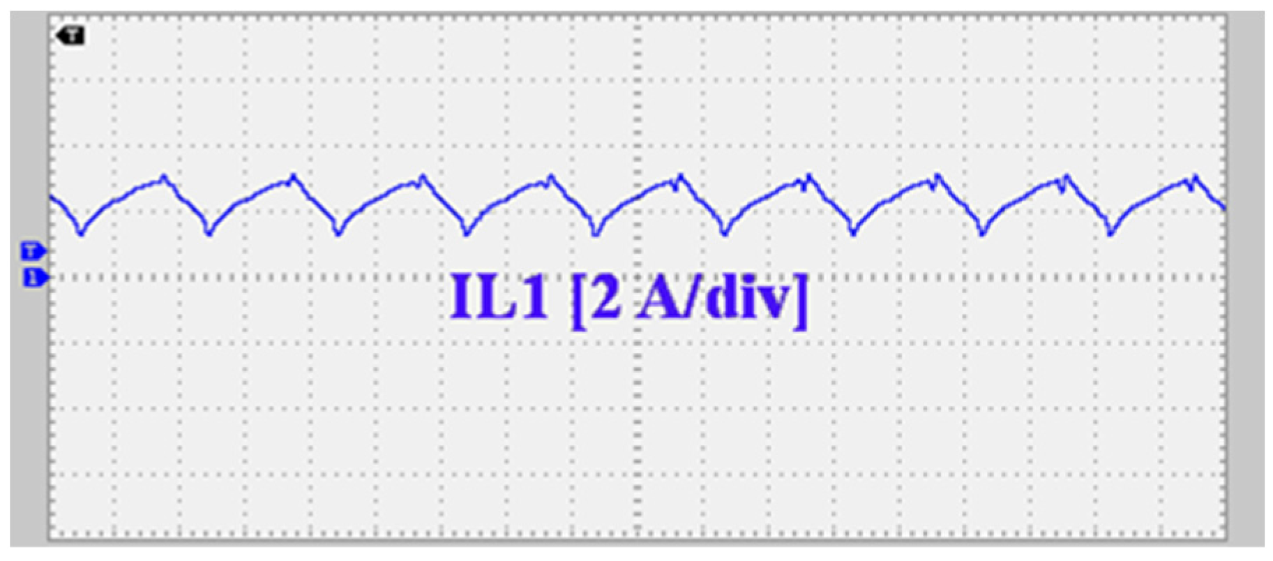
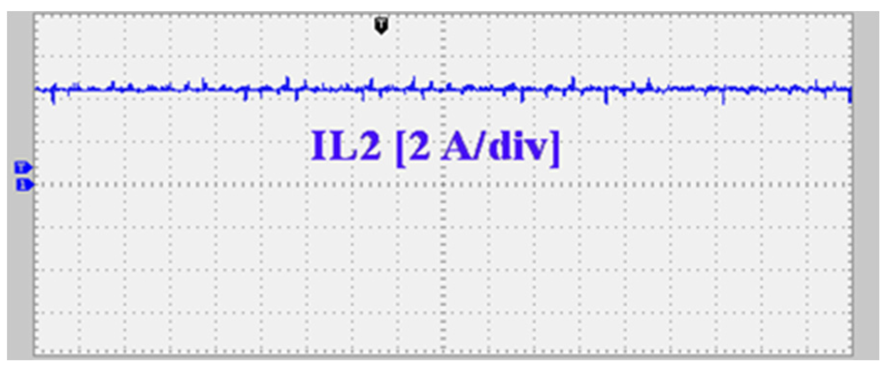
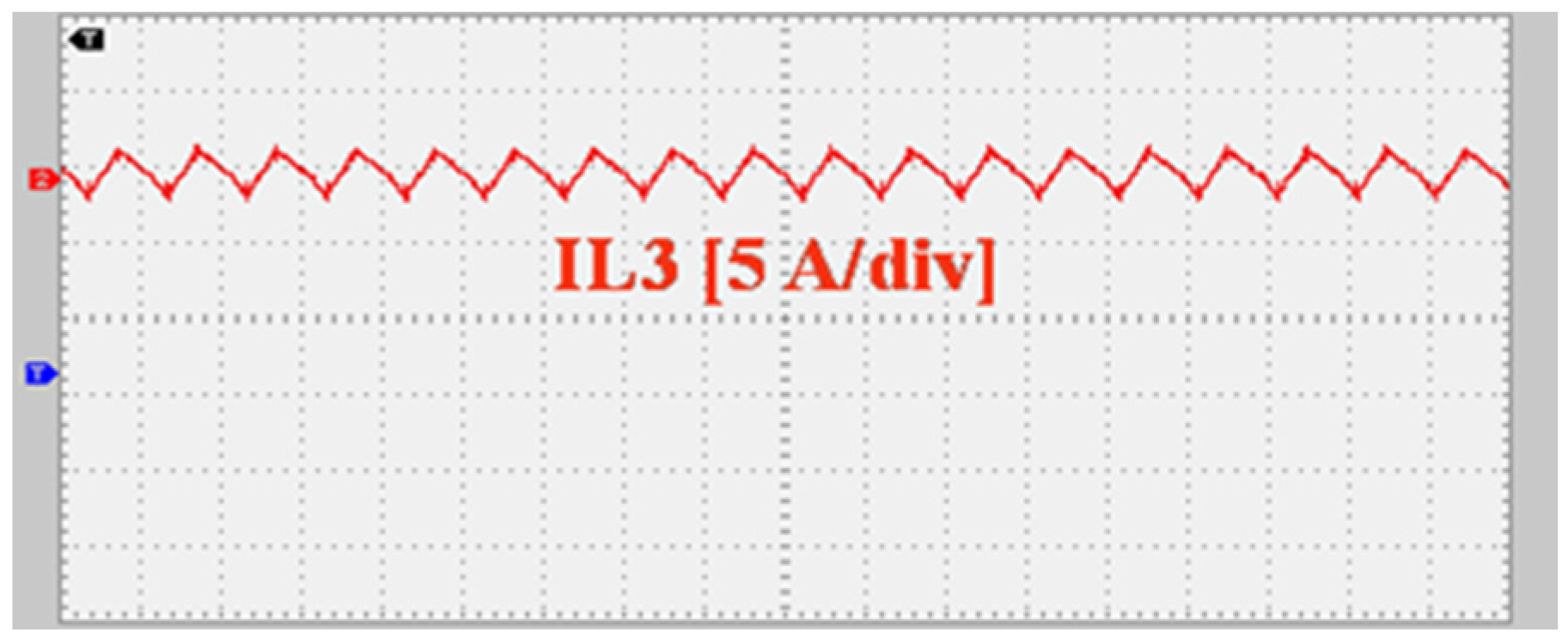
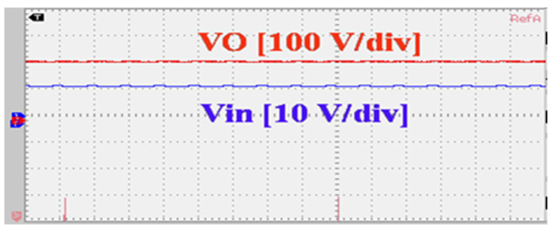
A 110 W prototype of the proposed switched-inductor switched-capacitor DC-DC converter with a single switch was implemented. The switching frequency was 100 kHz and the voltage gain was 21.6. These value were obtained without using any transformer in the proposed converter. Based on the current and voltage stresses mentioned in the former section, IRFP260 was selected for the switch. Furthermore, STPS16150CT was selected for all diodes in the converter. The voltage and current waveforms for the switch are shown in Figure 9. The voltage and current waveforms of diodes D1, D2, D3, D4, D5, D6, and D7 are illustrated in Figure 10, Figure 11, Figure 12, Figure 13, Figure 14 and Figure 15, respectively. Furthermore, inductor currents IL1, IL2, and IL3 are presented in Figure 16, Figure 17 and Figure 18, correspondingly. Moreover, input and output voltages are shown in Figure 19.
According to Figure 9, switch S is turned on at t0, and the sum of IL1, IL2, IL3, and ID6 flow through it. Since diodes D5 and D7 are forward-biased when the switch is off, the inductor currents do not create voltage spikes across the switch.
Based on the converter operation and Figure 10, diode D1 is switched on when the switch conducts, and it tolerates the sum of IL2 and IL3. Diode D1 is switched off when the switch is turned off. In this condition, the power transfers from the input source and inductor L1 through diode D2.
According to the operation modes, the performance of the even-numbered diodes is opposite to that of the odd-numbered diodes. Based on Figure 11, diode D2 is switched on when the switch is turned off and the input current flows through it. When the switch is on, diode D2 is reverse-biased, and the path is created by diode D1 for transferring the energy to inductor L1.
The operation of diode D3 is similar to diode D1. When the switch is turned on, IL3 flows through the diode.
The operation of diode D4 is similar to diode D2. When the switch is turned off, IL3 flows through the diode.
Diodes D5 and D7 have similar performance. Since they are located on two parallel and symmetric paths, D5 and D7 have similar current and voltage stresses. These diodes create the path to transfer the power from all the energy storage elements and the input source to the load.
The operation of diode D6 is opposite to the operation of diodes D5 and D7, and creates the path to charge the switched capacitors C3 and C4.
The current ripples of inductors L1, L2, and L3 are calculated and analyzed in theoretical waveforms (Figure 4a). As shown in Figure 16, Figure 17 and Figure 18, the current ripple of inductor L1 is higher than the current ripple of inductors L2 and L3.

7. Performance Comparison

A comparison between the proposed converter and different topologies in terms of voltage gain, switching frequency, and number of components is presented in Table 2. Moreover, the power losses of the proposed converter are presented in Table 3. The comparison shows the advantages of the converter. A comparison of the voltage gain per duty cycle of the proposed converter with other high-step-up converters is represented in Figure 20.
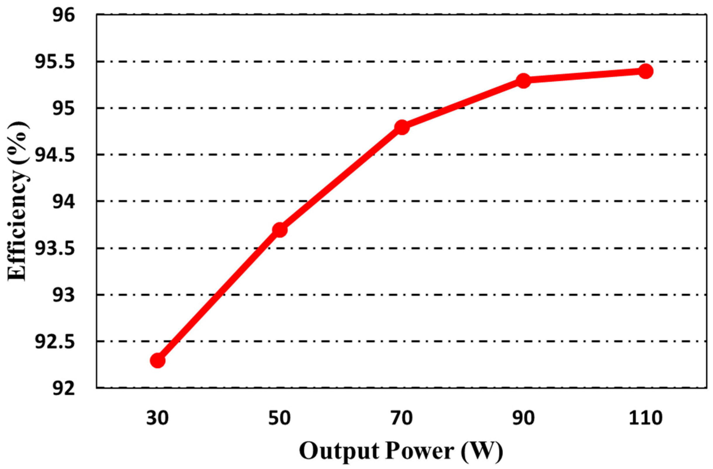
It is obvious that the total switch count (TSC) is an important factor in designing a converter. In fact, a lower TSC leads to a simpler control circuit. Figure 21 supports that the proposed converter achieves a high voltage gain with a lower TSC. The efficiency curve of the proposed converter under different load conditions is shown in Figure 22. It is clear that the total efficiency of the converter at nominal power is 95.4%. Finally, the power loss distribution at 110 W for the proposed converters is shown in Figure 23.

8. Conclusions

This paper successfully introduces and details a novel high-step-up, non-isolated switched-inductor switched-capacitor DC-DC converter, demonstrating its superior performance in achieving high voltage gain. The simplicity of its design, characterized by a single-switch structure and PWM control, is a game-changer in the realm of DC-DC converters. The proposed converter outperforms other similar structures with respect to several critical factors, including the number of active and passive elements, voltage gain, and switching frequency. As evidenced by the constructed prototype, the converter operates with an input voltage of 12 V, and delivers an output voltage of 260 V, with a switching frequency of 100 kHz and a nominal power of 110 W. Remarkably, this high voltage gain (21.6) is accomplished without the use of any transformer or coupled inductors, setting this non-isolated converter apart from its peers. The findings of this study confidently affirm the proposed converter’s potential for significant applications in the field of renewable energy systems.

Author Contributions

Conceptualization, M.S., A.M. and M.R.; Methodology, M.S., A.M. and M.R.; Software, M.S.; Validation, M.S.; Formal analysis, M.S. and A.M.; Writing—original draft, M.S., A.M., M.R. and F.K.; Writing—review & editing, S.A.G.; Supervision, A.M. and S.A.G.; Project administration, F.K.; Funding acquisition, S.A.G. All authors have read and agreed to the published version of the manuscript.

Funding

This research received no external funding.

Conflicts of Interest

The authors declare no conflict of interest.

References

  1. Revanyvardom, M.; Mirzaei, A. High gain configuration of modified ZVT SEPIC-Boost DC-DC converter with coupled inductors for photovoltaic applications. Sol. Energy 2020, 208, 357–367. [Google Scholar] [CrossRef]
  2. Taghavi, S.-S.; Rezvanyvardom, M.; Mirzaei, A.; Gorji, S.A. High Step-Up Three-Level Soft Switching DC-DC Converter for Photovoltaic Generation Systems. Energies 2023, 16, 41. [Google Scholar] [CrossRef]
  3. Salvador, M.A.; Lazzarin, T.B.; Coelho, R.F. High step-up DC–DC converter with active switched-inductor and passive switched-capacitor networks. IEEE Trans. Ind. Electron. 2017, 65, 5644–5654. [Google Scholar] [CrossRef]
  4. Ramanathan, G.G.; Urasaki, N. Non-Isolated Interleaved Hybrid Boost Converter for Renewable Energy Applications. Energies 2022, 15, 610. [Google Scholar] [CrossRef]
  5. Liu, H.-C.; Li, F. Novel high step-up DC–DC converter with an active coupled-inductor network for a sustainable energy system. IEEE Trans. Power Electron. 2015, 30, 6476–6482. [Google Scholar] [CrossRef]
  6. Gorji, S.A. Reconfigurable Quadratic Converters for Electrolyzers Utilized in DC Microgrids. IEEE Access 2022, 10, 109677–109687. [Google Scholar] [CrossRef]
  7. Gholizadeh, H.; Sharifi Shahrivar, R.; Hashemi, M.R.; Afjei, E.; Gorji, S.A. Design and Implementation a Single-Switch Step-Up DC-DC Converter Based on Cascaded Boost and Luo Converters. Energies 2021, 14, 3584. [Google Scholar] [CrossRef]
  8. Gautam, V.; Sensarma, P. Design of Ćuk-Derived Transformer-less Common-Grounded PV Micro inverter in CCM. IEEE Trans. Ind. Electron. 2017, 64, 6245–6254. [Google Scholar] [CrossRef]
  9. Rezvanyvardom, M.; Mirzaei, A.; Heydari, S. Fully Soft-Switching Non-isolated Quasi-Z-Source DC–DC Converter with High-Voltage Gain. IEEE J. Emerg. Sel. Top. Power Electron. 2021, 9, 1854–1862. [Google Scholar] [CrossRef]
  10. Afzal, R.; Tang, Y.; Tong, H.; Guo, Y. A High Step-up Integrated Coupled Inductor-Capacitor DC-DC Converter. IEEE Access 2021, 9, 11080–11090. [Google Scholar] [CrossRef]
  11. Akhlaghi, B.; Farzanehfard, H. Soft Switching Interleaved High Step-Up Converter with Multifunction Coupled Inductors. IEEE J. Emerg. Select. Top. Ind. Electr. 2021, 2, 13–20. [Google Scholar] [CrossRef]
  12. Kothapalli, K.R.; Ramteke, M.R.; Suryawanshi, H.M.; Reddi, N.K.; Kalahasthi, R.B. A Coupled Inductor Based High Step-Up Converter for DC Microgrid Applications. IEEE Trans. Ind. Electron. 2021, 68, 4927–4940. [Google Scholar] [CrossRef]
  13. Zhu, X.; Zhang, B.; Li, Z.; Li, H.; Ran, L. Extended switched-boost DC-DC converters adopting switched-capacitor/switched-inductor cells for high step-up conversion. IEEE J. Emerg. Sel. Top. Power Electron. 2016, 5, 1020–1030. [Google Scholar] [CrossRef]
  14. Tang, Y.; Wang, T.; Fu, D. Multi cell switched-inductor/switched capacitor combined active-network converters. IEEE Trans. Power Electron. 2014, 30, 2063–2072. [Google Scholar] [CrossRef]
  15. Chen, M.; Li, K.; Hu, J.; Ioinovici, A. Generation of a Family of Very High DC Gain Power Electronics Circuits Based on Switched-Capacitor-Inductor Cells Starting from a Simple Graph. IEEE Trans. Circuits Syst. I Regul. Pap. 2016, 63, 2381–2392. [Google Scholar] [CrossRef]
  16. Axelrod, B.; Berkovich, Y.; Ioinovici, A. Switched-Capacitor/Switched-Inductor Structures for Getting Transformerless Hybrid DC–DC PWM Converters. IEEE Trans. Circuits Syst. I Regul. Pap. 2008, 55, 687–696. [Google Scholar] [CrossRef]
  17. Tang, Y.; Fu, D.; Wang, T.; Xu, Z. Hybrid Switched-Inductor Converters for High Step-Up Conversion. IEEE Trans. Ind. Electron. 2015, 62, 1480–1490. [Google Scholar] [CrossRef]
  18. Kumar, G.G.; Sundaramoorthy, K.; Karthikeyan, V.; Babaei, E. Switched Capacitor–Inductor Network Based Ultra-Gain DC–DC Converter Using Single Switch. IEEE Trans. Ind. Electron. 2020, 67, 10274–10283. [Google Scholar] [CrossRef]
  19. Salvador, M.A.; de Andrade, J.M.; Lazzarin, T.B.; Coelho, R.F. Non-isolated High-Step-Up DC–DC Converter Derived from Switched-Inductors and Switched-Capacitors. IEEE Trans. Ind. Electron. 2020, 67, 8506–8516. [Google Scholar] [CrossRef]
  20. Sudhakar, R.S.; Gajjala, S.; Praveen, M.S.; Kumar, I.K. High Efficiency DC-DC Boost Converter with Stacked Capacitors for Renewable Energy Applications. In Proceedings of the 2020 4th International Conference on Electronics, Communication and Aerospace Technology (ICECA), Coimbatore, India, 5–7 November 2020; pp. 378–384. [Google Scholar]
  21. Alharbi, B.M.; Alhomim, M.A.; McCann, R.A. A High Voltage Ratio Three-stage Cascaded Interleaved Boost Converters for PV Application. In Proceedings of the 2020 IEEE Power and Energy Conference at Illinois (PECI), Champaign, IL, USA, 27–28 February 2020; pp. 1–5. [Google Scholar]
  22. Zhao, Q.; Lee, F.C. High-efficiency, high step-up DC-DC converters. IEEE Trans. Power Electron. 2003, 18, 65–73. [Google Scholar] [CrossRef] [Green Version]
  23. Schmitz, L.; Martins, D.C.; Coelho, R.F. Generalized High Step-Up DC-DC Boost-Based Converter with Gain Cell. IEEE Trans. Circuits Syst. I Regul. Pap. 2017, 64, 480–493. [Google Scholar] [CrossRef]
  24. Abutbul, O.; Gherlitz, A.; Berkovich, Y.; Ioinovici, A. Step-up switching-mode converter with high voltage gain using a switchedcapacitor circuit. IEEE Trans. Circuits Syst. I Fundam. Theory Appl. 2003, 50, 1098–1102. [Google Scholar] [CrossRef]
  25. Chen, J.; Ding, K.; Zhong, Y.; Deng, F.; Abulanwar, S. A double input-parallel-output-series hybrid switched-capacitor boost converter. Chin. J. Electr. Eng. 2020, 6, 15–27. [Google Scholar] [CrossRef]
  26. Sadaf, S.; Bhaskar, M.S.; Meraj, M.; Iqbal, A.; Al-Emadi, N. A Novel Modified Switched Inductor Boost Converter with Reduced Switch Voltage Stress. IEEE Trans. Ind. Electron. 2021, 68, 1275–1289. [Google Scholar] [CrossRef]
  27. Wu, G.; Ruan, X.; Ye, Z. Non-isolated High Step-Up DC–DC Converters Adopting Switched-Capacitor Cell. IEEE Trans. Ind. Electron. 2015, 62, 383–393. [Google Scholar] [CrossRef]
  28. Wang, P.; Zhou, L.; Zhang, Y.; Li, J.; Sumner, M. Input-Parallel Output-Series DC-DC Boost Converter with a Wide Input Voltage Range, For Fuel Cell Vehicles. IEEE Trans. Veh. Technol. 2017, 66, 7771–7781. [Google Scholar] [CrossRef]
  29. Zhang, Y.; Zhou, L.; Sumner, M.; Wang, P. Single-Switch, Wide Voltage-Gain Range, Boost DC–DC Converter for Fuel Cell Vehicles. IEEE Trans. Veh. Technol. 2018, 67, 134–145. [Google Scholar] [CrossRef]
  30. Lakshmi, M.; Hemamalini, S. Nonisolated High Gain DC–DC Converter for DC Microgrids. IEEE Trans. Ind. Electron. 2018, 65, 1205–1212. [Google Scholar] [CrossRef]
  31. Wu, B.; Li, S.; Liu, Y.; Smedley, K.M. A New Hybrid Boosting Converter for Renewable Energy Applications. IEEE Trans. Power Electron. 2016, 31, 1203–1215. [Google Scholar] [CrossRef]
  32. Luo, F.L.; Ye, H. Positive output cascade boost converters. IEE Proc. Electr. Power Appl. 2004, 151, 590–606. [Google Scholar] [CrossRef]
  33. Nouri, T.; Hosseini, S.H.; Babaei, E.; Ebrahimi, J. Generalised transformerless ultra step-up DC–DC converter with reduced voltage stress on semiconductors. IET Power Electron. 2014, 7, 2791–2805. [Google Scholar] [CrossRef]
  34. Gu, Y.; Chen, Y.; Zhang, B.; Qiu, D.; Xie, F. High Step-Up DC–DC Converter with Active Switched LC-Network for Photovoltaic Systems. IEEE Trans. Energy Convers. 2019, 34, 321–329. [Google Scholar]
  35. Li, K.; Hu, Y.; Ioinovici, A. Generation of the Large DC Gain Step-Up Non-isolated Converters in Conjunction with Renewable Energy Sources Starting from a Proposed Geometric Structure. IEEE Trans. Power Electron. 2017, 32, 5323–5340. [Google Scholar] [CrossRef]
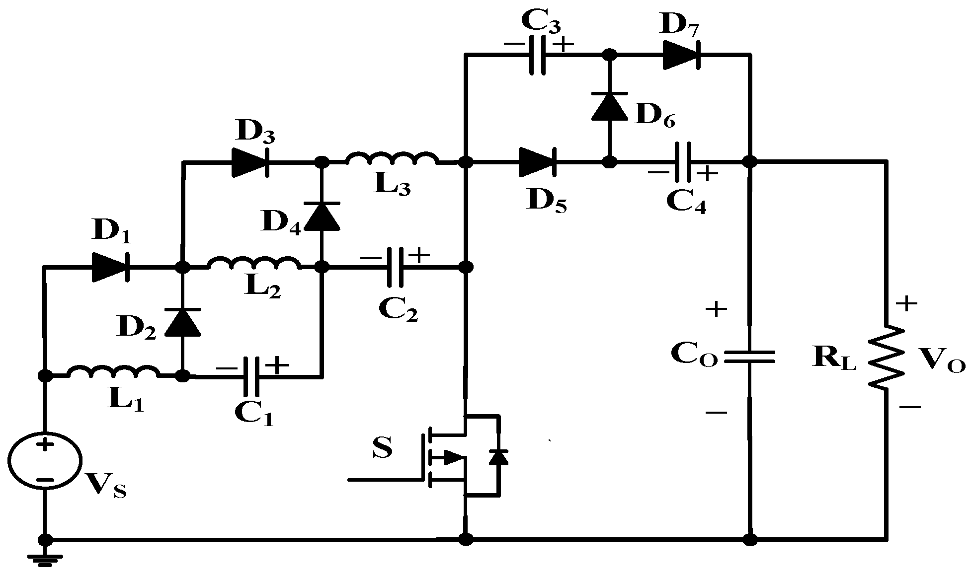
Figure 1. The proposed high-step-up non-isolated DC-DC converter.
Energies 16 05524 g001
Figure 2. The proposed switch-inductor switched-capacitor cell.
Energies 16 05524 g002
Figure 3. The switched-capacitor cell.
Energies 16 05524 g003
Figure 4. Theoretical waveforms of the proposed converter, where blue is voltage and red is current: (a) voltage and currents across switch inductors and first diode (b) voltage and current across capacitors and other diodes.
Energies 16 05524 g004
Figure 5. Equivalent circuit for the proposed converter: (a) mode 1, (b) mode 2, and (c) mode 3 in DCM operation.
Energies 16 05524 g005
Figure 6. Boundaries of the proposed converter.
Energies 16 05524 g006
Figure 7. Characteristics of the control circuit.
Energies 16 05524 g007
Figure 8. The influence of load variations on the output voltage. (a) Changing 25 to 100% of the rated load, and (b) changing 50 to 100% of the rated load.
Energies 16 05524 g008
Figure 9. Voltage and current waveforms of switch S.
Energies 16 05524 g009
Figure 10. Voltage and current waveforms of diode D1.
Energies 16 05524 g010
Figure 11. Voltage and current waveforms of diode D2.
Energies 16 05524 g011
Figure 12. Voltage and current waveforms of diode D3.
Energies 16 05524 g012
Figure 13. Voltage and current waveforms of diode D4.
Energies 16 05524 g013
Figure 14. Voltage and current waveforms of diodes D5 and D7.
Energies 16 05524 g014
Figure 15. Voltage and current waveforms of diode D6.
Energies 16 05524 g015
Figure 16. Inductor current waveform IL1.
Energies 16 05524 g016
Figure 17. Inductor current waveform IL2.
Energies 16 05524 g017
Figure 18. Inductor current waveform IL3.
Energies 16 05524 g018
Figure 19. Output voltage and input voltage waveforms.
Energies 16 05524 g019
Figure 20. Comparison of voltage gain in the proposed converter versus other high-step-up converters [3,14,15,16,18].
Energies 16 05524 g020
Figure 21. Comparison of the voltage gain to total switch count (TSC) ratio at different duty cycles [3,14,15,16,18].
Energies 16 05524 g021
Figure 22. Efficiency under different load conditions.
Energies 16 05524 g022
Figure 23. Power loss distribution at 110 W.
Energies 16 05524 g023
Table 1. Component values.
ParameterValue
Input voltage12 V
Output voltage260 V
Switching frequency100 kHz
Output power110 W
Capacitors C1, C2, C3, C410 µF
Output capacitor CO20 µF
Inductor L1650 µH
Inductor L2350 µH
Inductor L3150 µH
Table 2. Comparison between the proposed converter and similar structures.
Ref.Voltage
Gain
Normalized
Voltage Stress
EfficiencyRated PowerSwitching
Frequency
No. of Components
SwitchDiodeSDLC
[3](3D + 1)/(1 − D)1/(1 − D)2/(1 − D)94.45%200 W50 kHz2233
[13]2(1 − D)/(1 − 3D)2D/(1 − 3D)2D/(1 − 3D)91%90 W30 kHz2723
[14](5D + 1)/(1 − D)(G + 1)/4(G − 1)/891.5%200 W100 kHz2943
[15]4/(1 − D)G/2G/290.73%100 W200 kHz2615
[16](1 + D)/(1 − D)GG-50 W40 kHz1421
[17](3D + 1)/(1 − D)(G + 1)/2G + 194.5%200 W50 kHz2741
[18](2 − D)/(1 − D)21/(1 − D)2D/(1 − D)288%500 W50 kHz1423
[19](3D + 1)/(1 − D)G/(3 + D)2G/(3 + D)94.3%200 W50 kHz2323
Proposed4/(1 − D)2G/2(G/2) + 295.4%110 W100 kHz1735
Table 3. Power losses in the proposed converter.
Type of LossFormulaProposed Converter (W)
Switching loss in the main switch (S) 1 2 . V i n + V C 1 . I O . t o n + t o f f + ( V i n + V C 1 ) . I O + I r r . t r r . F S W 0.37
Parasitic capacitance loss in the main switch (S) 1 2 . C o u t . V i n + V C 1 2 . F S W 0.047
Conduction loss in the main switch (S) R d s . F S W . 0 T I S 2   d t 0.63
Conduction loss in the input cells diodes (D1, D2, D3, and D4) I a v e . V F 0.68
Conduction loss in the output cell diodes (D5, D6, and D7) I a v e . V F 0.64
Loss of inductors P L o s s = P C o r e + P C o p p e r
P C o r e = K 1 . F S W . B y . V e
P C o p p e r = P d c r + P a c r =
( I r m s 1 2 × D C R ) + I r m s 2 2 × A C R
2.55
Loss of capacitors P d = E S R × I a v e 2 0.58
Total losses-5.5 W
Disclaimer/Publisher’s Note: The statements, opinions and data contained in all publications are solely those of the individual author(s) and contributor(s) and not of MDPI and/or the editor(s). MDPI and/or the editor(s) disclaim responsibility for any injury to people or property resulting from any ideas, methods, instructions or products referred to in the content.