Article

A Family of Zero-Voltage-Transition Magnetic Coupling Bidirectional DC/DC Converters †

College of Electrical Engineering, Zhejiang University, Hangzhou 310007, China
*
Author to whom correspondence should be addressed.
This paper is an extended version of our paper published in 2022 12th International Conference on Power, Energy and Electrical Engineering (CPEEE), Shiga, Japan, 25–27 February 2022; pp. 180–184.
Energies 2023, 16(12), 4760; https://doi.org/10.3390/en16124760
Submission received: 10 April 2023 / Revised: 7 June 2023 / Accepted: 12 June 2023 / Published: 16 June 2023
(This article belongs to the Special Issue Advanced DC-DC Power Converters and Switching Converters II)

Abstract

:
In this paper, a family of zero-voltage-transition (ZVT) magnetic coupling bidirectional DC/DC converters (BDCs) is proposed. The coupling inductor has two functions: to serve as a filter; and to provide the auxiliary current. In addition, the phase-shifting control method is used to reduce the conduction loss of the auxiliary circuit. The auxiliary switches are all working under zero-current-switching (ZCS) conditions; thus, all the switches have no switching loss. Furthermore, compared with the traditional ZVT implementation method based on the coupled inductor, this topology avoids the input source current notch and has a smaller ripple. Finally, a prototype of 800 W BDC is built to verify the feasibility of the proposed topology.

1. Introduction

With the continuous growth of systems with energy storage devices, research on bidirectional DC–DC converters has been greatly promoted. Bidirectional DC–DC converters are widely used in photovoltaic and energy storage systems [1,2], electric/hybrid vehicles [3,4], uninterrupted power supply systems [5], fuel cell power systems [6,7], etc. In these applications, converters are required to have low current ripple requirements at the energy storage port. If electrical isolation is not required between the high-voltage port and low-voltage port, the BDC topology is usually chosen due to its low cost and simple structure. For BDC, switching loss is the main reason for limiting frequency increases. Therefore, in order to achieve a high-efficiency and high-frequency power conversion of BDC, it is necessary to introduce soft-switching technology.
One effective method to achieve the purpose of soft-switching is to make the BDC work in near-critical conduction modes [8,9,10]. However, the input current has a larger ripple, which leads to a high conduction loss and easy core saturation.
Quasi-resonant technology realizes the zero-voltage-switching (ZVS) of the main switch by using LC resonance to generate zero voltage when the main switch is turned on [11,12]. However, a large circulating current exists in the circuit, which leads to an increase in conduction loss. In addition, the switching frequency changes in a wide range when the load changes greatly, which will make the design of passive devices more difficult.
Active clamp ZVS technology also needs to add a resonant inductor in the main circuit to realize the ZVS of the main switch [13,14]. The circulating current of the auxiliary circuit is large, which increases the conduction loss. Moreover, the main switch has high voltage stress.
As the auxiliary circuit is removed from the main circuit and the auxiliary switch operates only during the period before and after the main switch is turned on, the conduction loss in the ZVT converter is reduced, while the voltage stress of the main switch is lower than that of the quasi-resonant converter and active clamp converter [15,16,17,18]. These ZVT converters all need additional inductors as resonant inductors, which are disadvantageous to the improvement of power density because of the large volume and weight of magnetic components. Several soft-switching technologies based on coupled inductors have been proposed in [19,20,21,22,23,24,25,26,27,28].
In [19], a coupled winding is added to the same core of the main inductor to realize the soft switching of the main switch. In the ZVT BDC proposed in [20], a coupled inductor and two unidirectional auxiliary switches are used in the auxiliary circuit. A ZVT BDC is described in [21], while the auxiliary circuit consists of a coupled inductor and two auxiliary switches. A family of ZVS Buck, ZVS Boost, and ZVS BDC topologies is presented in [22], and the auxiliary circuit consists of a coupled inductor and a diode. In [23], a family of ZVS magnetic coupling BDC topologies is proposed. In those BDCs, the additional circuits contain two auxiliary switches. Two auxiliary voltage sources composed of passive components are used in the auxiliary circuit of the ZVS BDC in [24]. A ZVT BDC is proposed in [25], in which the auxiliary circuit consists of a coupled inductor, two unidirectional switches, and an auxiliary capacitor. In [26], a ZVT BDC is studied, in which all the switches implement ZVS or ZCS conditions. In [27], several ZVS DC–DC converters based on coupled inductors are proposed by changing the connection position of the coupling branch. A ZVS magnetic coupling BDC with no current notch at the low-voltage port is proposed in [28]. In [29], a ZVT PWM BDC based on coupled inductors is proposed. This topology needs two cores, increasing the complexity of the system. An overview of soft-switching technologies for BDC is given in [30].
As shown in Figure 1, there is an input current notch in the ZVS BDCs proposed in [20,21,23,24,26], which would hurt the life of storage equipment. In this paper, a family of ZVT magnetic coupling BDCs is proposed. The coupling inductor not only serves as a filter but also provides the auxiliary current. Compared with the traditional ZVS implementation method, this topology avoids the input source current notch and has a smaller ripple.
In Section 2, the topologies and operation process are demonstrated. In Section 3, the ZVT conditions of the main switches, the loss analysis, and the comparison between the proposed ZVT BDCs and the existing ZVT BDCs are given in detail. Moreover, the current frequency spectrum of the low-voltage port comparison between the proposed ZVT BDC and the traditional ZVT BDC is provided. In Section 4, the experimental results verify the validity of the topology. Finally, the conclusions are summarized.

2. Operation Process Analysis

2.1. Proposed ZVT BDCs

The ZVT magnetic coupling BDCs are shown in Figure 2. S1 and S2 are the switches of the main power circuit. SSS1 and SSS2 are the switches of the auxiliary circuit. CS1, CS2, and Ca are the three auxiliary capacitors. The coupled inductor is equivalent to an ideal transformer T, Lm (the excitation inductor), and Lr (the leakage inductor). C1 and C2 are filter capacitors of Port 1 and Port 2. The difference between Topology 1 (as shown in Figure 2a) and Topology 2 (as shown in Figure 2b) is that the auxiliary circuit of Topology 1 is connected between Port 2 and the ground, and the auxiliary circuit of Topology 2 is connected between Port 1 and Port 2.

2.2. Operation Analysis of the Proposed ZVS BDCs

2.2.1. Operation Analysis of Topology 1

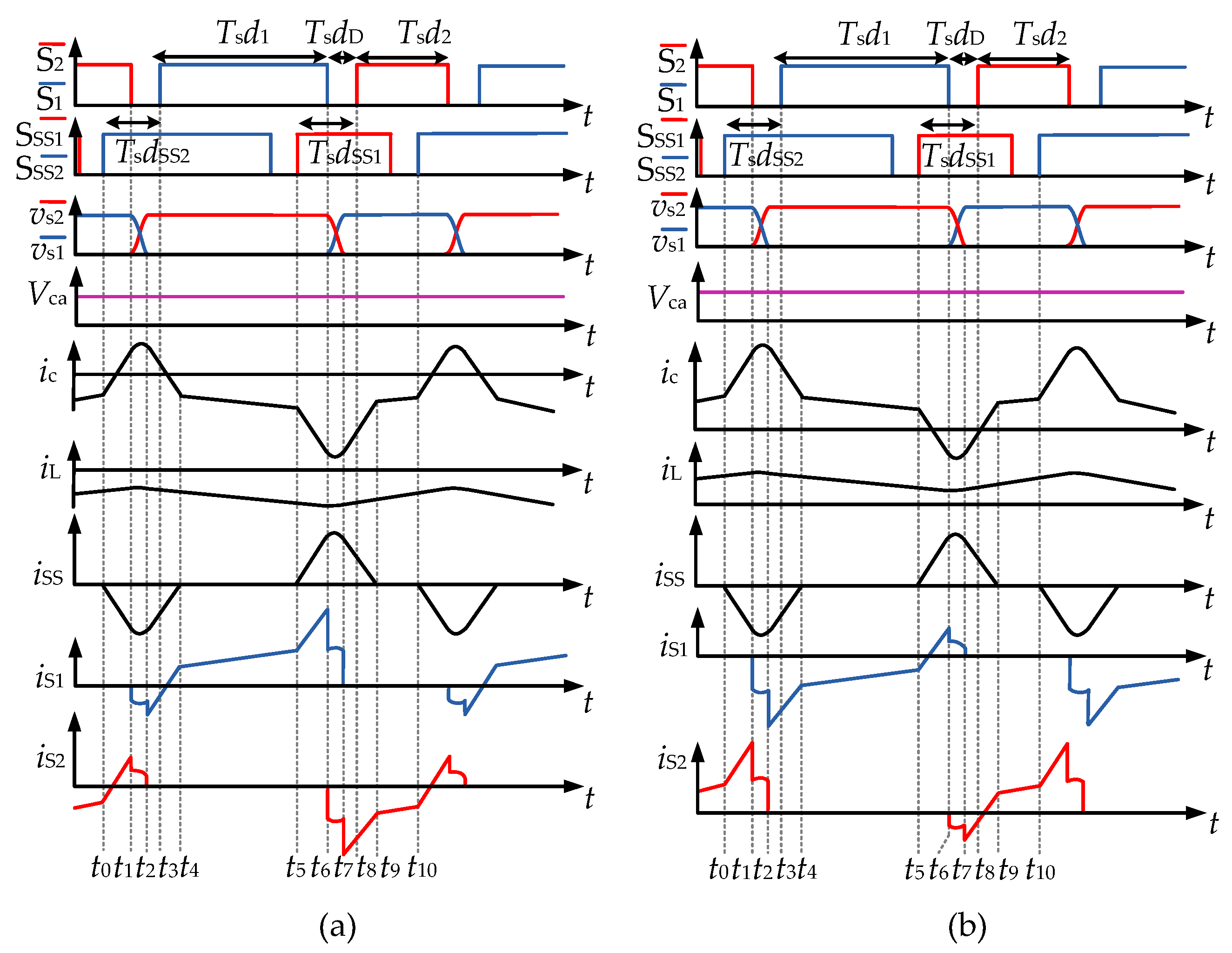
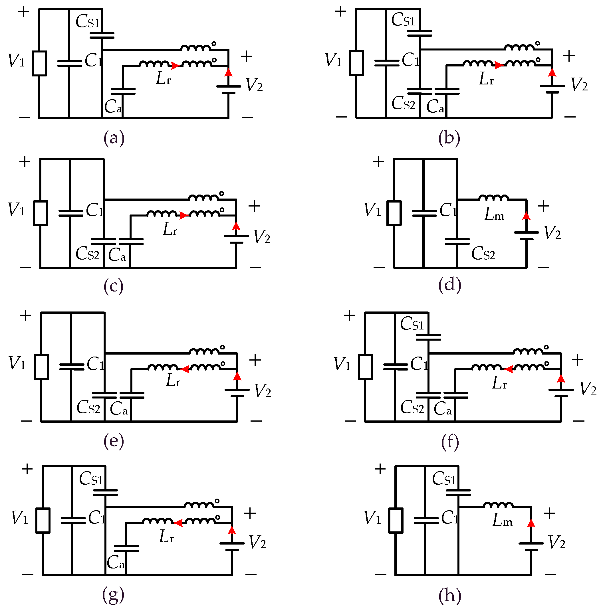
In Topology 1, as shown in Figure 2a, the switching process of each switch is shown in Figure 3. Taking the ZVS implementation of S2 as an example, the switching process is analyzed, and the equivalent circuit of each stage is shown in Figure 4.
Interval 1 [t0t1]: At t0, SSS2 is turned under the ZCS condition. The current iSS increases because of the voltage clamp action of Ca, and the equivalent circuit is shown in Figure 4a.
Interval 2 [t1t2]: At t1, S2 is turned off under the ZVS condition because of CS1 and CS2. During this interval, vS1 decreases, vS2 increases, CS1 discharges, CS2 charges, and the equivalent circuit is shown in Figure 4b. The current iSS at the resonance stage is:
i SS = i L ( t 1 ) + 2 A 11 C S ω 11 sin ( ω 11 ( t t 1 ) + θ 11 )
ω 11 = 1 2 L r C S
A 11 = V ca 2 + [ i SS ( t 1 ) i L ( t 1 ) 2 C S ω 11 ] 2
θ 11 = arctan i SS ( t 1 ) i L ( t 1 ) 2 C S ω 11 V ca + π
Interval 3 [t2t3]: At t2, vS1 decreases to 0, vS2 increases to V1, and iS1 is a negative value, the equivalent circuit for this stage is shown in Figure 4c.
Interval 4 [t3t4]: At t3, S1 is turned on under the ZVS condition.
Interval 5 [t4t5]: The current iSS is reduced to 0 at t4, and the equivalent circuit for this stage is shown in Figure 4d.
Interval 6 [t5t6]: SSS1 is turned on at t5. The current iSS increases because of the voltage clamp action of the capacitor Ca, and the equivalent circuit is shown in Figure 4e.
Interval 7 [t6t7]: S1 is turned off under ZVS condition at t6 because of CS1 and CS2. During this period, vS1 increases, vS2 decreases, CS1 charges, CS2 discharges, and the equivalent circuit is shown in Figure 4f. The auxiliary current iSS at the resonance stage is:
i SS = i L ( t 6 ) + 2 A 12 C S ω 12 sin ( ω 12 ( t t 6 ) + θ 12 )
ω 12 = 1 2 L r C S
A 12 = ( V 1 V ca ) 2 + [ i SS ( t 6 ) i L ( t 6 ) 2 C S ω 12 ] 2
θ 12 = arctan i SS ( t 6 ) i L ( t 6 ) 2 C S ω 12 ( V 1 V ca )
Interval 8 [t7t8]: At t7, vS1 increases to V1, vS2 decreases to 0, and iS2 is a negative value. The equivalent circuit for this stage is shown in Figure 4g.
Interval 9 [t8t9]: S2 is turned on under the ZVS condition at t8.
Interval 10 [t9t10]: The current iSS is reduced to 0 at t9, and the equivalent circuit for this stage is shown in Figure 4h.

2.2.2. Operation Analysis of Topology 2

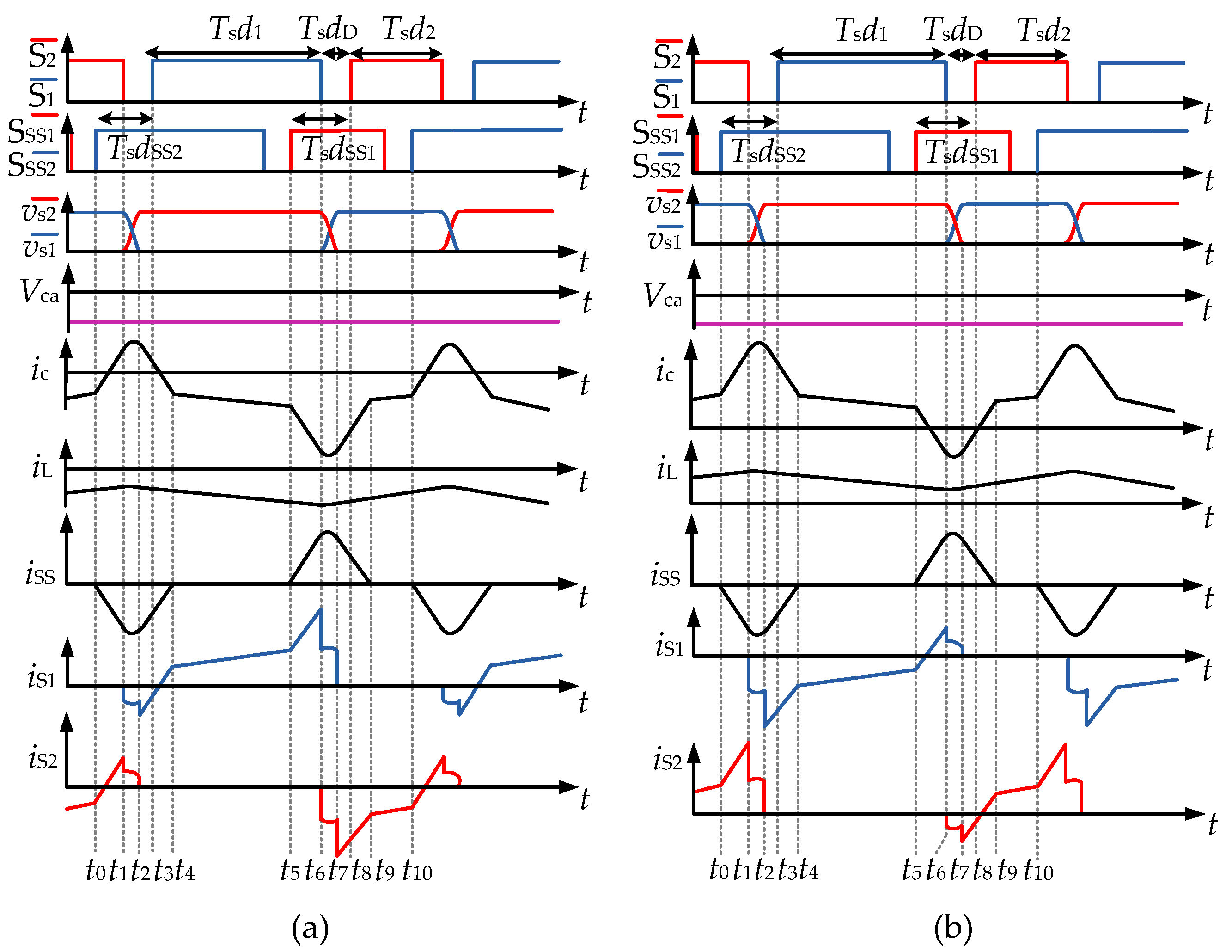
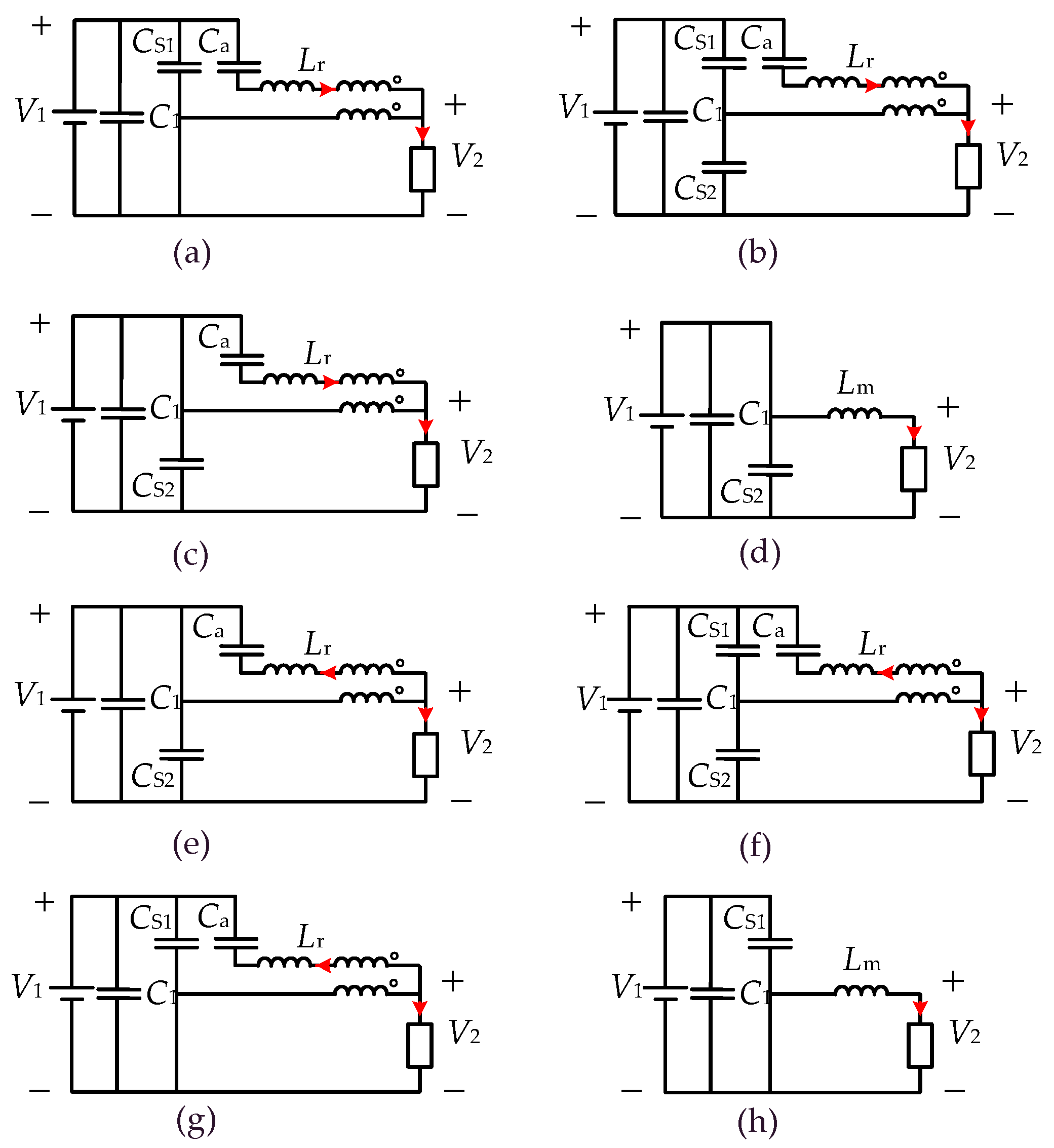
In Topology 2, as shown in Figure 2b, the switching process of each switch is shown in Figure 5. The switching process of S1 is analyzed, and the equivalent circuit of each stage is shown in Figure 6.
Interval 1 [t0t1]: At t0, SSS2 is turned on under the ZCS condition.
Interval 2 [t1t2]: At t1, S2 is turned off under the ZVS condition. The current iSS at the resonance stage is:
i SS = i L ( t 1 ) + 2 A 21 C S ω 21 sin ( ω 21 ( t t 1 ) + θ 21 )
ω 21 = 1 2 L r C S
A 21 = ( V 1 + V ca ) 2 + [ i SS ( t 1 ) i L ( t 1 ) 2 C S ω 21 ] 2
θ 21 = arctan i SS ( t 1 ) i L ( t 1 ) 2 C S ω 21 ( V 1 V ca ) + π
Interval 3 [t2t3]: At t2, vS1 decreases to 0, vS2 increases to V1, and iS1 is a negative value.
Interval 4 [t3t4]: At t3, S1 is turned on under the ZVS condition.
Interval 5 [t4t5]: S1 is on during this period.
Interval 6 [t5t6]: SSS1 is turned on under the ZCS condition at t5.
Interval 7 [t6t7]: S1 is turned off under the ZVS condition at t6. The current iSS at the resonance stage is:
i SS = i L ( t 6 ) + 2 A 22 C S ω 22 sin ( ω 22 ( t t 6 ) + θ 22 )
ω 22 = 1 2 L r C S
A 22 = V ca 2 + [ i SS ( t 6 ) i L ( t 6 ) 2 C S ω 22 ] 2
θ 22 = arctan i SS ( t 6 ) i L ( t 6 ) 2 C S ω 22 V ca
Interval 8 [t7t8]: At t7, iS2 is a negative value.
Interval 9 [t8t9]: S2 is turned on under the ZVS condition at t8.
Interval 10 [t9t10]: S2 is on during this period.

2.3. Other ZVT BDC Topologies

In addition to the topologies shown in Figure 2, other ZVT BDCs based on coupled inductor are shown in Figure 7.

3. Performance Analysis

3.1. Analysis of Input Current Ripple

As shown in Figure 3 and Figure 5, iL is nearly constant during the resonance stage (t1t2) and (t6t7), and the ripple of iL is:
Δ I L V 2 L m d 2 T S
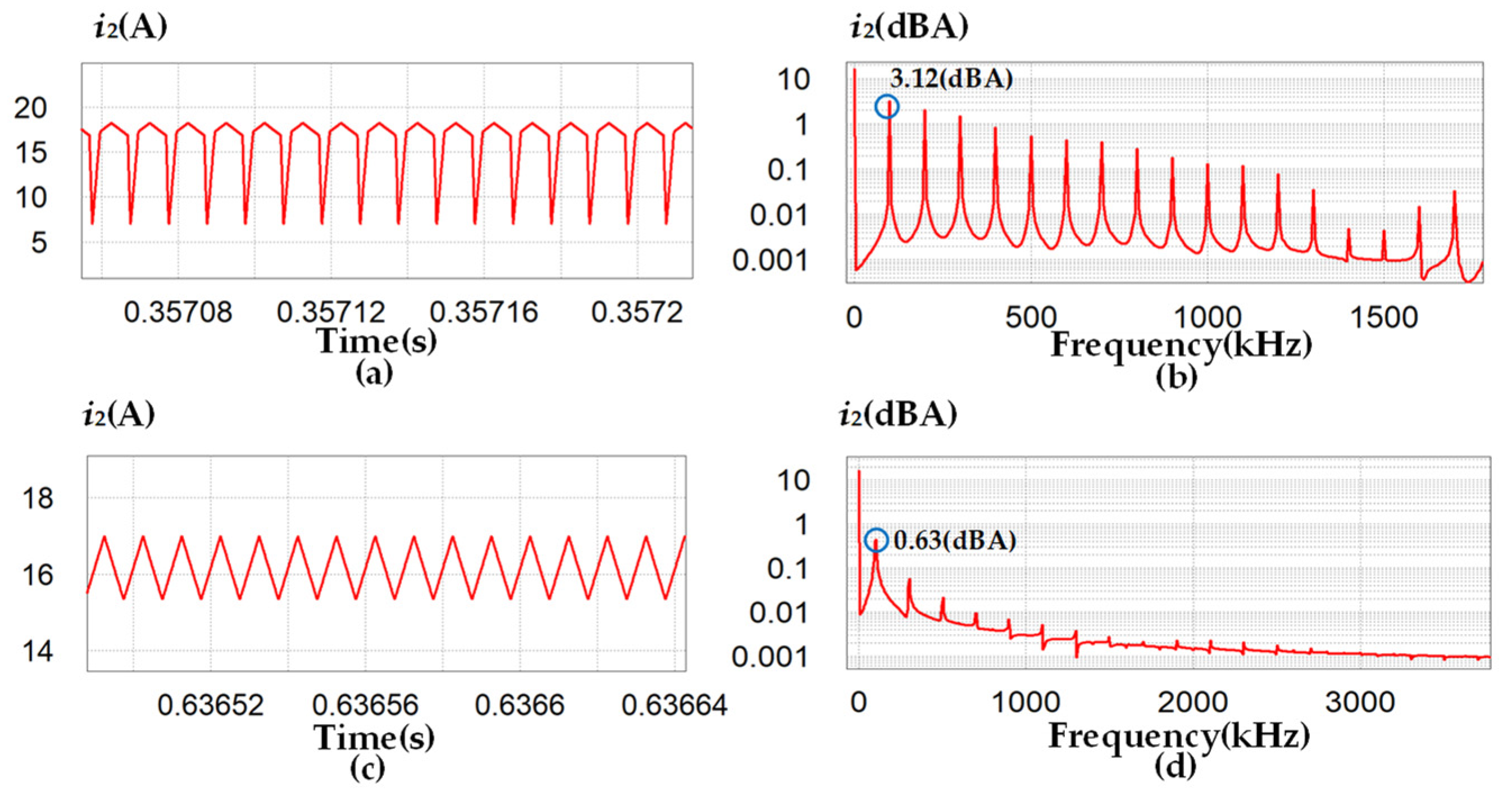
To further illustrate the advantages of the proposed ZVT BDCs, the harmonic comparison of iL is compared between the ZVT BDC (shown in Figure 2a) and the traditional ZVS BDC (represented in [23]). Those two simulation models are built, with the simulation performed at the same voltage and power levels.
The simulation results are shown in Figure 8 and Figure 9. Figure 8 shows the simulation results in Boost mode and Figure 9 in Buck mode. Figure 8a,b show the current i2 and its harmonic analysis of ZVS BDC in [23], and when P1 = 800 W, the harmonic amplitude of i2 is 3.12 dBA (100 kHz). Figure 8c,d present the simulation results of the proposed ZVT BDC; the harmonic amplitude of i2 is 0.63 dBA (100 kHz). As shown in Figure 9, when P2 = 800 W, the proposed ZVT BDC has a 1.89 dBA (100 kHz) decrease in the harmonic amplitude of i2 compared to ZVS BDC in [23].

3.2. Loss Analysis

In order to theoretically analyze the loss comparison between the traditional BDC and the proposed ZVT BDC, two simulation models are established. These work at 100 kHz and 500 kHz, respectively. The parameters are shown in Table 1, the proposed ZVT BDC is shown in Figure 2a, and the loss estimation is shown in Table 2.
For the proposed ZVT BDC, MOSFET IRFP4668 is applied as the main switch, and MOSFET SUP90142E is utilized as the auxiliary switch, respectively. The on-resistance of the main switch is 0.008 Ω, the on-resistance of the auxiliary switch is 0.017 Ω, and the diode forward voltage of the auxiliary switch is 0.85 V (the junction temperature (Tj) is 75°). The core of the coupled inductor is E220–18. In the traditional BDC model, the filter inductor adopts the magnetic core KS25060A, and the main switch adopts MOSFET IRFP4668.
For the traditional BDC, the main loss includes Pc_S (conduction loss of S1 and S2), Ps_S (switching loss of S1 and S2), core loss, and copper loss. For the proposed ZVS BDC, the main loss includes Pc_S (conduction loss of S1 and S2), Pc_SS (conduction loss of SSS1 and SSS2), PRR (Reverse recovery loss of SSS1 and SSS2), core loss, and copper loss.
When the switching frequency of the converter is increased to more than 500 kHz, the switching loss of the conventional BDC will greatly reduce the efficiency of the converter; the introduction of soft-switching measures is especially necessary.

3.3. Topology Comparison

The ZVS conditions can be realized when the circuit is operating under Buck mode or Boost mode in the ZVS BDC in [19,22,27]. Table 3 shows the topology comparison between the ZVS BDC in the existing literature and the proposed ZVS BDC (as shown in Figure 2a).
The topologies in [17,18] construct auxiliary circuits by adding auxiliary inductors, and the topology in [24] constitutes an auxiliary circuit by adding an auxiliary inductor and introducing a coupling inductor. The topologies in [19,20,21,22,23,25,26,27,28] and this paper use coupling inductors to construct auxiliary branches, which reduce the number of inductors. In order to realize soft switching in both operating modes (Buck and Boost), two auxiliary switches are required. To reduce the loss of auxiliary circuits, the diodes in [20,25,28] need to have good reverse recovery characteristics and low–forward voltage drops, which will increase the cost. In the topologies in [17,18,19,20,21,22,23,24,26], to realize the ZVT of main switches, notches exist in the current at Port 2. When Port 2 is connected to a battery, the current notch can adversely affect the battery life. However, the proposed ZVT BDC can avoid this notch phenomenon. For the topologies with no current notch in [25,28] and the proposed ZVT BDC, the current stress of the auxiliary switch depends on the current and ripple at Port 2, and the current stress is similar when the power and voltage levels are the same. In terms of voltage stress, the topology of the proposed ZVT BDC is less than that of [25].

4. System Design

4.1. Design of Initial Value Vca

4.1.1. Design of Initial Value Vca in Topology 1

For Topology 1, shown in Figure 2a, in the switching process shown in Figure 3, the resonance process should be ignored to simplify the analysis. The voltage Vca of the auxiliary capacitor Ca during the period (t0t1) is:
V ca = I SS L r t 1 t 0
During the period (t5t6), the voltage Vca of Ca is:
V ca = V 1 I SS L r t 6 t 5
When the period (t0t1) and (t5t6) are the same, the phase-shifting duty cycles of the auxiliary switch SSS1 and SSS2 are the same. According to (18) and (19), the initial value Vca = 0.5 V1 can be obtained. Considering the resonant process in the dead time, the actual Vca is different from 0.5 V1.

4.1.2. Design of Initial Value Vca in Topology 2

For Topology 2, shown in Figure 2b, the switching process is shown in Figure 5. During the period (t0t1), Vca is:
V ca = V 1 + I SS L r t 1 t 2
During the period (t5t6), Vca is:
V ca = I SS L r t 6 t 5
When the periods (t0t1) and (t5t6) are the same, the initial value Vca = −0.5 V1 can be obtained according to (20) and (21). Considering the resonant process in the dead time, the actual Vca is different from −0.5 V1.

4.2. Design of the Coupled Inductor

In the topology shown in Figure 2, the turn ratio of transformer T is n, the primary side is connected to the main circuit, the excitation inductor acts as a filter, and the secondary side is connected to the auxiliary circuit. iL is the current flowing through the excitation inductor, iSS is the current of the auxiliary circuit, iSS′ is the current converted to the primary side, and iSS′ = iSS/n. The current of Port 2 is:
i 2 = i SS + i c
The current ic is:
i c = i L i SS
According to (22) and (23), the current of port 2 is i2 = iSS + iLiSS′. Therefore, when n = 1, i2 = iL.
In the topology shown in Figure 2, Lm is the filter inductor for the BDC, duty cycle d2 is (1 − V2/V1), and the current ripple for iL is:
Δ i L V 2 L m d 2 T S
The ripple Δi2 = ΔiL, taking ΔiL = x1iL, x1 is the ripple coefficient, and the value of Lm can be obtained according to the requirement of ripple.

4.2.1. Design of Lr in Topology 1

In Topology 1, the maximum value of auxiliary current iSS is:
Δ i SSmax _ 1 = V 1 V ca L r T S d SS 1
For Buck mode, the following condition should be met to realize the ZVS of S1:
I L + 1 2 Δ i L + Δ i SSmax _ 1 > 0
For Boost mode, the following condition should be met:
I L 1 2 Δ i L Δ i SSmax _ 1 < 0
From (26) and (27), the value of Lr can be obtained.

4.2.2. Design of Lr in Topology 2

In topology 2, the maximum value of auxiliary current iSS is:
Δ i SSmax _ 2 = V ca L r T S d SS 2  
To realize the ZVS of S1 and S2, the following conditions should be satisfied:
I L + 1 2 Δ i L + Δ i SSmax _ 2 > 0
I L 1 2 Δ i L Δ i SSmax _ 2 < 0
From (29) and (30), the value of Lr can be obtained.

4.3. Design of CS

4.3.1. Design of CS in Topology 1

For Topology 1, according to the ZVS implementation process as shown in Figure 3b, dead time needs to satisfy:
Δ t 12 = t 2 t 1 = 1 ω 11 ( arccos V ca A 11 arccos V 1 V ca A 11 ) < t D
Δ t 67 = t 7 t 6 = 1 ω 12 ( arccos V ca A 12 arccos V 1 V ca A 12 ) < t D
At time t7, the values of ic and iS2 are:
i c ( t 7 ) = 2 A 12 C S ω 12 sin ( ω 12 ( t 7 t 6 ) + θ 12 )
i S 2 ( t 7 ) = A 12 C S ω 12 sin ( ω 12 ( t 7 t 6 ) + θ 12 )
When S2 is turned on, iS2 needs to meet:
i S 2 ( t S 2 _ on ) = i S 2 ( t 7 ) + ( V ca L r + V 2 L m ) × ( t D Δ t 67 ) < 0
According to (31)–(35),the value of CS can be obtained.

4.3.2. Design of CS in Topology 2

For Topology 2, according to the ZVS implementation process as shown in Figure 5a, in order to realize the ZVS of S1, the following conditions should be met:
Δ t 12 = t 2 t 1 = 1 ω 21 ( arccos V 1 V ca A 21 arccos V ca A 21 ) < t D
Δ t 67 = t 7 t 6 = 1 ω 22 ( arccos V 1 V ca A 22 arccos V ca A 22 ) < t D
i S 1 ( t S 1 _ on ) = i S 1 ( t 2 ) + ( V ca L r + V 1 V 2 L m ) × ( t D Δ t 12 ) < 0
According to (36)–(38), the value of CS can be obtained.

4.4. Design of Ca

4.4.1. Design of Ca in Topology 1

As the voltage source of the auxiliary circuit, the voltage Vca of the auxiliary capacitor Ca can be determined according to the duration of (t0t1) and (t5t6), and the voltage ripple ΔVca is:
Δ V ca = 1 C a t 0 T s 2 i SS ( t ) d t
In order to simplify the analysis, ignoring the resonance process and according to (39) and Figure 3, ΔVca can be obtained:
Δ V ca V 1 V ca T S 2 d SS 2 2 2 C a L r ( V 1 V ca )
Taking ΔVca = x2Vca, x2 is the voltage ripple coefficient, and the value of auxiliary capacitance Ca can be obtained according to the requirement of voltage ripple.

4.4.2. Design of Ca in Topology 2

According to (39), and Figure 5, ΔVca can be obtained:
Δ V ca V 1 ( V 1 + V ca ) T S 2 d SS 2 2 2 C a L r V ca
Similarly, according to the ripple requirements, the value of the auxiliary capacitor Ca can be obtained.
Taking the ZVT BDC (as shown in Figure 2a) design process as an example, a step-by-step design methodology working in Boost mode is given in Table 4. The other topologies and the design process in Buck mode are similar and will not be repeated.

4.5. Design of the Control Method

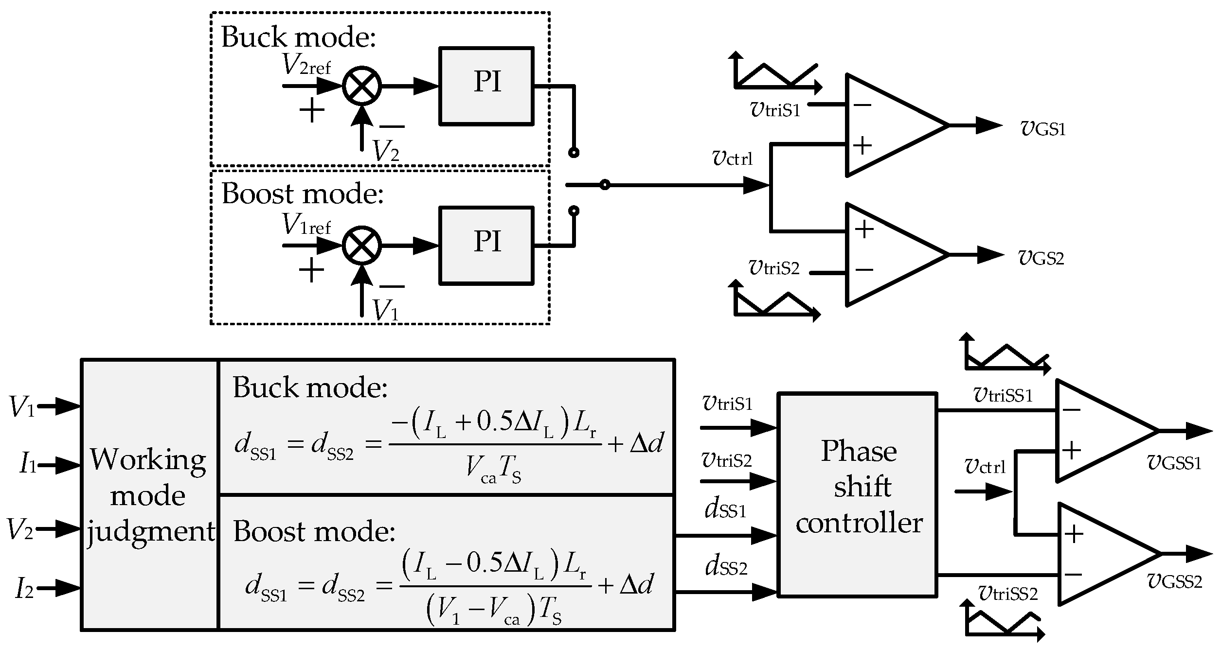
Figure 10 shows the implementation of the control method, which is divided into two cases (Buck mode and Boost mode). The PI regulator of the output voltage (V2 under Buck, V1 in Boost) generates the modulation signal vctrl, and the phase difference between the carrier signals vtriS1 and vtriS2 is 180°, generating the drive signals of S1 and S2 by comparators. To obtain the driving signals of SSS1 and SSS2, firstly, judge the working mode of the system (Buck mode or Boost mode) according to the voltages and currents of Ports 1 and 2. The phase-shifting duty cycles dSS1 and dSS2 are calculated according to the working mode. In order to ensure that the auxiliary current is large enough, dSS1 and dSS2 require a certain amount of margin Δd. The phase-shifting controller shifts the carrier signals vtriS1 and vtriS2 according to dSS1 and dSS2, and the carrier signals of SSS1 and SSS2, vtriSS1 and vtriSS2, are obtained. The driving signals of SSS1 and SSS2 are generated by comparators.

5. Experimental Verification

Using DSP TMS320F28377SPTPT as the controller, MOSFET IRFP4668 as the main switch, and MOSFET SUP90142E as the auxiliary switch, a BDC prototype is built, as shown in Figure 11. Detailed experimental parameters are shown in Table 5.
To verify the validity of the two ZVT BDCs shown in Figure 2, two sets of experiments were conducted, in each set of experiments; the power level is 800 W. The experimental waveforms of these two topologies operating in two modes (Buck and Boost) and two duty cycles (d1 = 0.4 and d1 = 0.6) are given. The control method utilized in the experiments is shown in Figure 10.
Figure 12, Figure 13, Figure 14 and Figure 15 show the experimental waveforms of the topology shown in Figure 2a.
When ZVS BDC operates in Boost mode, P1 = 800 W, V1 = 100 V, Figure 12 and Figure 13 are the experimental waveforms under the condition of V2 = 40 V and V2 = 60 V, respectively. The main switches S1 and S2 are turned on and off under ZVS conditions, and the auxiliary switches SSS1 and SSS2 are turned on and off under ZCS conditions. When V2 is 40 V and 60 V, in order to achieve the ZVS of S2, the phase shift angles between the drive signals vGSS1 and vG2 can be 60° and 45°, respectively.
When ZVS BDC operates in Buck mode, P2 = 800 W, V1 = 100 V, Figure 14 and Figure 15 are the experimental waveforms under the condition of V2 = 40 V and V2 = 60 V, respectively. The main switches S1 and S2, are turned on and off under ZVS conditions, and the auxiliary switches SSS1 and SSS2 are turned on and off under ZCS conditions. When V2 is 40 V and 60 V, in order to achieve the ZVS of S1, the phase shift angles between the drive signals vGSS2 and vG1 can be 60° and 45°, respectively.
Figure 16, Figure 17, Figure 18 and Figure 19 show the experimental waveforms of the topology shown in Figure 2b.
When ZVS BDC operates in Boost mode, P1 = 800 W, V1 = 100 V, Figure 16 and Figure 17 are the experimental waveforms under the condition of V2 = 40 V and V2 = 60 V, respectively. The main switches S1 and S2 are turned on and off under ZVS conditions, and the auxiliary switches SSS1 and SSS2 are turned on and off under ZCS conditions. When V2 is 40 V and 60 V, in order to achieve the ZVS of S2, the phase shift angles between the drive signals vGSS1 and vG2 can be 60° and 45°, respectively.
When ZVS BDC operates in Buck mode, P2 = 800 W, V1 = 100 V, Figure 18 and Figure 19 are the experimental waveforms under the condition of V2 = 40 V and V2 = 60 V, respectively. The main switches S1 and S2 are turned on and off under ZVS conditions, and the auxiliary switches SSS1 and SSS2 are turned on and off under ZCS conditions. When V2 is 40 V and 60 V, in order to achieve the ZVS of S1, the phase shift angles between the drive signals vGSS2 and vG1 can be 60° and 45°, respectively.
As shown in Figure 12, Figure 13, Figure 14, Figure 15, Figure 16, Figure 17, Figure 18 and Figure 19, the current at Port 2 has no notch when these two proposed ZVT BDCs operate in both two modes (Buck and Boost). In Topology 1, Vca > 0, and in Topology 2, Vca < 0. When the power circuit operates in Buck mode, the current ic flowing through the bridge arm (S1 and S2) changes from negative to positive before S1 is turned on due to the auxiliary current. When the power circuit operates in Boost mode, ic changes from positive to negative before S2 is turned on, realizing ZVT conditions for S1 and S2. When the average value of i2 changes, the peak of iSS has different requirements. Thus, dSS1 and dSS2 need to be adjusted. In addition, auxiliary switches are turned on and off under ZCS conditions.
As shown in Figure 20, the main loss sources of a traditional BDC include conduction loss of the main switch, switching loss of the main switch, copper loss and core loss of the inductor. The main loss sources of the proposed ZVS BDC include the conduction loss of the main switch, conduction loss of the auxiliary switch, RR loss of the auxiliary switch, copper loss, and core loss of inductor. For the traditional BDC topology, switching loss accounts for the largest proportion of the total loss, while for the proposed BDC, the largest source is conduction loss. As shown in Figure 21, compared to the traditional BDC, the maximum efficiency of the proposed BDC (shown in Figure 2a) can be improved by 1.2%.
Through the theoretical analysis of the loss of traditional BDC, when the switching frequency is increased to more than 500 kHz, it is necessary to introduce the ZVT implementation measures. According to the efficiency curve of the existing topology, the loss analysis is carried out when the switching frequency is greater than 500 kHz, and the comparison of the theoretical efficiency values among different topologies under full load when the switching frequency fS ≥ 500 kHz is shown in Table 6.

6. Conclusions

In this paper, several ZVT magnetic coupling BDCs are proposed. In these topologies, the excitation inductor of the transformer acts as a filter, and the leakage inductor is used to generate auxiliary current. When the turn ratio is 1:1, the current of the original side and the secondary side is the same but in the opposite direction. Thus, the current notch at the low voltage port can be eliminated. The main switches can achieve ZVT conditions, and the auxiliary switches can achieve ZCS conditions. In order to verify the feasibility of these ZVT BDCs, 100-kHz and 800-W prototypes are built, and the experimental results of two working modes (Boost and Buck) are shown. Through detailed theoretical analysis and experimental verification, all switches of the converter realize soft switching, and no current notch exists at the low-voltage port. Compared with the traditional BDC, the maximum efficiency can be increased by 1.2%.

Author Contributions

Conceptualization, S.W.; methodology, S.W., M.G. and J.S.; validation, S.W. and M.G. All authors have read and agreed to the published version of the manuscript.

Funding

This work is supported by the National Natural Science Foundation of China (52077199).

Data Availability Statement

Not applicable.

Conflicts of Interest

The authors declare no conflict of interest.

References

  1. Lee, H.; Yun, J. High-Efficiency Bidirectional Buck–Boost Converter for Photovoltaic and Energy Storage Systems in a Smart Grid. IEEE Trans. Power Electron. 2019, 34, 4316–4328. [Google Scholar] [CrossRef]
  2. Mirzaei, A.; Forooghi, M.; Ghadimi, A.A.; Abolmasoumi, A.H.; Riahi, M.R. Design and construction of a charge controller for stand-alone PV/battery hybrid system by using a new control strategy and power management. Sol. Energy 2017, 149, 132–144. [Google Scholar] [CrossRef]
  3. Dimitrov, B.; Hayatleh, K.; Barker, S.; Collier, G.; Sharkh, S.; Cruden, A. A Buck–Boost Transformerless DC–DC Converter Based on IGBT Modules for Fast Charge of Electric Vehicles. Electronics 2020, 9, 397. [Google Scholar] [CrossRef] [Green Version]
  4. Park, D.-R.; Kim, Y. Design and Implementation of Improved High Step-Down DC–DC Converter for Electric Vehicles. Energies 2021, 14, 4206. [Google Scholar] [CrossRef]
  5. Abusara, M.A.; Guerrero, J.M.; Sharkh, S.M. Line-Interactive UPS for Microgrids. IEEE Trans. Ind. Electron. 2013, 61, 1292–1300. [Google Scholar] [CrossRef] [Green Version]
  6. Wu, J.; Wen, P.; Sun, X.; Yan, X. Reactive Power Optimization Control for Bidirectional Dual-Tank Resonant DC–DC Converters for Fuel Cells Systems. IEEE Trans. Power Electron. 2020, 35, 9202–9214. [Google Scholar] [CrossRef]
  7. Ramirez-Murillo, H.; Restrepo, C.; Konjedic, T.; Calvente, J.; Romero, A.; Baier, C.R.; Giral, R. An Efficiency Comparison of Fuel-Cell Hybrid Systems Based on the Versatile Buck–Boost Converter. IEEE Trans. Power Electron. 2018, 33, 1237–1246. [Google Scholar] [CrossRef]
  8. Huang, X.; Lee, F.C.; Li, Q.; Du, W. High-Frequency High-Efficiency GaN-Based Interleaved CRM Bidirectional Buck/Boost Converter with Inverse Coupled Inductor. IEEE Trans. Power Electron. 2016, 31, 4343–4352. [Google Scholar] [CrossRef]
  9. Yao, Z.; Lu, S. A Simple Approach to Enhance the Effectiveness of Passive Currents Balancing in an Interleaved Multiphase Bidirectional DC–DC Converter. IEEE Trans. Power Electron. 2019, 34, 7242–7255. [Google Scholar] [CrossRef]
  10. Ahmed, H.F.; Cha, H.; Kim, S.; Kim, D.; Kim, H. Wide Load Range Efficiency Improvement of a High-Power-Density Bidirectional DC–DC Converter Using an MR Fluid-Gap Inductor. IEEE Trans. Ind. Appl. 2015, 51, 3216–3226. [Google Scholar] [CrossRef]
  11. Jayashree, E.; Uma, G. Design and implementation of zero-voltage switching quasi-resonant positive-output Luo converter using analog resonant controller UC3861. IET Power Electron. 2011, 4, 81–88. [Google Scholar] [CrossRef]
  12. Moradisizkoohi, H.; Elsayad, N.; Mohammed, O.A. Experimental Demonstration of a Modular, Quasi-Resonant Bidirectional DC-DC Converter Using GaN Switches for Electric Vehicles. IEEE Trans. Ind. Appl. 2019, 55, 7787–7803. [Google Scholar] [CrossRef]
  13. Liu, S.; Wu, X. A 1-MHz ZVS Boost DC–DC converter with active clamping using GaN power transistors. In Proceedings of the 2016 IEEE 8th International Power Electronics and Motion Control Conference (IPEMC-ECCE Asia), Hefei, China, 22–26 May 2016; pp. 557–562. [Google Scholar]
  14. Lee, S.S.; Choi, S.W.; Moon, G.W. High efficiency active clamp forward converter with synchronous switch controlled ZVS operation. J. Power Electron. 2006, 6, 131–138. [Google Scholar]
  15. Lee, I.; Kim, J.; Lee, T.; Jung, Y.; Won, C. A new bidirectional DC–DC converter with ZVT switching. In Proceedings of the 2012 IEEE Vehicle Power and Propulsion Conference (VPPC), Seoul, Republic of Korea, 9–12 October 2012; pp. 684–689. [Google Scholar]
  16. Yang, J.; Do, H. High-Efficiency Bidirectional DC–DC Converter With Low Circulating Current and ZVS Characteristic Throughout a Full Range of Loads. IEEE Trans. Ind. Electron. 2014, 61, 3248–3256. [Google Scholar] [CrossRef]
  17. Mohammadi, M.R.; Farzanehfard, H. Analysis of Diode Reverse Recovery Effect on the Improvement of Soft-Switching Range in Zero-Voltage-Transition Bidirectional Converters. IEEE Trans. Ind. Electron. 2015, 62, 1471–1479. [Google Scholar] [CrossRef]
  18. Lee, J.H.; Yu, D.H.; Kim, J.G.; Kim, Y.H.; Won, C.Y. Auxiliary Switch Control of a Bidirectional Soft-Switching DC/DC Converter. IEEE Trans. Power Electron. 2013, 28, 5446–5457. [Google Scholar] [CrossRef]
  19. Zhang, Y.; Sen, P.C. A new soft-switching technique for buck, boost, and buck–boost converters. IEEE Trans. Ind. Appl. 2003, 39, 1775–1782. [Google Scholar] [CrossRef]
  20. Mohammadi, M.R.; Farzanehfard, H. New Family of Zero-Voltage-Transition PWM Bidirectional Converters with Coupled Inductors. IEEE Trans. Ind. Electron. 2012, 59, 912–919. [Google Scholar] [CrossRef]
  21. Mohammadi, M.R.; Farzanehfard, H. A New Family of Zero-Voltage-Transition Nonisolated Bidirectional Converters with Simple Auxiliary Circuit. IEEE Trans. Ind. Electron. 2016, 63, 1519–1527. [Google Scholar] [CrossRef]
  22. Chen, G.; Deng, Y.; Tao, Y.; He, X.; Wang, Y.; Hu, Y. Topology Derivation and Generalized Analysis of Zero-Voltage-Switching Synchronous DC–DC Converters With Coupled Inductors. IEEE Trans. Ind. Electron. 2016, 63, 4805–4815. [Google Scholar] [CrossRef]
  23. Chen, G.; Deng, Y.; Chen, L.; Hu, Y.; Jiang, L.; He, X.; Wang, Y. A Family of Zero-Voltage-Switching Magnetic Coupling Nonisolated Bidirectional DC–DC Converters. IEEE Trans. Ind. Electron. 2017, 64, 6223–6233. [Google Scholar] [CrossRef]
  24. Mohammadi, M.R.; Farzanehfard, H. Family of Soft-Switching Bidirectional Converters With Extended ZVS Range. IEEE Trans. Ind. Electron. 2017, 64, 7000–7008. [Google Scholar] [CrossRef]
  25. Mohammadi, M.R.; Peyman, H.; Yazdani, M.R.; Mirtalaei, S.M.M. A ZVT Bidirectional Converter With Coupled-Filter-Inductor and Elimination of Input Current Notches. IEEE Trans. Ind. Electron. 2020, 67, 7461–7469. [Google Scholar] [CrossRef]
  26. Nan, C.; Ayyanar, R. A 1 MHz Bi-directional Soft-switching DC–DC Converter with Planar Coupled Inductor for Dual Voltage Automotive Systems. In Proceedings of the 2016 IEEE Applied Power Electronics Conference and Exposition (APEC), Long Beach, CA, USA, 20–24 March 2016; pp. 432–439. [Google Scholar]
  27. Cheng, X.; Zhang, Y.; Yin, C. A Family of Coupled-Inductor-Based Soft-Switching DC–DC Converter With Double Synchronous Rectification. IEEE Trans. Ind. Electron. 2019, 66, 6936–6946. [Google Scholar] [CrossRef]
  28. Wang, S.; Hu, Y.; Gao, M.; Shi, J. Coupled inductor based zero-voltage-switching buck/boost converter. J. Power Electron. 2022, 22, 1059–1072. [Google Scholar] [CrossRef]
  29. Rezvanyvardom, M.; Mirzaei, A. Zero-Voltage Transition Nonisolated Bidirectional Buck–Boost DC–DC Converter With Coupled Inductors. IEEE J. Emerg. Sel. Top. Power Electron. 2021, 9, 3266–3275. [Google Scholar] [CrossRef]
  30. Cheng, X.; Liu, C.; Wang, D.; Zhang, Y. State-of-the-Art Review on Soft-Switching Technologies for Non-Isolated DC-DC Converters. IEEE Access 2021, 9, 119235–119249. [Google Scholar] [CrossRef]
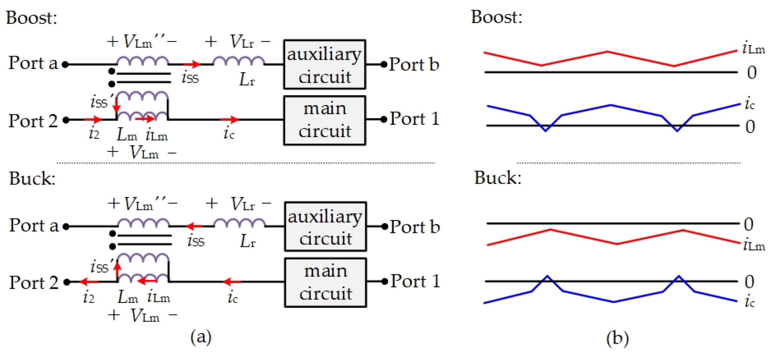
Figure 1. General circuit of ZVS BDCs with coupled filter inductors in [20,21,23,24,26]. (a) General circuit; (b) key waveforms of the input currents.
Energies 16 04760 g001
Figure 2. The proposed ZVS BDCs. (a) Topology 1; (b) Topology 2.
Energies 16 04760 g002
Figure 3. ZVS implementation of the main switch for topology 1. (a) ZVS implementation of S1; (b) ZVS implementation of S2.
Energies 16 04760 g003
Figure 4. The equivalent circuit for each stage of Topology 1. (a) t0t1; (b) t1t2; (c) t2t4; (d) t4t5; (e) t5t6; (f) t6t7; (g) t7t9; (h) t9t10.
Energies 16 04760 g004
Figure 5. ZVS implementation of the main switch for Topology 2. (a) ZVS implementation of S1; (b) ZVS implementation of S2.
Energies 16 04760 g005
Figure 6. The equivalent circuit for each stage of Topology 2. (a) t0t1; (b) t1t2; (c) t2t4; (d) t4t5; (e) t5t6; (f) t6t7; (g) t7t9; (h) t9t10.
Energies 16 04760 g006
Figure 7. Other ZVT BDCs. (a) Topology 1; (b) Topology 2.
Energies 16 04760 g007
Figure 8. Harmonic comparison in Boost mode. (a) Input current of ZVS BDC in [23]; (b) harmonic analysis of input current of ZVS BDC in [23]; (c) input current of ZVT BDC (shown in Figure 2a); (d) harmonic analysis of input current of ZVT BDC (shown in Figure 2a).
Energies 16 04760 g008
Figure 9. Harmonic comparison in Buck mode. (a) Output current of ZVS BDC in [23]; (b) harmonic analysis of output current of ZVS BDC in [23]; (c) output current of ZVT BDC (shown in Figure 2a); (d) harmonic analysis of output current of ZVT BDC (shown in Figure 2a).
Energies 16 04760 g009
Figure 10. Control schematic diagram.
Energies 16 04760 g010
Figure 11. Experimental platform.
Energies 16 04760 g011
Figure 12. Experimental waveforms of BDC Topology 1 when P1 = 800 W, V1 = 100 V, d1 = 0.4 (t − 2 μs/div). (a) vDS2, vGS2, and ic; (b) vDS1, vGS1, and i2; (c) vGSS1, vGS2, and iSS; (d) V1, V2, and Vca.
Energies 16 04760 g012
Figure 13. Experimental waveforms of BDC Topology 1 when P1 = 800 W, V1 = 100 V, d1 = 0.6 (t − 2 μs/div). (a) vDS2, vGS2, and ic; (b) vDS1, vGS1, and i2; (c) vGSS1, vGS2, and iSS; (d) V1, V2, and Vca.
Energies 16 04760 g013
Figure 14. Experimental waveforms of BDC Topology 1 when P2 = 800 W, V1 = 100 V, d1 = 0.4 (t − 2 μs/div). (a) vDS1, vGS1, and ic; (b) vDS2, vGS2, and i2; (c) vGSS2, vGS1, and iSS; (d) V1, V2, and Vca.
Energies 16 04760 g014
Figure 15. Experimental waveforms of BDC Topology 1 when P2 = 800 W, V1 = 100 V, d1 = 0.6 (t − 2 μs/div). (a) vDS1, vGS1, and ic; (b) vDS2, vGS2, and i2; (c) vGSS2, vGS1, and iSS; (d) V1, V2, and Vca.
Energies 16 04760 g015
Figure 16. Experimental waveforms of BDC Topology 2 when P1 = 800 W, V1 = 100 V, d1 = 0.4 (t – 2 μs/div). (a) vDS2, vGS2, and ic; (b) vDS1, vGS1, and i2; (c) vGSS1, vGS2, and iSS; (d) V1, V2, and Vca.
Energies 16 04760 g016
Figure 17. Experimental waveforms of BDC Topology 2 when P1 = 800 W, V1 = 100 V, d1 = 0.6 (t – 2 μs/div). (a) vDS2, vGS2, and ic; (b) vDS1, vGS1, and i2; (c) vGSS1, vGS2, and iSS; (d) V1, V2, and Vca.
Energies 16 04760 g017
Figure 18. Experimental waveforms of BDC Topology 2 when P2 = 800 W, V1 = 100 V, d1 = 0.4 (t – 2 μs/div). (a) vDS1, vGS1, and ic; (b) vDS2, vGS2, and i2; (c) vGSS2, vGS1, and iSS; (d) V1, V2, and Vca.
Energies 16 04760 g018
Figure 19. Experimental waveforms of BDC Topology 2 when P2 = 800 W, V1 = 100 V, d1 = 0.6 (t – 2 μs/div). (a) vDS1, vGS1, and ic; (b) vDS2, vGS2, and i2; (c) vGSS2, vGS1, and iSS; (d) V1, V2, and Vca.
Energies 16 04760 g019
Figure 20. Loss analysis.
Energies 16 04760 g020
Figure 21. Efficiency curves with and without auxiliary circuit. (a) Boost; (b) Buck.
Energies 16 04760 g021
Table 1. Detail parameters of 800 W ZVS Boost converter.
fS = 100 kHzfS = 500 kHz
ParameterValueParameterValueParameterValueParameterValue
V2/V50V1/V100V2/V50V1/V100
P1max/W800n1P1max/W800n1
Lc/μH3.8Lm/μH130Lc/μH0.85Lm/μH160
C1/μF1000C2/μF1000C1/μF1000C2/μF1000
CS/nF2.2Ca/μF200 CS/nF1Ca/μF80
Table 2. Loss comparison.
Loss SourcefS = 100 kHzfS = 500 kHz
Traditional BDCProposed BDCTraditional BDCProposed BDC
Pc_S2.1 W2.5 W2.1 W3.1 W
Pc_SS---5.4 W---10.4 W
Ps_S19.1 W---95.5 W---
PRR---0.8 W---4.2 W
Core loss1.9 W2.1 W0.3 W0.4 W
Copper loss2.7 W3.3 W2.9 W4.3 W
Table 3. Topology comparison.
TopologyNumber of Auxiliary SwitchesNumber of Auxiliary DiodesCurrent NotchVoltage Stress of Auxiliary Switches
ZVT BDC [17]22existmax{DV1, (1 − D)V1}
ZVS BDC [18]20existBuck: V2
Boost: V1V2
ZVT BDC [20]22exist(1 + nD)V2
ZVT BDC [21]20existnDV1
ZVS BDC [23]20existSa1: (n + 1)V2
Sa2: (n + 1)( V1V2)
ZVS BDC [24]22existBuck: max{|(n − 1)(V1V2)|, V2 + n(V1V2)}
Boost: max{|(n − 1)V2|, V1 + (n − 1)V2}
ZVT BDC [25]22noBuck: >0.5 V2
Boost: >0.5 V2
ZVT BDC [26]20existSa1: (n + 1)(V1V2)
Sa2: (n + 1)V2
ZVS BDC [28]22noSSS1: 2 3 [ L 1 ( V 1 V 2 ) L 1 + L c 2 M + V 2 ] 1 3 V 1
SSS2: 2 3 ( L c M ) V 2 L 1 + L c 2 M + 1 3 V 1
Proposed ZVT BDCs20noSSS1: V1Vca
SSS2: Vca
Table 4. Step-by-step design methodology.
Step 1Determine the voltages (V1 and V2) and power level according to the system requirements.
Step 2Ignore the resonance process and select initial value of Vca, Vca = 0.5V1.
Step 3Design Lm of T according to the requirements of current ripple, and L m V 2 d 2 T S x 1 I L .
Step 4Select n = 1.
Step 5Design Lr of T according to IL − 0.5ΔiL − ΔiSS < 0, in which Δ i SS = V 1 V ca L r T S d SS 1 .
Step 6Determine value range of (CS, td) according to { t 12 < t d t 67 < t d i S 2 ( t S 2 _ on ) < 0 , and select CS and td.
Step 7Design Ca according to the requirements of voltage ripple, and C a 1 x 2 V ca t 0 T s 2 i SS ( t ) d t .
Step 8Simulation and experimental verification.
Table 5. Detail parameters of experimental platform.
ParameterValueParameterValue
V2/V40~60V1/V100
fS/kHz100n1
Lc/μH3.8Lm/μH130
C1 and C2/μF1000CS/nF2.2
P1max and P2max/W800Ca/μF200
Table 6. Efficiency comparison when the switching frequency fS ≥ 500 kHz.
TopologyBoostBuck
ZVS BDC [17]96.7%95.2%
ZVS BDC [18]97.2%96.5%
ZVT BDC [20]95.7%95.6%
ZVT BDC [21]97.7%97.2%
ZVS BDC [23]97.5%97.5%
ZVS BDC [24]96.3%96.5%
ZVT BDC [25]95.3%95.4%
ZVT BDC [26]92.2%93.3%
ZVS BDC [28]96.4%96.2%
The proposed ZVT BDCs96.7%96.7%
Disclaimer/Publisher’s Note: The statements, opinions and data contained in all publications are solely those of the individual author(s) and contributor(s) and not of MDPI and/or the editor(s). MDPI and/or the editor(s) disclaim responsibility for any injury to people or property resulting from any ideas, methods, instructions or products referred to in the content.