1. Introduction
Resonant DC-DC converters operating above the resonant frequency are characterized by a high efficiency and an operational reliability. They are becoming an increasingly preferred source of high-frequency power for the needs of various industrial applications such as renewable energy applications [
1], contactless energy transmission systems [
2], electric vehicle applications [
3,
4], etc. LLC resonant converters, which are part of the resonant converters, have been widely discussed in recent years due to the advantages they possess and possibilities for applications in EV chargers [
5,
6], LED lighting applications [
7,
8,
9] and various other applications [
10]. An important design advantage of LLC topologies over other types of resonant converters is the possibility to implement the two inductances (series and parallel) practically in only one component, the matching transformer [
11].
Many of the properties and characteristics of LLC resonant DC-DC converters are determined by the methods used for their control [
12]. Widely used is the output power control method, based on changing the control frequency of the transistors in the inverter part of the circuit [
13]. The frequency control method (FM) is easy to implement and can handle discontinuous currents, but it is characterized by slow dynamic response. Phase-shift control is another usable control method [
14,
15,
16,
17]. It is also easy to implement and allows operation at a constant frequency, but the efficiency is lowered at high loads. In [
18], a disturbance-observer-based control for phase-shift LLC converters was introduced to improve the dynamic performances under large input voltages and load variations due to the strong nonlinearity of the LLC converter and difficulties using typical linear control methods.
Some authors propose using hybrid control methods to overcome the disadvantages of the FM and phase-shift control strategies. In [
12,
19], an LLC resonant DC-DC converter for a hybrid power system was considered, controlled by a frequency modulation and phase-shift control strategy. According to [
20], a hybrid control method was also discussed that combines FM mode and PWM mode depending on the load conditions.
Another strategy, named the Bang-Bang Charge Control method for LLC resonant converters, was presented in [
21]. The series capacitor voltage and a pair of threshold voltages were used to determine the switching instants of the transistors. The method provided sub-optimal trajectory since the controller did not calculate the new steady state. Fast feedback was used to bring the converter closer to the new steady state.
However, to achieve a fast transient response, an optimal trajectory control method was initially performed in [
22] for series resonant converters. Due to the increased number of state variables and operating modes in the LLC converter circuit, this control is more complicated to implement. In [
23], an application of the optimal trajectory control method for LED PWM dimming was presented.
Optimal trajectory control has several advantages compared with the other control methods: a reduction in overvoltages of reactive and switching elements in the circuit, and fast dynamic response in cases of significant changes in converter operating conditions without affecting the stability of the whole system. A disadvantage of the method is the necessity to calculate in real time a nonlinear function that defines all the energy stored in the resonant circuit.
In [
24,
25], a simplified optimal trajectory control for LLC converters was presented by assuming that the switching frequency equaled the resonant frequency. Thus, very fast dynamic performances were achieved, but the influence on the operation at other switching frequencies needs to be discussed.
A simple control method for a series resonant converter was proposed in [
26] to achieve characteristics similar to an optimal trajectory controlled converter. At the same time, it reduced the complexity of this control technique. The significant simplification of the discussed control technique was mainly due to the linearization of the control function around the switching point.
On the basis of this concept, the present article proposes a simple trajectory control for an LLC resonant converter, ensuring a behavior similar to that with optimal trajectory control. Furthermore, the large number of state variables usually used for implementing optimal trajectory control in LLC resonant converters is reduced, and the control technique is simplified.
The main objective of the paper is the study converter’s behavior by obtaining normalized output, control and load characteristics operating above its series resonant frequency. These characteristics, required for the LLC resonant converter design and application, are built for the different inductance ratios. The boundaries, at which the simple trajectory control method is valid, are defined. A functional model of an LLC resonant converter controlled by the considered method is presented and implemented using the principle of Analog Behavioral Modeling (ABM) embedded in the PSpice for TI simulator. A simulation of the converter’s behavior is performed and compared with the analytically obtained results.
2. Converter Operation Using a Simple Control Technique
Figure 1 shows a circuit diagram of the considered full-bridge configuration of an LLC DC-DC converter. It consists of an inverter part (transistors
S1 ÷
S4 and anti-parallel diodes
D1 ÷
D4), a series resonant circuit (
Ls and
Cs), a parallel inductance
LP, a matching transformer (
Tr), an uncontrolled rectifier (
D5 ÷
D8), a capacitive output filter (
C0) and an output (
V0).
It was assumed that all elements in the circuit were ideal, the commutations in the inverter and rectifier were instantaneous and the ripple of the supply Vd and output V0 voltages were negligible. The matching transformer was also ideal and had a unity turns ratio k.
The ratio of the two inductances is expressed by the coefficient
a:
If the inductance LP in the parallel branch of the storage circuit has an infinitely large value (a = ∞), the circuit of the well-known series resonant converter (SRC) is obtained.
According to the assumptions made, the resonant frequency
ω0 and the characteristic impedance
Z0 of the series resonant circuit are determined as follows:
The converter operates at a frequency ωS that is higher than the natural frequency ω0 of the series resonant circuit (LS, CS), thus defining a frequency ratio ν = ωS/ω0 > 1.
For the purposes of the discussed control technique, as well as for obtaining generalized results, it is necessary to normalize all quantities characterizing the converter’s performance as follows: voltages with the voltage factor Vd; currents with the current factor Vd/Z0. The following quantities are denoted in relative units:
Normalized output voltage
V′0Normalized output current
I′0Normalized input current
I′dNormalized output power
P′0
For resonant converters, the analysis was performed based on the behavior of the stored circuit. Therefore, the normalized values of the voltage
v′Cs across the capacitor
Cs and the current
i′Ls through the inductance
Ls are chosen as the state variables:
At any time instant, these variables define a representative point. It is known that at steady state, this point will describe a closed “operating” trajectory composed of arcs of four circles.
2.1. Simple Control Method for a Series Resonant Converter
As mentioned previously, if the inductance LP in the parallel branch of the energy storage circuit has an infinitely large value (a = ∞), the LLC converter behaves like of the series resonant converter (SRC).
The simplified control of SRC proposed in [
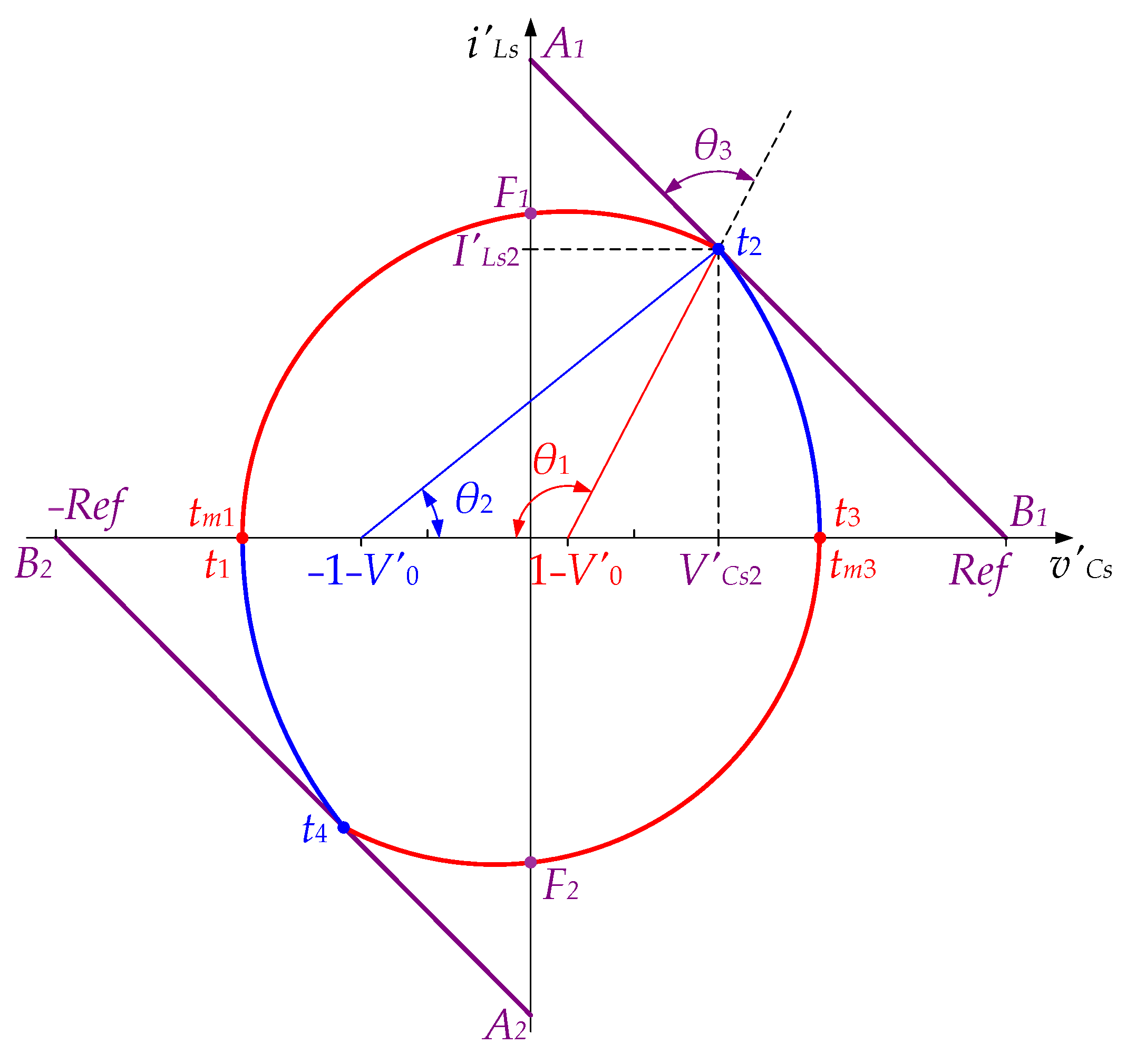
26] was based on a circuit’s behavior similar to that with optimal control of the operating trajectory. The significant simplification of the control was due to the use of a linear control law, describing a linear combination of the voltage across the capacitor and the current through the inductance in the series resonant circuit. The nature of the method is illustrated using
Figure 2, where a trajectory described by the steady-state representative point is presented.
The trajectory is composed of four arcs whose centers lie on the abscissa. The first arc has a center with coordinates (1–
V′0, 0) and angle
θ1. It corresponds to the transistors’ (
S1,
S3) conduction interval. It starts at point
t1(
V′Cs1,
I′Ls1) and ends at point
t2(
V′Cs2,
I′Ls2), respectively. Initially, the current through the series inductance is zero (
I′Ls1 = 0), and the voltage across the capacitor acquires a negative peak value (
V′Cs1 = −
V′CsM). The second arc has a center with coordinates (−1–
V′0, 0) and an angle
θ2. It corresponds to the conduction interval of the freewheeling diodes (
D2,
D4). It starts at point
t2(
V′Cs2,
I′Ls2) and ends at point
t3(
V′Cs3,
I′Ls3), respectively. Now,
I′Ls3 = 0 and
V′Cs3 =
V′CsM. The other two arcs describe the operation in the next half-period. As expected, their centers are located mirror to the ordinate. For the third arc, which corresponds to the conduction of the switches (
S2,
S4), the center has coordinates (−1 +
V′0, 0). The center of the fourth arc is given by coordinates (1 +
V′0, 0). It corresponds to the conduction interval of the freewheeling diodes (
D1,
D3). Accordingly, the first and third arcs have the same radii and angles. Analogically, the second and the fourth arcs have equal radii and angles. Therefore, the coordinates of point
t4(
V′Cs4,
I′Ls4) will be symmetric to point
t2(
V′Cs4 = −
V′Cs2,
I′Ls4 = −
I′Ls2). Furthermore, the following equation is valid for the angles of the arcs:
Obviously, the turn-on instants of the transistors are always on the abscissa because the current in the resonant circuit iLs changes its direction, and MOSFETs’ body diodes are switched off. The switching of the rectifier diodes (D5 ÷ D8) takes place at the same points. The transition of the representative point from the second to the first quadrant or from the fourth to the third quadrant is detected by the change in the sign of the variable v′Cs.
The main idea of the considered control technique is to define one control line
A1B1 (
Figure 2) in the first quadrant (and one in the third quadrant -
A2B2, respectively) in the plane specified by (7) and to turn the transistors off when the trajectory of the representative point hits these lines (points
t2 and
t4). Thus, the energy stored in the resonant tank is limited.
The equations describing the control lines are given by [
26]:
where
M is the slope of the switching lines and
Ref is the normalized control amplitude for adjusting the converter’s output power. The “−” sign in front of the
Ref parameter refers to the
A1B1 line and the “+” sign to the
A2B2 line. It is easily found that the two control lines “enclose” from the abscissa
v′Cs an area from −
Ref to +
Ref.
2.2. Simple Control Method for an LLC Resonant Converter
On the basis of the analysis presented in [
27], it can be concluded that the steady-state trajectory for an LLC resonant DC-DC converter in the continuous current mode is identical to those of the classical series resonant converter. Therefore, it is possible to apply the control technique proposed in [
26], too.
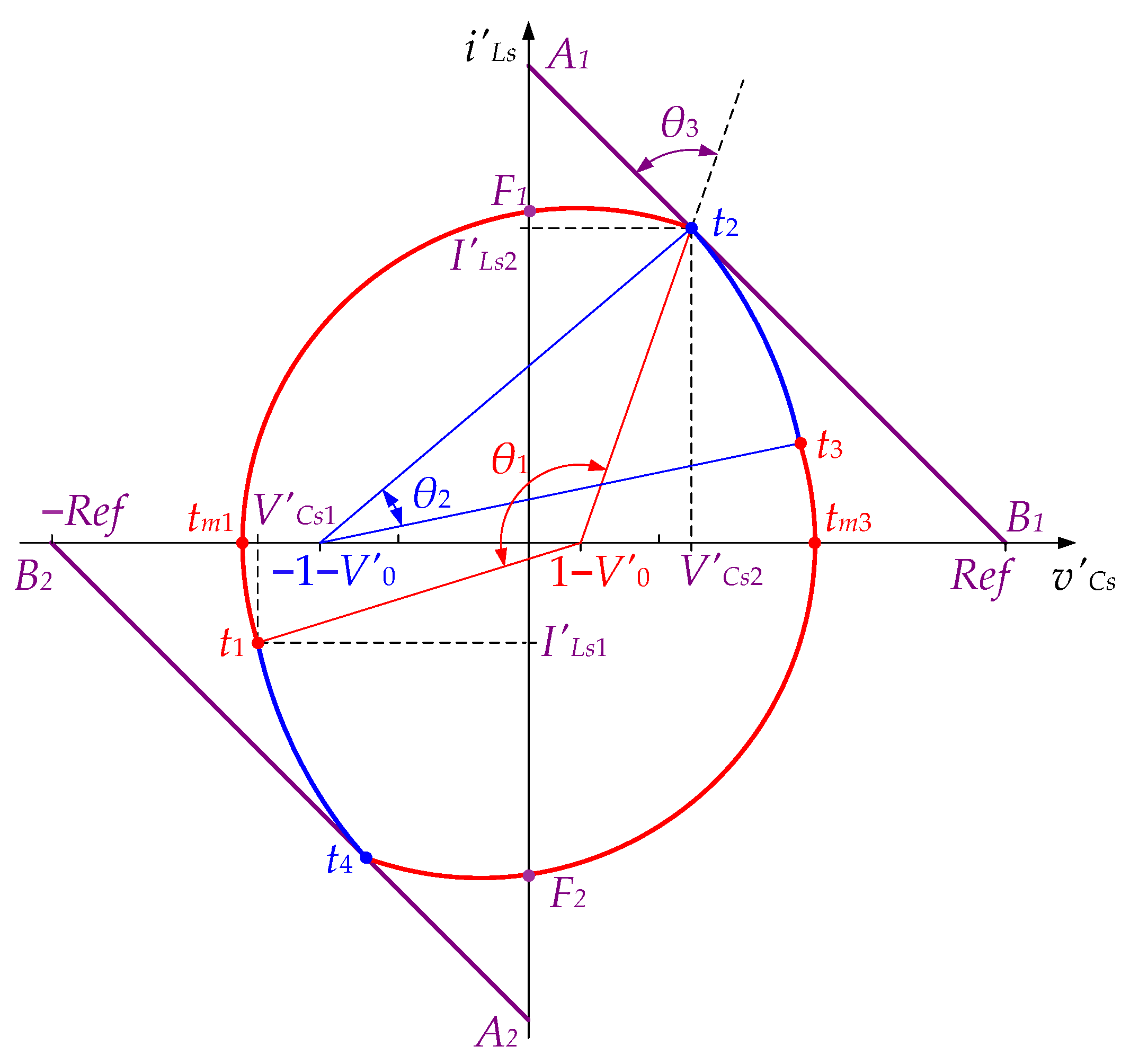
Figure 3 presents the steady-state phase plane trajectory for an LLC resonant DC-DC converter at continuous current mode (CCM).
The trajectory is also composed of four arcs whose centers have the same coordinates as in the series resonant converter. However, point
t1(
V′Cs1,
I′Ls1) is now located in the third quadrant, and point
t3(
V′Cs3,
I′Ls3) is in the first. This is due to the influence of the parallel inductance
LP. The current
iLoad (
Figure 1) passes through zero at points
t1 and
t3 when the switching of the diodes in the rectifier (
D5 ÷
D8) occurs. Nevertheless, the switching points of the transistors are always located on the abscissa, where the current in the resonant circuit
iLs changes its direction, and the freewheeling diodes stop conducting. For transistors (
S1,
S3), that takes place at point
tm1(
−V′CsM, 0), and that for
S2–
S4 at point
tm3(
V′CsM, 0), respectively. The transition of the representative point from the second to the first quadrant (point
F1) or from the fourth to the third quadrant (point
F2) is again detected by the sign change of the
V′Cs variable. Additionally, Equation (8) is valid for the angles of the arcs.
As in the case of SRC, the points, which represent the instants that correspond to the transistor’s turn-off, remain in the first quadrant—point
t2(
V′Cs2,
I′Ls2)—or the third quadrant—point
t4(
V′Cs4,
I′Ls4). Therefore, the control lines
A1B1 in the first and
A2B2 in the third quadrants (
Figure 3) in the plane defined by (7) can also be determined from (9). Thus, it is proposed that switches turn off when the trajectory of the representative point hits these lines (points
t2 and
t4) too.
2.3. Implementation of the Control Method
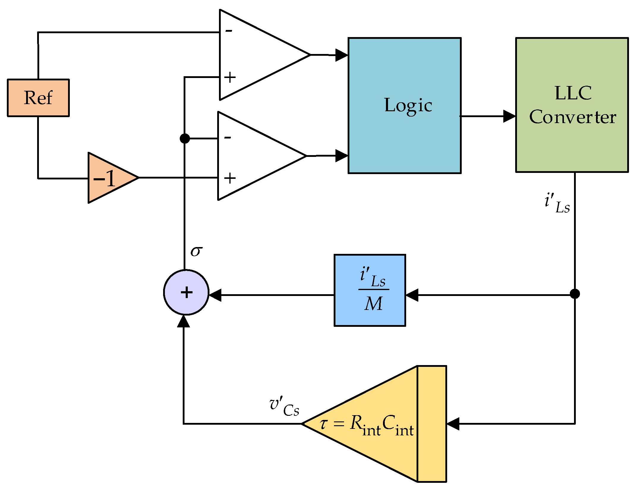
A functional block diagram, illustrating the implementation of the considered simple control method for an LLC DC-DC converter, is presented in
Figure 4. As mentioned previously, the control method is based on a linear combination of the voltage across the capacitor and the current through the inductance in the series resonant circuit.
A control variable
σ, expressed in terms of the state variables
v′Cs and
i′Ls, is used to determine the switching instant of the transistors:
The switching off in the first quadrant (point
t2) occurs at
σ = +
Ref, and that in the third quadrant (point
t4) at
σ = −
Ref. It is accomplished using the two comparators and the logic circuit (
Figure 4). Changing the value of the control parameter
Ref will change the energy stored in the resonant circuit. With respect to determining the normalized values of the state variables in [
26], it is proposed that the variable
v′Cs be determined from the current signal
i′Ls through the inductance
Ls, via a passive integrating circuit. Moreover, no precise recommendations for the design of the integrating circuit are given. Hence, the solution to this problem is obtained as follows:
The above equation shows that
v′C can be obtained based on variable
i′Ls simply via the integration circuit (
Figure 4), whose time constant
τ is defined as follows:
i.e., the time constant is reciprocal to the natural frequency of the series tank. Thus, the value of σ is uniquely determined based solely on the measurement of the current in the series resonant circuit.
In [
26], the value of the angular factor was recommended to be
M = −1.0. Thus, the normalized values of the voltage across the capacitor
Cs and the current through the inductance
Ls and their corresponding energies have an equal influence on the control.
Furthermore, the converter has the best dynamic behavior at this value of
M. In the steady state, the trajectory of the representative point reaches the control lines every half-period. At these times, the corresponding transistor pairs are turned off. By changing the value of the parameter
Ref, the resonant circuit’s energy level and the trajectory type are changed, and the output power of the converter is regulated. The transition of the representative point from the second to the first quadrant (point
F1) or from the fourth to the third quadrant (point
F2) is detected by changing the sign of the variable
v′Cs. If the trajectory does not reach a control line, the switch pair continues to conduct until the current
i′Ls becomes equal to zero (points
tm1 or
tm3). The next pair of switches starts conducting without freewheeling diodes previously conducted. Thus, the arc radii are increased during each subsequent half-period, which should result in the steady state being reached. However, as can be noticed, the proposed control can theoretically remain stable only when the following condition is satisfied:
Otherwise, the steady-state trajectory cannot reach the control lines. Hence, the converter will operate at a resonance concerning the series circuit (LS, CS). The occurrence of this “unstable” mode is determined on one side by the magnitude of the control parameter Ref and on the other side by the value of the output current I0.
3. The Characteristics of the LLC Converter
In this paragraph, the output, control and load characteristics for an LLC converter controlled by the discussed algorithm are considered. Furthermore, the influence of the inductance ratio
a on the circuit’s characteristics is discussed. An analysis of a LLC DC-DC converter using the state plane technique was presented in [
27]. The expressions for the fundamental quantities determined at steady-state operation of the LLC DC-DC converter with frequencies above the resonant frequency
ω0 of the series circuit (
LS,
CS) are given by:
Normalized output voltage:
Normalized values of the currents and voltages at point
t1(
V′Cs1,
I′Ls1) and point
t3(
V′Cs3,
I′Ls3)
Normalized values of the currents and voltages at point
t2(
V′Cs2,
I′Ls2) and point
t4(
V′Cs4,
I′Ls4)
Normalized maximum value
V′CsM of the voltage across the series capacitor
CsNormalized average value of the output current
I′0Normalized average value of the transistor current
I′SavNormalized average value of the freewheeling diode current
I′Dav
The border between the continuous current (CCM) and discontinuous current (DCM) operating modes can be defined by the expression [
28]:
The above condition is fulfilled at 0 < θ2 ≤ 0.5π/ν.
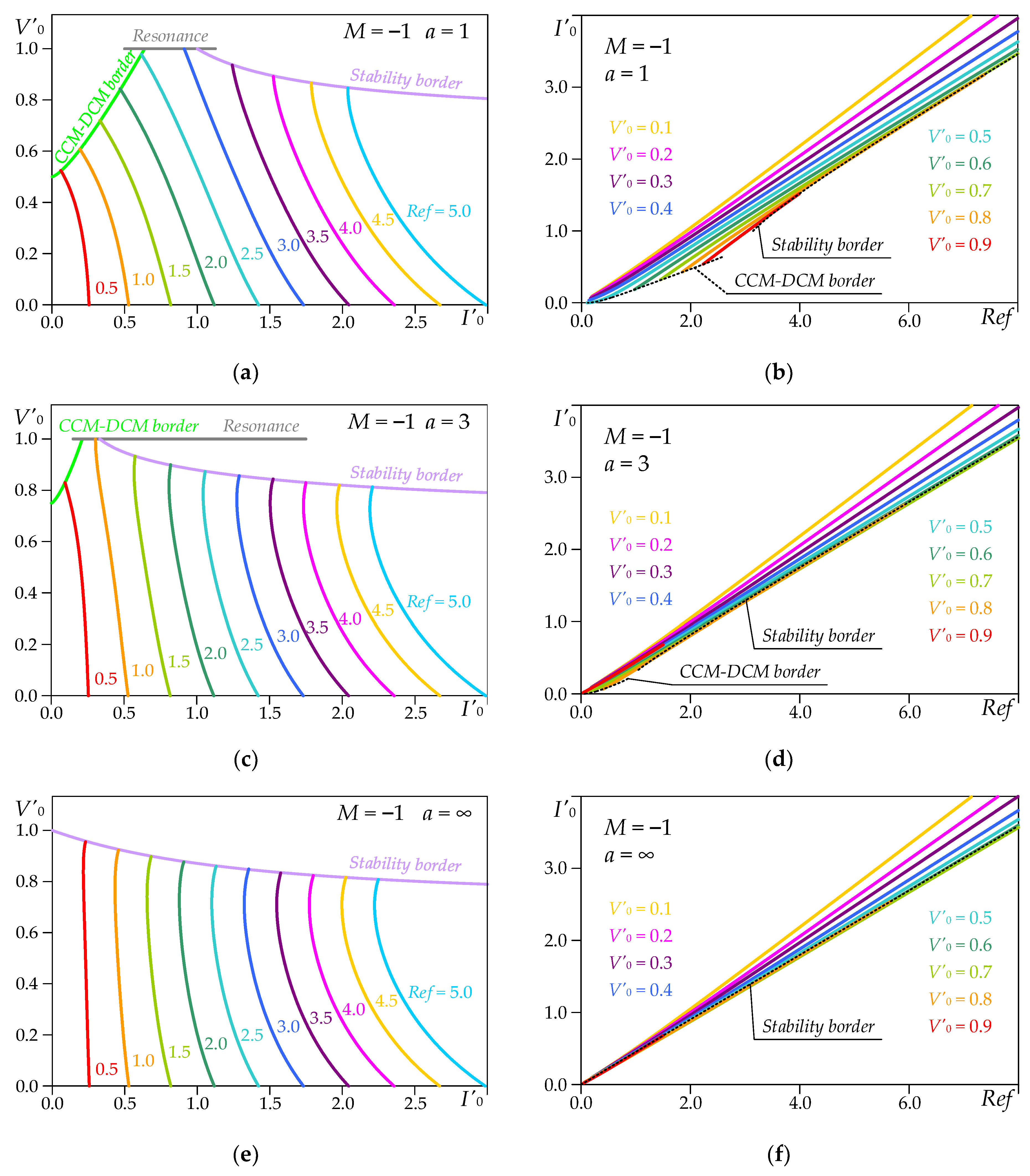
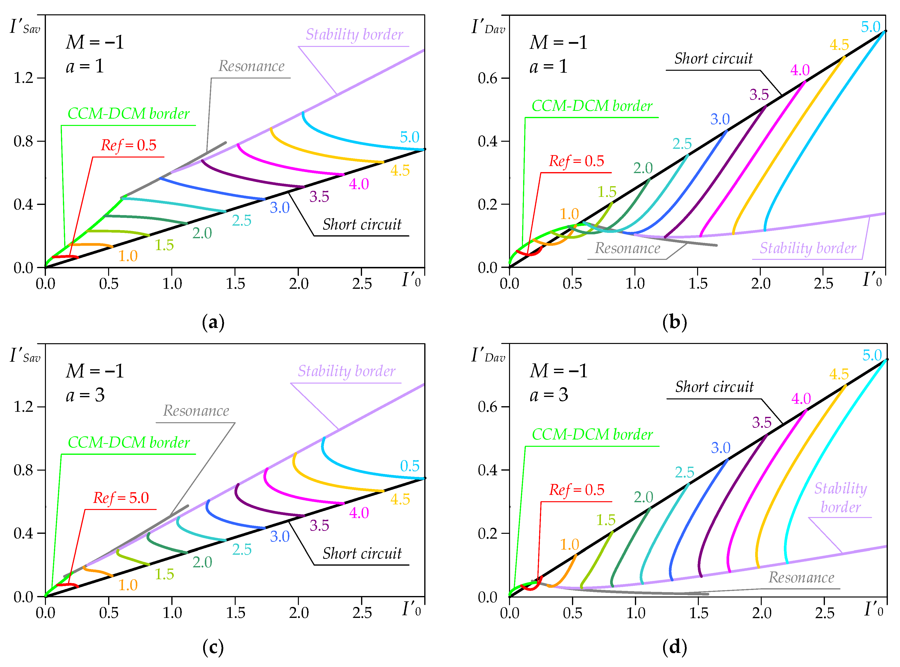
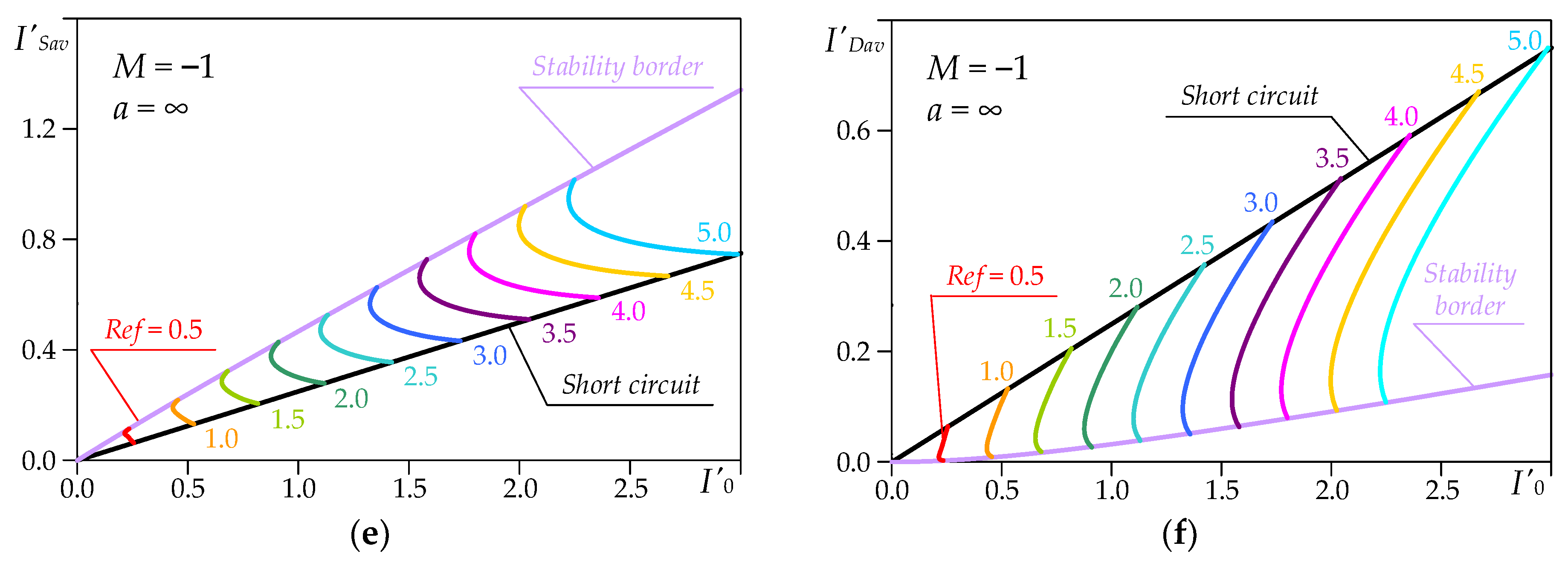
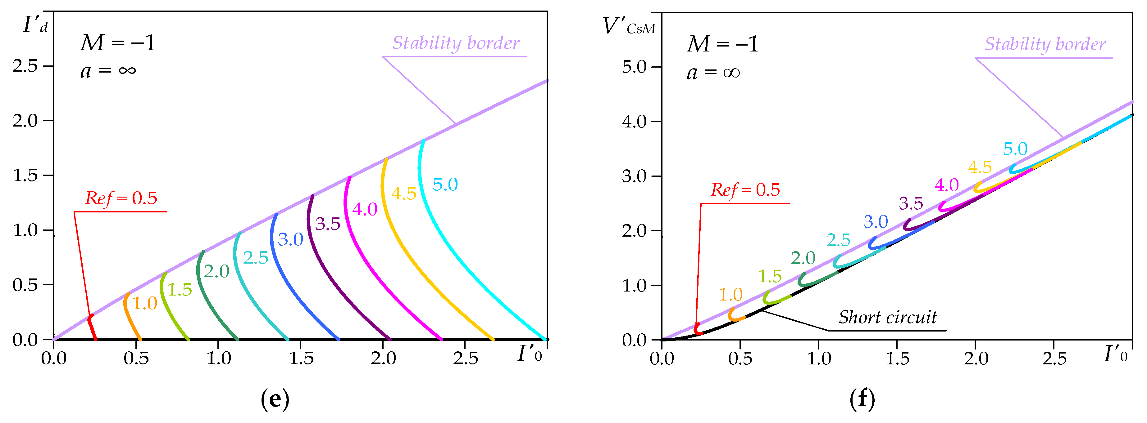
Using expressions (8), (9) and (13) ÷ (23), the relationships between the main quantities can be obtained to illustrate the properties of the resonant LLC DC-DC converter controlled by the investigated method under consideration in the continuous current mode. The main characteristics at inductance ratios a = 1, a = 3 and a = ∞ are plotted using the figures below. In the area of these dependencies, a stability border is visualized, where theoretically, for the minimum value of the output current, the trajectory of the operating point still reaches lines A1B1 and A2B2. It is determined by the condition defined by (13). Furthermore, for the cases a = 1 and a = 3, the CCM-DCM borderline (bright green) and the borderline based on the condition ν = ωS/ω0 = 1 (gray) are shown.
Figure 5 shows the output characteristics
V′0(
I′0) for values of the control parameter
Ref = 0.5 ÷ 5.0 and the control characteristics
I′0(
Ref) of the converter for values of the normalized output voltage
V′0 = 0.1 ÷ 0.9.
On the basis of the waveforms given in
Figure 5, it can be concluded that with the increase in inductance ratio
a, the area of the discontinuous current mode decreases. Nevertheless, the stability border defines a theoretical possibility that when the control parameter
Ref is varied over a wide range, the normalized output voltage reaches a relatively high value (≈0.8), which increases insignificantly when the inductance ratio
a decreases.
Furthermore, the output characteristics are nearly concentric curves, with the distance between them being apparently proportional to the change in the control parameter Ref. When a short-circuit occurs, the converter remains operational, and also the value of the output current does not depend on the inductance ratio, since the parallel inductance has no influence.
It can also be noticed that for a relatively small value of the ratio a = 3, the output characteristics are obviously not significantly different from those of the series resonant converter (a = ∞).
The control characteristics
I′0(
Ref) are apparently linear for values of the control parameter
Ref ≥ 1. This can be easily explained by the concentric placement of output characteristics. From the results presented in
Table 1, it can be reported that the dynamic coefficient Δ
I′0/Δ
Ref actually varies within a narrow range. It can be noticed that regardless of the magnitude of the inductance ratio, at low values of the normalized output voltage (
V′0 = 0.1 ÷ 0.3) the control characteristics practically coincide. In these cases, the largest variations of the dynamic coefficient are also taken into account. For high values of the normalized output voltage (
V′0 = 0.6 ÷ 0.7), the differences between the control characteristics at
a = 3 and
a =
∞ are insignificant. Those obtained at
a = 1 deviate to a more significant degree.
Figure 6 presents the basic normalized load characteristics of the converter required for its design at inductance ratios
a = 1,
a = 3 and
a = ∞ for parameter values
Ref = 0.5 ÷ 5.0. The dependences of the normalized average current through transistors
I′Sav and the normalized average current through diodes
I′Dav versus the output current
I′0 are plotted.
When a short-circuit across the converter’s output terminals occurs, the values of I′Sav and I′Dav depend only on the magnitude of the parameter Ref. However, based on the reading taken of the stability border for the same magnitude of output current I′0, they increase when decreasing the inductance ratio. This fact confirms a shortcoming of LLC converters. Namely, for the same magnitude of output current with a decreasing inductance ratio, the losses in the power devices of the inverter increase, resulting in a decrease in efficiency.
Figure 7 presents two other important normalized load characteristics obtained for inductance ratios
a = 1,
a = 3 and
a = ∞ for parameter values
Ref = 0.5 ÷ 5.0.
They are the dependences of the average value of the input current I′d(I′0) and of the peak value of the voltage across the capacitor CS of the series storage circuit V′CsM(I′0) on the output current. The characteristics I′d(I′0) demonstrate the variation in the converter output power (P′0 = I′d) by varying the parameter Ref, taking into account the influence of the inductance ratio a. It is clear that in case of a short-circuit of the converter output terminals, according to the assumptions adopted for the analysis, P′0 = 0.
However, based on the reading taken of the stability border, it was observed that when Ref was changed from 3.5 to 5.0 the output power in relative units increased by approximately 1.49 times for a = 1. Respectively, for a = 3 this increase was 1.41 times and for a = ∞ it was 1.39 times. Therefore, even for low values of the inductance ratio, the considered circuit has very similar properties to those of a series resonant converter.
As for the other types of load characteristics, in case of a short-circuit across the output terminals, the peak value of the voltage across the capacitor CS depends only on the parameter Ref. Based on the reading taken of the stability border at Ref = 5, V′CsM= 3.295 for a = 1 and V′CsM = 3.266 for a = ∞ can be reported. The difference is obviously not significant, and even for low values of the inductance ratio, the voltage stress on the capacitor was almost the same as that for a series resonant converter.
4. Behavioral Modeling of the LLC DC-DC Converter Simple Trajectory Control Method
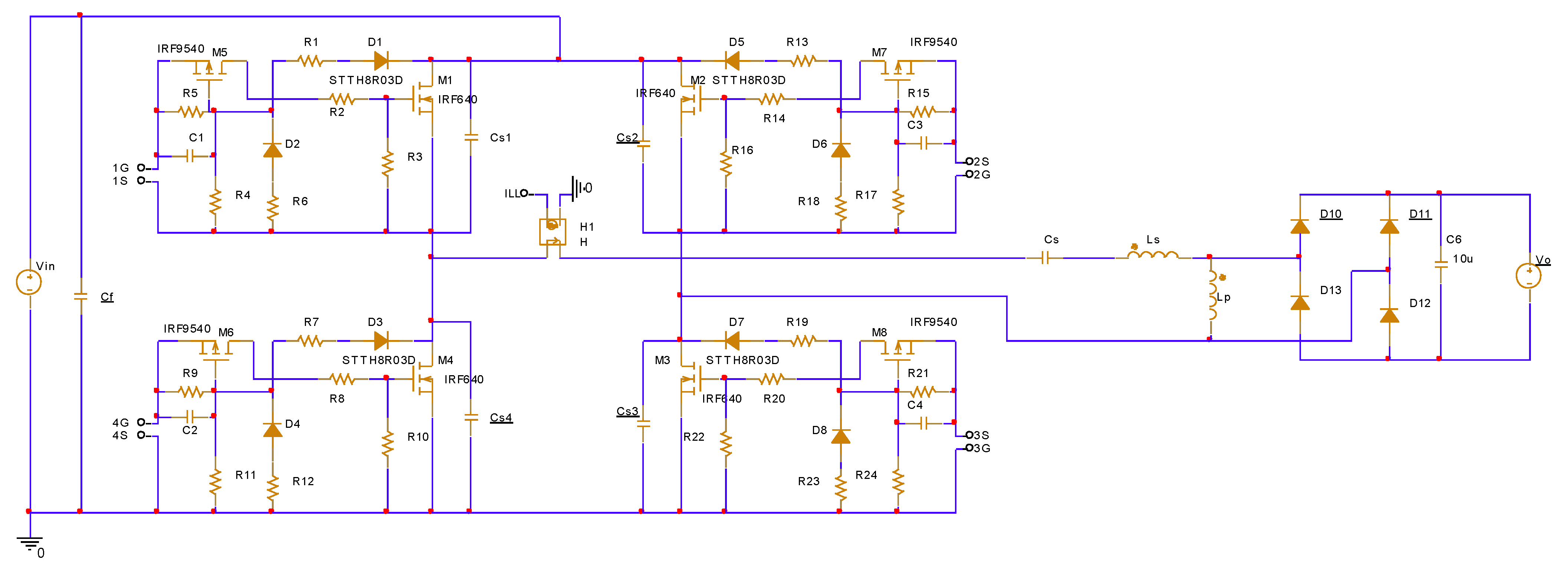
In order to verify the obtained analytical results, an LLC resonant DC-DC converter was designed with the following data: output power P = 1 kW; operating frequency fS = 50 kHz; supply voltage Vin = 200 V; output voltage V0 = 100 V. For the nominal operating mode, the frequency ratio was selected to be ωS/ω0 = 1.15. For the resonant circuit’s elements, the following values were obtained: Cs = 88.56 nF; Ls = 151.306 μH; an inductance ratio a = 3. The used MOSFET was IRF640, rectifier diodes were STTH1502D, the snubber capacitors’ values were CS1 ÷ CS4 = 1 nF and the output capacitor was C0 = 10 μF.
Figure 8 shows a simulation model of the investigated converter in the
PSpice for TI environment [
29,
30]. The output includes a voltage source
V0 which simulates the connection of a battery. Each of the transistors M1 ÷ M4 was controlled by a ZVS driver with variable dead time [
31] to be able to provide soft switching conditions over a wide load range. Through a current-controlled voltage source H1, signal ILL was obtained for the current through the resonant circuit.
The converter’s control system was described by the use of Analog Behavioral Modeling (ABM) embedded in a
PSpice for TI simulator [
29,
30]. Thus, on the one hand, sufficiently accurate results were achieved and, on the other hand, the simulation process was simplified.
The driving pulses of transistors M1 ÷ M4 were controlled by a trigger circuit whose model is shown in
Figure 9. In steady-state mode, the control pulses were fed to the driver circuits by the dependent voltage sources E1 ÷ E4. The duration of the shaped pulses was equal to one half-period. Following the considered control technique, the trigger circuit changed its state in the following cases:
- -
when the state trajectory (
Figure 3) hit a control line (points
t2 or
t4), but not before the voltage sign changed (points
F1 or
F2);
- -
the state trajectory did not hit a control line when the current’s sign changed (points tm1 or tm3).
For these reasons, the following signals were applied to the trigger circuit: input B—turn-off in the first quadrant (along the trailing edge); input C—turn-off in the third quadrant (along the trailing edge); input D—voltage sign
v′C, input E—current sign
i′L. The signals at inputs D and E were inverted. They had low levels (logic zero) at positive values of the variables
v′Cs and
i′Ls. The proposed trigger circuit was simplified and contained fewer elements than the one presented in [
26], yet fulfilled the same functions. The input signals for the trigger circuit were formed based on the current signal ILL and the control parameter
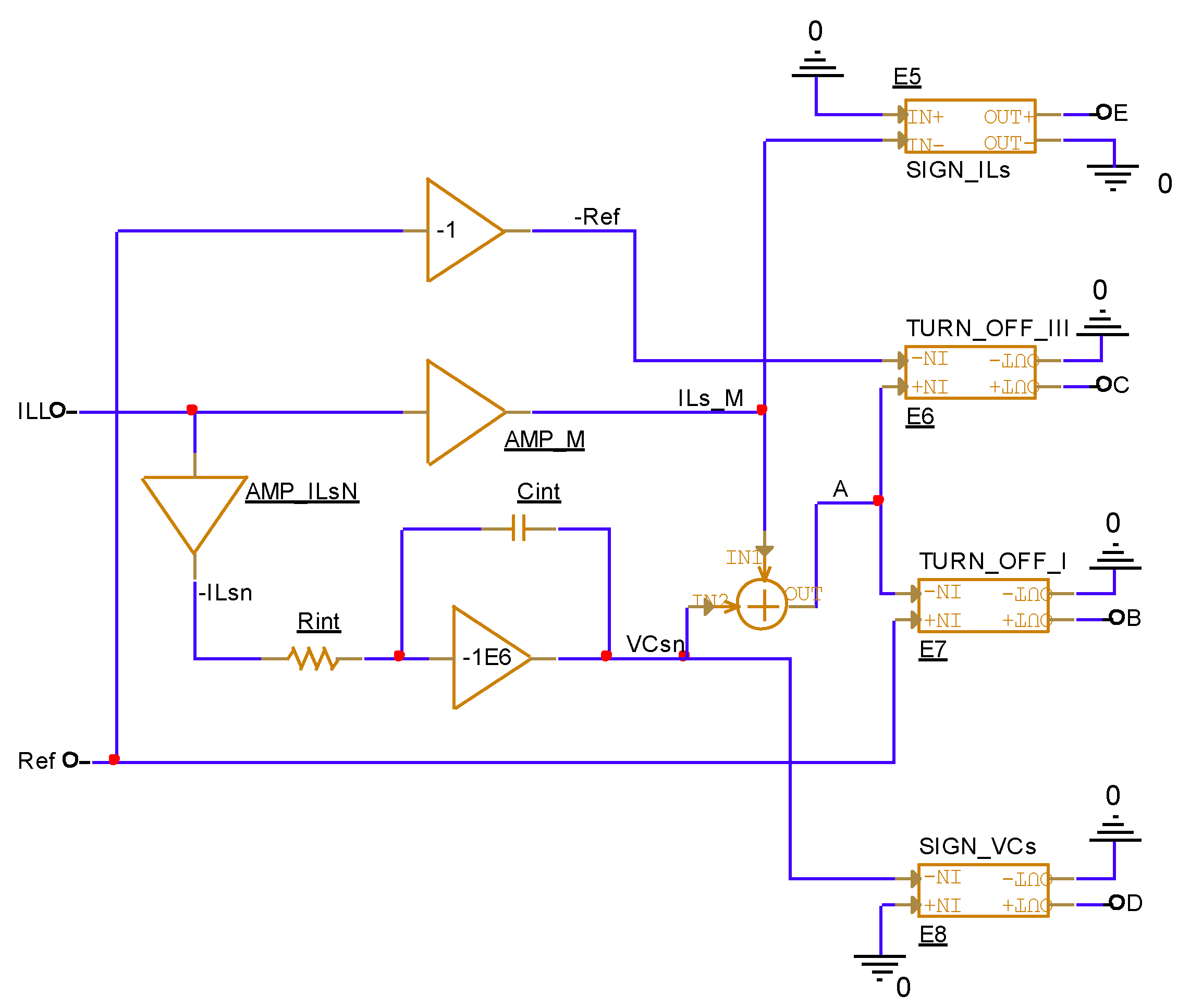
Ref using a control circuit whose analog behavior model (ABM) is shown in
Figure 10.
An inverted signal for the variable i′Ls was obtained via the AMP_ILsn amplifier. The second amplifier AMP_M formed the signal −i′Ls/M (ILs_M). Following Equation (11), an integrating amplifier formed a signal for v′Cs (VCsn). A signal for the variable σ (A) was obtained by summing in the SUM block the signals VCsn and ILs_M according to (10).
Comparison blocks SIGN_ILs, TURN_OFF_III, TURN_OFF_I and SIGN_VCs forming the logic signals (E5 ÷ E8) applied to the inputs of the trigger circuit. Their gain coefficients were defined by expressions (7) and (10). The values of elements Rint and Cint were chosen to satisfy Equation (12). They were implemented by voltage-controlled voltage sources E5 ÷ E8, which describe the function:
An advantage of the proposed control circuit was in using easy-to-tune amplifier circuits to form the control variables.
5. Simulation Results
5.1. Steady-State Simulation Results
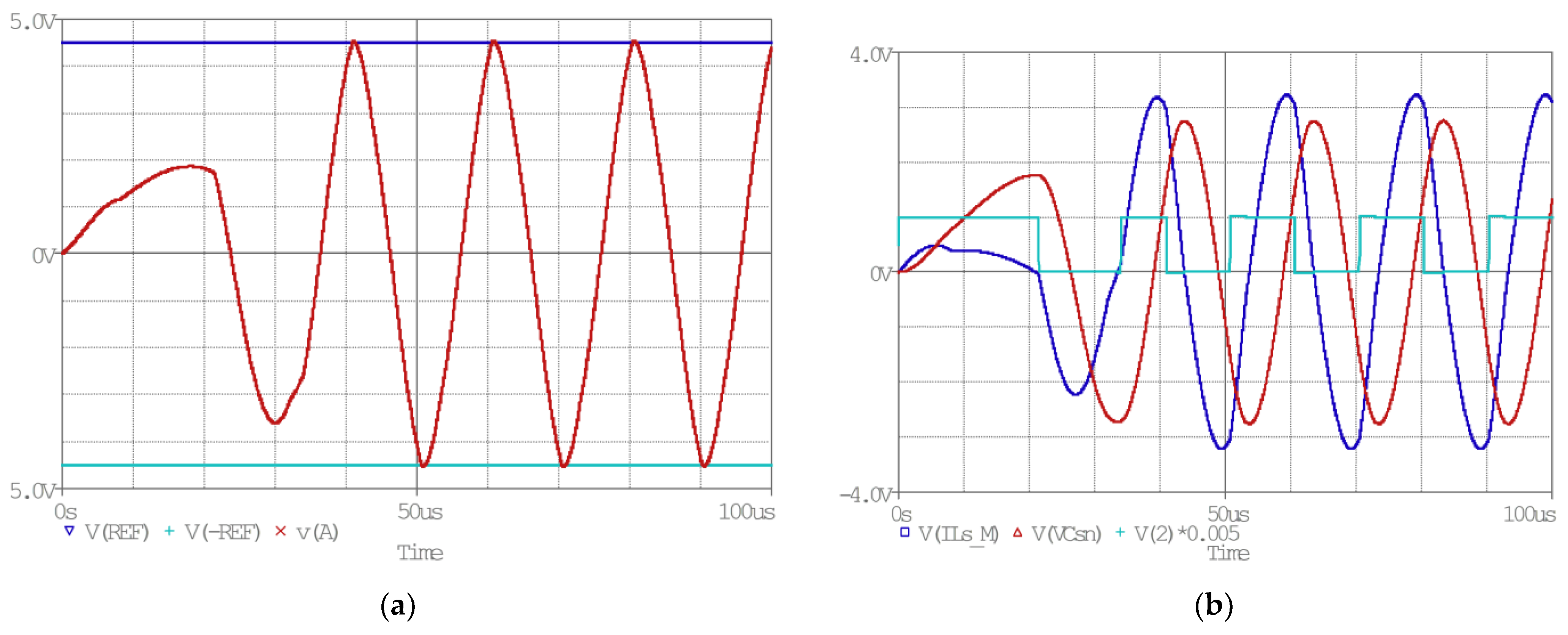
Simulation waveforms of the operation of the control circuit in steady-state mode are illustrated in
Figure 11.
Figure 11a shows the shaping of the control pulses for the given pair of transistors (
S1,
S3), which ended at positive values of the state variables (v(E) = 0 and v(D) = 0). At this point, the variable σ became greater than the control parameter
Ref (V(A) > V(REF)) and the trailing edge of the signal applied to input B of the trigger circuit was formed (V(B) = 0)—as shown in
Figure 11b. Thus, a change in the state of the trigger circuit occurred.
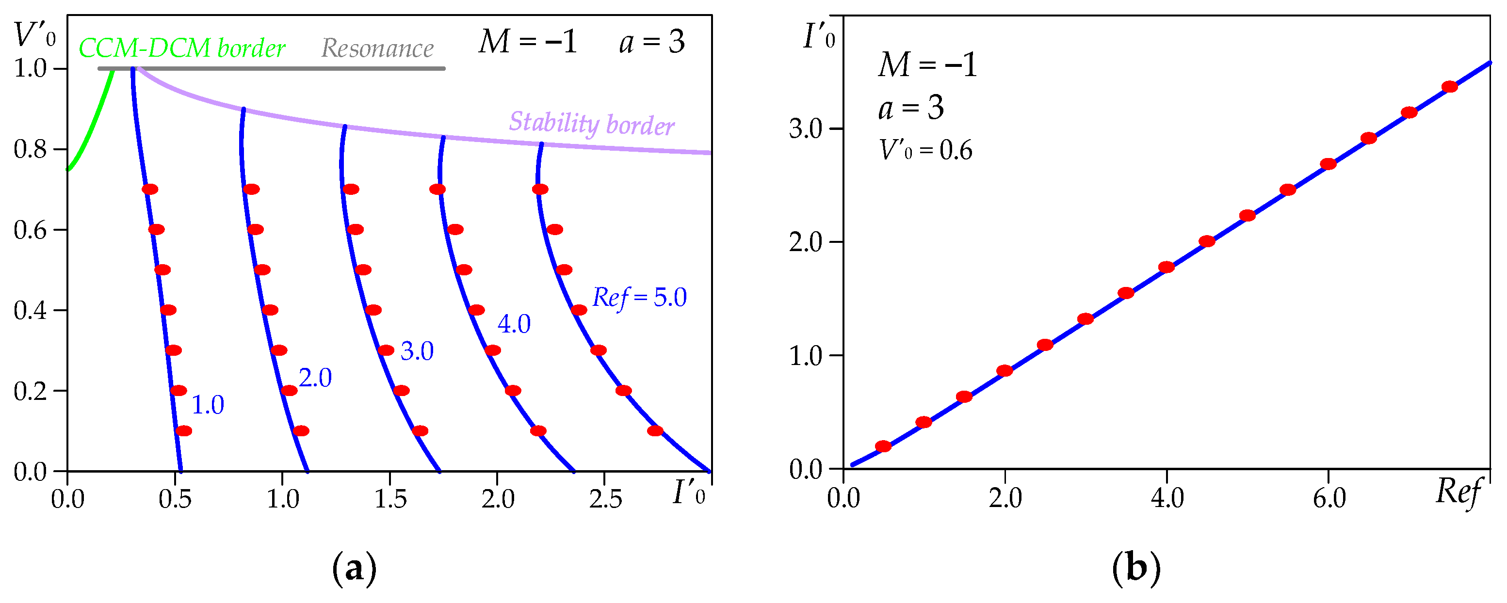
The output characteristics
V′0(
I′0) obtained on the basis of expressions (8), (9), (13) ÷ (18) and (20) were verified for several values of the control parameter
Ref = 1 ÷ 5 (
M = −1 and
a = 3). The theoretical results and those received from computer simulations were compared. The corresponding results are summarized in
Table 2.
The deviations were usually within 2%. More significant differences (around 3%) were observed for small values of the control parameter Ref.
Similarly, a control characteristic
I′0(
Ref) obtained for
V′0 = 0.6 (the nominal normalized value of the output voltage) was verified for several values of the control parameter
Ref = 0.5 ÷ 7.5 (
M = −1 and
a = 3). The corresponding results are summarized in
Table 3.
The deviations between theoretical and simulation results did not exceed 2%. Larger differences were observed for small values of the control parameter Ref. A growing tendency of the relative error was observed as zero was approached.
Figure 12a shows a graphical representation of the results from
Table 2 using dots (in red) in the area of output characteristics
V′0(
I′0) and
Figure 12b illustrates a graphical representation of the results from
Table 3 using dots (in red) in the area of the control characteristics
I′0(
Ref).
The differences demonstrated in
Figure 12 can be explained by the assumptions made for the needs of the theoretical analysis.
5.2. Dynamic Response Simulation Results
The simulation waveforms shown in
Figure 13 illustrate the converter’s behavior at start-up for induction ratio
a = 3.
In this case, due to the significant value of the control parameter Ref, the state trajectory did not reach a control line for some time interval. Moreover, the controlled switches conducted an entire half-period as the inverter voltage and current across the inductance Ls (VILs_M) were in phase. The converter operated at a frequency equal to the resonant ω0.
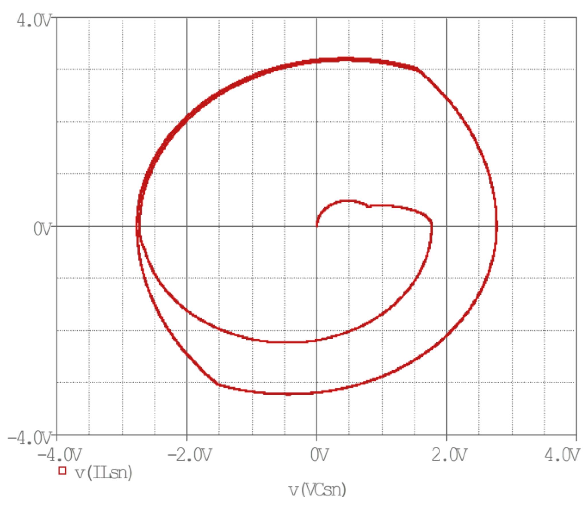
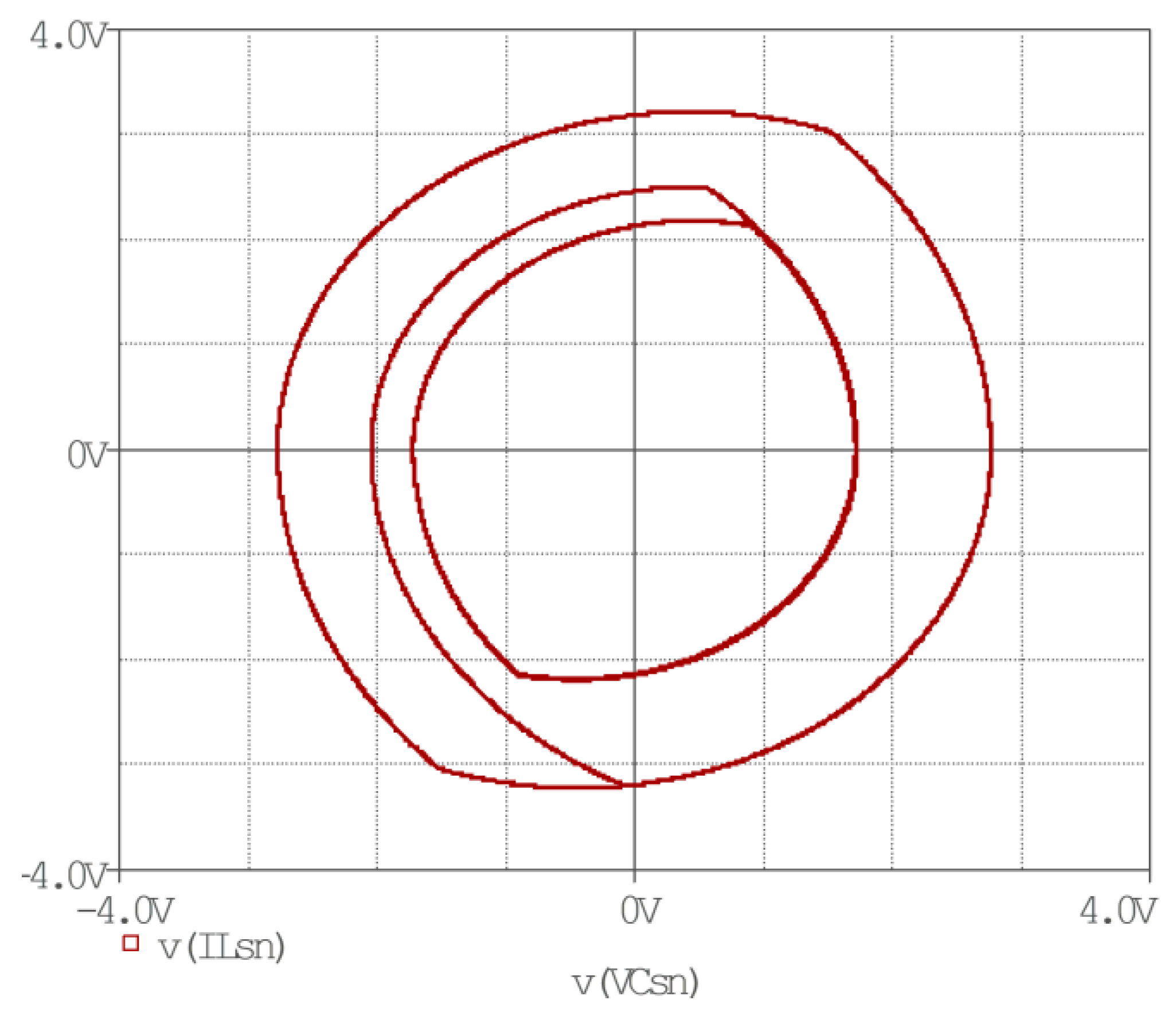
Figure 14 shows the simulation results in the phase plane when the converter is started at a control parameter
Ref = 4.5.
The dynamic response of the converter in the case of a significant increase or decrease in the control parameter
Ref is demonstrated by the state trajectories in
Figure 15 and
Figure 16, respectively.
Figure 15 illustrates that as the control parameter
Ref increased (from
Ref = 3 to
Ref = 4.5), the energy in the resonant circuit was built up by the series conduction of the transistors. It is known from the [
22] that the rate at which the tank energy can change within half a cycle is limited. The new steady state takes place for more than a half-cycle.
Similarly,
Figure 16 shows the circuit’s response when the control parameter
Ref decreased (from
Ref = 4.5 to
Ref = 3). Thus, the resonant circuit’s energy was reduced by conductions of freewheeling diodes.
The results presented in the two figures (
Figure 15 and
Figure 16) show that in both cases, the system reached the new target trajectory in the minimum time, determined only by the inherent properties of the converter. Thus, the proposed simplified control technique fully utilized the potential of the simple optimal trajectory control method for fast converter response according to the load requirements.
The performed studies through the model confirm that the considered control technique provides a fast dynamic response and stable converter operation even when the control parameter changes abruptly.
The dynamic performance of the investigated simple control method under short-circuit is shown in
Figure 17.
Within a short time, the system abruptly reached another target trajectory. The phase representation shows that the new energy level was not much greater than the previous steady-state level. Thus, the assertion that the converter had a behavior of current source stable at short-circuit mode was proven.
6. Conclusions
The application of a simple control method for a resonant LLC DC-DC converter based on a linear combination of the voltage across the capacitor and the current through the inductance in the series resonant circuit was discussed. Furthermore, the power transistors switched at zero voltage. The performed theoretical analysis showed that the converter’s control provided linear regulation characteristics and behaved like a stable current source at a short-circuit and the output current’s value did not depend on the inductance ratio, thus confirming that the behaviors of the LLC resonant converter were similar to those of the optimal trajectory control but using simpler implementation.
The boundaries, at which the simple trajectory control method was valid, were defined. The stability border on the output characteristics outlined a theoretical possibility whereby the normalized output voltage achieved a relatively high value (≈0.8) as the control parameter Ref varied considerably. Moreover, this voltage increased insignificantly when the inductance ratio decreased. The area of the discontinuous current mode increased when decreasing the value of inductance ratio a.
The control characteristics I′0(Ref) were near linear for values of the control parameter Ref ≥ 1. On the basis of the tabular results for the values of the dynamic gain ΔI′0/ΔRef, it can be concluded that at low values of the normalized output voltage (V′0= 0.1÷0.3) the control characteristics practically coincide, regardless of the magnitude of the inductance ratio. For high values of the normalized output voltage (V′0 = 0.6÷0.7), the differences between the control characteristics at inductance ratios a = 3 and a = ∞ were insignificant (0.01–0.02), whereas those obtained at inductance ratio a = 1 deviated significantly (0.04–0.08).
Regarding the dependences of the average value of the input current I′d(I′0), it was observed (the reading taken of the stability border) that when parameter Ref was changed from 3.5 to 5.0 the output power in relative units increased by approximately 1.49 times for a = 1. Respectively, for a = 3, this increase was 1.41 times and for a = ∞ it was 1.39 times. Therefore, even for low values of the inductance ratio, the considered circuit had very similar properties to those of a series resonant converter.
The properties and dynamic behavior of the converter were verified using computer simulations, both in steady state and when the control parameter was changed significantly. The proposed functional model of the control system was composed of a minimum number of elements and was easy to set up.
A comparison between theoretical and simulation results of output characteristics V′0(I′0) showed relative error within 2%. More significant differences (around 3%) were observed for small values of the control parameter Ref. Regarding the comparison between theoretical and simulation results of control characteristics I′0(Ref), it could be pointed out that the deviations between theoretical and simulation results did not exceed 2%. For small values of the control parameter Ref, greater disparities were observed. A growing tendency of the relative error was observed as zero was approached.
Additionally, calculating the value of the voltage applied to the capacitor of the series resonant circuit would be very convenient when applying the considered control method to some half-bridge circuits. Moreover, using only one measurement is a prerequisite for increasing the reliability of the proposed solution. The performed studies using the model confirm that the simplified control technique provides a fast dynamic response and robust operation when the control parameter is changed. Therefore, the converter can be successfully used as a battery-charging device.

