Article

Partial Photoluminescence Imaging for Inspection of Photovoltaic Cells: Artificial LED Excitation and Sunlight Excitation

by
Alberto Redondo Plaza
1,
Victor Ndeti Ngungu
2,
Sara Gallardo Saavedra
1,
José Ignacio Morales Aragonés
3,
Víctor Alonso Gómez
3,
Lilian Johanna Obregón
1 and
Luis Hernández Callejo
1,*
1
Department of Agricultural Engineering and Forestry, University of Valladolid, 42004 Soria, Spain
2
Department of Electrical, Electronic & Computer Engineering, University of Pretoria, Pretoria 0002, South Africa
3
Department of Applied Physics, University of Valladolid, 47002 Valladolid, Spain
*
Author to whom correspondence should be addressed.
Energies 2023, 16(11), 4531; https://doi.org/10.3390/en16114531
Submission received: 21 April 2023 / Revised: 15 May 2023 / Accepted: 31 May 2023 / Published: 5 June 2023
(This article belongs to the Section A2: Solar Energy and Photovoltaic Systems)

Abstract

:
Photovoltaic power is a crucial renewable energy source that has the potential to enhance a city’s sustainability. However, in order to identify the various issues that may occur during the lifespan of a photovoltaic module, solar module inspection techniques are crucial. One valuable technique that is commonly used is luminescence, which captures silicon emissions. This article focuses on a specific luminescence technique called partial photoluminescence. This technique involves illuminating a specific portion of the solar cell surface and recording the luminescence emission generated in the remaining area. This method has been trialed in a laboratory environment, utilizing infrared LEDs as the excitation source. An analysis of the main parameters that affect the technique is provided, where pictures have been taken under varying exposure times ranging from 50 ms to 400 ms, irradiance levels ranging from 200 W/m2 to 1000 W/m2, and a percentage of illuminated cells ranging from 10% to 40%. Furthermore, the experimental device has been modified to generate images utilizing sunlight as the excitation source. Several pictures of damaged cells were taken under an irradiance range of 340 W/m2 to 470 W/m2. The quality of the partial photoluminescence images is comparable to conventional electroluminescence images, but longer exposure times are required.

1. Introduction

Since the early 21st century, the number of individuals living in urban areas across the globe has notably increased. It is estimated that by 2050, more than 2.5 billion individuals will inhabit cities [1]. This upsurge in urbanization will result in several sustainability-related obstacles, primarily in regard to energy consumption. The integration of renewable energy solutions into urban areas has the potential to enhance energy self-sufficiency and decrease greenhouse gas emissions, thereby transforming urban regions into sustainable, autonomous communities. To accomplish sustainable urban development, cities worldwide are successfully adopting renewable energy sources to substitute for energy derived from fossil fuels.
Solar energy has become one of the most appealing alternatives to help cities attain net zero emissions, among various renewable technologies [2]. The appeal of solar energy in urban areas can be attributed to its low cost, simple installation process, and vast potential. In fact, photovoltaics integrated into cities can potentially fulfill a significant portion of a city’s electricity requirements, producing more than 60% of urban electrical demands [1].
A key objective of solar energy research and development is to continuously decrease costs and make solar energy competitive with fossil fuels. As a result, maintenance is a critical component of solar energy [3]. Commonly used inspection and characterization method for photovoltaic field inspections include visual examinations, current–voltage curve tests, thermography inspection, and luminescence pictures [4]. These methods can identify various issues that arise during the service life of the solar module. Current–voltage measurements are a useful and widely used technique that allows for a quantitative analysis of the solar module’s electrical performance. However, this test typically requires the disconnection of the photovoltaic modules, resulting in a relatively low throughput. Imaging techniques, such as infrared thermography or luminescence, are also useful for fault detection and have the potential to be integrated into unmanned aerial vehicles (UAVs) [5], making inspections economically affordable due to their high throughput.
Luminescence imaging is a technique used to characterize and inspect silicon samples, which is the primary material used in manufacturing most commercial photovoltaic cells. This technique captures electromagnetic radiation via silicon, generating images that provide insightful data regarding the solar cell performance. Luminescence images can reveal faults that do not affect the electrical or thermal performance of the module, and therefore cannot be detected by current–voltage measurements or thermography images [6]. Luminescence imaging is a valuable technique for detecting faults in photovoltaic modules including finger failures, potential induced degradation (PID), short-circuit or open-circuit faults in bypass diodes, mechanical load-induced damages, moisture corrosion, shunt faults, series resistance faults, and cracks or microcracks. [4]. Furthermore, recent approaches have shown the ability of luminescence imaging to quantitatively analyze solar cells and modules, such as determining the operational voltage of each solar cell in a module [7] or extracting parameters, such as series resistance or shunt resistance, for current–voltage curve reconstruction and power loss estimation [8,9].
Luminescence emission can be generated in a photovoltaic device (solar cell or module) through current injection (electroluminescence) or optical stimulation using a suitable light source (photoluminescence). In addition, the luminescence signal exhibits a peak emission at 1150 nm, which is a wavelength that can be detected using two types of sensors: Charged Coupled Devices (CCDs) and Complementary Metal Oxide Semiconductors (CMOS) [10].
A major drawback of electroluminescence (EL) and photoluminescence (PL) techniques is that the luminescence signal is considerably weaker than the intensity of solar radiation, which can make it difficult to capture clear images in high-irradiance conditions. As a result, luminescence images have traditionally been captured indoors or at night, which poses operational and safety issues. Furthermore, conventional luminescence techniques require a power supply for current injection into the PV array. Table 1 provides a summary of new approaches aimed at improving the conventional technique. Many of the techniques that enable high-irradiance characterization use a lock-in technique [11,12,13,14,15,16,17]. The lock-in technique involves acquiring image pairs while the PV module is in two different operating points where luminescence emission is high and null, respectively. An image subtraction is then performed to remove the background signal. In addition, some techniques use sunlight as the excitation source for PL image acquisition, eliminating the necessity of relying on an external energy source, such as a power supply.
Non-homogeneous lighting techniques are an alternative possibility in luminescence imaging, where only a portion of the solar cell surface is exposed to light [22,23,24]. PL images obtained through this technique may exhibit variations from PL images with uniform illumination due to the appearance of lateral currents in partially illuminated areas [25]. The presence of these lateral currents, the spatial arrangement of the solar cell and the percentage of lighted and captured area should be considered when interpreting non-homogeneously illuminated PL images. Line scan imaging [22,23], a type of non-homogeneous lighting technique, is especially useful in detecting series resistance defects or broken fingers, being more precise than conventional luminescence techniques. Manufacturers use line scan pictures for module fault detection and characterization. This imaging technique involves a line scan camera with a single line of pixels for the sensor and a line for the illumination source for excitation. PL line scan imaging offers a notable benefit by eliminating the requirement for electrical contacts, which can increase complexity, risk of mechanical damage, and negatively impact production throughput.
The present paper describes a technique for PL images acquisition on the entire surface of a solar cell by focusing the excitation light on one region of the cell and allowing the induced voltage to spread throughout the cell via conductor structures. This technique eliminates the need for algorithms for excitation light subtraction (lock-in technique) and line scan cameras. This paper is divided into four sections, with the second section outlining the methodology and required equipment, the third section presenting the results, and the fourth section discussing the conclusion.

2. Materials and Methods

In a laboratory setting, an artificial excitation light was used to implement the current technique. To expand the experiment’s scope, modifications were carried out to enable acquiring PL images by utilizing sunlight as the excitation source. This resulted in the construction of two distinct experimental devices, an indoor device using an LED array for excitation, and an outdoor device that uses sunlight. Both devices, as shown in Figure 1, facilitate illumination of half the solar cell while the remaining portion is photographed in a dark environment.
The LED array utilized in the experiment comprises 42 infrared LEDs model OSLON SFH 4715 (Osram Opto Semiconductors GmbH, Regensburg, Germany), with a peak wavelength of 860 nm. The LED array has been pre-calibrated to establish the corresponding irradiance that the samples will receive. The Hamamatsu InGaAs camera model C12741-03 (Hamamatsu Photonics K.K., Hamamatsu, Japan) was used to capture images of the solar cells, as it offers quicker image acquisition than CCD cameras and is insensitive to visible wavelengths and excitation light, thereby minimizing background signals. The camera has a sensor that provides a resolution of 640 × 512 pixels and a 14-bit digital output. The camera is placed at 15 cm from the samples, resulting in a resolution close to 1000 pixels/cm2. Its high resolution allows for the detection of various types of damage in the cells, ranging from major issues, such as large cracks or inactive areas, to minor failures, such as micro cracks or faulty fingers. The tested solar cells were polycrystalline silicon cells (IM156B4), with a short-circuit current of 8.99 A and an open-circuit voltage of 0.638 V. Furthermore, the outdoor setup incorporates an electrical circuit with a switch that enables altering the solar cell’s state between open circuit (OC) and short circuit (SC).
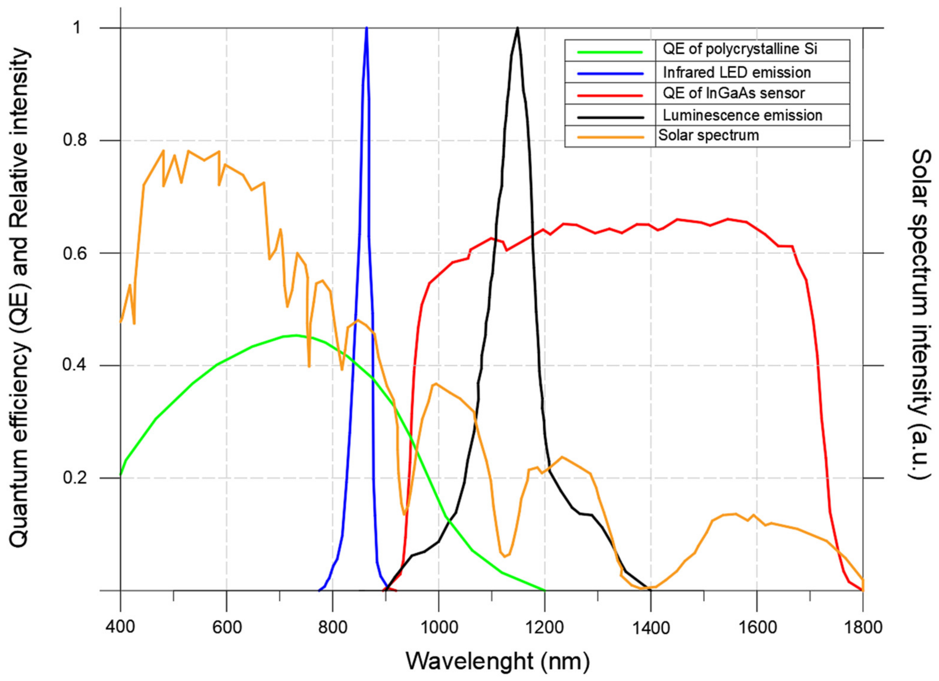
As previously stated in the introduction, the peak of the luminescence signal intensity is observed at 1150 nm, outside the visible wavelengths. To capture the luminescence emission, an InGaAs camera was utilized, which has a maximum quantum efficiency between 1000 and 1600 nm (see Figure 2). The selection of the wavelength for the lighting source is crucial as it must correspond to the solar cell’s quantum efficiency being tested. Both the emission from the infrared LEDs and sunlight match with the polycrystalline solar cells’ quantum efficiency (see Figure 2), making it possible to observe the luminescence effect.
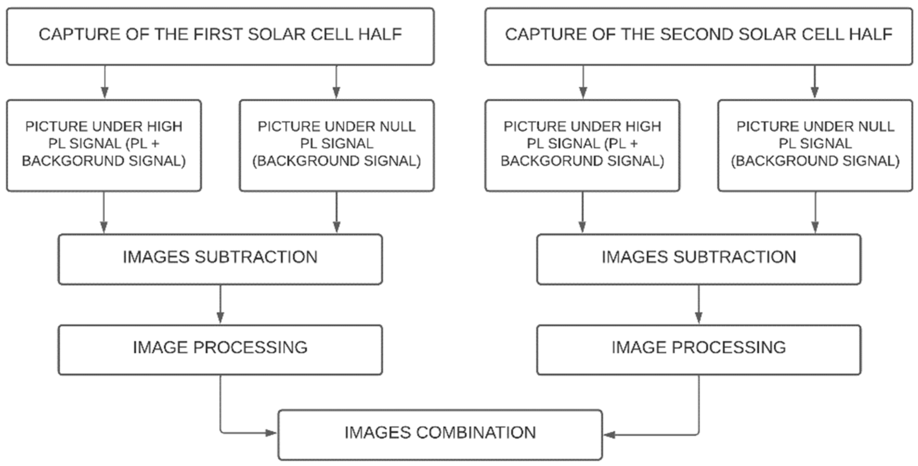
Figure 3 illustrates the schematic representation of the implemented technique’s methodology. To capture partial PL images of a solar cell, the first step is to capture the first half of the cell. This is performed by taking two pictures: one with high PL signal and another with zero PL emission. In an indoor configuration, the PL emission is zero when the LED array is off, and high when it is on. In an outdoor configuration, the PL emission is high under open circuit and zero under short circuit, as previously explained.
Next, the two pictures are subtracted by calculating the difference in intensity values for each corresponding pixel in both images. It allows to eliminate the background signal and produce a clearer picture showing only the PL emission. The resulting image is then processed to correct any optical effects generated by the camera lens, such as radial distortion, which can cause straight lines to appear curved in the picture. Here, an OpenCV algorithm has been implemented [26]. It requires a set of pictures of a chessboard taken with the same camera and lens as input. The algorithm is capable of calculating the distortion present in the pictures and applying a transformation to remove the distortion. The same steps are then repeated for the second half of the solar cell, and the two images of the halves are manually combined to obtain a full solar cell image. This step involves merging the two images and adjusting their brightness, allowing for comparison with conventional PL or EL images.
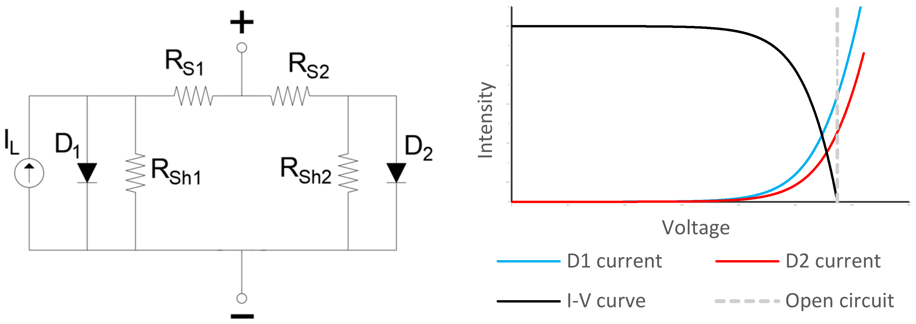
Equivalent circuit models provide a complete representation of the current–voltage (I–V) characteristics of a solar cell, module, or array under different operating conditions. The most used equivalent circuit is the one diode model [27]. Using the one diode model, simulations of the electrical performance of partially illuminated cells have been carried out. The circuit model comprises two solar cells connected in parallel, with one of them lacking a current source to simulate the unilluminated portion of the cell (see Figure 4). The current flowing through the diodes within this circuit model can be interpreted as the intensity of the PL signal, which increases exponentially with the operational solar cell voltage, as shown in Figure 4. To obtain high-quality PL images with short integration times, the solar cells were measured under open-circuit conditions to achieve maximum PL intensity emission.
Throughout the experiment, various solar cells were tested, and multiple images of the same cell were captured under different conditions. These conditions included adjustments to the exposure time, irradiance levels, and the percentage of the solar cell surface that was illuminated.

3. Results and Discussion

As mentioned above, throughout the experiment, various solar cells were tested, and multiple images of the identical solar cell were captured under various conditions, including exposure time, irradiance levels, and the proportion of the solar cell that is illuminated. From these observations, three correlations were identified.
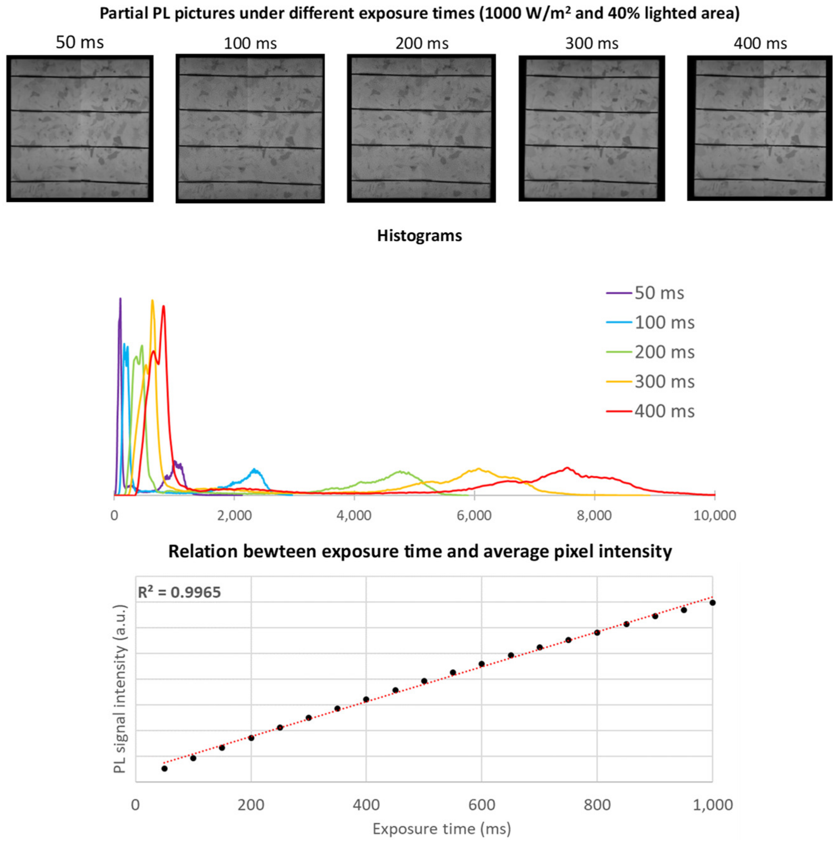
First, it should be noted that there exists a correlation between the intensity signal captured by the implemented camera and the exposure time employed. Figure 5 illustrates five images of the same solar cell with progressively increasing exposure times. All images were captured under identical irradiance conditions (1000 W/m2) and the same illuminated area (40%). Although all images exhibit sufficient quality to visualize the PL effect, differences among them can be observed by comparing their histograms. Increasing the exposure time results in a longer time during which the camera’s shutter remains open, leading to a higher intensity value. The InGaAs camera used in this study has a digital resolution of 14 bits, implying that each pixel in the images can have an intensity value ranging from 0 to 16,383. Consequently, in order to utilize the full digital resolution of the camera, it is imperative to select an exposure time that yields a signal peak around the mid-range values of the camera. Additionally, the relationship between the exposure time and the average pixel intensity has been depicted in Figure 5. A clear linear correlation between these two parameters has been observed.
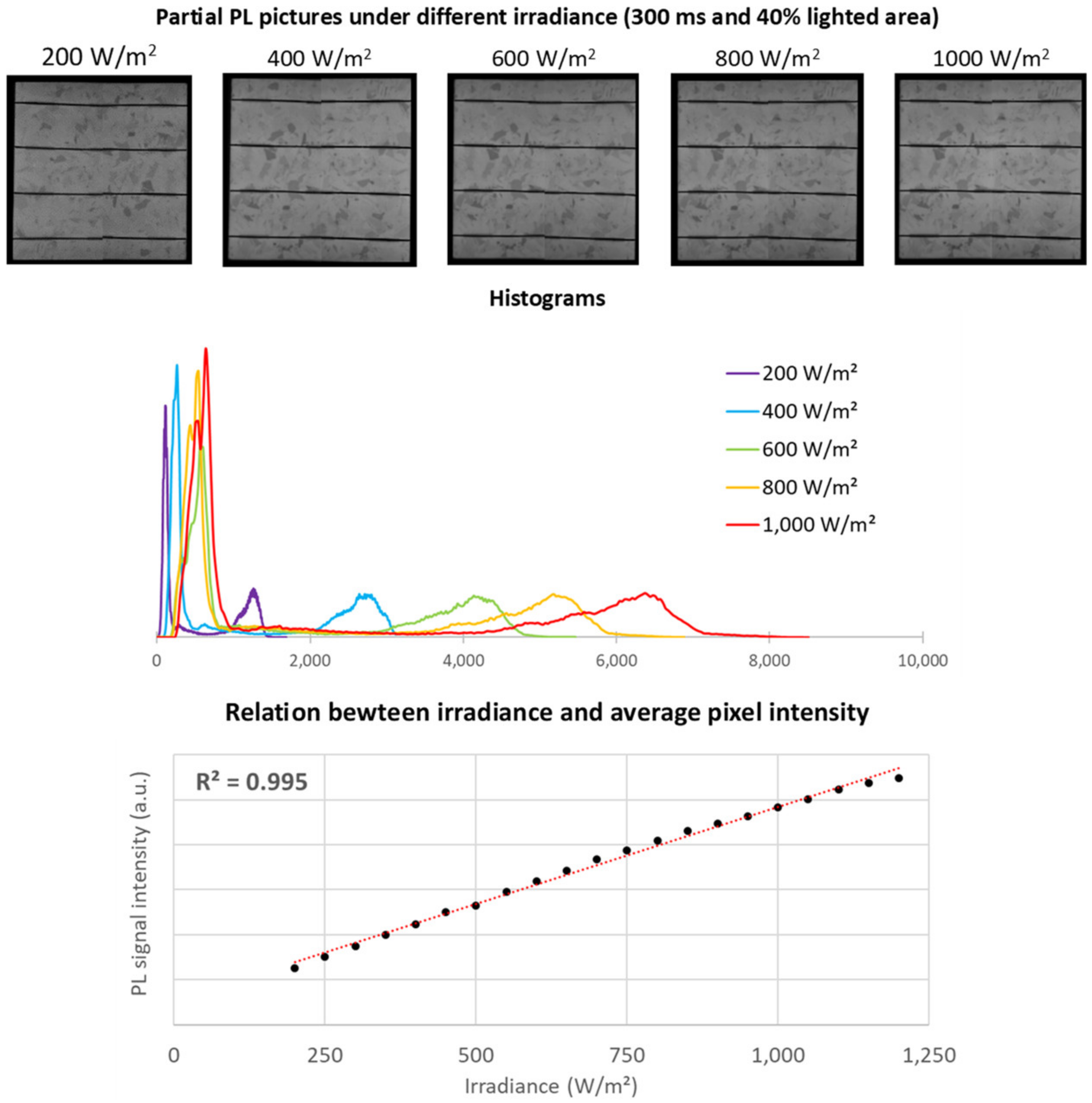
In addition, an investigation of the same solar cell under varying irradiance conditions was conducted. Figure 6 showcases five images of the identical solar cell captured using the same exposure time (300 ms) and illuminated area (40%). The images were obtained at irradiance levels ranging from 200 W/m2 to 1000 W/m2, with increments of 200 W/m2. All images exhibit commendable quality, enabling the detection of defects in the solar cells. Variations among images captured under different irradiance levels can be discerned by analyzing their respective histograms. Each histogram displays two intensity peaks: the lower peak corresponds to the dark areas (areas outside the solar cell or the cell bus bars), while the higher peak corresponds to PL signal emanating from the active surface of the solar cell. Increasing the exposure time results in a higher PL signal and a peak with greater intensity values. Furthermore, a linear correlation between the irradiance and the average pixel intensity has been observed (see Figure 6).
Lastly, an experimental investigation was carried out on the same solar cell, resulting in varying illuminated area. Figure 7 presents three images of the solar cell captured under identical irradiance conditions (1000 W/m2) and exposure time (300 ms). However, the images differ in terms of the illuminated area: 10%, 25%, and 40% of the cell’s total area. All images exhibit satisfactory quality, although their histograms differ due to the influence of the illuminated area on the PL emission within the captured region. Specifically, an increase in the lighted area results in a higher PL emission. The correlation between the average pixel intensity and the percentage of the illuminated cell area is illustrated in Figure 7, revealing a linear relationship between these two parameters.
While the idea of illuminating precisely one half of the solar cell surface and capturing the PL emission on the remaining half may appear to be an ideal approach since it maximizes the PL signal intensity, challenges arise in the overlapping region of both images due to the excitation light passing through the opaque sheet, which can mask potential faults in the central region of the solar cell. Therefore, it is recommended to reduce the percentage of lighted area and increase the portion that will be captured, even though it may reduce the PL signal intensity. The optimal configuration is where 40% of the solar cell surface is illuminated, and the remaining 60% is captured by the InGaAs camera.
In summary, it is possible to acquire high-quality partial PL pictures under different irradiance conditions and proportions of illuminated area. However, it is necessary to set up an exposure time in the camera leading to a histogram with a PL peak in the middle-range values of the camera, which means that the entire digital resolution of the camera is being used. These images demonstrate the potential of partial PL in detecting and characterizing faults in solar cells.
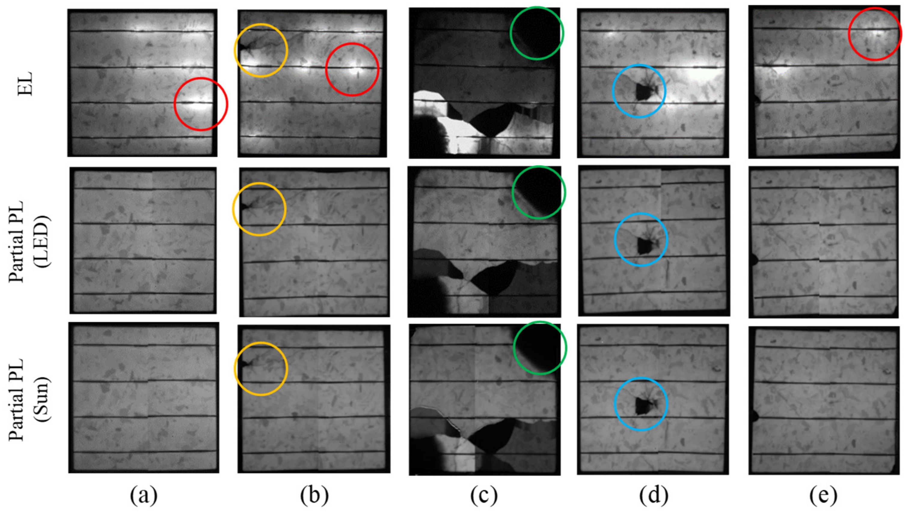
Partial PL images, similar to conventional EL images, are effective in detecting various types of faults in solar cells. Figure 8 presents the luminescence pictures of five different solar cells. The first row displays a conventional EL image captured at 8 A current and 50 ms exposure time. The second row displays the partial PL images using the infrared LED array as the excitation source. The equivalent irradiance supplied by the LED array is 1000 W/m2, while the exposure time used is 200 ms. Finally, the third row provides the partial PL images captured using sunlight as the excitation source. The images were taken under an irradiance range of 340 to 470 W/m2 and an exposure time of 300 ms.
Both EL images and partial PL images provide valuable information regarding the performance and condition of solar cells. Partial PL is capable of detecting inactive areas, cracks, and various types of faults that are also identifiable in conventional EL images. Certain defects, such as cracks (indicated by yellow circles), inactive areas (indicated by green circles), or inactive areas resulting from cracks (indicated by blue circles), are clearly visible in both the imaging techniques.
However, there are notable differences between conventional EL and partial PL images. Conventional EL images may exhibit bright spots (indicated by red circles) that are not present in partial PL images. These bright spots correspond to regions with high current density within the solar cell. As PL images are obtained through optical excitation, this particular effect is not captured. Consequently, conventional EL imaging is more suitable for analyzing the electrical performance of the solar cell, while partial PL images provide additional insights into the quality of the silicon structure.
It is worth highlighting that there is no significant difference between images acquired using an LED array as the excitation source and those where the PL signal is induced by sunlight. Both methods yield comparable results, indicating the effectiveness of partial PL imaging under different excitation conditions.
This study primarily focuses on demonstrating the capability of the method to identify qualitative defects in solar devices. However, it is important to note that analyzing quantitative parameters (such as series resistance mapping or study the lifetime of minority carriers) using this technique requires additional considerations that may differ from conventional EL or PL images. Factors, such as the effect of lateral currents or the relative position of the cell, can influence the interpretation of quantitative data.

4. Conclusions

This study demonstrates the feasibility of acquiring PL images by illuminating a solar cell area while capturing the PL emission from the remaining area in a dark environment. The proposed technique has been successfully implemented in indoor conditions using an infrared LED array as the excitation source. Furthermore, the experiment has also been conducted outdoor using sunlight as the excitation source. The key benefit of this method is that it eliminates the need for a lock-in technique to remove the background signal, which simplifies the process and reduces the acquisition time. However, partial PL images require a longer exposure time than conventional EL images and involve capturing and combining two pictures. While partial PL pictures require an exposure time of around 200–300 ms, conventional EL pictures only need 50 ms of exposure to achieve a similar digital resolution. Despite this, the quality of the partial PL images is similar to that of conventional EL images, indicating that the partial PL method is an efficient tool for finding solar cell defects.
Several experiments were conducted, and it was found that the optimal setup for the solar cell involves illuminating 40% of the surface and capturing the PL emission in the remaining 60%. This approach ensures that the area that the excitation light affects is removed and the emission of the PL signal is maximized, thereby reducing the exposure time. The partial PL technique has been shown to produce high-quality images across several irradiance conditions, ranging from 250 to 1000 W/m2 and percentage of lighted area, ranging from 10% to 40%. Moreover, this method has been modified for field measurements where sunlight is used as the excitation source. This provides two benefits: first, it enables the acquisition of luminescence images in daylight without requiring the use of background signal removal techniques; and second, unlike traditional EL and PL imaging techniques that rely on sources of external energy, such as power supply or uniform lighting devices, partial PL can generate images using sunlight. The pictures taken using sunlight as the excitation source were captured within an irradiance range of 340 W/m2 to 470 W/m2. These images exhibit similar results to the ones obtained using the LED array.
However, one significant drawback of this method is the manual combination process, which is time-consuming. Therefore, future efforts will be aimed at automating the combination process to increase efficiency and achieve an approach with a speed comparable to other techniques, such as line scan PL. To achieve this goal, it is crucial to design the process correctly to prevent an increase in computational costs compared to traditional EL techniques.

Author Contributions

Conceptualization, L.H.C. and V.A.G.; methodology, A.R.P. and V.A.G.; investigation, A.R.P.; software, V.A.G.; validation, A.R.P. and V.N.N.; Writing—Original draft, A.R.P.; Writing—Review and editing, V.N.N., S.G.S., V.A.G., J.I.M.A., L.J.O. and L.H.C. All authors have read and agreed to the published version of the manuscript.

Funding

This work has been funded by the Spanish Ministry of Education through the National Program FPU (grant number FPU21/04288).

Data Availability Statement

Data sharing not applicable.

Acknowledgments

This study was supported by the Universidad de Valladolid with ERASMUS+ KA-107. We also appreciate the help of other members of our departments.

Conflicts of Interest

The authors declare no conflict of interest.

References

  1. Kammen, D.M.; Sunter, D.A. City-Integrated Renewable Energy for Urban Sustainability. Science 2016, 352, 922–928. [Google Scholar] [CrossRef] [PubMed] [Green Version]
  2. Goel, M.; Verma, V.S.; Tripathi, N.G. Solar Energy in Cities. In Solar Energy: Made Simple for a Sustainable Future; Springer Nature: Singapore, 2022; pp. 161–173. ISBN 978-9-81192-099-8. [Google Scholar]
  3. Hernández-Callejo, L.; Gallardo-Saavedra, S.; Alonso-Gómez, V. A Review of Photovoltaic Systems: Design, Operation and Maintenance. Sol. Energy 2019, 188, 426–440. [Google Scholar] [CrossRef]
  4. Köntges, M.; Kurtz, S.; Packard, C.; Jahn, U.; Berger, K.A.; Kato, K.; Friesen, T.; Liu, H.; Van Iseghem, M. Review of Failures of Photovoltaic Modules; IEA-PVPS: Paris, France, 2014. [Google Scholar]
  5. Niccolai, A.; Gandelli, A.; Grimaccia, F.; Zich, R.; Leva, S. Overview on Photovoltaic Inspections Procedure by Means of Unmanned Aerial Vehicles. In Proceedings of the 2019 IEEE Milan PowerTech, Milan, Italy, 23–27 June 2019; IEEE: New York, NY, USA, 2019; pp. 1–6. [Google Scholar]
  6. Høiaas, I.; Grujic, K.; Imenes, A.G.; Burud, I.; Olsen, E.; Belbachir, N. Inspection and Condition Monitoring of Large-Scale Photovoltaic Power Plants: A Review of Imaging Technologies. Renew. Sustain. Energy Rev. 2022, 161, 112353. [Google Scholar] [CrossRef]
  7. Potthoff, T.; Bothe, K.; Eitner, U.; Hinken, D.; Köntges, M. Detection of the Voltage Distribution in Photovoltaic Modules by Electroluminescence Imaging. Prog. Photovolt. Res. Appl. 2010, 18, 100–106. [Google Scholar] [CrossRef]
  8. Colvin, D.J.; Schneller, E.J.; Davis, K.O. Extracting Cell Level Characteristics from Photovoltaic Module Electroluminescence Images. In Proceedings of the 2019 IEEE 46th Photovoltaic Specialists Conference (PVSC), Chicago, IL, USA, 16–21 June 2019; IEEE: New York, NY, USA, 2019; pp. 2740–2742. [Google Scholar]
  9. Kropp, T.; Schubert, M.; Werner, J. Quantitative Prediction of Power Loss for Damaged Photovoltaic Modules Using Electroluminescence. Energies 2018, 11, 1172. [Google Scholar] [CrossRef] [Green Version]
  10. Ulrike, J.; Magnus, H.; Marc, K.; David, P.; Marco, P.; Ioannis, T.; Joshua, S.; Karl, B.; Samuli, R.; Roger, F.; et al. Review on Infrared and Electroluminescence Imaging for PV Field Applications; IEA-PVPS: Paris, France, 2018. [Google Scholar]
  11. Guada, M.; Moretón, Á.; Rodríguez-Conde, S.; Sánchez, L.A.; Martínez, M.; González, M.Á.; Jiménez, J.; Pérez, L.; Parra, V.; Martínez, O. Daylight Luminescence System for Silicon Solar Panels Based on a Bias Switching Method. Energy Sci. Eng. 2020, 8, 3839–3853. [Google Scholar] [CrossRef]
  12. Bhoopathy, R.; Kunz, O.; Juhl, M.; Trupke, T.; Hameiri, Z. Outdoor Photoluminescence Imaging of Photovoltaic Modules with Sunlight Excitation. Prog. Photovolt. Res. Appl. 2018, 26, 69–73. [Google Scholar] [CrossRef]
  13. Kunz, O.; Rey, G.; Juhl, M.K.; Trupke, T. High Throughput Outdoor Photoluminescence Imaging via PV String Modulation. In Proceedings of the 2021 IEEE 48th Photovoltaic Specialists Conference (PVSC), Fort Lauderdale, FL, USA, 20 June 2021; IEEE: New York, NY, USA, 2021; pp. 0346–0350. [Google Scholar]
  14. Bhoopathy, R.; Kunz, O.; Juhl, M.; Trupke, T.; Hameiri, Z. Outdoor Photoluminescence Imaging of Solar Panels by Contactless Switching: Technical Considerations and Applications. Prog. Photovolt. Res. Appl. 2020, 28, 217–228. [Google Scholar] [CrossRef]
  15. Koester, L.; Astigarraga, A.; Lindig, S.; Moser, D. Development of Daylight Photoluminescence Technique for Photovoltaic Modules and Investigation of Temperature Dependency. In Proceedings of the 37th European Photovoltaic Solar Energy Conference and Exhibition (EU PVSEC), Online. 7–11 September 2020; pp. 908–913. [Google Scholar]
  16. Vuković, M.; Høiaas, I.E.; Jakovljević, M.; Flø, A.S.; Olsen, E.; Burud, I. Outdoor Photoluminescence and Electroluminescence Imaging of Photovoltaic Silicon Modules in a String. In Proceedings of the 11th International Conference on Crystalline Silicon Photovoltaics (SILICONPV 2021), Hamelin, Germany, 19–23 April 2022; p. 030012. [Google Scholar]
  17. Kropp, T.; Berner, M.; Stoicescu, L.; Werner, J.H. Self-Sourced Daylight Electroluminescence from Photovoltaic Modules. IEEE J. Photovolt. 2017, 7, 1184–1189. [Google Scholar] [CrossRef]
  18. Coello, J.; Pérez, L.; Domínguez, F.; Navarrete, M. On-Site Quality Control of Photovoltaic Modules with the PV MOBILE LAB. In Proceedings of the Energy Procedia: 2013 ISES Solar World Congress; Elsevier: Amsterdam, The Netherlands, 2014; Volume 57, pp. 89–98. [Google Scholar]
  19. Navarrete, M.; Pérez, L.; Domínguez, F.; Castillo, G.; Gómez, R.; Martínez, M.; Coello, J.; Parra, V. On-Site Inspection of PV Modules Using an Internationally Accredited PV Mobile Lab: A Three-Years Experience Operating Worldwide. In Proceedings of the 31st European Photovoltaic Solar Energy Conference and Exhibition, Hamburg, Germany, 14–18 September 2015; pp. 1989–1991. [Google Scholar]
  20. Ballestín-Fuertes, J.; Muñoz-Cruzado-Alba, J.; Sanz-Osorio, J.F.; Hernández-Callejo, L.; Alonso-Gómez, V.; Morales-Aragones, J.I.; Gallardo-Saavedra, S.; Martínez-Sacristan, O.; Moretón-Fernández, Á. Novel Utility-Scale Photovoltaic Plant Electroluminescence Maintenance Technique by Means of Bidirectional Power Inverter Controller. Appl. Sci. 2020, 10, 3084. [Google Scholar] [CrossRef]
  21. Kunz, O.; Rey, G.; Bhoopathy, R.; Hameiri, Z.; Trupke, T. Outdoor PL Imaging of Crystalline Silicon Modules at Constant Operating Point. In Proceedings of the 2020 47th IEEE Photovoltaic Specialists Conference (PVSC), Calgary, AB, Canada, 14 June 2020; IEEE: New York, NY, USA, 2020; pp. 2140–2143. [Google Scholar]
  22. Juhl, M.; Weber, J.W.; Zafirovska, I.; Juhl, M.K.; Weber, J.W.; Kunz, O.; Trupke, T. Module Inspection Using Line Scanning Photoluminescence Imaging. In Proceedings of the 32nd European Photovoltaic Solar Energy Conference and Exhibition, Munich, Germany, 20–24 June 2016. [Google Scholar] [CrossRef]
  23. Iskra, Z.; Juhl, M.K.; Weber, J.W.; Wong, J.; Trupke, T. Detection of Finger Interruptions in Silicon Solar Cells Using Line Scan Photoluminescence Imaging. IEEE J. Photovolt. 2017, 7, 1496–1502. [Google Scholar] [CrossRef] [Green Version]
  24. National Renewable Energy Laboratory; Johnston, S. Contactless Electroluminescence Imaging for Cell and Module Characterization. In Proceedings of the 2015 IEEE 42nd Photovoltaic Specialist Conference (PVSC 2015), New Orleans, LA, USA, 14 December 2015; Institute of Electrical and Electronics Engineers Inc.: New York, NY, USA, 2015. [Google Scholar]
  25. Sulas, D.B.; Johnston, S.; Jordan, D.C. Comparison of Photovoltaic Module Luminescence Imaging Techniques: Assessing the Influence of Lateral Currents in High-Efficiency Device Structures. Sol. Energy Mater. Sol. Cells 2019, 192, 81–87. [Google Scholar] [CrossRef]
  26. OpenCV: Camera Calibration. Available online: https://docs.opencv.org/4.x/dc/dbb/tutorial_py_calibration.html (accessed on 15 May 2023).
  27. Cotfas, D.T.; Cotfas, P.A.; Kaplanis, S. Methods to Determine the Dc Parameters of Solar Cells: A Critical Review. Renew. Sustain. Energy Rev. 2013, 28, 588–596. [Google Scholar] [CrossRef]
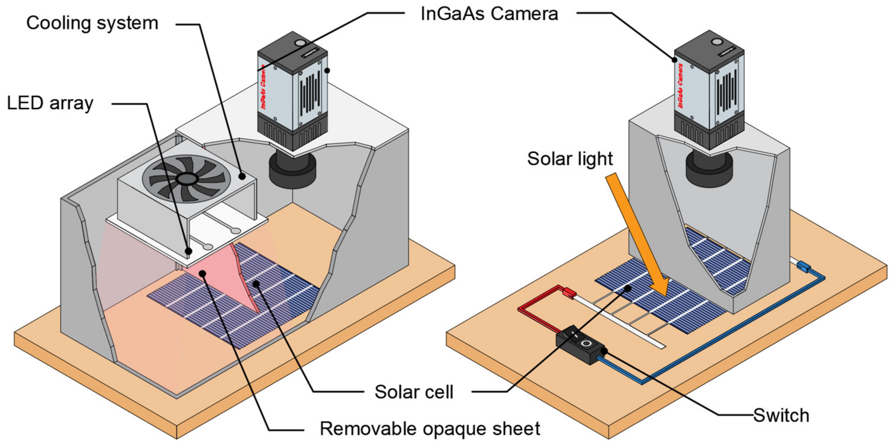
Figure 1. Experimental devices for partial PL images acquisition: indoor and outdoor configuration.
Energies 16 04531 g001
Figure 2. Quantum efficiency of the silicon solar cells and InGaAs camera, relative intensity of luminescence signal, infrared LED array relative signal intensity and solar spectrum intensity.
Energies 16 04531 g002
Figure 3. Procedure schematic for partial PL images acquisition.
Energies 16 04531 g003
Figure 4. Electrical model of a partial shaded solar cell.
Energies 16 04531 g004
Figure 5. Influence of exposure time on partial PL image acquisition.
Energies 16 04531 g005
Figure 6. Influence of irradiance on partial PL image acquisition.
Energies 16 04531 g006
Figure 7. Influence of illuminated area on partial PL image acquisition.
Energies 16 04531 g007
Figure 8. Comparison between conventional EL (8 A and 50 ms), partial PL with LED excitation (1000 W/m2 and 200 ms) and partial PL with sun excitation (340–470 W/m2 and 300 ms) of different photovoltaic cells (ae). High density current spots are marked in red circles, cracks are indicated by yellow circles, inactive areas are denoted by green circles, and inactive areas resulting from cracks are represented by blue circles.
Energies 16 04531 g008
Table 1. Summary of outdoor luminescence techniques for PV applications.
MethodEL/PLDay/NightDiscussion
Mobile
laboratory
[18,19]
ELDay/NightA truck equipped with several measuring devices allows for the full characterization of PV modules, including EL images, infrared thermography images, current–voltage measurements, and insulation testing. However, this method requires the disassembly of the PV modules.
Bidirectional
inverter
[20]
ELNightA bidirectional inverter is capable of functioning as a conventional solar inverter as well as a power supply, enabling current injection in the PV array and inducing the EL effect.
Bias switching method
[11]
EL/PLDay/NightFor daylight EL and PL imaging using lock-in technique, an electronic device is connected between the PV array and a power supply. This device allows for the injection of current for EL imaging or to shift the operating point between the open circuit (OC) and short circuit (SC) for PL imaging.
Control cell method
[12,13,14]
PLDayDaylight PL method that uses a lock-in technique to achieve a shift between two operating points: OC and Maximum Power Point (MPP), which is conducted through a control cell. If the control cell is shaded, all cells that make up the same substring will operate in OC. Conversely, if the control cell is not shaded, all cells will operate in MPP.
Inverter control method
[15,16]
PLDayDaylight PL method that uses a lock-in technique to achieve a shift between two operating points: OC and MPP, which is achieved by the solar inverter. Unlike other methods, the shift between OC and MPP is not instantaneous, taking approximately 6 s due to the Maximum Power Point Tracking (MPTT) algorithm. Therefore, a batch method is used. First, all the MPP images are captured and then the OC images are taken. This approach reduces the time required for image acquisition and also avoids the noise generated by changing irradiance conditions.
Self-sourced EL
[17]
ELDayDaylight EL method that uses a lock-in technique to image solar cells. An electronic device is used to store the energy generated by the PV modules in capacitors. After that, it boosts the voltage and injects current into the module, which leads to the EL effect.
Constant operational point PL
[21]
PLDayDaylight PL method at a constant operational point. In this approach, several images are captured using different optical filters. A main filter is used to allow the PL transmission, resulting in pictures with a high PL signal. A secondary filter is used to block the PL transmission, resulting in pictures with a low PL signal. By properly subtracting these images, the background noise can be eliminated, allowing for accurate measurements of the PL signal.
Disclaimer/Publisher’s Note: The statements, opinions and data contained in all publications are solely those of the individual author(s) and contributor(s) and not of MDPI and/or the editor(s). MDPI and/or the editor(s) disclaim responsibility for any injury to people or property resulting from any ideas, methods, instructions or products referred to in the content.