Article

A Comparative Evaluation of Wide-Bandgap Semiconductors for High-Performance Domestic Induction Heating

1
Department of Electrical Engineering, Yildiz Technical University, Istanbul 34220, Turkey
2
Department of Electrical and Electronics Engineering, Istanbul Esenyurt University, Istanbul 34510, Turkey
3
Department of Research and Development, Mamur Technology Systems Inc., Istanbul 34590, Turkey
*
Author to whom correspondence should be addressed.
Energies 2023, 16(10), 3987; https://doi.org/10.3390/en16103987
Submission received: 1 March 2023 / Revised: 17 April 2023 / Accepted: 20 April 2023 / Published: 9 May 2023
(This article belongs to the Section F3: Power Electronics)

Abstract

:
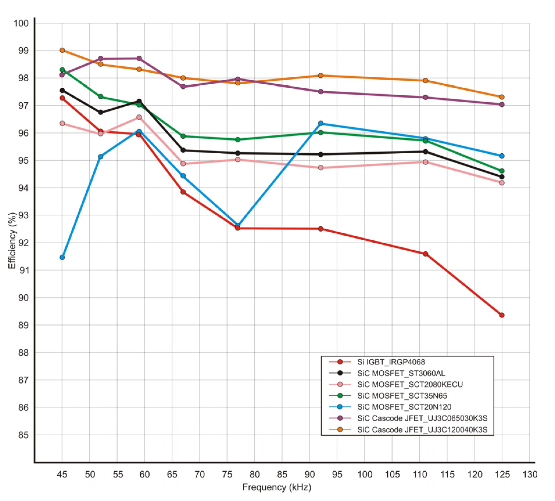
This paper presents a comparative evaluation of wide-bandgap power semiconductor devices for domestic induction heating application, which is currently a serious alternative to traditional heating techniques. In the induction heating system, the power transferred to the output depends on the equivalent resistance of the load, and the resistance depends on the operating frequency. Due to the switching characteristics of wide-bandgap power semiconductor devices, an induction heating system can be operated at higher operating frequencies. In this study, SiC and Si semiconductor devices are used in the comparison. These devices are compared according to different evaluation issues such as the turn-off energy losses, turn-off times, current fall time, the power losses of the internal diodes, and the conduction voltage drops issues. To perform the proposed evaluation, the series-resonant half-bridge inverter, which is frequently used in state-of-the-art induction heating systems, has been selected. The device suitability in an induction heating system is analyzed with the help of a test circuit. A comparison is made in terms of criteria determined by using the selected switches in the experimental circuit, which is operated in the 200 W to 1800 W power range and 45 kHz to 125 kHz switching frequency range. System efficiency is measured as 97.3% when Si IGBT is used. In the case of using SiC cascode JFET, the efficiency of the system is increased up to 99%.

1. Introduction

The semiconductor materials used in power devices determine the current and voltage values of the devices. The features expected from semiconductor power devices are low thermal resistance, wide energy bandgap, and operation at high frequencies [1]. The low thermal resistance of the semiconductor power devices results in a shorter thermal time constant.
Operating the switches at high frequencies reduces the passive component sizes and the circuit volume. The operation of the circuit at high frequencies is possible with power devices with high electron drift velocity. Power devices with wide energy bandgap have thinner layers, low internal resistance, fewer power losses, and leakage currents, so they have higher package thermal resistances and can operate at higher voltages. The Si element is often preferred in power devices because of its stable and easy production. Silicon carbide (SiC) and gallium nitrate (GaN) are materials with wide bandgap (WBG) used in semiconductor power devices [2,3].
Silicon (Si) power devices have undergone many changes from the date they were first used to the present day. In terms of maximum voltage that can be applied, operating temperature, conduction, and switching properties, these devices are getting close to their theoretically permitted limits for the materials. State-of-the-art Si-insulated gate bipolar transistors (IGBTs) have a voltage rating of five kV because of their restricted performance, and switching speeds are still slow because of tail currents. In addition, most of the commercial Si-based devices currently have a maximum junction temperature below 175 °C. The thermal limitation is due to the liquid temperature of the solder layer. The thermal performance of the device is lower than soldering when sintering or gluing is used [4]. Obtaining converters with higher power densities is difficult because of these inherent physical constraints [5].
Along with the commercial production of wide-bandgap semiconductor devices, these devices have begun to be used in state-of-the-art power converters. In contrast to Si devices, WBG devices have a large breakdown electric field, a low conduction resistance, a high switching speed, and a high junction temperature tolerance. These properties affect the conversion’s efficiency, power density, output power, and reliability [3].
As a result of the advancement in SiC technology, SiC metal-oxide field-effect transistors (MOSFETs) operating at higher powers and with better temperature strength than Si MOSFET have been produced [6]. In SiC MOSFET, the thickness of the area holding the voltage is made 10 times thinner than Si MOSFET, as shown in Figure 1, while the additive density can be increased 10 times. In this way, the on-state resistance of the SiC MOSFET decreases to one percent of the resistance of the Si MOSFET with the same properties. Thus, the on-state resistance, the main disadvantage of Si MOSFETs, is reduced. Drive circuits must include protection against the uncontrolled operation of the device caused by environmental noise [5].
JFETs have a rated voltage of 1200 V to 1700 V and a rated current of up to 48 A [7]. SiC MOSFETs are normally off power devices. In the MOSFET, the gate is insulated because there is an oxide layer between the gate and the drain. Practically no current passes from gate to source. On the other hand, generally, JFET has a reverse polarized pn junction that causes leakage current from gate to source. This causes the device to be normally on, unlike MOSFETs. Since SiC JFET is a normally on device, the negative voltage must be applied between the gate and source for the device to be off. The main disadvantage of normally on JFET is that negative voltage can cause a short circuit in the drive part of the device. For this reason, it is not preferred to be used in power electronics circuits [8].
To eliminate the disadvantage of SiC JFETs caused by the driver circuit, a SiC cascode JFET structure was created by connecting a Si MOSFET in series with the device. Here, the serial MOSFET has low conduction resistance [9,10]. This structure has the JFET’s conduction characteristics and the driving characteristics of Si MOSFET. However, due to high di/dt and dv/dt, high-frequency oscillations occur between the Si MOSFET’s parasitic capacitance and the circuit path’s leakage inductance [9]. These high-frequency oscillations can be avoided by using a snubber circuit [11]. The driving voltage of SiC cascode JFET has a wide range. Another advantage of SiC cascode JFET is that it can be used without changing the driving circuit of the Si device.
Due to their superior high efficiency, safety, cleanliness, and quick heating over conventional heating processes, domestic induction heating systems (DIHS) are becoming more and more popular on the market. In DIHS, when SiC power devices are used instead of Si, the total volume of the system decreases and power density and circuit efficiency increase [12,13,14,15,16].
The importance of efficient use of energy in terms of sustainability is increasing day by day. Therefore, it is important to increase the efficiency of domestic induction cookers, which are increasingly used in homes. The main novelty of the current study is the comparative analysis using SiC semiconductor devices, which were not compared with each other in IH systems in previous studies. Furthermore, to contribute to developing a system that operates at high frequencies with high efficiency to transmit power to nonferromagnetic metals.
The rest of the paper is structured as follows. In the “Literature Review” section, studies using WBG devices in induction heating systems were examined, and the research gap in the literature was defined. In the “Performance Parameters” section, the criteria for comparing the selected devices are given. Brief information about the general operation of the converter to be used in the device comparison and the design of the resonance tank is given in the “System Description” section. The results are given and discussed in the “Experimental Results” section. The last section, “Conclusion”, provides the concluding remarks of the present study.

2. Literature Review

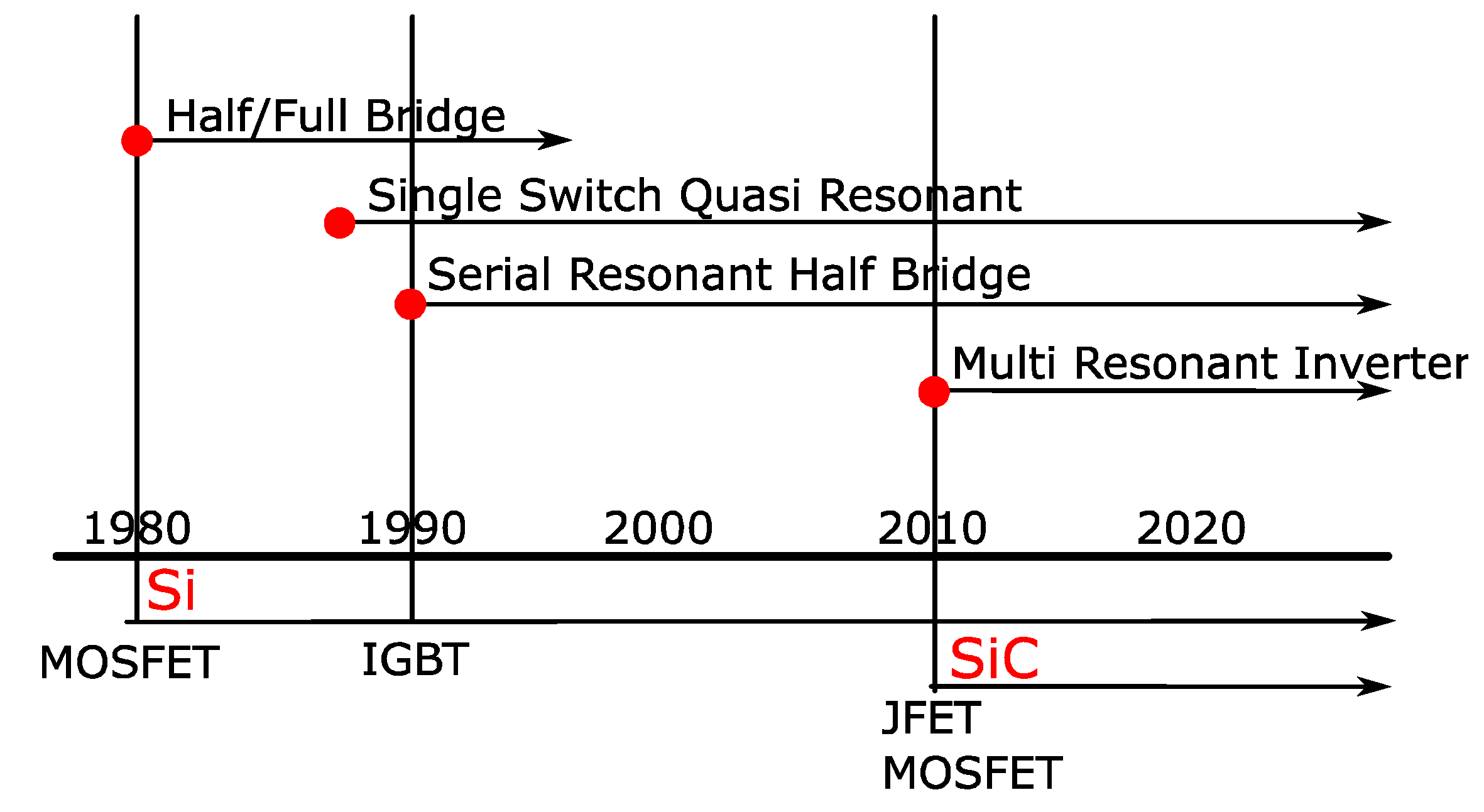
The use of IH technology in home appliances first started with MOSFET in half -bridge (HB) and full-bridge (FB) topologies. In the following years, with the discovery of the high voltage value MOSFET, the lower-cost single-switched quasi-resonant (SSQR) topology was used in home applications [12,14].
With the development of the IGBT with low conduction resistance, the efficiency of topologies has increased [17]. In IH systems, the system’s efficiency is increased by using resonance topologies in which switching power losses do not occur or are reduced [18]. In IH systems, serial resonant (SR), FB, HB, and SSQR topologies are commonly used [19,20]. Figure 2 shows the topologies and power devices used in domestic IH systems over the years. The FB topology is suitable for industrial IH systems with an output power higher than 5 kW. In domestic IH systems, low-cost SSQR topology is up to 2 kW, and HB topology is used in a cost-performance balance of up to 5 kW [21].
There are some disadvantages to SR HB topology, commonly realized with Si IGBT in DIHS [22]. These can be listed as follows:
  • Circuit volume cannot be reduced since IGBTs cannot be operated above 100 kHz;
  • Semiconductor power devices with wide bandwidth can operate at high voltages;
  • Nonferromagnetic materials cannot be heated because of the IGBT’s switching frequency, and voltage values are not high enough.
When SiC power devices are used instead of Si in IH applications, the above disadvantages are eliminated. As a result, the system’s total volume decreases and power density and circuit efficiency increase. In addition to those advantages, nonferromagnetic materials can be heated using SiC power devices [12,13,14,15,16].
Various studies have been conducted on using WBG devices in IH systems, as summarized in Table 1 [2,12,14,15,22,23,24,25,26,27,28,29,30,31,32]. In these studies, a single WBG device was mostly examined. In a limited number of studies, Si and WBG devices were examined comparatively.
Si and SiC MOSFETs were compared in FB topology used for surface hardening of irregular cylindrical parts. It has been observed that the turn-off power loss of SiC MOSFET is less than that of Si MOSFET, and the power loss of turn-on is decreased by 90% [14]. To verify the proposed multi-modulation technique in which a QR AC-AC topology was used, SiC JFET with a high voltage value was used in [12]. SiC JFET was used to achieve high performance and efficiency in the multi-output IH system realized with an FB AC-AC topology [12].
The behavior of the Si and SiC MOSFETs realized with SR FB topology has been investigated. It has been observed that the turn-off time of SiC MOSFET is 10 times lower than Si MOSFET [15]. SiC MOSFET is operated at a switching frequency of 400 kHz realized with an FB topology to separate foreign metal materials. In this case, the heatsink volume has decreased by 78% [33].
The switches’ power losses are investigated using Si IGBT, Si MOSFET, and SiC MOSFET, in which LLC topology with resonance is used. It has been observed that the lowest power loss is in SiC MOSFET [2,29]. The circuit’s efficiency and performance have been investigated using a three-phase SiC module in a new IH power supply using an interleaved resonance booster topology. The efficiencies of IH systems realized with HB and FB topologies using the SiC power module have been examined. Si IGBT module and SiC MOSFET module are used in high frequency [24]. It has been observed that the efficiency of the circuit increases with the SiC module [30]. The conduction and switching losses of SiC JFET and Si IGBT realized with a SS QR topology have been investigated [27]. SiC MOSFET is operated with FB topology at high frequency and power [25]. SiC cascode JFET is used in the domestic IH, which is realized with SR HB topology [34].
Details of the comparative studies are given in Table 2 [15,22,27,29,30]. In these studies, Si devices and SiC devices were compared in general. Although all of the studies have been examined from different aspects, the system efficiency has been examined in all except [27]. It is seen that the SiC cascode JFET, which is a combination of the superior features of the Si MOSFET and SiC JFET devices, is not compared with other devices in DIHS. As a result, the lack of comparison using the SiC cascode JFET device in the literature is seen as a research gap.
The main contribution of this work is to examine the performance of SiC cascode JFET in a DIHS using the SR HB topology and to compare it with the SiC MOSFET and Si IGBT devices used in these systems. The selected devices were compared according to the determined performance criteria. A power circuit has been created for the experimental realization. The performances of power devices in the selected 45–125 kHz switching frequency range are examined. In addition to the main contribution, this article makes four additional contributions to DIHS:
  • SiC devices that have not been compared with each other before being compared;
  • A device suitability analysis is performed using SiC power devices according to different manufacturers and voltage ratings;
  • The advantages of high switching speed SiC devices are examined;
  • A wide range and high-efficiency operation have been achieved at high frequencies, which is important for heating all metals in state-of-the-art induction heating systems.

3. Performance Parameters

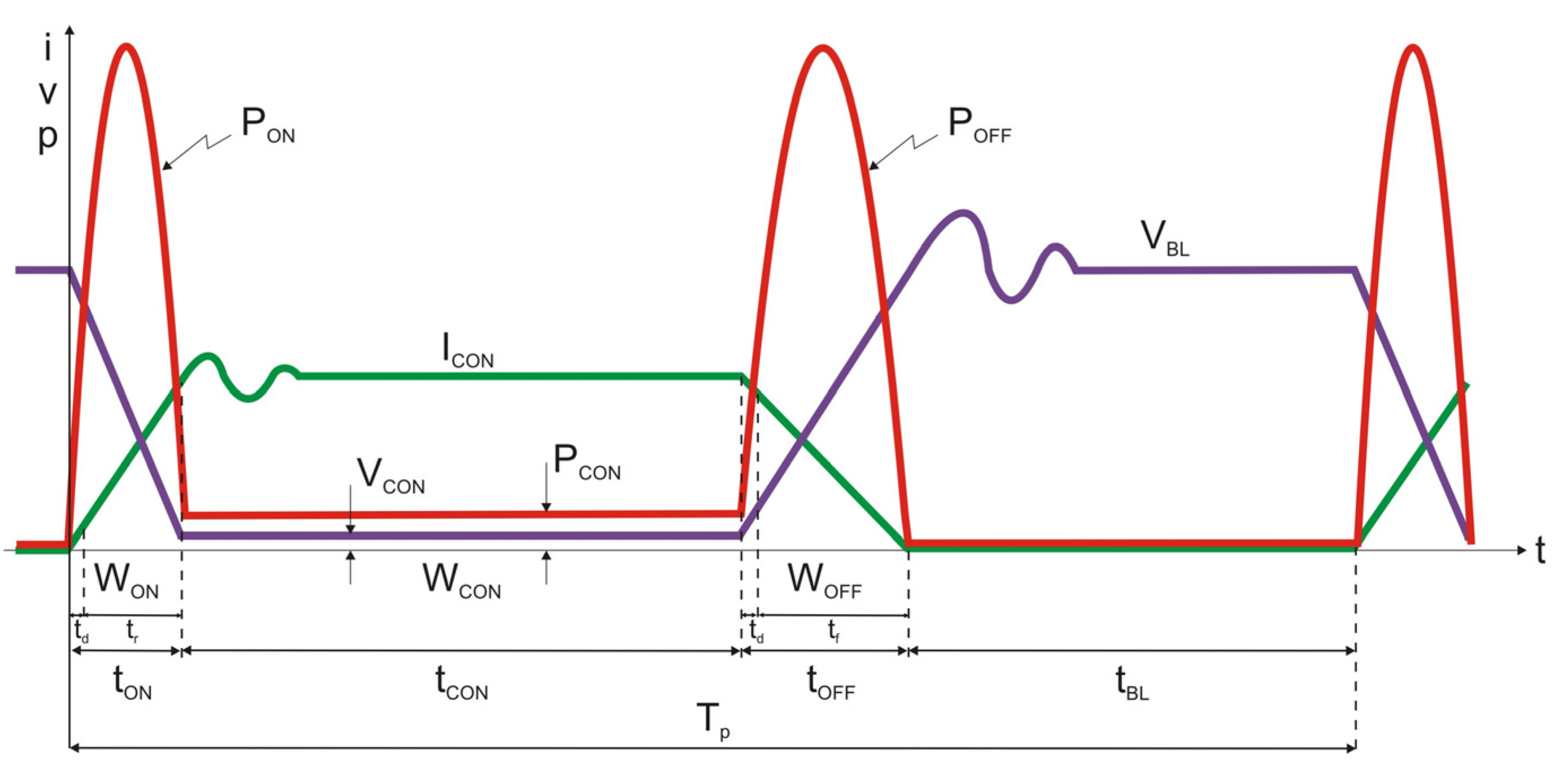
Semiconductor power devices are controlled switches that have the ability to turn on and off speedily in power electronics circuits. The voltage across the power device is low during the conduction time and high during the blocking time. There are two power losses in power devices, conduction loss and switching loss. Switching loss consists of turn-on power loss and turn-off power loss. The power devices’ current, voltage, and power loss waveforms are given in Figure 3 for one switching period [35].
The time between removing the control signal and reducing the current to 90% is called the delay time. The time that the current falls from 90% to 10% is called the falling time. The turn-off time is the sum of these times.
The power and energy losses equations are given in Equations (1)–(7). As shown in Equations (2) and (3), switching power losses are calculated by multiplying the switching frequency of the power device with the switching energy losses. Switching power losses change proportionally with the switching frequency. At high frequencies, the device can be damaged by overheating caused by the switching power loss. Therefore, choosing the suitable power device to be used at high frequency is crucial in terms of switching power loss.
The conduction losses occur depending on the conduction voltage drop or the conduction resistance of the device, as shown Equation (4). It is the primary source of power loss, especially at maximum output power. Switching and conduction losses directly affect the power converter efficiency. Therefore, these losses will be examined as the basic performance parameters in comparing the selected devices.
P C O N = 1 T p 0 t C O N V C O N i C O N
P O N = f S W E O N
P O F F = f p E O F F
P S W = P O N + P O F F
E O N = 0 t O N V O N i O N d t
E O F F = 0 t O F F V O F F i O F F d t
E s w = E O N + E O F F

4. System Description

(a)
Reference application
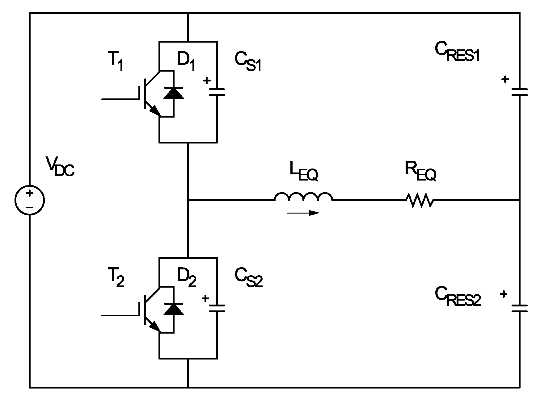
The serial resonant HB topology, which is balanced in terms of cost and performance, is frequently used in DIHS [36]. Figure 4 shows the circuit diagram of SR HB topology. In this topology, inductance current and switch voltage are in sinusoidal and square wave form, respectively. SR HB topology is usually operated above the resonant frequency in the inductive region. In the inductive region, when the freewheeling diode is in the on state, the control signal is applied to the switch. Thus, switching loss does not occur in the turn-on process of the switch. Snubber capacitors are connected in parallel with switches to reduce turn-off switching power losses. To use Si IGBTs at high frequencies, snubber capacitors must be used [37].
(b)
Resonance tank design
The equivalent series resistance REQ and inductance LEQ are used to model the IH load (inductor-pot system). A CRES resonance capacitor is used to generate series resonance with the LEQ. The equivalent resistance and inductance vary depending on the switching frequency, load materials, temperature, and alignment [38].
In the literature, there are many studies on the SR HB inverter circuit design, and different methods are used in the design process of the resonant tank [36]. One of these methods is to determine the LEQ and CRES according to the power, the minimum value of the input AC voltage (VACmin), and the selected resonance frequency (fRES) values. The input current (I) is equal to the average of the resonant current in one operating period and calculated from Equation (8).
CRES is calculated from Equation (9). By arranging the resonance frequency equation given in Equation (10), Equation (11) of the resonance inductance is obtained. The value of the resonance inductance is determined using CRES and fRES. Iteration is performed using these values, and the final values of the resonance tank are obtained. The inverter is operated above 20 kHz so that the users are not disturbed by noise while the DIHS operates [39,40].
I = 2 π P V A C m i n
C R E S = I 2 π f V A C m i n
f R E S = I 2 π L E Q C R E S
L E Q = I ( 2 π f ) 2 C R E S

5. Experimental Results

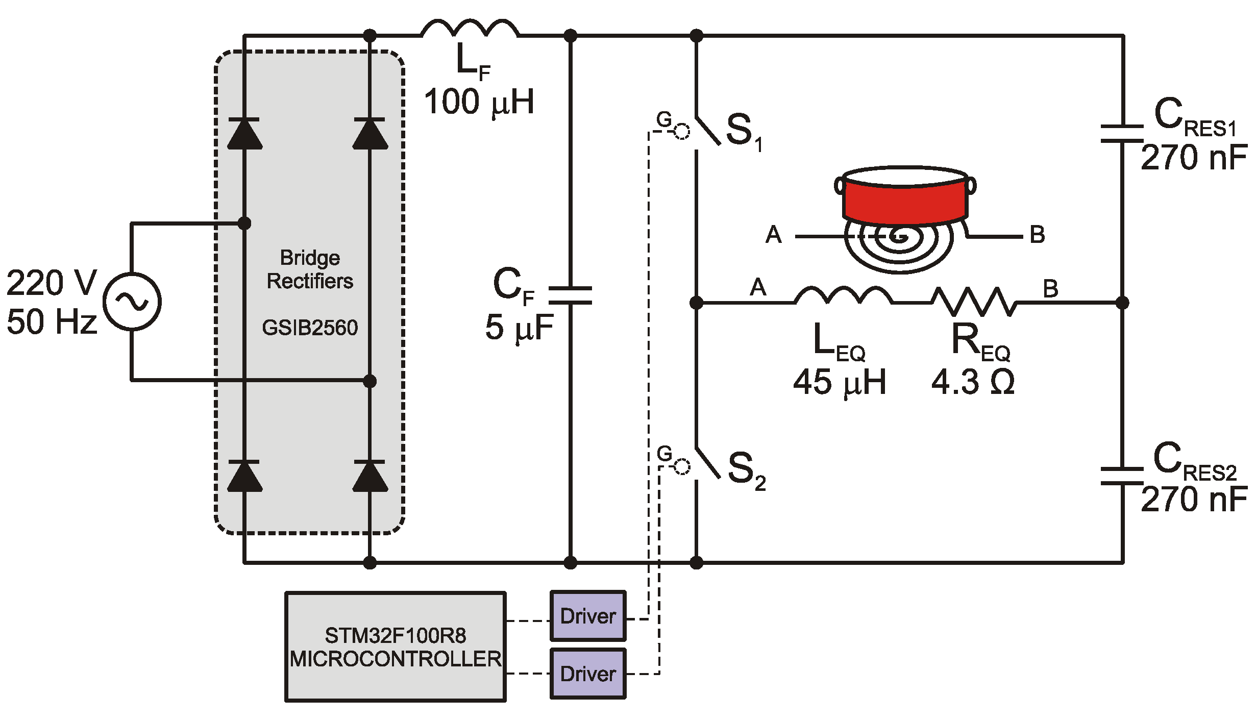
To compare the performances of power devices in DIHS, the SR HB circuit shown in Figure 5 has been realized. The main supply voltage is selected 220 V. The resonant capacitance value is 540 nF, and the equal resonant inductance and resistance values are 45 µH and 4.3 Ω, respectively. Moreover, the filter capacitance and inductance values are 5 µF and 100 µH, respectively, which are suitable for home appliance usage. The circuit was operated in a 200 W to 1800 W power range and a 45 kHz to 125 kHz switching frequency range. After 50 kHz switching frequency, a negligibly low (220 pF) capacitor is added to the switch terminals as a snubber capacitor.
Firstly SiC cascode JFET, which has not been used before, was chosen to compare semiconductor devices in DIHS systems. Then, Si and SiC power devices with nearly the same current and voltage values were selected for comparison. In addition, SiC devices from the same manufacturer at different voltage levels were used for comparison. The type, material, manufacturer company, product code of devices, and electrical and thermal values of selected power devices are given in Table 3.
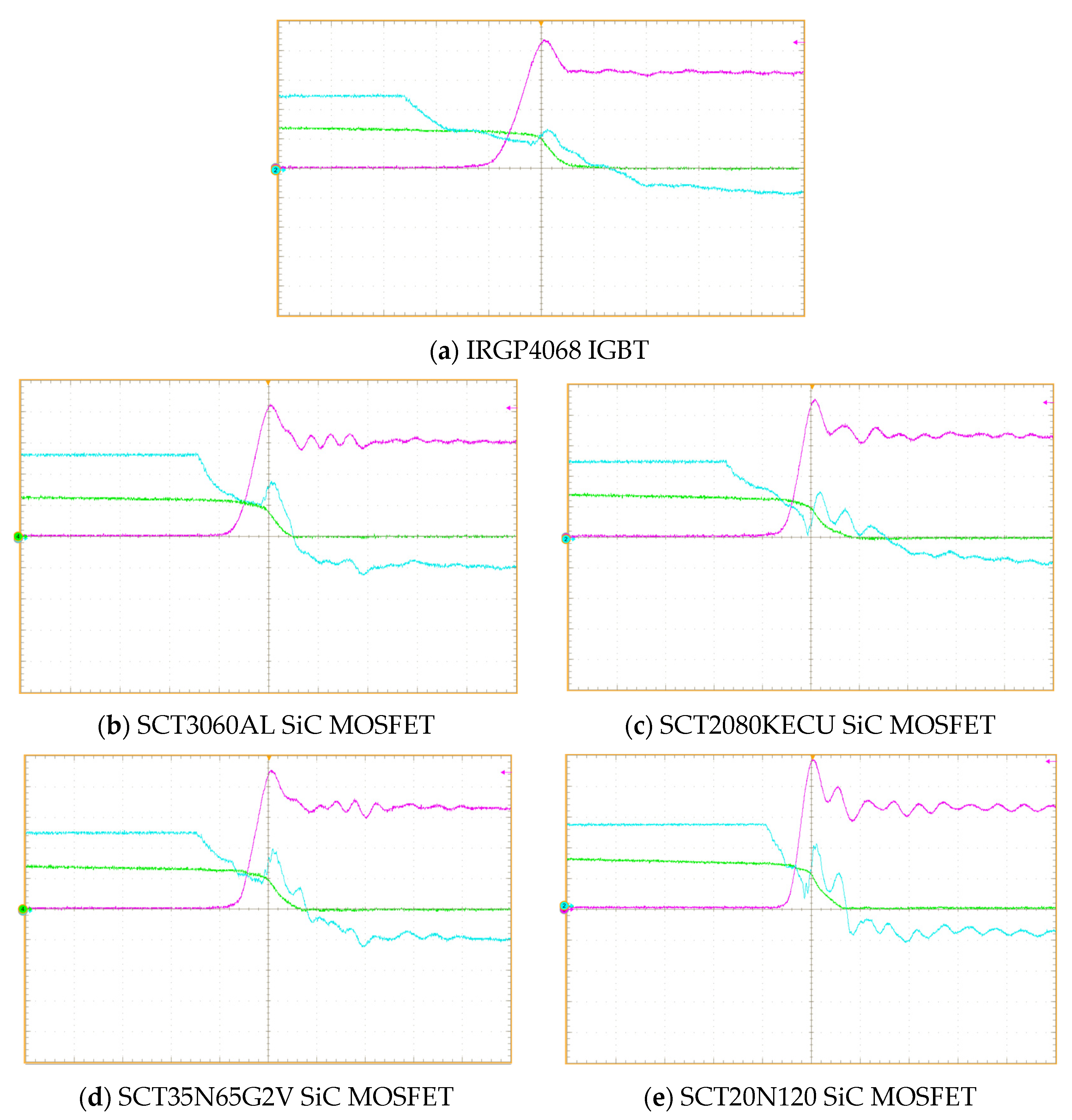
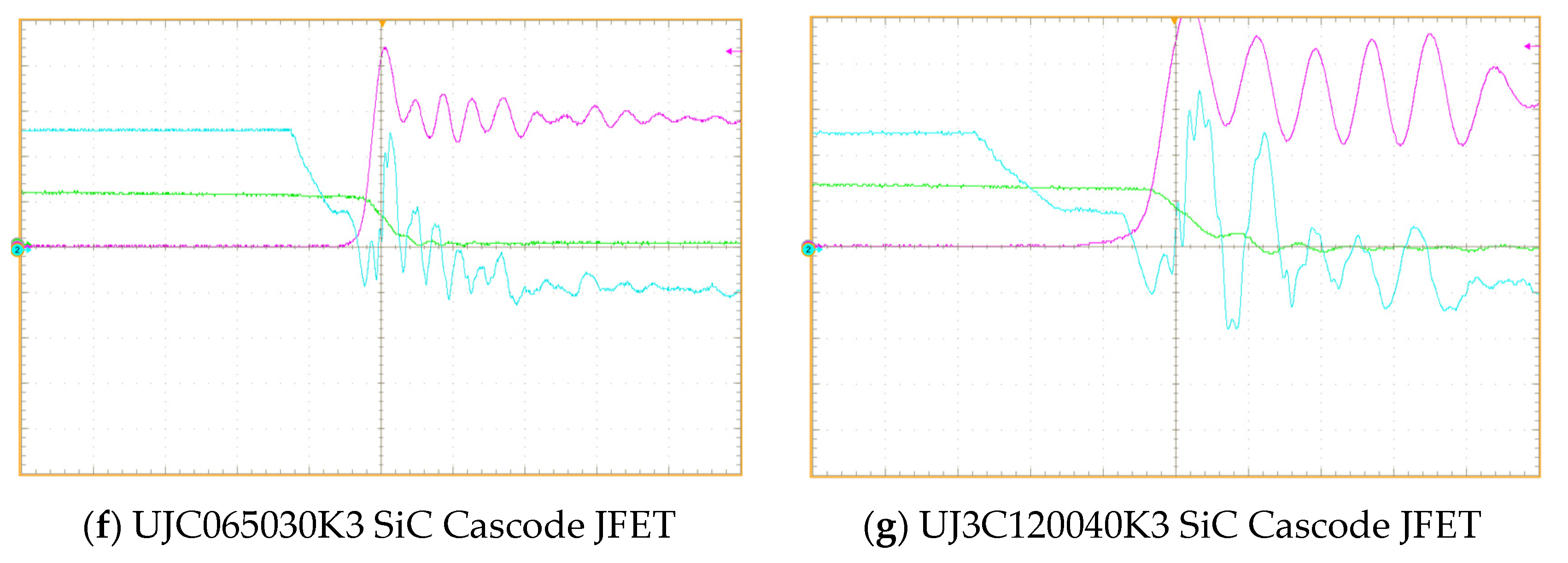
To examine the switching characteristics of the selected devices, the SR HB converter circuit is operated under a 52 kHz switching frequency and 17 A output current. The investigation of switching performance is concentrated on the turn-off transition. Since the SR HB topology operates in the inductive region, the switches turn on without loss. For this reason, the turn-on behavior of power devices has not been examined in this study. A Tektronix DPO5034B oscilloscope was used to take the measurements.
The experimental waveforms during the turn-off transition for the selected devices are given in Figure 6a–g. In these waveforms, the power device’s current, voltage, and control signals are shown in green, red, and blue colors, respectively. The switch current waveforms were obtained using the Rogowski CWT Mini 15 PEM current probe. The voltage waveforms at the switch terminals were obtained by using the PMK PHV-1000RO 1000 V 400 MHz voltage probe. Control signals were measured using a Tektronix TPP0500B 500 MHz 300 V.
From these results, at the 650 V voltage rating, it can be seen that the fastest device is the Si cascode JFET with a switching time of 168 ns, whereas the tail current of the Si IGBT almost doubles this value with 310 ns. It has been observed that the speeds of MOSFETs belonging to different companies are almost the same and are approximately 190 ns. Among the 1200 V devices, it is seen that SCT20N120 SiC MOSFET is the fastest with 140 ns, while the other SiC MOSFET SCT2080KE is the slowest with 238 ns.
Due to the significant di/dt of the SiC Cascode JFET, excessive voltage oscillations occurred during turn-off, as seen in Figure 6f,g. The power device’s parasitic capacitance and the circuit’s leakage inductances cause these oscillations. The devices’ connections should be designed so that leakage inductance is minimal [41]. It is seen that the device with the shortest current drop time of 68 ns and the highest di/dt ratio is the SiC cascode JFET of the UJ3C120040K3S. The turn-off time of the 1200 V SCT20N120 SiC MOSFET is shorter than of the 650 V SCT3060AL. SiC power devices perform worse than Si IGBT in terms of electromagnetic interference noise because of their high di/dt value.
It has been observed that the switching losses are significantly reduced with the SiC technology, which has a low switching time. Another significant loss that affects efficiency is conduction power loss. Measurements of the on-state voltage drops have been made from Figure 6, and the results are presented in Table 4. The highest and lowest conduction voltage drops occurred in the SiC MOSFET and SiC cascode JFET devices, respectively. The IGBT device with Si is in the middle range. These values are especially important at high currents. In MOSFET devices, on the other hand, the conduction voltage drop is high because of the higher conduction on-resistance. Since the on-resistance of the MOSFET increases depending on the cube of the voltage rating, the on-resistances of 1200 V SiC MOSFETs are bigger than of the 650 V devices. As a result of this, the voltage drop values are higher than for other devices. It is seen that the device with the lowest conduction voltage drop of 0.34 V is UJ3C120040K3S, and the one with the highest is the SCT20N120 with 3.33 V.
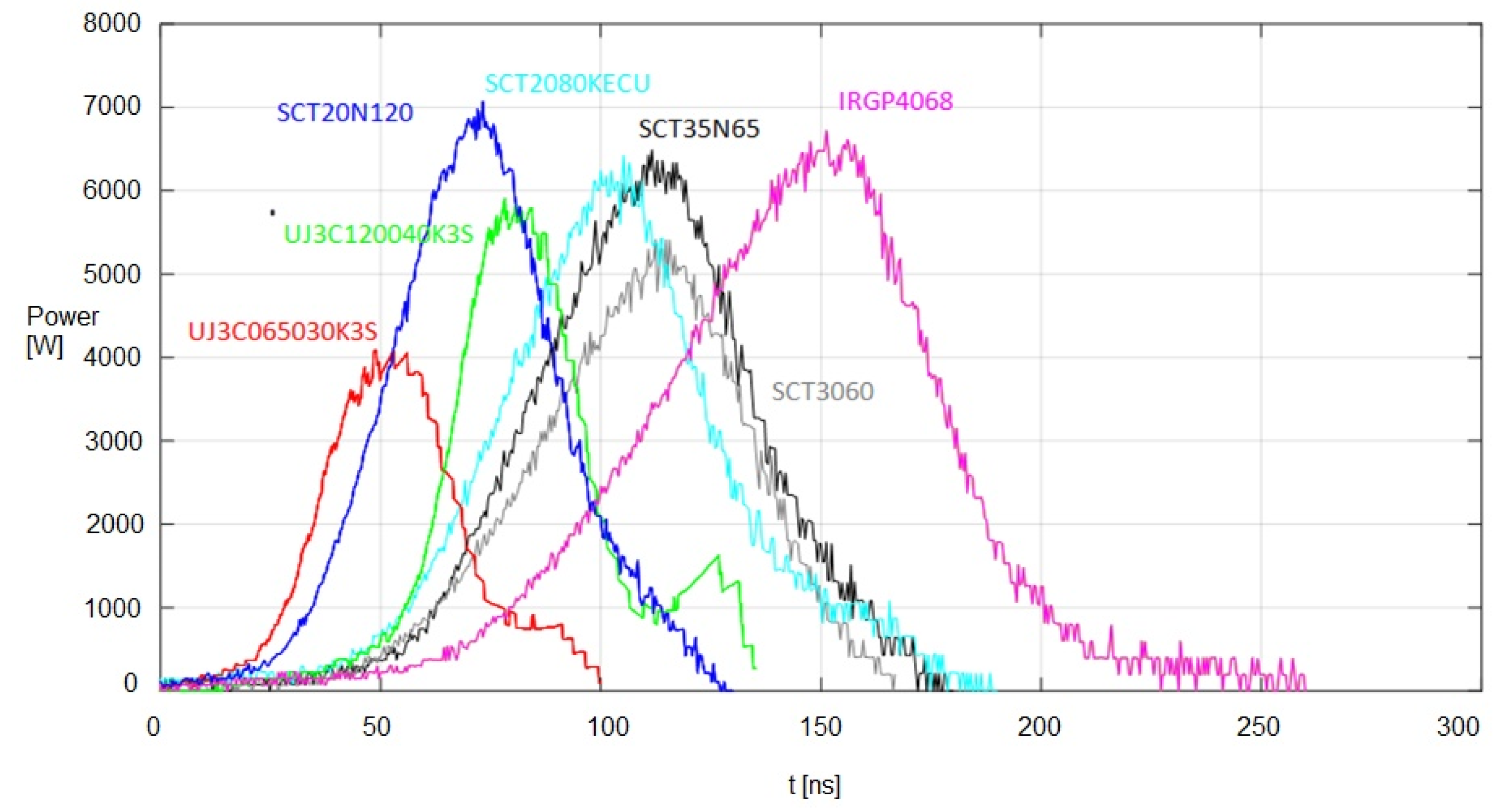
The current and voltage values during the turn-off process are taken from the oscilloscope. The variation of the power loss that occurred during the turn-off transition was obtained using these values. Figure 7 shows the change in turn-off switching power losses of devices with respect to time. From here, it is seen that the turn-off process of the IRGP4068 is 270 ns, with the current falling from 90% to 10%, and more power loss occurs under the same conditions compared to other devices. It is seen that the least power loss occurs in the UJ3C065030K3S device, and the turn-off time is approximately 100 ns.
Body diode losses are obtained by multiplying the voltage value of the diode at the moment of conduction with the current. The obtained values are given in Table 4. In terms of power loss in body diodes, it is seen that the least loss is in SCTW35N65, and the highest loss is in SCT3060AL. Although these two devices are 650 V SiC MOSFETs, they belong to different manufacturers. In addition, the power device’s turn-off energy losses are calculated by taking the derivative of the turn-off power loss waveforms according to time, as given in Equation (6). All obtained values are combined and given in Table 4.
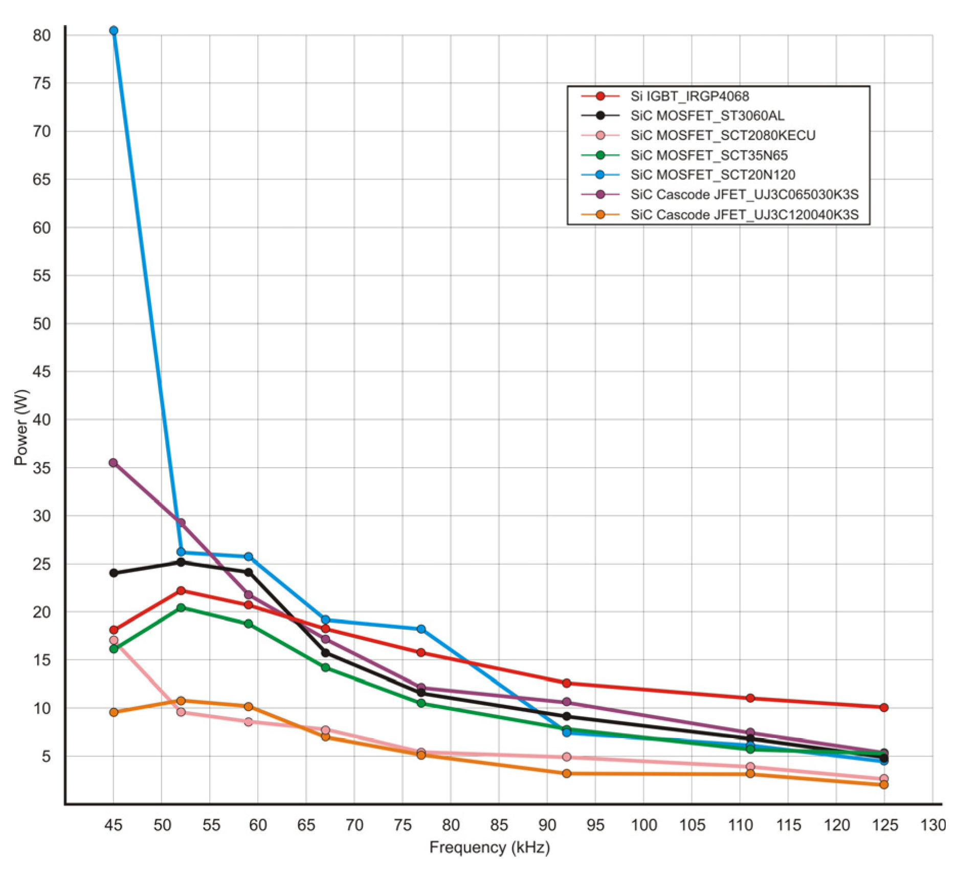
After comparing the devices’ 52 kHz switching frequency, the power devices were operated between 45 kHz and 125 kHz. The power transferred to the output with frequency has been changed. The device’s conduction and switching power losses were measured in this case. Conduction, turn-off, and total power losses of the power devices at different frequencies are given in Figure 8, Figure 9 and Figure 10, respectively. As the switching frequency moves away from the resonant frequency, that is, as the switching frequency increases, as in Table 5, the power transferred to the output decreases and the current passing through the circuit decreases. As can be seen from Figure 8, the conduction losses of the power devices decrease with increasing frequency. As seen in Figure 3, the current value before turning off affects the switching power loss. Since the current decreases with increasing switching frequency, the switching power loss decreases with current, but increases proportionally with frequency, as can be seen from Equation (3). In addition, the small value snubber capacitor connected after 50 kHz has an effect on reducing losses. As a result, in Figure 9, the variation of the switching losses does not follow an increase in direct proportion to the frequency.
In the case of operation with a 45 kHz switching frequency, that is, at 1800 W output power, the current passing through the circuit is high. From Figure 8, in this case a conduction loss of approximately 80 W occurred in the SCT20N120 device with the highest conduction voltage drop. A loss of about 8 W occurred in the UJ3C120040K3S, which has the lowest conduction voltage drop. It has been determined that the ratio of the losses of the two devices is 1/10. Similar results are valid for high frequencies. There is the same ratio between the conduction voltage drops given in Table 4.
From Figure 9, the highest switching loss occurs in the IRGP4068 in the determined operating frequency range. There is a loss of about 9.4 W at 125 kHz operating frequency. The lowest loss belongs to the SiC cascode JFET device with 1.9 W. In Figure 10, the frequency-dependent variation of the sum of the power losses in the switch is given. The SiC cascode JFET, the UJ3C120040K3S, has the lowest total losses compared to other devices in the selected frequency range. About 2 W at 200 W power and about 10 W at 1800 W power is lost. The rate of losses in the device decreases at high powers.
The efficiency of DIHS is obtained for different switching frequencies. The input and output powers of the circuit were measured using a power analyzer. Efficiency values are calculated by proportioning the measured output and input powers. To compare the efficiency of the selected devices, the tests are carried out under the same conditions.
The efficiency curves of the system depending on the switching frequency are given in Figure 11 for each switch. As seen from Figure 11, efficiency value increases significantly when the circuit is realized with SiC devices instead of Si IGBT. At all operating frequencies, the circuit efficiency with SiC cascode JFET is higher than other devices. At maximum output power, i.e., 45 kHz switching frequency, the system efficiency is 99% with the UJ3C120040K3S. The most efficient operation has been achieved with this device in all of the selected frequency ranges. In the case of using the IRGB4068 as a switch, the efficiency was measured as 97.2% at low frequencies and 89.4% at high frequencies.

6. Discussion

In this study, performance criteria for selected SiC-based devices were defined and evaluated. WBG devices will play an important role in the realization of high-performance IH systems in the near future. Engineers working in the field of design and application should know the features of these devices well. The devices were compared according to the performance criteria determined using the DIHS application circuit in Figure 12.
Experimental results show that SiC cascode JFET gives the best performance among the power devices selected for use in the DIHS. In addition, the SiC cascode JFET is advantageous in terms of applicability compared to other SiC devices, as it can be driven with the drive circuit of the Si IGBT. SiC cascode JFET has a flat efficiency curve, as well as highly efficient operation throughout the selected switching-frequency range. This feature allows efficient energy transfer to ferromagnetic and nonferromagnetic metals using the same DIHSs. Efficient operation can be achieved without overheating and without damaging the system in nonferromagnetic loads with low resistance value at high frequencies by using WBG devices in the HB converter.
The switching power losses of the SiC power devices are lower than the Si IGBT. Especially the high voltage rating SiC MOSFET has high conduction losses because of its high on-state resistance. The switching speed of Si IGBT is lower than the SiC device because of the tail current.
As a result, the turn-off power loss is higher than SiC devices. It has been determined that the parameters examined in devices with the same values belonging to different companies, except for PBD, are approximately similar. Considering the voltage and cost the device will be exposed to in the circuit, selecting the appropriate device is important in terms of efficiency and cost balance. The increasing use of SiC cascode JFET is due to industrial interest and reduced oscillations in switching.

7. Conclusions

This article presented an experimental comparative evaluation of different SiC power devices in DIHS with a state-of-the-art Si device. Detailed analyses were made using different SiC devices with the same and different voltage values from different manufacturers. The efficiency of DIHS has been investigated by operating the devices under different frequencies at the range of 45 kHz–145 kHz. As a conclusion of this study, several differential features have been identified:
  • As with the state-of-the-art Si IGBTs, the SiC Cascode JFET device, which combines the good features of two different devices, showed the best performance;
  • SiC cascode JFET is advantageous in terms of applicability compared to other SiC devices, as it can be driven with the drive circuit of the Si IGBT;
  • SiC cascode JFET has a flat efficiency curve, as well as a not only highly efficient operation throughout the selected switching frequency range.
In device selection, cost/performance balance is as effective as electrical parameters and efficiency values. Despite the cost disadvantage, using SiC power devices is increasing in industrial applications.
One of the main goals in state-of-the-art DIHS is to efficiently transfer power to all metals, ferromagnetic or nonferromagnetic. In future studies, power transfer to all metals in a converter operating efficiently at high frequency with WBG devices will be experimentally investigated. In addition, the use of WBG devices in DIHS is of great importance for sustainability and reducing carbon footprints.

Author Contributions

Conceptualization, S.A., M.O. and N.A.; methodology, S.A., M.O. and N.A.; validation, S.A., M.O. and N.A.; investigation, S.A., M.O. and N.A.; writing—original draft preparation, S.A., M.O. and N.A.; writing—review and editing, S.A., M.O. and N.A. All authors have read and agreed to the published version of the manuscript.

Funding

This research received no external funding.

Data Availability Statement

No new data were created.

Acknowledgments

This work was supported by the Scientific and Technological Research Council of Turkey and co-financed by the Mamur Technology Systems Research and Development Center under Project 3210188.

Conflicts of Interest

The authors declare no conflict of interest.

Nomenclature

CRES1, CRES2Resonance capacitorsPnNominal powerTJMMaximum operating junction temperature
CS1, CS2Snubber capacitorsPOFFTurn-off power losstOFFTurn-off time
D1, D2Freewheeling diodesPONTurn-on power losstrRise time
di/dtCurrent rate of changePSWSwitching power lossVACminAC minimum voltage
fRESResonance frequencyPTTotal power lossesVGGate voltage
fSWSwitching frequencyRDSonOn resistanceVnNominal voltage
InNominal currentREQEquivalent resistanceVONSaturation voltage
LEQEquivalent inductanceRJCThermal resistance junction-to-caseEOFFTurn-off switching loss
PBDBody diode power lossT1, T2Power devicesEONTurn-on switching loss
PCONConduction power losstdDelay timeESWSwitching loss
PMMaximum power losstfFall timeηEfficiency

References

  1. CREE. Application Considerations for Silicon Carbide MOSFETs under Power Appl. Notes. 2011. Available online: https://www.mouser.com/pdfDocs/Cree-Application-Considerations-for-Silicon-Carbide-MOSFETs.pdf (accessed on 11 December 2022).
  2. Sarnago, H.; Lucia, O.; Burdio, J.M. Interleaved resonant boost inverter featuring SiC module for high-performance induction heating. IEEE Trans. Power Electron. 2017, 32, 1018–1029. [Google Scholar] [CrossRef]
  3. Prado, E.O.; Bolsi, P.C.; Sartori, H.C.; Pinheiro, J.R. An Overview about Si, Superjunction, SiC and GaN Power MOSFET Technologies in Power Electronics Applications. Energies 2022, 15, 5244. [Google Scholar] [CrossRef]
  4. Górecki, P.; Górecki, K.; Kisiel, R.; Brzozowski, E.; Bar, J.; Guziewicz, M. Investigations of an Influence of the Assembling Method of the Die to the Case on Thermal Parameters of IGBTs. IEEE Trans. Compon. Packag. Manuf. Technol. 2021, 11, 1988–1996. [Google Scholar] [CrossRef]
  5. Li, K.; Evans, P.; Johnson, M. SiC/GaN power semiconductor devices: A theoretical comparison and experimental evaluation under different switching conditions. IET Electr. Syst. Transp. 2018, 8, 3–11. [Google Scholar] [CrossRef]
  6. Nakamura, T.; Nakano, Y.; Aketa, M.; Hanada, T. Recent Development and Future Prospects of Power SiC Devices. In Proceedings of the 2014 International Power Electronics Conference (IPEC-Hiroshima 2014-ECCE ASIA), Hiroshima, Japan, 18–21 May 2014; Volume 720, p. 2074. [Google Scholar] [CrossRef]
  7. Nagy, I. Inverters-Resonant Converters; CRC: Boca Raton, FL, USA, 2002. [Google Scholar]
  8. Kotzea, S.; Debald, A.; Heuken, M.; Kalisch, H.; Vescan, A. Demonstration of a GaN-Based Vertical-Channel JFET Fabricated by Selective-Area Regrowth. IEEE Trans. Electron Devices 2018, 65, 5329–5336. [Google Scholar] [CrossRef]
  9. Pittini, R.; Zhang, Z.; Andersen, M.A.E. SiC JFET Cascode Loss Dependency on the MOSFET Output Capacitance and Performance Comparison with Trench IGBTs. In Proceedings of the 2013 Twenty-Eighth Annual IEEE Applied Power Electronics Conference and Exposition (APEC), Long Beach, CA, USA, 17–21 March 2013; pp. 1287–1293. [Google Scholar] [CrossRef]
  10. Josifović, I.; Popović-Gerber, J.; Ferreira, J.A. Improving SiC JFET switching behavior under influence of circuit parasitics. IEEE Trans. Power Electron. 2021, 27, 3843–3854. [Google Scholar] [CrossRef]
  11. Haehre, K.; Meisser, M.; Denk, F.; Kling, R.; Heering, W. Switching Speed-Control of an Optimized Capacitor-Clamped Normally-on Silicon Carbide JFET Cascode. In Proceedings of the 15th International Power Electronics and Motion Control Conference (EPE/PEMC), Novi Sad, Serbia, 4–6 September 2012. [Google Scholar] [CrossRef]
  12. Sarnago, H.; Lucia, O.; Mediano, A.; Burdio, J.M. Design and implementation of a high-efficiency multiple-output resonant converter for induction heating applications featuring wide bandgap devices. IEEE Trans. Power Electron. 2014, 29, 2539–2549. [Google Scholar] [CrossRef]
  13. Ning, P.; Zhang, D.; Lai, R.; Jiang, D.; Wang, F.; Boroyevich, D.; Burgos, R.; Karimi, K.; Immanuel, V.D.; Solodovnik, E.V. High-temperature hardware: Development of a 10-kW high-temperature, high-power-density three-phase ac-dc-ac SiC converter. IEEE Ind. Electron. Mag. 2013, 7, 6–17. [Google Scholar] [CrossRef]
  14. Esteve, V.; Jordan, J.; Sanchis-Kilders, E.; Dede, E.J.; Maset, E.; Ejea, J.B.; Ferreres, A. Comparative study of a single inverter bridge for dual-frequency induction heating using Si and SiC MOSFETs. IEEE Trans. Ind. Electron. 2015, 62, 1440–1450. [Google Scholar] [CrossRef]
  15. Jordan, J.; Esteve, V.; Sanchis-Kilders, E.; Dede, E.J.; Maset, E.; Ejea, J.B.; Ferreres, A. A comparative performance study of a 1200 v Si and SiC MOSFET intrinsic diode on an induction heating inverter. IEEE Trans. Power Electron. 2014, 29, 2550–2562. [Google Scholar] [CrossRef]
  16. Millan, J.; Godignon, P.; Perpina, X.; Perez-Tomas, A.; Rebollo, J. A survey of wide bandgap power semiconductor devices. IEEE Trans. Power Electron. 2014, 29, 2155–2163. [Google Scholar] [CrossRef]
  17. Moreland, W.C. Induction Its Performance Development Problems. IEEE Trans. Ind. Appl. 1973, 1A-9, 81–85. [Google Scholar] [CrossRef]
  18. Kazimierczuk, M.K.; Dariusz, C. Resonant Power Converters, 2nd ed.; John Wiley & Sons, Inc., Publication: Hoboken, NJ, USA, 2011. [Google Scholar]
  19. Dzieniakowski, M.A. Power Electronics Converters in Induction Heating—The Survey. In Proceedings of the 2017 Progress in Applied Electrical Engineering (PAEE), Koscielisko, Poland, 25–30 June 2017. [Google Scholar] [CrossRef]
  20. Ozturk, M.; Zungor, F.; Emre, B.; Oz, B. Quasi Resonant Inverter Load Recognition Method. IEEE Access 2022, 10, 89376–89386. [Google Scholar] [CrossRef]
  21. Vishnuram, P.; Ramachandiran, G.; Babu, T.S.; Nastasi, B. Induction heating in domestic cooking and industrial melting applications: A systematic review on modelling, converter topologies and control schemes. Energies 2021, 14, 6634. [Google Scholar] [CrossRef]
  22. Sarnago, H.; Lucía, Ó.; Burdío, J.M. A Comparative Evaluation of SiC Power Devices for High-Performance Domestic Induction Heating. IEEE Trans. Ind. Electron. 2015, 62, 4795–4804. [Google Scholar] [CrossRef]
  23. Shijo, T.; Kurachi, S.; Noda, Y.; Yamada, H.; Tanaka, T. A 400 kHz SiC-MOSFETs High-Frequency Inverter for Small-Foreign-Metal Particle Detection. In Proceedings of the 2016 IEEE 2nd Annual Southern Power Electronics Conference (SPEC), Auckland, New Zealand, 5–8 December 2016; pp. 3–7. [Google Scholar] [CrossRef]
  24. Ogiwara, H.; Itoi, M.; Nakaoka, M. Highly Efficient High Frequency Inverter for Induction Heating Using SiC Power Module. In Proceedings of the 2016 IEEE International Power Electronics and Motion Control Conference (PEMC), Varna, Bulgaria, 25–28 September 2016; Volume 5, pp. 116–121. [Google Scholar] [CrossRef]
  25. Komeda, S.; Tsuboi, Y.; Fujita, H. Inverter for Industrial Induction Heating Systems. In Proceedings of the 2014 International Power Electronics Conference (IPEC-Hiroshima 2014-ECCE ASIA), Hiroshima, Japan, 18–21 May 2014; pp. 1160–1165. [Google Scholar]
  26. Aunsborg, T.S.; Duun, S.B.; Munk-Nielsen, S.; Uhrenfeldt, C. Development of a current source resonant inverter for high current MHz induction heating. IET Power Electron. 2022, 15, 1–10. [Google Scholar] [CrossRef]
  27. Gaudó, P.M.; Bernal, C.; Otín, A.; Burdío, J.M. Silicon carbide JFET resonant inverter for induction heating home appliances. In Proceedings of the IECON 2011-37th Annual Conference of the IEEE Industrial Electronics Society, Melbourne, VIC, Australia, 7–10 November 2011; pp. 2551–2556. [Google Scholar] [CrossRef]
  28. Sarnago, H.; Lucia, O.; Mediano, A.; Burdio, J.M. A class-e direct AC-AC converter with multicycle modulation for induction heating systems. IEEE Trans. Ind. Electron. 2014, 61, 2521–2530. [Google Scholar] [CrossRef]
  29. Valchev, V.C.; Mareva, D.J. Considerations for components selection of inverter for induction heating. In Proceedings of the 2016 25th International Scientific Conference Electronics (ET), Sozopol, Bulgaria, 12–14 September 2016; pp. 38–41. [Google Scholar] [CrossRef]
  30. Mishima, T.; Morinaga, S.; Nakaoka, M. All-SiC power module-applied single-stage ZVS-PWM AC-AC converter for high-frequency induction heating. In Proceedings of the IECON 2015-41st Annual Conference of the IEEE Industrial Electronics Society, Yokohama, Japan, 9–12 November 2015; pp. 004211–004216. [Google Scholar] [CrossRef]
  31. Laloya, E.; Lucia, O.; Concha, J.; Burdio, J.M. Experimental evaluation of dynamic load changes in flexible induction heating appliances. In Proceedings of the IECON 2014-40th Annual Conference of the IEEE Industrial Electronics Society, Dallas, TX, USA, 29 October–1 November 2014; pp. 3227–3232. [Google Scholar] [CrossRef]
  32. Cha, K.-H.; Ju, C.-T.; Kim, R.-Y. Analysis and Evaluation of WBG Power Device in High Frequency Induction Heating Application. Energies 2020, 13, 5351. [Google Scholar] [CrossRef]
  33. Shijo, T.; Kurachi, S.; Uchino, Y.; Noda, Y.; Yamada, H.; Tanaka, T. High-frequency induction heating for small-foreign-metal particle detection using 400 kHz SiC-MOSFETs inverter. In Proceedings of the 2017 IEEE Energy Conversion Congress and Exposition (ECCE), Cincinnati, OH, USA, 1–5 October 2017; pp. 5133–5138. [Google Scholar] [CrossRef]
  34. Avellaned, J.; Bernal, C.; Otin, A.; Molina, P.; Burdio, J.M. Half-bridge resonant inverter with SiC cascode applied to domestic induction heating. In Proceedings of the 2013 Twenty-Eighth Annual IEEE Applied Power Electronics Conference and Exposition (APEC), Long Beach, CA, USA, 17–21 March 2013; pp. 122–127. [Google Scholar] [CrossRef]
  35. Bodur, H. Güç Elektroniği, 2nd ed.; Birsen Yayınevi: Istanbul, Turkey, 2012. [Google Scholar]
  36. Sarnago, H.; Lucía, Ó.; Mediano, A.; Burdío, J.M. Analytical Model of the Half-Bridge Series Resonant Inverter for Improved Power Conversion Efficiency and Performance. IEEE Trans. Power Electron. 2015, 30, 4128–4143. [Google Scholar] [CrossRef]
  37. Lucia, O.; Carretero, C.; Palacios, D.; Valeau, D.; Burdío, J.M. Configurable snubber network for efficiency optimisation of resonant converters applied to multi-load induction heating. Electron. Lett. 2011, 47, 989–991. [Google Scholar] [CrossRef]
  38. Ozturk, M.; Altintas, N. Multi-output AC–AC converter for domestic induction heating. Electr. Eng. 2022, 25, 1–20. [Google Scholar] [CrossRef]
  39. Salehifar, M.; Moreno-Eguilaz, M.; Sala, V.; Romeral, L. A novel AC-AC converter based SiC for domestic induction cooking applications. In Proceedings of the 2013 Twenty-Eighth Annual IEEE Applied Power Electronics Conference and Exposition (APEC), Long Beach, CA, USA, 17–21 March 2013; pp. 3216–3223. [Google Scholar] [CrossRef]
  40. Sarnago, H.; Lucia, O.; Mediano, A.; Burdio, J.M. Direct AC-AC resonant boost converter for efficient domestic induction heating applications. IEEE Trans. Power Electron. 2014, 29, 1128–1139. [Google Scholar] [CrossRef]
  41. Aggeler, D.; Canales, F.; Biela, J.; Kolar, J.W. Dv/Dt-Control Methods for the SiC JFET/Si MOSFET Cascode. IEEE Trans. Power Electron. 2013, 28, 4074–4082. [Google Scholar] [CrossRef]
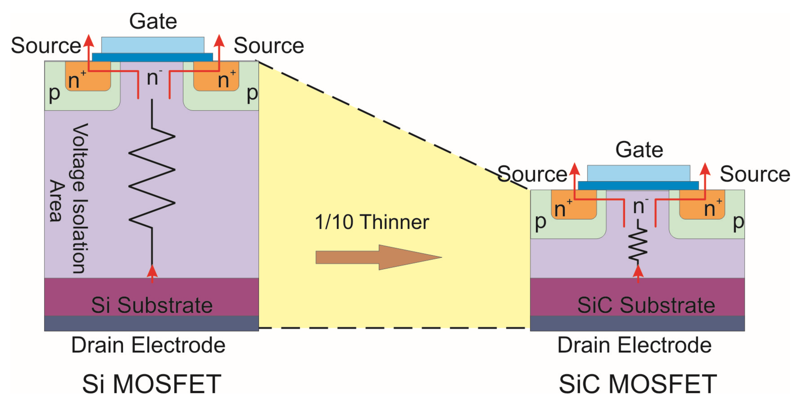
Figure 1. Comparison between Si and SiC.
Energies 16 03987 g001
Figure 2. Circuit topologies and power devices used in domestic IH systems.
Energies 16 03987 g002
Figure 3. Current, voltage, and power loss waveforms of power device.
Energies 16 03987 g003
Figure 4. SR HB circuit scheme for IH applications with Si IGBT.
Energies 16 03987 g004
Figure 5. Experimental circuit scheme.
Energies 16 03987 g005
Figure 6. Main waveforms during turn-off transition. Control signal (blue, 5 V/div), device voltage (purple, 100 V/div), and device current (green, 3 V/div); time (100 ns/div).
Energies 16 03987 g006aEnergies 16 03987 g006b
Figure 7. Turn-off switching losses of power devices.
Energies 16 03987 g007
Figure 8. Conduction losses of power devices.
Energies 16 03987 g008
Figure 9. Turn-off power losses of power devices.
Energies 16 03987 g009
Figure 10. Total losses of power devices.
Energies 16 03987 g010
Figure 11. Efficiency vs. frequency.
Energies 16 03987 g011
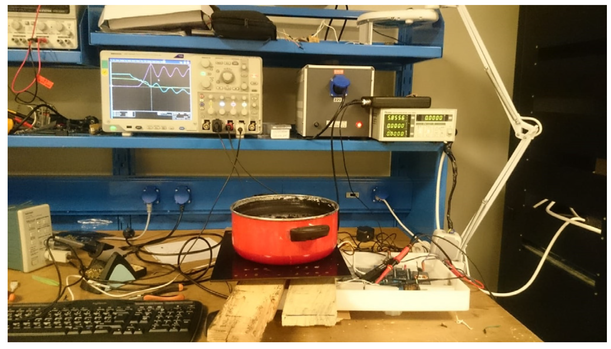
Figure 12. Photograph of the experimental setup.
Energies 16 03987 g012
Table 1. Survey of IH with WBG devices.
ReferenceTopologySiSiSiCSiCSiCSiC
IGBTMOSFETMOSFETBJTJFETCascode JFET
[23]FB X
[2]FB X
[24]HB + FB X
[25]FB X
[26]CSRI X
[27]SS QRX X
[28]QR X
[12]FB X
[14]SR HB X
[15]FB XX
[29]SR FB XX
[30]LLCXXX
[31]Boost HBX X
[32]HB X
[33]HBX XXX
PSHBX X X
PS: Present Study.
Table 2. Comparative studies.
Ref.DeviceTopologyAnalyses
Typeη VoltageCurrentPnfSWTypeFrequency
(%)(V)(A)(kW)(kHz)
[15]Si MOSFET97.31200295100FBConstanttOFF, tON,
2Si MOSFET98120024POFF, PON,
SiC MOSFET99.2120033PT, η
[30]Si IGBT95.212001002.632Boost HBConstantPOFF, PT,
SiC MOSFET97.21200120η
[27]Si IGBTN/A1200302-121.3–314SSQRVariableVON, tOFF,
SiC JFET-nONN/A120017T(°C)
[29]Si IGBT8460075650LLCVariablePT, η
Si MOSFET9160065
SiC MOSFET94120045
[22]Si IGBT96.1N/AN/220HBConstanttOFF, POFF,
SiC MOSFET95.1120042PON, PT,
SiC BJT97.8120050η,VON
SiC JFET-nON96.3120048
SiC JFET-nOFF95.7120030
PSSi IGBT97.3600480.2–1.8125–45HBVariablePT, PCON,
SiC MOSFET97.665027PSW, POFF,
SiC MOSFET98.365035PON, PBD,
SiC MOSFET96.4120028tOFF, tf,
SiC MOSFET91.5120016di/dt, VON,
SiC cascode JFET98.165062η,
SiC cascode JFET99120047
PS: Present Study.
Table 3. Some electrical and thermal characteristics of the power devices used in the experimental circuit.
CompanyProduct CodeMaterial/TypeIn (A)Vn (V)RDSon (mΩ)PM (W)VG (V)RJC (°C/W)Tm (°C)
InfineonIRGP4068DSi IGBT48600VCEon = 2 V
48 A/150 °C
170(0)–(+15)0.45(−55)–(+175)
RohmSCT3060ALSiC MOSFET2765079.2 mΩ
13 A/125 °C
80(−4)–(+22)0.91(−55)–(+175)
RohmSCT2080KESiC MOSFET281200100 mΩ
20 A/25 °C
130(−6)–(+22)0.57(−55)–(+175)
STSCT35N65SiC MOSFET3565055 mΩ
20 A/125 °C
90(−6)–(+22)0.72(−55)–(+175)
STSCT20N120SiC MOSFET161200189 mΩ
10 A/150 °C
175(−10)–(+25)1(−55)–(+200)
USCiUJ3C065030K3SSiC Cascode JFET6265040 mΩ
20 A/175 °C
210(−25)–(+22)0.34(−55)–(+175)
USCiUJ3C120040K3SSiC Cascode JFET47120060 mΩ
20 A/175 °C
210(−25)–(+22)0.35(−55)–(+175)
Table 4. Values are taken from waveforms of power devices.
toff (ns)tf (ns)di/dt (A/µs)VON (V)PBD (W)EOFF (µJ)
Si IGBTIRGP4068D3101311301.261.16497.7
SiC MOSFETSCT3060AL182921841.372.31374
SiC MOSFETSCT2080KE2381101543.092.21368
SiC MOSFETSCT35N65G195901891.571380.15
SiC MOSFETSCT20N120140712413.331.83371
SiC Cascode JFETUJ3C065030K3S168742300.931.17313
SiC Cascode JFETUJ3C120040K3S193672530.341.75460
Table 5. Frequency-dependent power values.
fSW (kHz)Output Power (W)
451800
521500
591300
66700
77500
91400
111300
125200
Disclaimer/Publisher’s Note: The statements, opinions and data contained in all publications are solely those of the individual author(s) and contributor(s) and not of MDPI and/or the editor(s). MDPI and/or the editor(s) disclaim responsibility for any injury to people or property resulting from any ideas, methods, instructions or products referred to in the content.