
Switched Inductor DC–DC Boost Regulator Using Voltage-to-Time Controller for TEG Applications


Abstract
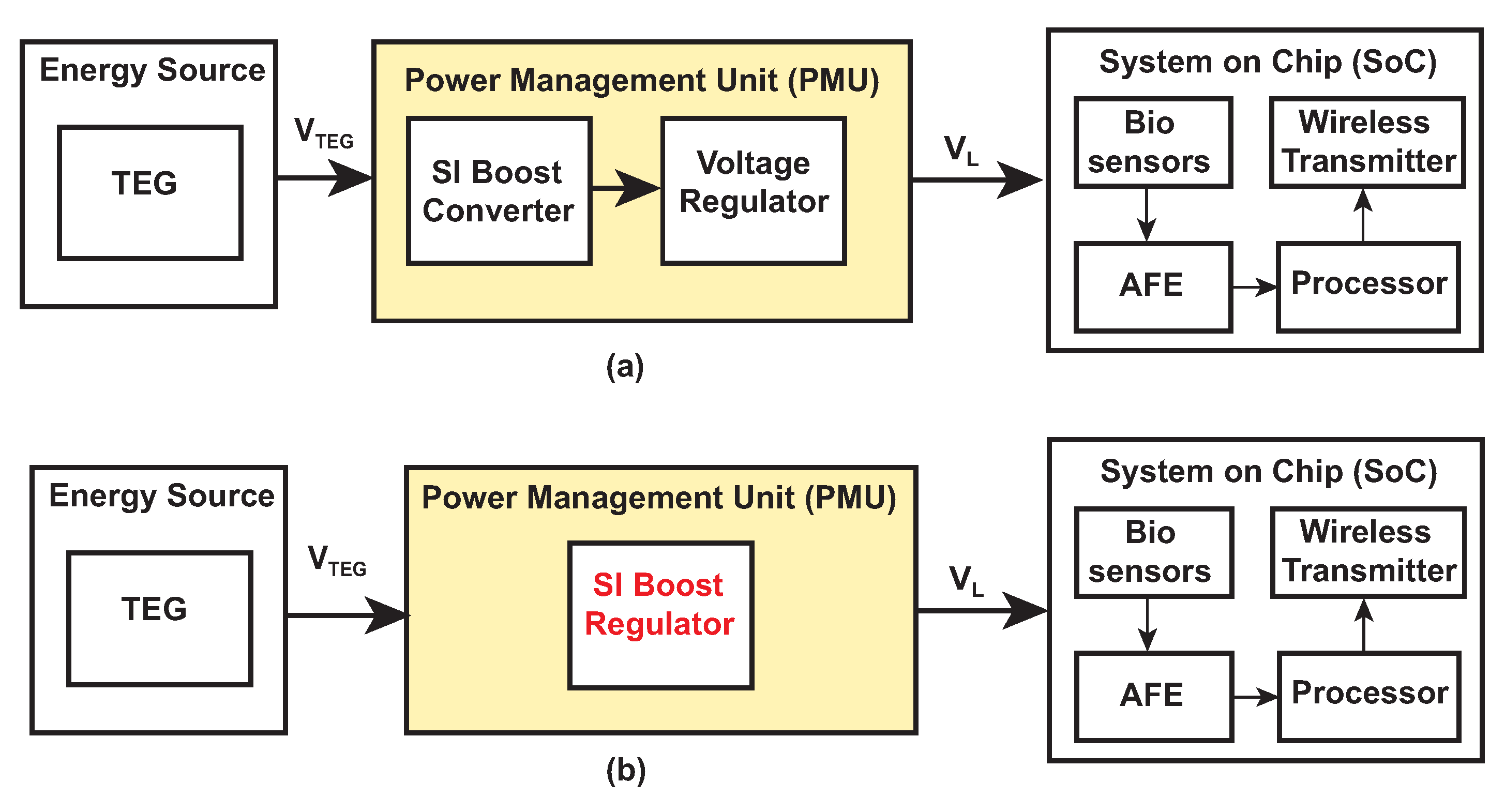
:1. Introduction
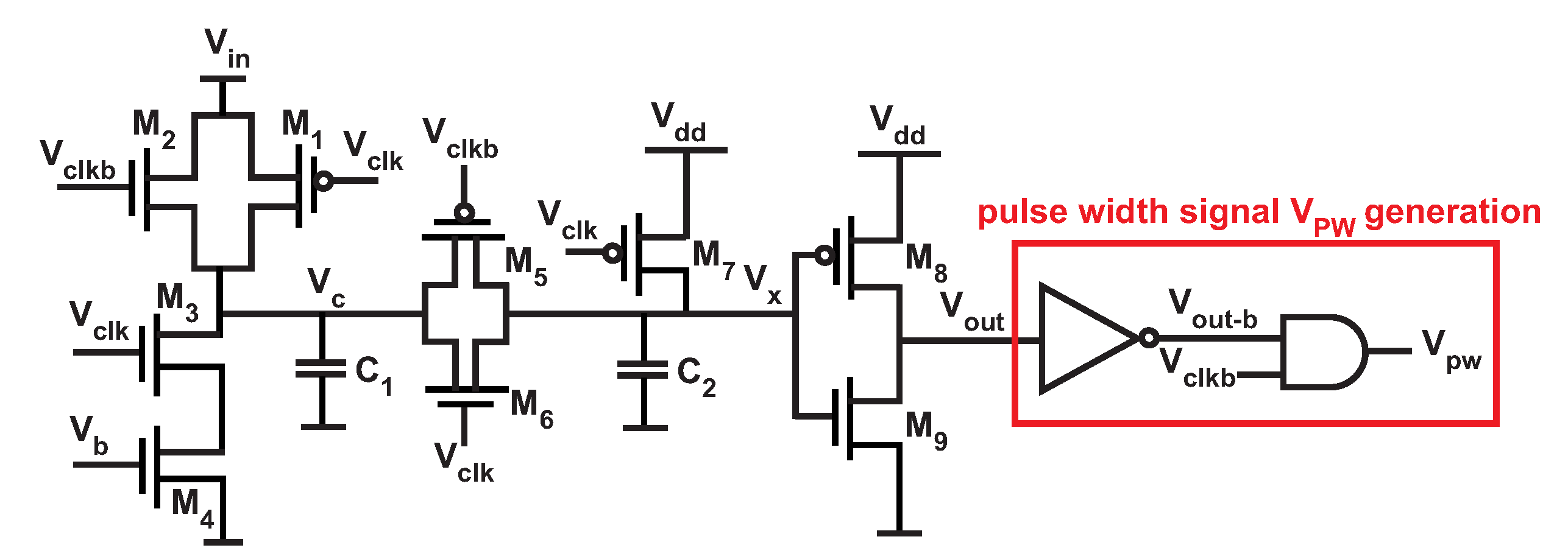
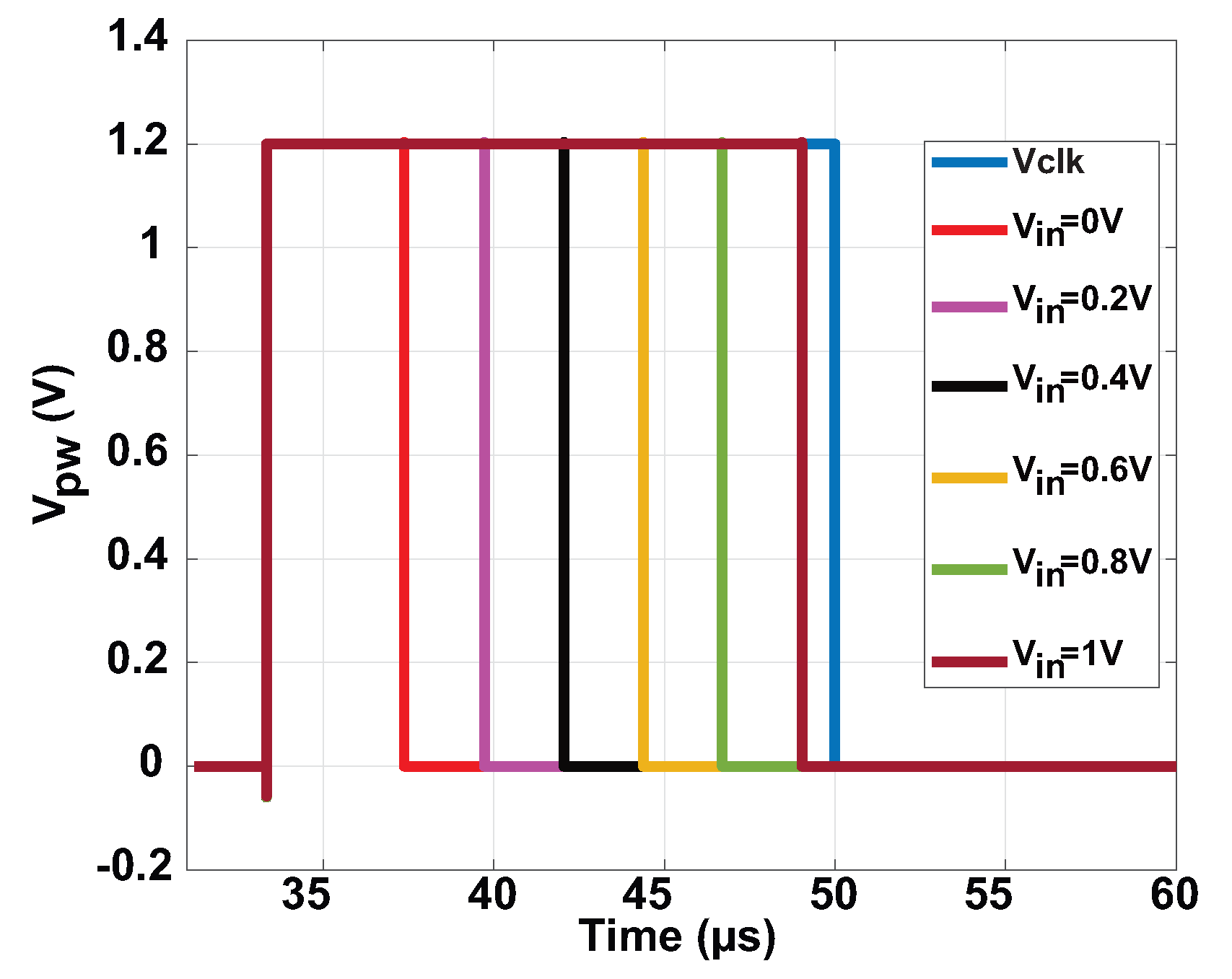
- A 6.5 W VTC circuit design that linearly converts a wide range of input voltage range between 0 to 1 V to a time delay. This design eliminates the non-linearity issue that exists in the conventional current-starved inverter delay unit. Two capacitors have been added in order to generate a linear time delay at much wider input voltage. The two capacitors act as a reservoir for charge and the delay is direct function of this charge. The capacitors’ values are selected in such a way to minimize the nonlinear effect on the delay.
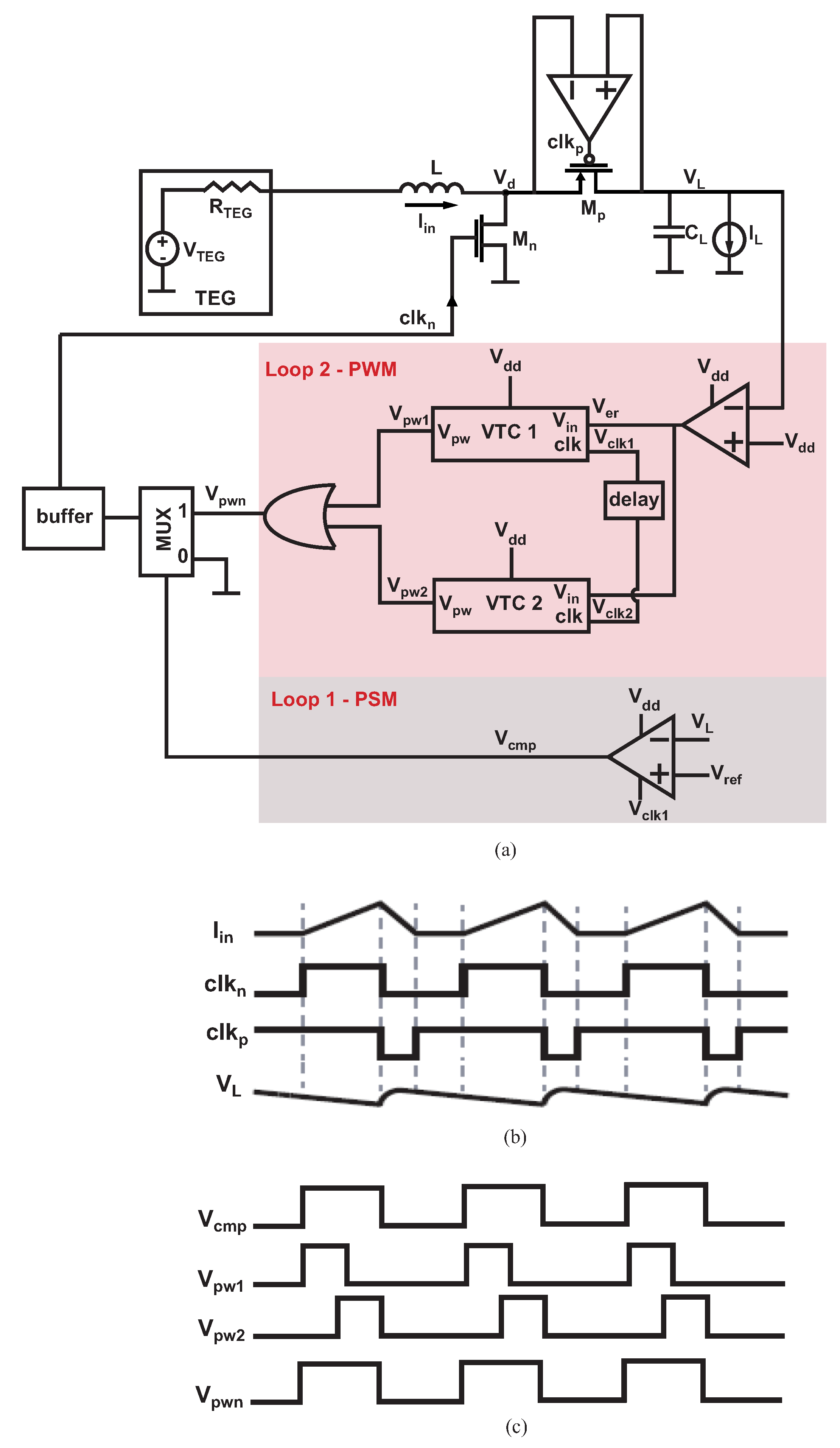
- The VTC is utilized as pulse width modulation control technique in the SI regulator to boost and regulate the voltage simultaneously.
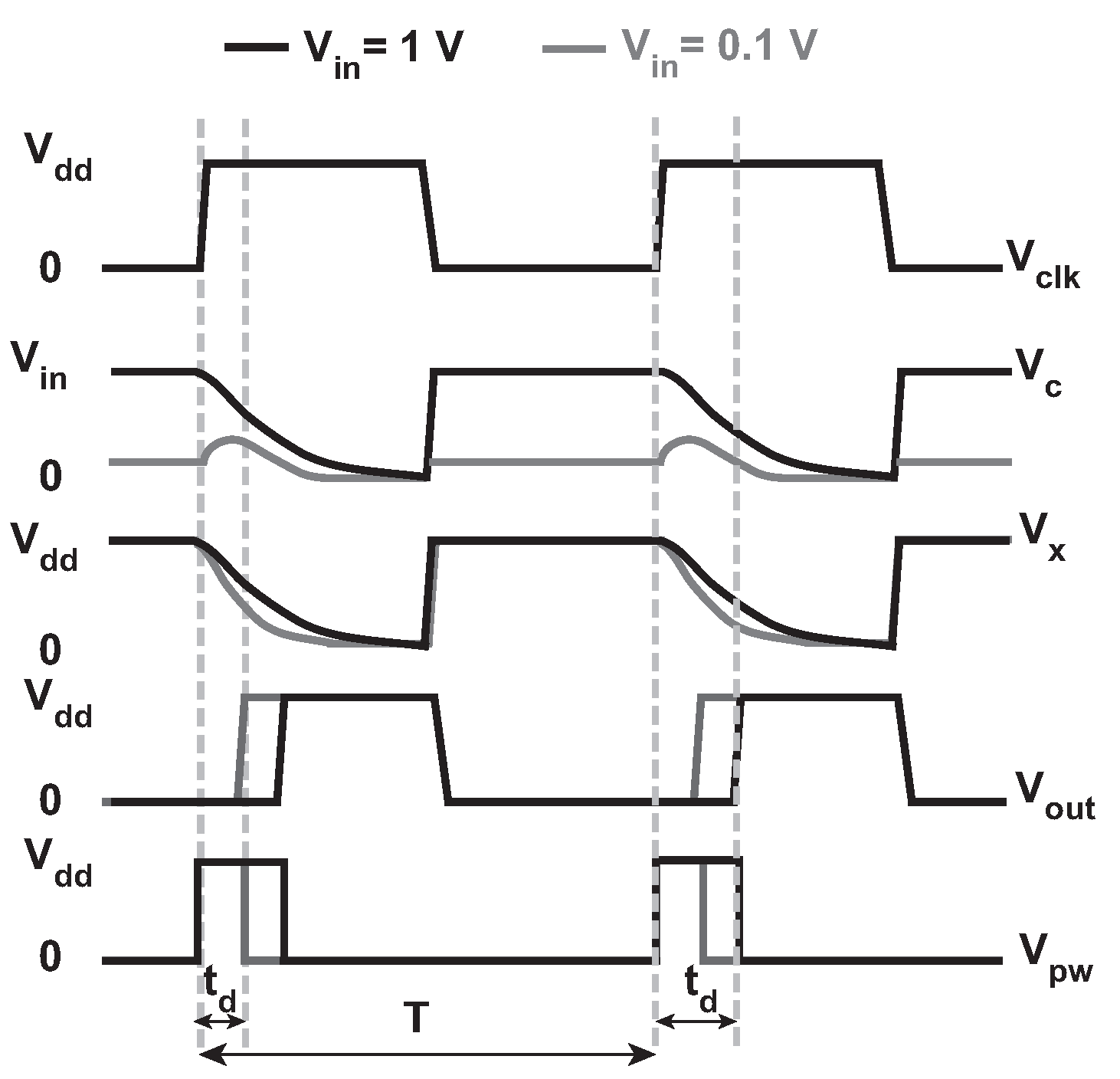
2. Voltage-to-Time Converter (VTC) Circuit Design
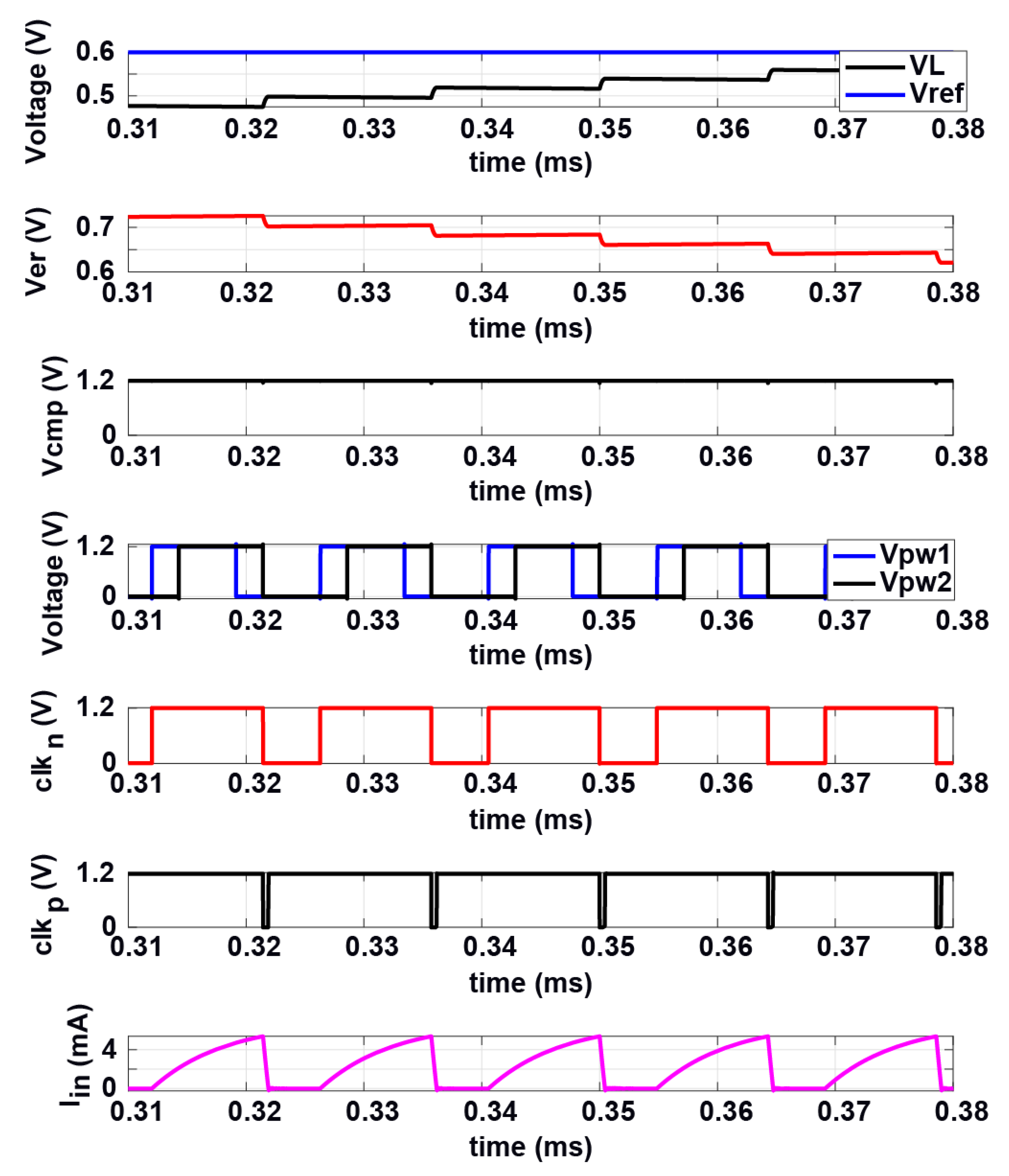
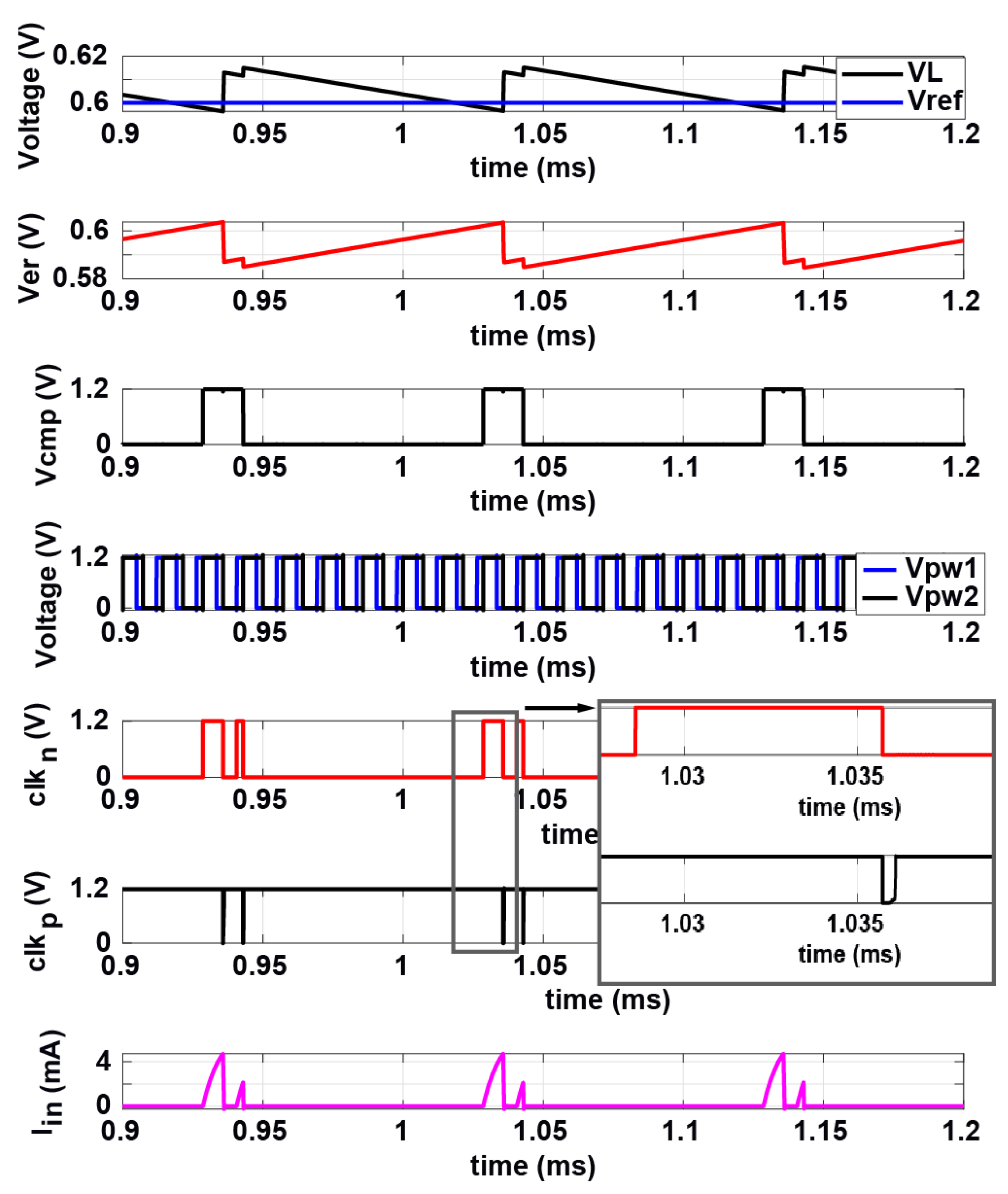
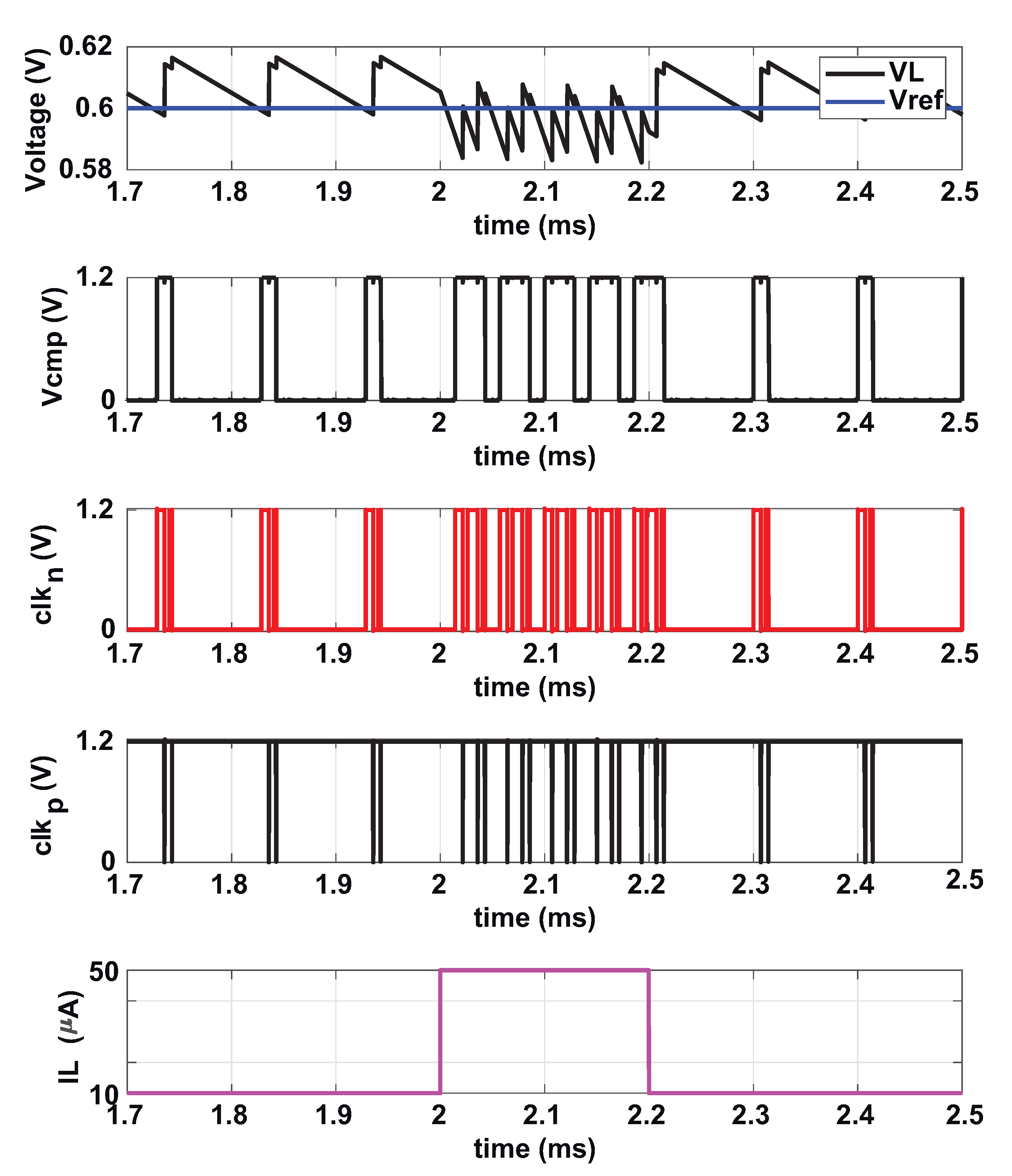
3. Switched Inductor DC–DC Boost Converter Using the Proposed VTC Circuit
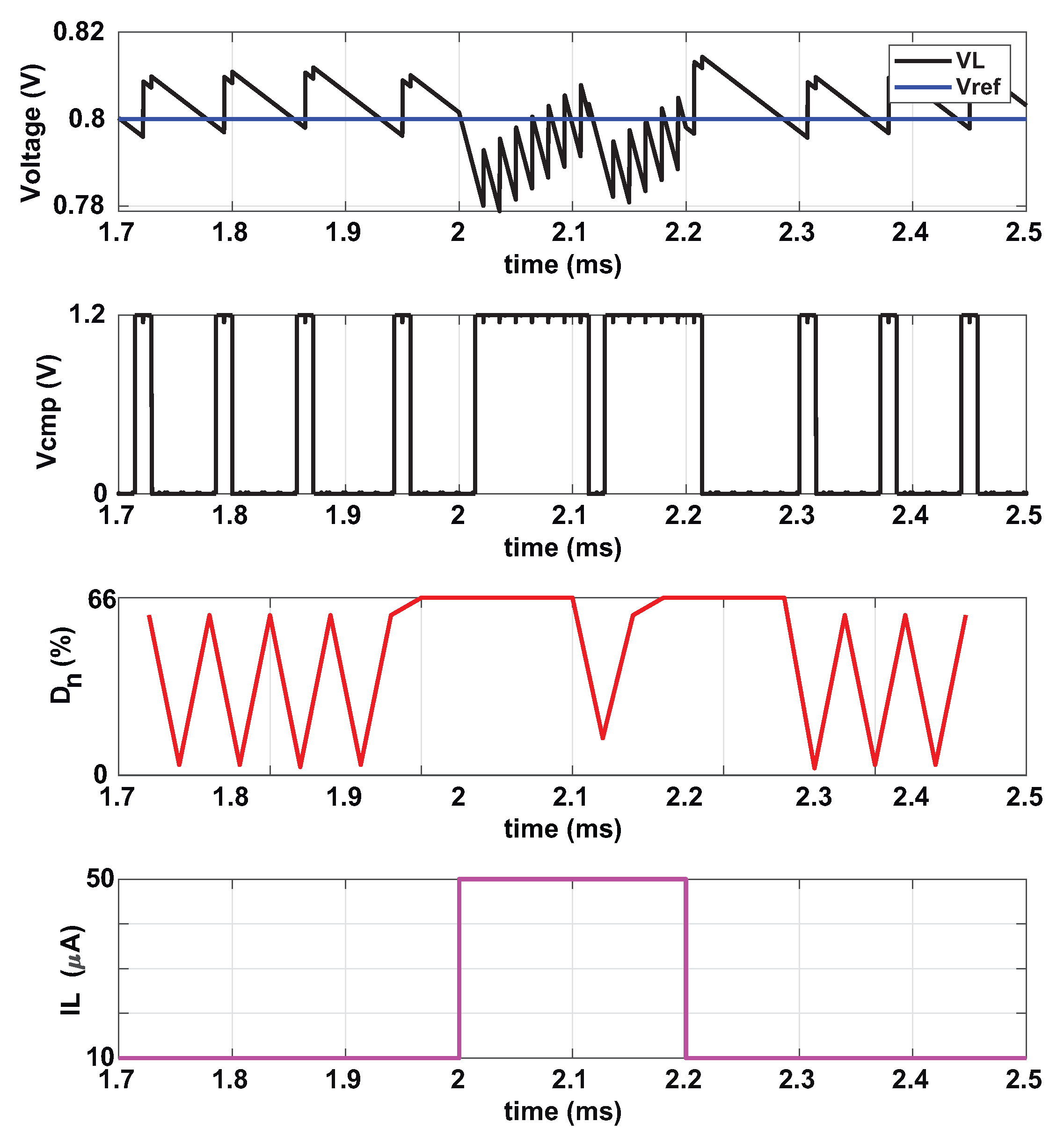
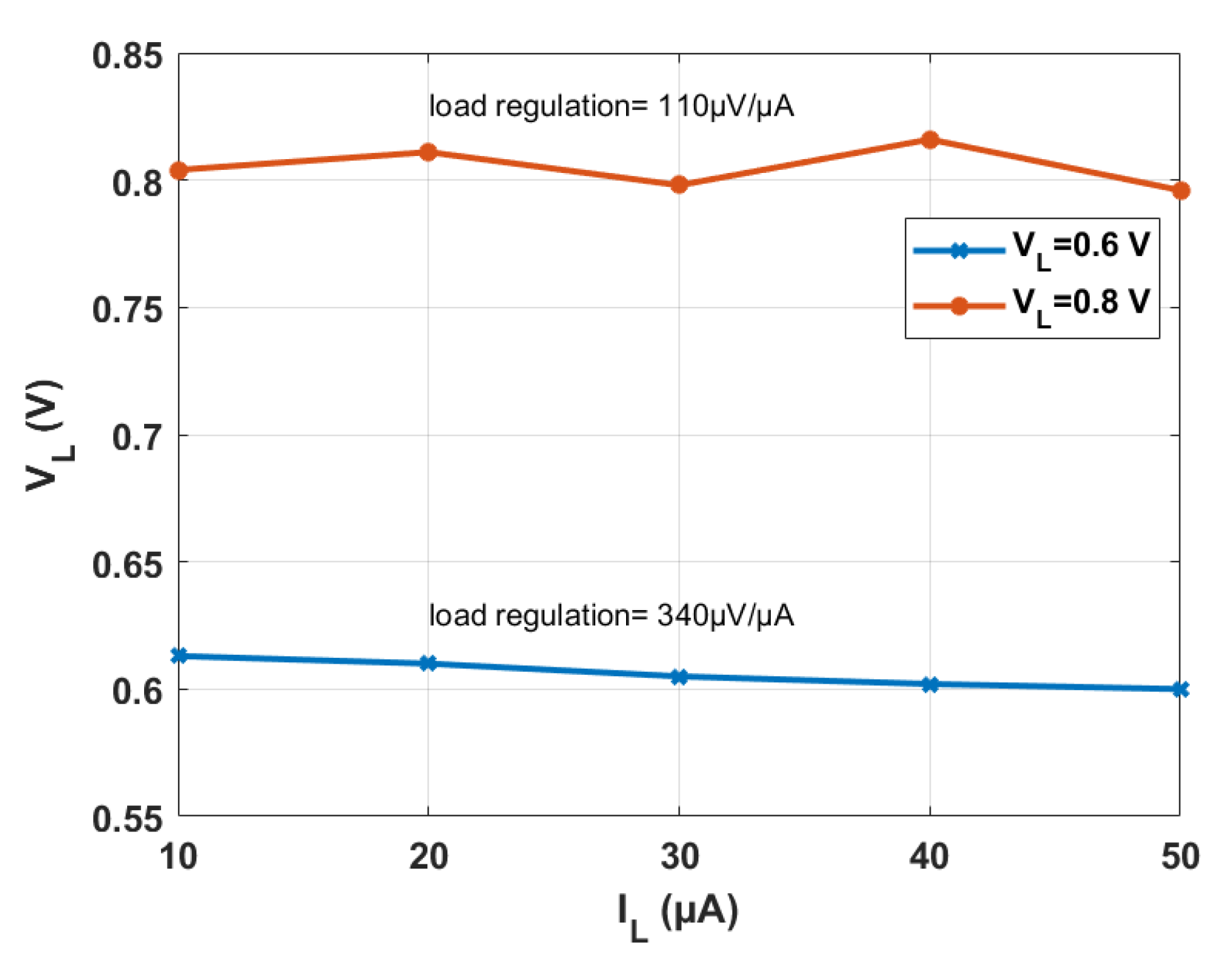
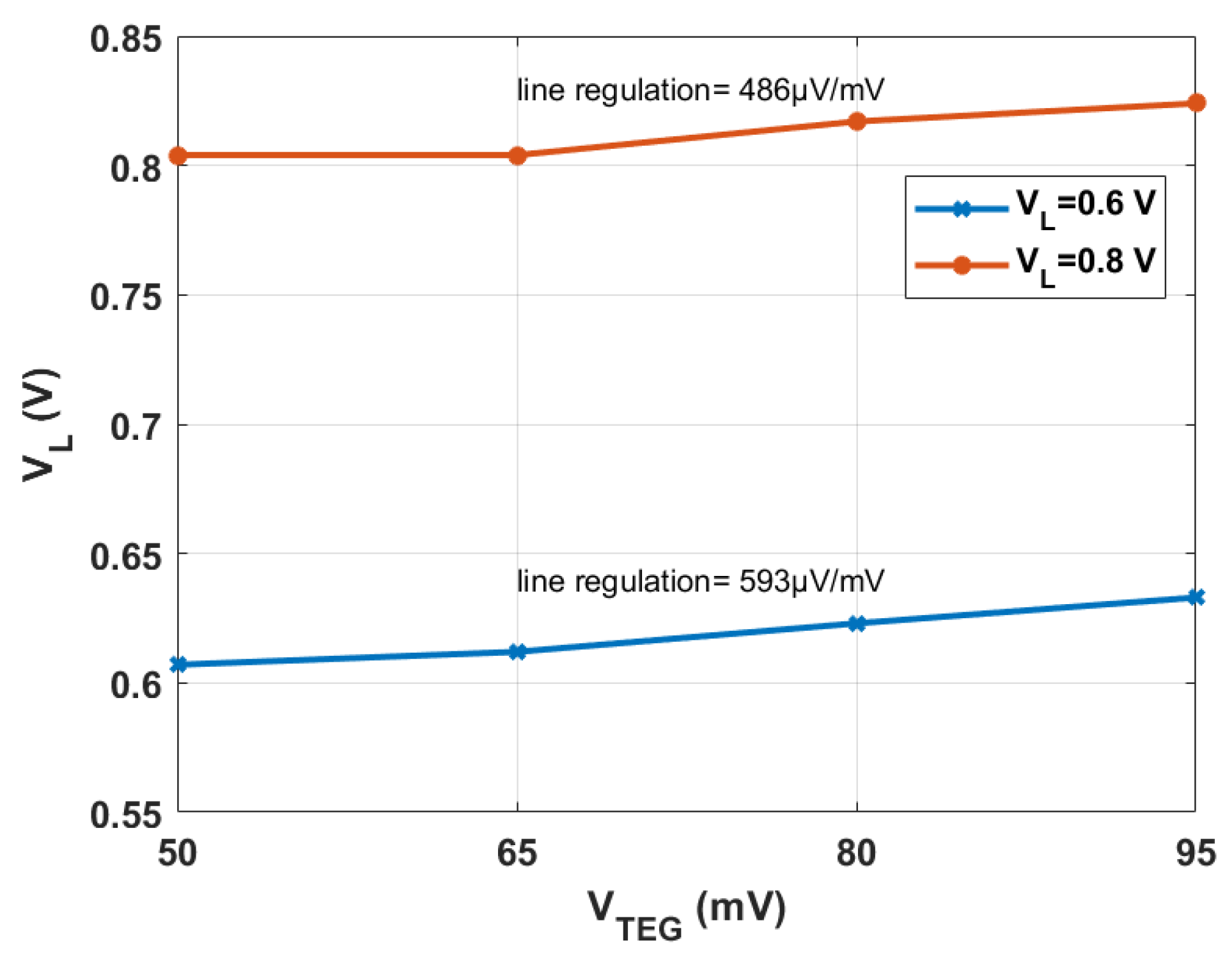
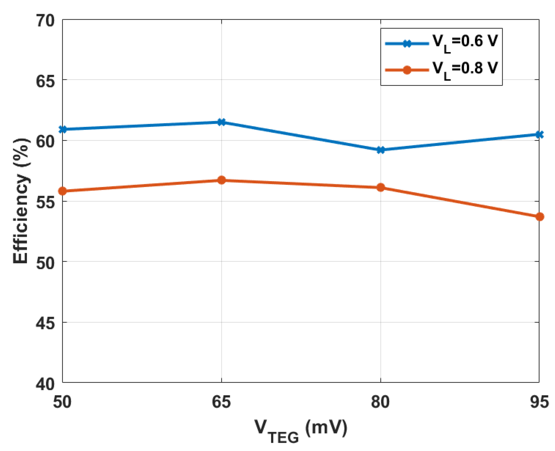
4. Simulation and Analysis in 65 nm CMOS Technology
5. Conclusions
Author Contributions
Funding
Institutional Review Board Statement
Informed Consent Statement
Data Availability Statement
Conflicts of Interest
References
- Radin, R.L.; Sawan, M.; Galup-Montoro, C.; Schneider, M.C. A 7.5-mV-Input Boost Converter for Thermal Energy Harvesting With 11-mV Self-Startup. IEEE Trans. Circuits Syst. II Express Briefs 2020, 67, 1379–1383. [Google Scholar] [CrossRef]
- Bose, S.; Anand, T.; Johnston, M.L. A 3.5-mV Input Single-Inductor Self-Starting Boost Converter With Loss-Aware MPPT for Efficient Autonomous Body-Heat Energy Harvesting. IEEE J. Solid-State Circuits 2021, 56, 1837–1848. [Google Scholar] [CrossRef] [PubMed]
- Luo, Z.; Zeng, L.; Lau, B.; Lian, Y.; Heng, C.H. A sub-10 mV power converter with fully integrated self-start, MPPT, and ZCS control for thermoelectric energy harvesting. IEEE Trans. Circuits Syst. I Regul. Pap. 2017, 65, 1744–1757. [Google Scholar] [CrossRef]
- Yu, H.; Chen, M.; Wu, C.; Tang, K.T.; Wang, G. A batteryless and single-inductor DC-DC boost converter for thermoelectric energy harvesting application with 190mV cold-start voltage. In Proceedings of the 2018 IEEE International Symposium on Circuits and Systems (ISCAS), Florence, Italy, 27–30 May 2018; pp. 1–4. [Google Scholar]
- Jhang, J.J.; Wu, H.H.; Hsu, T.; Wei, C.L. Design of a Boost DC–DC Converter With 82-mV Startup Voltage and Fully Built-in Startup Circuits for Harvesting Thermoelectric Energy. IEEE Solid-State Circuits Lett. 2020, 3, 54–57. [Google Scholar] [CrossRef]
- Lim, B.M.; Seo, J.I.; Lee, S.G. A colpitts oscillator-based self-starting boost converter for thermoelectric energy harvesting with 40-mV startup voltage and 75% maximum efficiency. IEEE J. Solid-State Circuits 2018, 53, 3293–3302. [Google Scholar] [CrossRef]
- Chen, M.; Yu, H.; Wang, G.; Lian, Y. A batteryless single-inductor boost converter with 190 mV self-startup voltage for thermal energy harvesting over a wide temperature range. IEEE Trans. Circuits Syst. II Express Briefs 2018, 66, 889–893. [Google Scholar] [CrossRef]
- Yoon, S.; Carreon-Bautista, S.; Sánchez-Sinencio, E. An area efficient thermal energy harvester with reconfigurable capacitor charge pump for IoT applications. IEEE Trans. Circuits Syst. II Express Briefs 2018, 65, 1974–1978. [Google Scholar] [CrossRef] [Green Version]
- Bose, S.; Anand, T.; Johnston, M.L. A 3.5 mv input, 82% peak efficiency boost converter with loss-optimized mppt and 50 mv integrated cold-start for thermoelectric energy harvesting. In Proceedings of the 2019 IEEE Custom Integrated Circuits Conference (CICC), Austin, TX, USA, 14–17 April 2019; pp. 1–4. [Google Scholar]
- Radin, R.L.; Sawan, M.; Schneider, M.C. An Accurate Zero-Current-Switching Circuit for Ultra-Low-Voltage Boost Converters. IEEE Trans. Circuits Syst. II Express Briefs 2020, 68, 1773–1777. [Google Scholar] [CrossRef]
- Alhawari, M.; Mohammad, B.; Saleh, H.; Ismail, M. An efficient zero current switching control for L-based DC–DC converters in TEG applications. IEEE Trans. Circuits Syst. II Express Briefs 2016, 64, 294–298. [Google Scholar] [CrossRef]
- El-Damak, D.; Chandrakasan, A.P. A 10 nW–1 μW power management IC with integrated battery management and self-startup for energy harvesting applications. IEEE J. Solid-State Circuits 2016, 51, 943–954. [Google Scholar]
- Carreon-Bautista, S.; Eladawy, A.; Mohieldin, A.N.; Sanchez-Sinencio, E. Boost converter with dynamic input impedance matching for energy harvesting with multi-array thermoelectric generators. IEEE Trans. Ind. Electron. 2014, 61, 5345–5353. [Google Scholar] [CrossRef]
- Huang, C.H.; Liao, W.C. A high-performance LDO regulator enabling low-power SoC with voltage scaling approaches. IEEE Trans. Very Large Scale Integr. VLSI Syst. 2020, 28, 1141–1149. [Google Scholar] [CrossRef]
- Liu, P.; Huang, S.; Duan, Q.; Zhu, Q.; Meng, Z. A Low-Quiescent Current Off-Chip Capacitor-less LDO Regulator with UGCC Compensation. In Proceedings of the 2019 IEEE International Conference on Electron Devices and Solid-State Circuits (EDSSC), Xi’an, China, 12–14 June 2019; pp. 1–3. [Google Scholar]
- Zhao, M.; Li, M.; Song, S.; Hu, Y.; Yao, Y.; Bai, X.; Hu, R.; Wu, X.; Tan, Z. An Ultra-Low Quiescent Current Tri-Mode DC-DC Buck Converter With 92.1% Peak Efficiency for IoT Applications. IEEE Trans. Circuits Syst. I Regul. Pap. 2021, 69, 428–439. [Google Scholar] [CrossRef]
- Santoro, F.; Kuhn, R.; Gibson, N.; Rasera, N.; Tost, T.; Graeb, H.; Wicht, B.; Brederlow, R. A hysteretic buck converter with 92.1% maximum efficiency designed for ultra-low power and fast wake-up SoC applications. IEEE J. Solid-State Circuits 2018, 53, 1856–1868. [Google Scholar] [CrossRef]
- Wang, Q.; Yang, P.; Jiang, H.; Guo, Y.; Jia, W.; Wang, Z. A 34 nA Quiescent Current Switched-Capacitor Step-Down Converter with 1.2 V Output Voltage and 0–5 μA Load Current. In Proceedings of the 2020 IEEE International Symposium on Circuits and Systems (ISCAS), Sevilla, Spain, 10–21 October 2020; pp. 1–5. [Google Scholar]
- Kilani, D.; Alhawari, M.; Mohammad, B.; Saleh, H.; Sanduleanu, M.; Ismail, M. Cascaded power management unit characterization for TEG-based IoT devices in 65 nm CMOS. Microelectron. J. 2019, 90, 285–296. [Google Scholar] [CrossRef]
- Alhawari, M.; Tekeste, T.; Mohammad, B.; Saleh, H.; Ismail, M. Power management unit for multi-source energy harvesting in wearable electronics. In Proceedings of the 2016 IEEE 59th International Midwest Symposium on Circuits and Systems (MWSCAS), Abu Dhabi, United Arab Emirates, 16–19 October 2016; pp. 1–4. [Google Scholar]
- Forghani-Zadeh, H.P.; Rincón-Mora, G.A. Low-power CMOS ramp generator circuit for DC-DC converters. J. Low Power Electron. 2006, 2, 437–441. [Google Scholar] [CrossRef] [Green Version]
- González, I.; Sánchez, A.; Langarica-Cordoba, D.; Yanine-Misleh, F.; Ramirez, V. A PI+ Sliding-Mode Controller Based on the Discontinuous Conduction Mode for an Unidirectional Buck–Boost Converter with Electric Vehicle Applications. Energies 2021, 14, 6785. [Google Scholar] [CrossRef]
- Wang, J.; Rong, J.; Yu, L. Dynamic prescribed performance sliding mode control for DC-DC buck converter system with mismatched time-varying disturbances. ISA Trans. 2022, in press. [Google Scholar] [CrossRef]
- Paidimarri, A.; Chandrakasan, A.P. A wide dynamic range buck converter with sub-nW quiescent power. IEEE J. Solid-State Circuits 2017, 52, 3119–3131. [Google Scholar] [CrossRef]
- Chen, N.; Wei, T.; Liu, J.; Jin, J.; Wei, X. A Digital Controller IC for High-Frequency DC-DC Switching Converters. In Proceedings of the 2019 14th IEEE Conference on Industrial Electronics and Applications (ICIEA), Xi’an, China, 19–21 June 2019; pp. 1645–1648. [Google Scholar]
- Qasem, L.; Kilani, D.; Mohammad, B.; Sanduleanu, M. Time-based Digital LDO Regulator. In Proceedings of the 31st International Conference on Microelectronics (ICM 2019), Cairo, Egypt, 15–18 December 2019; pp. 23–26. [Google Scholar]
- Kilani, D.; Alhawari, M.; Mohammad, B. L-based DC-DC Boost Regulator Using Voltage-to-Time Converter for Self-powered Devices. In Proceedings of the 2021 IEEE International Midwest Symposium on Circuits and Systems (MWSCAS), East Lansing, MI, USA, 8–11 August 2021; pp. 970–973. [Google Scholar]
- Yadav, N.; Kim, Y.; Alashi, M.; Ken Choi, K. Design of a Voltage to Time Converter with High Conversion Gain for Reliable and Secure Autonomous Vehicles. Electronics 2020, 9, 384. [Google Scholar] [CrossRef] [Green Version]
- Mostafa, H.; Ismail, Y.I. Highly-Linear Voltage-to-Time Converter (VTC) Circuit for Time-based Analog-to-Digital Converters (T-ADCs). In Proceedings of the IEEE 20th International Conference on Electronics, Circuits, and Systems (ICECS), Abu Dhabi, United Arab Emirates, 8–11 December 2013; pp. 149–152. [Google Scholar]
- Chen, Q.; Liang, Y.; Kim, B.; Boon, C.C. A 3GS/s Highly Linear Energy Efficient Constant-Slope Based Voltage-to-Time Converter. In Proceedings of the 2020 IEEE International Symposium on Circuits and Systems (ISCAS), Sevilla, Spain, 10–21 October 2020; pp. 1–5. [Google Scholar]
- Wahbah, M.; Alhawari, M.; Mohammad, B.; Saleh, H.; Ismail, M. Characterization of human body-based thermal and vibration energy harvesting for wearable devices. IEEE J. Emerg. Sel. Top. Circuits Syst. 2014, 4, 354–363. [Google Scholar] [CrossRef]


| (V) | 1.2 |
| (V) | 0–1 |
| (fF) | 200 |
| (fF) | 100 |
(nm/nm) | 600/60 |
| (nm/nm) | 200/60 |
| (nm/nm) | 250/140 |
| (nm/nm) | 200/60 |
| (m/nm) | 1/60 |
| (V) | 0.6 |
| (V) | 0.35 |
| Work | [30] | [28] | [29] | Proposed |
|---|---|---|---|---|
| Technique | constant slope | super MOS | starved inverter | sampling circuit |
| Technology (nm) | 65 | 45 | 65 | 65 |
(V) | 1 | 0.5 | 1 | 1.2 |
(V) | 0–1 | 0.1–0.5 | 0.2–0.35 | 0–1 |
| Linearity range | high 0–1 | low 0.2–0.4 | low 0.2–0.35 | high 0–1 |
| Gain (ns/V) | 0.144 | 101.43 | 3.47 | 11,500 |
| Power (W) | 8300 | - | - | 6.7 |
| MSE (s) | - | - | - | 2.04 × |
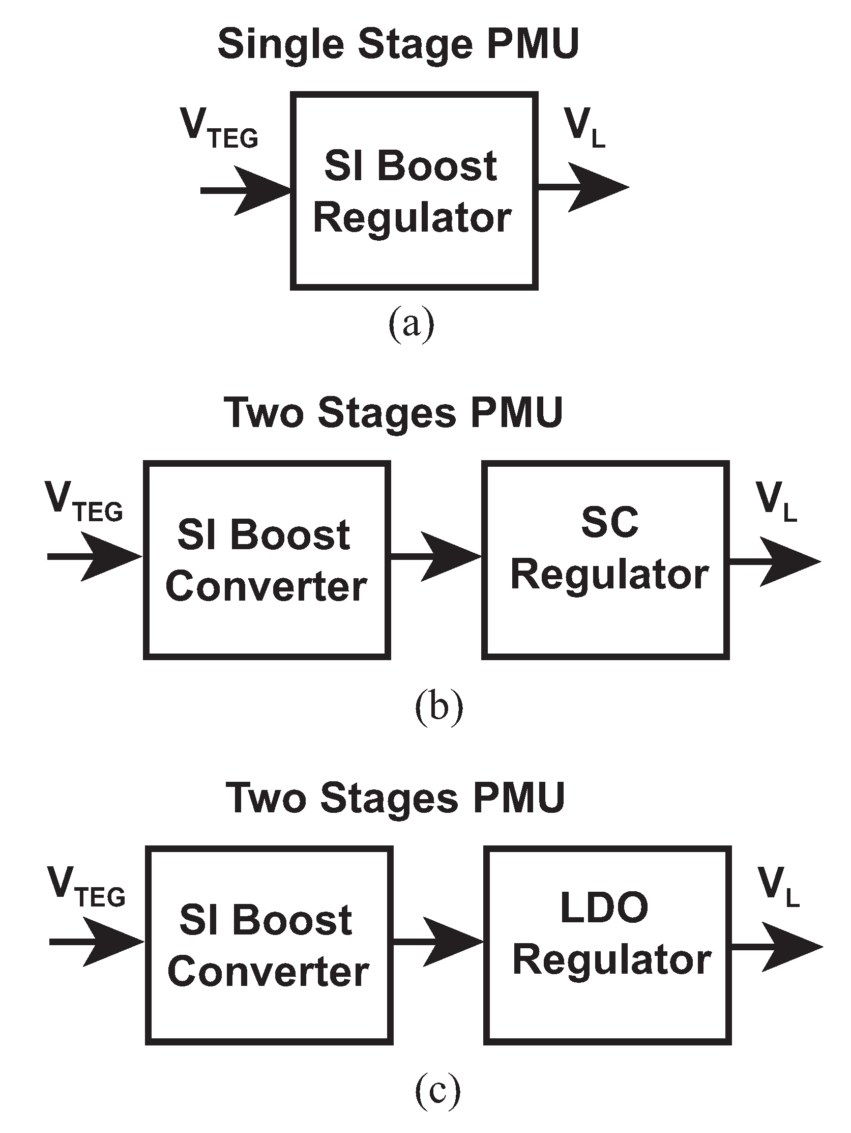
| Topology | SI + SC | SI + LDO | SI Regulator * |
|---|---|---|---|
| Technology (nm) | 65 | 65 | 65 |
(mV) | 50–65 | 50–65 | 50 |
| (V) | 0.6–0.8 | 0.6–0.8 | 0.6–0.8 |
| Voltage ripple (mV) | 35 | 12 | 25 |
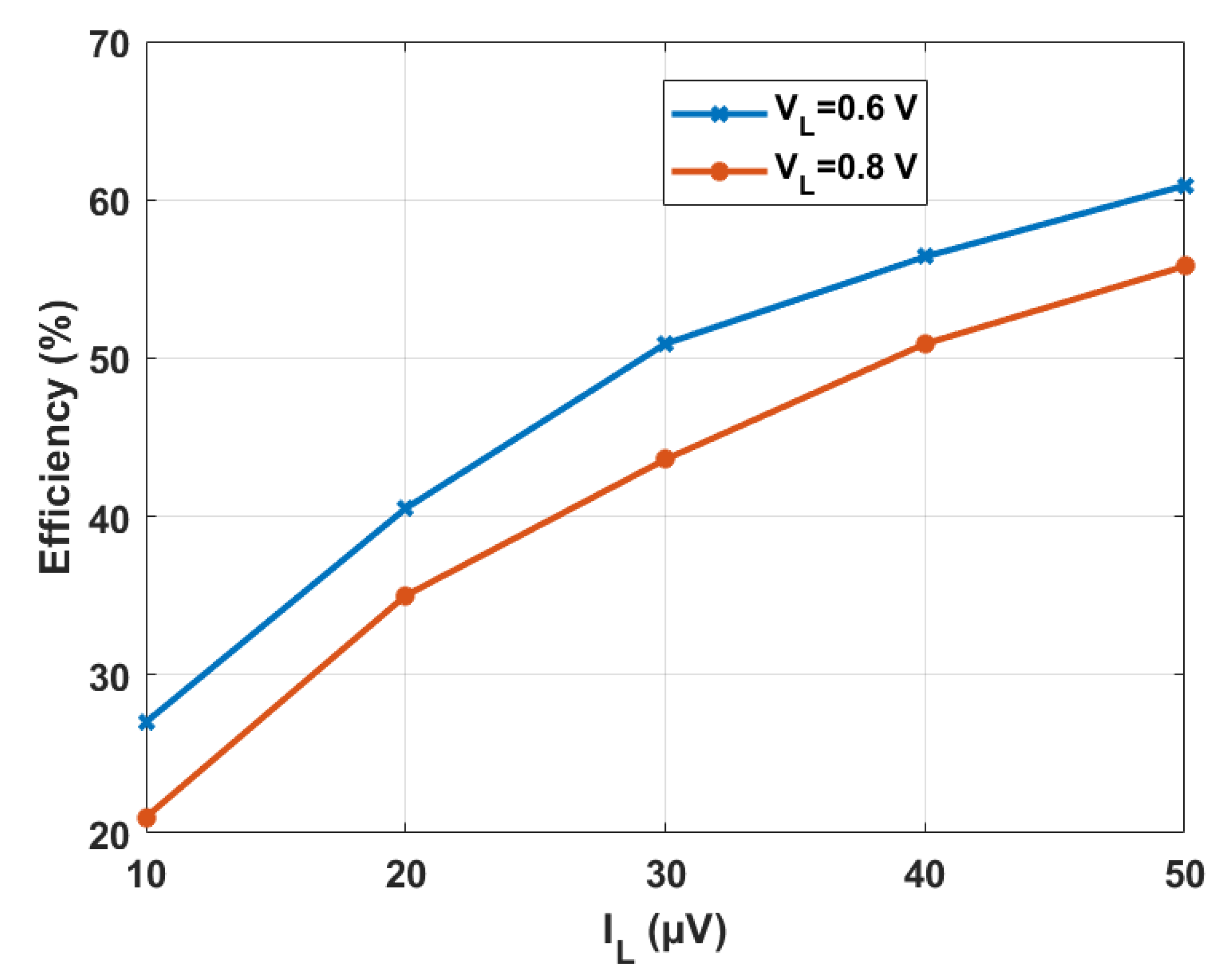
| Efficiency (%) @ = 10 A = 0.6 V | 10 | 9 | 27 |
| Efficiency (%) @ = 50 A = 0.6 V | 45 | 48 | 60.9 |
| Area (mm) | 0.531 | 0.0717 | 0.055 |
Publisher’s Note: MDPI stays neutral with regard to jurisdictional claims in published maps and institutional affiliations. |
© 2022 by the authors. Licensee MDPI, Basel, Switzerland. This article is an open access article distributed under the terms and conditions of the Creative Commons Attribution (CC BY) license (https://creativecommons.org/licenses/by/4.0/).
Share and Cite
Kilani, D.; Mohammad, B.; Alhawari, M. Switched Inductor DC–DC Boost Regulator Using Voltage-to-Time Controller for TEG Applications. Energies 2022, 15, 3330. https://doi.org/10.3390/en15093330
Kilani D, Mohammad B, Alhawari M. Switched Inductor DC–DC Boost Regulator Using Voltage-to-Time Controller for TEG Applications. Energies. 2022; 15(9):3330. https://doi.org/10.3390/en15093330
Chicago/Turabian StyleKilani, Dima, Baker Mohammad, and Mohammad Alhawari. 2022. "Switched Inductor DC–DC Boost Regulator Using Voltage-to-Time Controller for TEG Applications" Energies 15, no. 9: 3330. https://doi.org/10.3390/en15093330
APA StyleKilani, D., Mohammad, B., & Alhawari, M. (2022). Switched Inductor DC–DC Boost Regulator Using Voltage-to-Time Controller for TEG Applications. Energies, 15(9), 3330. https://doi.org/10.3390/en15093330