Article

A Resistor-Network Model of Dickson Charge Pump Using Steady-State Analysis

by
Abdullah S. Aloqlah
and
Mohammad Alhawari
*
Wayne Center for Integrated Circuits and Systems (WINCAS), Department of Electrical and Computer Engineering, Wayne State University, Detroit, MI 48202, USA
*
Author to whom correspondence should be addressed.
Energies 2022, 15(5), 1899; https://doi.org/10.3390/en15051899
Submission received: 3 February 2022 / Revised: 1 March 2022 / Accepted: 1 March 2022 / Published: 4 March 2022
(This article belongs to the Special Issue Energy Harvesting Circuits and Systems for Low-Power IoT Devices)

Abstract

:
This paper presents a new average behavioral model, named a resistor-network (RN) model, that accurately predicts the electrical characteristics of the Dickson charge pump (DCP) circuit in the slow-switching limit and the fast-switching limit regions based on steady-state analysis. The RN model describes the steady-state behavior of a single-stage DCP using a network of resistors, which can then be cascaded to model N-stage DCP, taking into account the top- and bottom-plate parasitic capacitances. The RN model provides a comprehensive insight into various design parameters of the DCP, including the input/output current, output voltage, load characteristics, losses caused by parasitics, and power efficiency. Simulation results show that the proposed RN model accurately predicts the output voltage and power efficiency of the DCP over a wide range of switching frequencies, from 0.1 Hz to 1 GHz, with an error of less than 2% at the maximum power efficiency. The RN model provides designers with a simple and effective model to design DCP quickly and efficiently for a broad spectrum of applications, including energy harvesting and flash memory applications.

1. Introduction

Dickson charge pump (DCP) circuits are widely used to boost an input DC voltage and support a high-voltage conversion ratio (VCR) for various applications, such as flash memory [1] and energy harvesting systems [2,3]. Unlike inductor-based boost converters [4,5], DCP can be integrated on-chip since it consists of switches and capacitors, as shown in Figure 1. The output voltage of N-stage DCP is illustrated in Equation (1) [6]:
V o = V i n + N V Φ N I L R o u t ,
where R o u t is the output resistance of the DCP, V i n is the input DC voltage, N is the number of stages which is equal to the number of fly capacitors (C), I L is the load current, and V ϕ is the high-voltage level of the clock, which typically has a voltage amplitude of V i n . A DCP circuit operates in two regions, slow-switching limit (SSL) or fast-switching limit (FSL). SSL occurs when the switching frequency, f s , is low, causing the amount of charge transferred by the capacitors to dominate the power losses of the DCP. In contrast, FSL occurs when f s is high, causing the switch ON-resistance to prevent the capacitors from completely transferring their charge each period, and thus dominating the power losses of the DCP [7].
Various models are reported in the literature that describe the behavior of the DCP in the SSL and FSL regions, [8,9,10,11,12,13], including the transformer model [9,11,12,14,15,16], the RC model [10,17,18,19], and the discrete-time model [13,20,21]. Figure 2a shows the transformer model, where G is the conductance that represents the losses from the top and bottom parasitic capacitances, (N + 1) is the VCR of the DCP at no-load, R p m p is the output resistance which represents the conduction and the charge transfer losses of the DCP, and C p m p is the self-capacitance of the DCP [11,14,15,16]. The transformer model can predict the electrical characteristics of the DCP, including input/output current and output voltage at low- and mid-frequency ranges [15,16]. However, the transformer model has multiple drawbacks; first, it fails to predict the behavior of the DCP at high frequencies due to inaccurate modeling of the losses caused by the bottom-plate parasitic capacitances. To explain, the value of G becomes large at high frequencies and, thus, the resistance ( 1 / G ) becomes low, which accurately predicts larger losses at high frequencies. However, as shown in Figure 2a, the model predicts that the VCR of the DCP remains (N + 1) at high frequencies, which is not true since the VCR starts to decrease due to large losses caused by the parasitics, eventually becoming unity. Second, the transformer model assumes the clock voltage level is equal to the input voltage level, lumped at the input terminal, V i n . Hence, the model does not support a different clock voltage level than the input voltage level. Further, implementing a feedback loop using the transformer model is not a straightforward task since the clock port does not exist in the model. Third, the transformer model does not provide an insight into the behavior of a single-stage DCP but rather models the overall N-stage DCP.
Figure 2b shows the RC model, where V m = 1 + [ N / ( 1 + a 1 ) ] V i n , C p m p = ( 1 + a 1 ) C f s / 3 , R p m p = T / [ C ( 1 + a 1 ) ] , and a 1 is the top parasitic capacitance ratio [17]. The RC model is originally designed to study the DCP dynamics, including rise time, and the effects of the parasitic capacitances on the output voltage and the load characteristics [22,23]. The RC model can only be used for the low-frequency range since the relationship between R p m p and f s takes a different approach at high frequencies, due to the effects of ON-resistances of the switches in the DCP. Moreover, the RC model cannot be used for maximum power transfer estimations since it only models the output side of the DCP. Finally, the voltage ( V m ) is modeled as a dependent voltage source and, thus, the RC model cannot be utilized to model a single-stage DCP but rather models the overall N-stage DCP [24].
On the other hand, the discrete-time model can accurately predict the output voltage of the DCP by modeling it in the z-domain [13,20,21]. The discrete-time model is commonly used for closed-loop regulation, system stability, and feedback control, which can be optimally designed and simulated in a shorter time than the actual switching circuit. However, the transfer function in the z-domain becomes complex as the number of stages in the DCP increases. Additionally, it does not take into account the effects of switches’ internal resistances. In other words, it reflects the behavior of DCP accurately in the low-frequency range.
In this paper, we present a new and simple resistor-network ( R N ) average behavioral model that accurately predicts the electrical characteristics of the DCP, including the input/output current, output voltage, load characteristics, losses caused by the top- and bottom-plate capacitances, and power efficiency. The proposed RN model inherits power conversion properties, as in the transformer model, and exhibits an accurate behavior in the transient and steady-state response, as in the RC model. Unlike the reported models, the RN model describes the behavior of a single-stage DCP and can be generalized to N-stage DCP. The RN model provides a comprehensive insight into various design parameters of the DCP, which will be useful for a broad spectrum of applications.
The following points summarize the novelty of the proposed RN model compared to the reported models in the literature:
  • Unlike the reported models, the RN model can describe the electrical characteristics of the DCP over the whole frequency range in the SSL and the FSL regions;
  • Unlike the reported models, the proposed model provides access to clock levels, switching frequency, and internal nodes between charge pump stages by modeling each stage individually and then cascading them to model N-stage DCP. Thus, the proposed model assists with studying the voltages and currents for each stage as well as the losses caused by the parasitic capacitances. Further, the model helps with exploring the impact of the feedback network on the behavior of the DCP, including stage modulation for maximum power transfer, and pulse frequency modulation;
  • Since the proposed model uses a linear resistive network, the computation speed is inevitably enhanced without extra complications;
  • The proposed model highlights the effects of both top- and bottom-plate parasitic capacitances and how they impact the power performance and the maximum power transfer of the DCP over the entire frequency range.
The remainder of the paper is organized as follows. Section 2 demonstrates the RN model derivations with a detailed analysis of the effects of switch ON-resistance and parasitic capacitances. Simulation results are presented in Section 3 to validate the RN model. Finally, Section 4 concludes the paper.

2. RN Model Derivation and Analysis

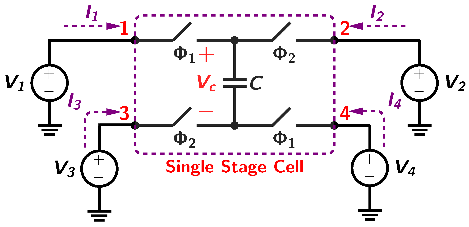
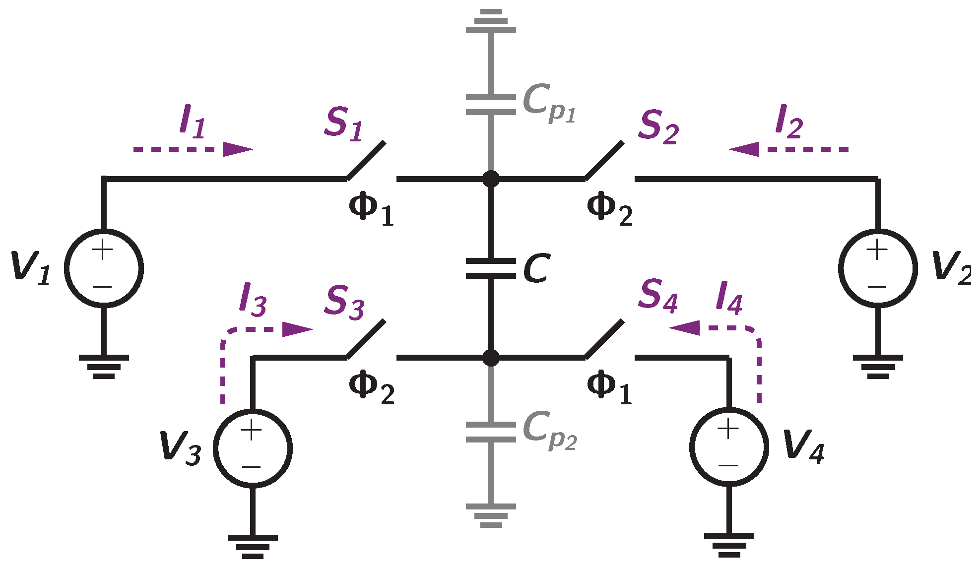
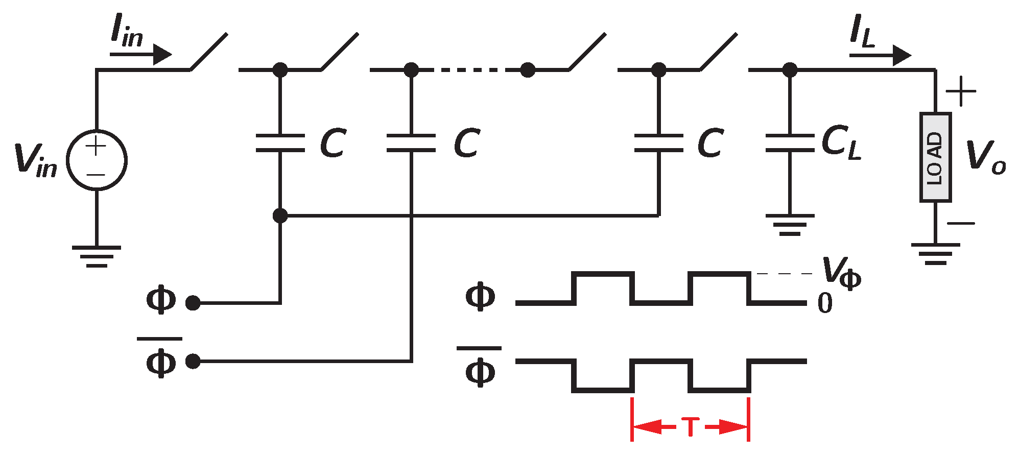
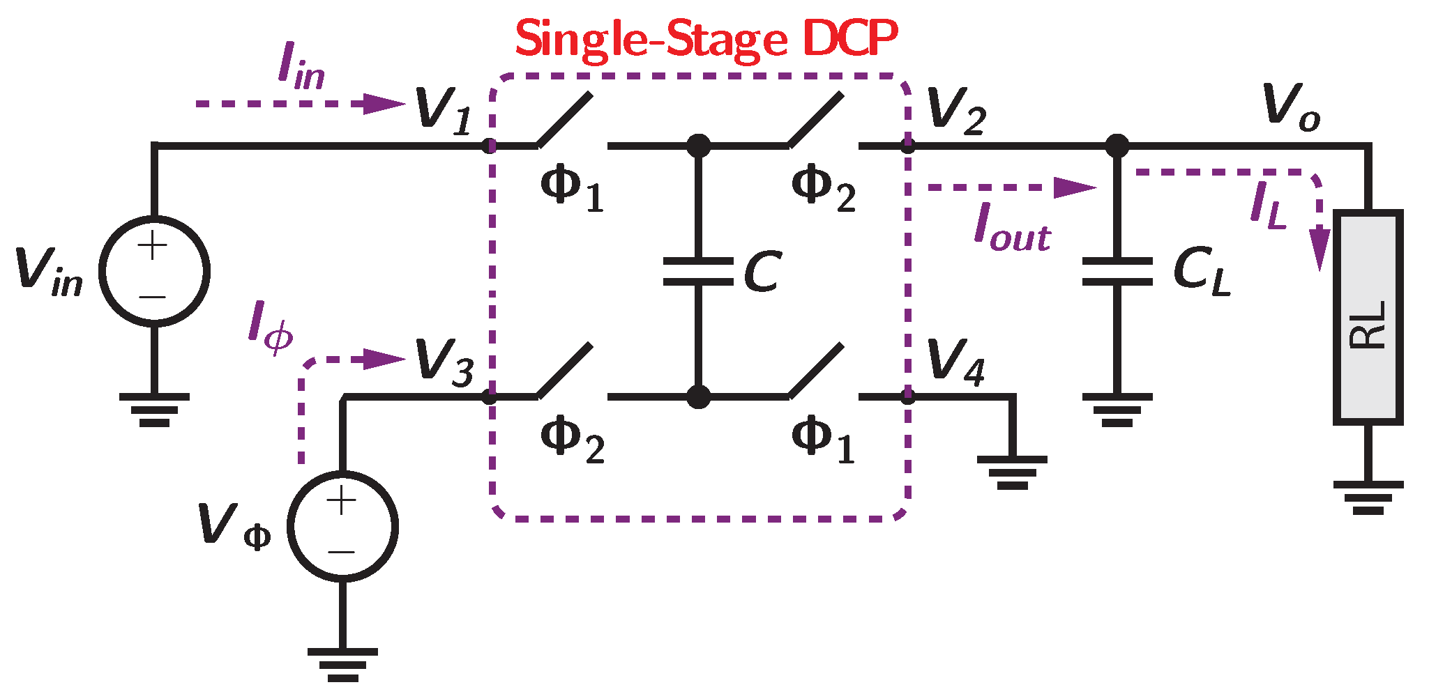
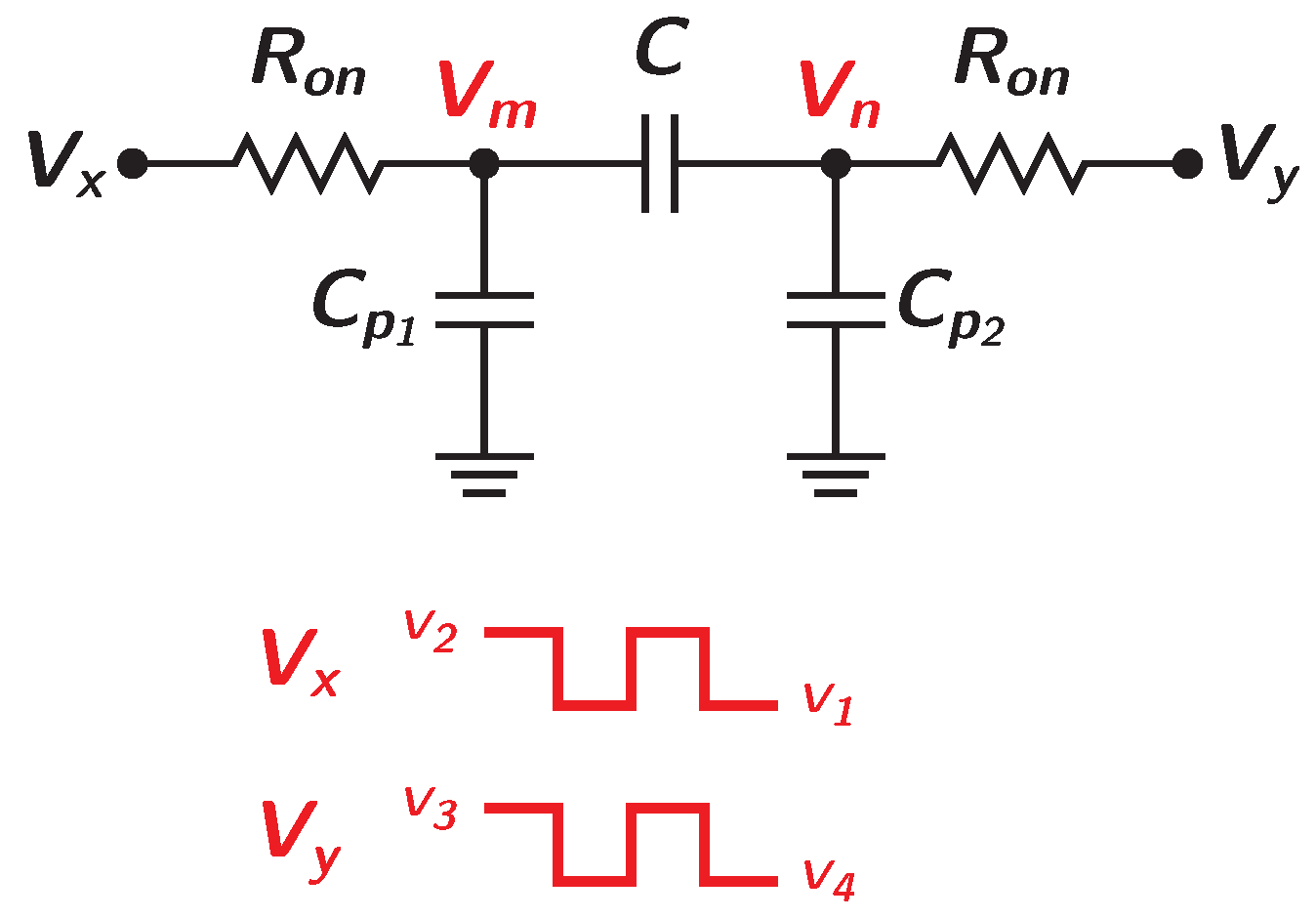
2.1. Single-Stage DCP Model Derivation

A single-stage DCP can be represented as a switching circuit, as in Figure 3, which consists of four switches with a fixed ON-resistance ( R o n ) and a fly capacitor (C), where the nodes V 1 , V 2 , V 3 , and V 4 reflect the input, output, and the clock high- and low-voltage levels, respectively.
Before modeling the DCP, it is essential to understand that the proposed model assumes the input variations are very slow compared to f s , the duty cycle of the clock is 50%, and all components (such as R o n ) in DCP are roughly fixed. We start modeling the DCP by analyzing a single-stage DCP, which can be replicated to model N-stage DCP. Figure 3 shows a single-stage DCP, which indicates the direction of the input and output currents.
To better analyze the DCP, Figure 4 shows a generic single-stage DCP. The average current, I 1 ¯ , that flows through the voltage source ( V 1 ) equals the total charge transferred to the fly capacitor, C, divided by the period, T, as shown in Equation (2a), and Equation (2b):
I 1 ¯ = Q n Q ( n 0.5 ) T = C ( V 1 V 4 ) C ( V 2 V 3 ) T ,
I 1 ¯ = C T ( V 1 V 2 + V 3 V 4 ) .
During Φ 1 , both V 1 and V 4 are in series; thus:
I 4 ¯ = I 1 ¯ = C ( V 1 V 4 ) C ( V 2 V 3 ) T = C T ( V 1 + V 2 V 3 + V 4 ) .
During Φ 2 , V 2 and V 3 are in series; thus:
I 2 ¯ = I 3 ¯ = C ( V 2 V 3 ) C ( V 1 V 4 ) T = C T ( V 1 V 2 + V 3 V 4 ) .
I 1 ¯ can be rewritten as a function of the terminal-to-terminal potential differences, such that:
I 1 ¯ = V 1 V 2 T / C + V 1 V 3 T / C + V 1 V 4 T / C = V 1 V 2 R + V 1 V 3 R + V 1 V 4 R .
The term ( T / C ) is defined as the equivalent switching resistance, R, which represents the energy loss that occurs every charge cycle, as shown in Equation (6):
R = T C .
I 2 ¯ , I 3 ¯ , and I 4 ¯ can be analyzed similarly, as shown in Equations (7)–(9), respectively:
I 2 ¯ = V 2 V 1 R + V 2 V 4 R + V 2 V 3 R = I 1 ¯ ,
I 3 ¯ = V 3 V 1 R + V 3 V 2 R + V 3 V 4 R ,
I 4 ¯ = V 4 V 1 R + V 4 V 3 R + V 4 V 2 R = I 3 ¯ .

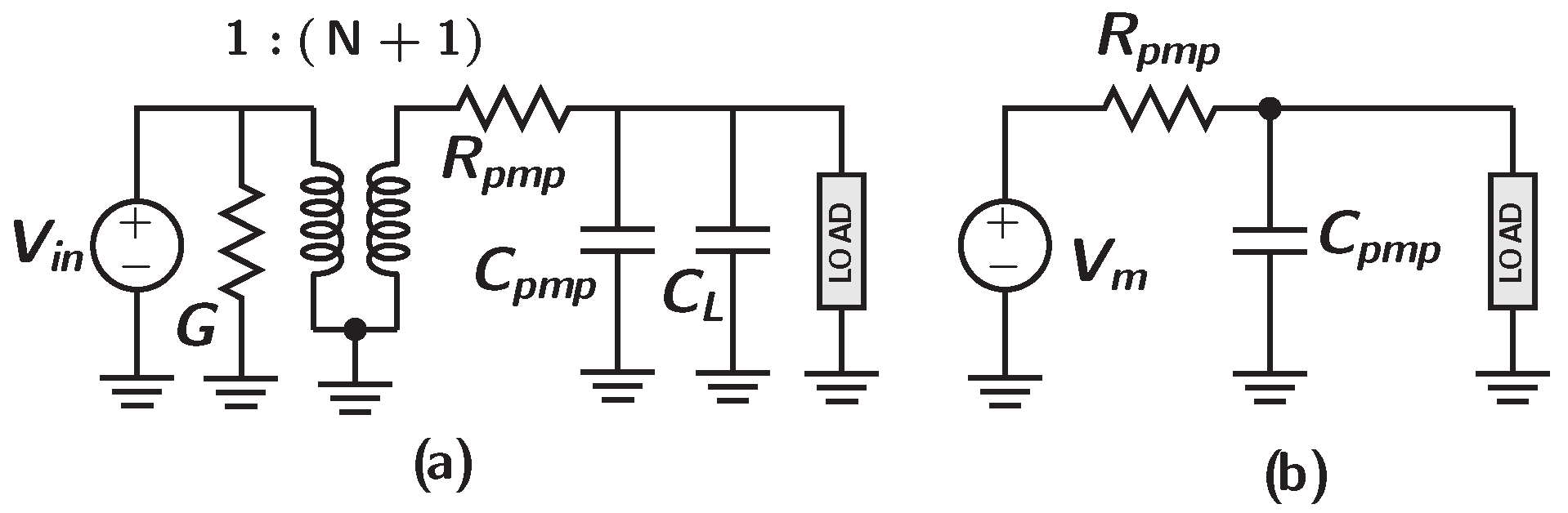
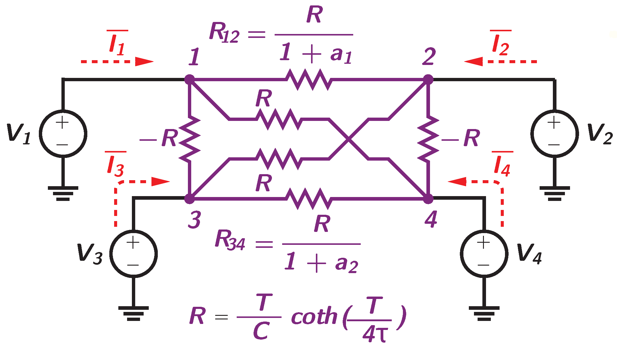
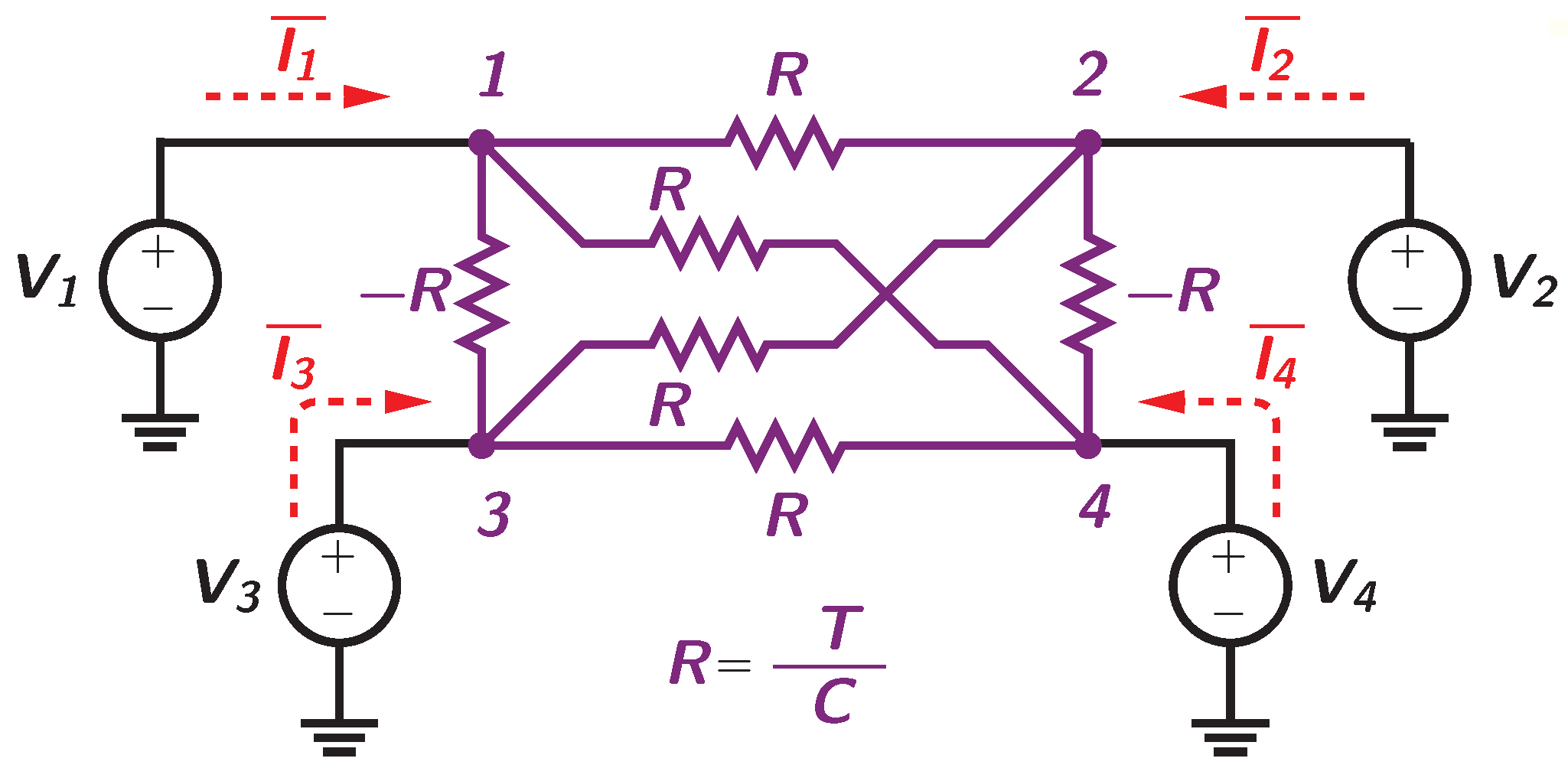
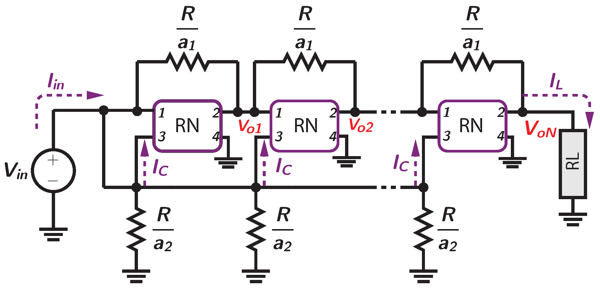
2.2. Proposed RN Model

Figure 5 presents the proposed RN model for a single-stage DCP, which consists of linear resistors connected between each terminal in the DCP according to Equations (5) and (7)–(9). All the resistances in Figure 5 are essential to describe the behavior of the DCP operation. The RN model in Figure 5 reveals key information regarding the behavior of a single-stage DCP. Namely, the resistor network, including the negative and positive resistances, entails two properties; voltage gain and power conversion. Furthermore, the RN model is symmetrical between the input and the output; however, the connection of input voltage sources on the left side in the actual circuit forces the power flow in a uni-directional path (from left to right). In addition, the RN model in Figure 5 describes the switching behavior of the DCP during SSL, when f s is low. Moreover, the equivalent output resistance seen between nodes 2 and 4 when V 1 and V 3 are zero is equal to R, which agrees with the equivalent switching resistance of a single-stage DCP shown in Equation (6). The resistor network in Figure 5 can be replicated N times in series to model N-stage DCP. As will be shown in Section 3, the RN model can be simulated using SPICE to characterize N-stage DCP, which will help researchers study various parameters of the DCP in a fast and accurate manner. The RN model in Figure 5 does not yet account for the switch ON-resistance and the parasitic capacitances and only accounts for the switching resistance of the DCP. As will be seen in the following subsections, when accounting for various parasitics, the RN model in Figure 5 stays the same; however, the value of R in the resistor network will be different to account for those parasitics. Note that there might be different circuit interpretations of Equations (5) and (7)–(9). However, we chose the circuit interpretation in Figure 5 for simplicity.
There is a key difference between the actual voltage and currents in the DCP circuit, as in Figure 3, compared to the calculated voltage and currents in the RN model, as in Figure 5. The voltage node in the DCP circuit alternates between two levels due to the charging and discharging of the flying capacitors. However, the voltage level estimated by the RN model is the average voltage of two consecutive nodes in the switching DCP. In contrast, the current estimated by the model at a certain time ( t 0 ) represents the average value of the corresponding current in the switching DCP during a time interval of (T) around t 0 .
Comparing the circuit in Figure 3 to the model in Figure 5, we have V 1 = V i n , V 3 = V Φ , V 2 = V o , and V 4 = 0 , while I 1 = I i n , I 2 = I o u t , and I 3 = I Φ . To calculate the power dissipation for a single-stage DCP, we first calculate the average input current based on Figure 3. The average input current ( I i n ¯ ),
I i n ¯ = I o u t ¯ = I 1 ¯ = I 2 ¯ = 1 R ( V i n V o + V Φ ) .
Since ( V 4 = 0 ), the output voltage is described as in Equation (10):
V o = V 2 = V i n + V Φ I o u t ¯ R .
The term ( V i n + V Φ ) represents the maximum available output voltage when the output current is zero (at the no-load condition).
The voltage ripple is considered an essential part of the output voltage. The ripple at high-frequency ranges ( f s > > ( R L C L ) 1 ) is negligible compared to the output voltage level. In contrast, at low- to mid-frequencies, the ripple can be derived by analyzing the last stage of the DCP at steady-state. Hence, the average charge delivered to the output capacitor, C L , equals to the average current flows through the load resistance, R L :
I L ¯ = C Δ V o T = V o R L .
Thus,
Δ V o = V o f s R L C L .
The average power dissipated, P D , due to charge transfer losses in a single-stage DCP is shown in Equation (12):
P D = V 1 I 1 ¯ + V 2 I 2 ¯ + V 3 I 3 ¯ + V 4 I 4 ¯ = V 1 I 1 ¯ + ( V 1 + V 3 + I 2 ¯ R ) I 2 ¯ + V 3 I 3 ¯ + 0 = I 2 ¯ 2 R = I o u t ¯ 2 R ,
where P D can be minimized by having a large fly capacitor or by increasing the switching frequency. However, as the switching frequency increases, the effects of R o n become dominant, as explained in the following subsection, and the resistance/frequency dependency takes a different approach.

2.3. The Effect of Switch ON-Resistance ( R o n )

The analysis in the previous subsection is valid during low-frequency ranges, i.e., the time constant of the charging/discharging paths, including R o n ; ( τ R o n C ) is very small compared to the half-cycle ( T / 2 ). Such preconditions guarantee that the fly capacitor will charge to ( V H = V 1 V 4 ) and discharge to ( V L = V 2 V 3 ). However, when f s increases, the time constant becomes comparable to the half-cycle and, thus, the DCP operates in the FSL. Therefore, the model and Equation (6) need to be modified to capture the effect of R o n , which can be achieved by using the same RN model in Figure 5 but deriving a different value for R. During SSL and based on Appendix A, which provides details on the steady-state analysis of a single-pole system, the fly capacitor will charge to ( V m a x ) and discharge to ( V m i n ), such that:
V m a x V m i n = ( V H V L ) tanh T 4 τ .
The average charge transfer to C is:
I 1 ¯ = C ( V m a x V m i n ) T = C tanh T 4 τ ( V H V L ) T = C T tanh T 4 τ ( V 1 V 4 V 2 + V 3 ) .
Thereby, the switching resistance, including the effect of R o n , is expressed in Equation (13):
R = 1 C f s coth 1 4 τ f s ,
where τ = 2 R o n C is the time constant of the charging/discharging paths. If f s is low, then the power loss is due to the charge transfer loss that happens due to the abrupt transition of the capacitors’ voltage levels [25], and the resistance curve is above the S S L asymptote line. Hence, as shown in Figure 6, the switching resistance is:
R = 1 C f s coth 1 4 τ f s 1 C f s .
In contrast, when f s is high, the power loss is due to the conduction losses in R o n , and the resistance curve is above the F S L asymptote line. Thus:
R = T C coth 1 4 τ f s T C × 4 τ f s = 4 τ C .
The corner frequency, f c , between the S S L and F S L frequencies is defined as the frequency at which the SSL and FSL asymptotes intersect, as demonstrated in Figure 6; thus:
f c = 1 4 τ .
Finally, the resistance estimated in Equation (13) describes the losses when the fly capacitor is charging and discharging through an ideal source, with symmetrical charge/discharge paths. In the first stage of the DCP, the charging path time constant is ( 2 R o n C ), while the discharging path is ( 1.5 R o n C ). For intermediate stages, both the charging time constant ( τ c ) and discharging time constant ( τ d ) are ( 1.5 R o n C ), and for the last stage, the time constants are ( 1.5 R o n C ) and ( 2 R o n C C L / ( C + C L ) ). In such a case, and as shown in Appendix B, the equivalent resistance of the DCP when considering non-symmetrical charging/discharging paths is:
R = 1 e T 2 τ c e T 2 τ d 1 e T 2 τ c + e T 2 τ d + + e T 2 τ c e T 2 τ d × T C ,
where Equation (16) shows that the resistance in the SSL range stays the same ( T / C ). This is expected since the resistance value of the charging and discharging paths does not impact the amount of losses due to charge sharing. In contrast, Equation (16) shows that the resistance in the FSL range is:
R 4 τ c + τ d 2 C = 4 τ a v g C = 2 R T ,
where R T is the sum of all R o n in a single DCP stage (i.e., R T = 4 R o n ), which is consistent with the result presented in [26]. In this case, we can approximate the effective time constant to be the average of the charging and discharging time constants. For instance, ignoring the series resistance of the input source ( R s ), in the first stage, the effective time constant is 0.5 ( 2 R o n C + 1.5 R o n C ) = 1.75 R o n C . Equation (16) reveals that the capacitance is not scaled to ( C / 2 ). Intuitively, even though the capacitance value is reduced by half, the equivalent resistance is doubled. However, the ripple on the fly capacitor shrinks with the same factor due to capacitance–voltage division. Thus, the charging and discharging from and into a capacitive load does not impact the equivalent resistance of the switching circuit unit in both SSL and FSL ranges. However, there is some error around the corner frequency which depends on the τ d / τ c .
For simplicity, Equation (13) can be still utilized, instead of Equation (16), by setting the time constant to be the effective time constant τ a v g , and keeping R and C the same. For example, when ( τ d = 0.75 τ c ), such approximation can yield a maximum error of 0.4% in resistance value, as shown in Figure 7. Therefore, the effect of R o n can be captured in the RN model by using the same resistor network in Figure 5, but using the equation of R in Equation (13).

2.4. The Effect of Parasitic Capacitance ( C p )

In this subsection, we will modify the RN model to include the effect of the parasitic capacitances and, thus, capture the behavior of the DCP during SSL and mid-frequency in the FSL. Again, the same RN model in Figure 5 will be used while deriving different values for the resistors. We will denote this model as the RN model with parasitic, or the RN-P model.
As f s increases, parasitic capacitors dominate the power losses in the DCP. As shown in Figure 8, two main parasitic capacitors, C p 1 and C p 2 , exist in a single-stage DCP. To include the impacts of C p 1 and C p 2 , we perform a similar analysis in Section 2.1 on the DCP shown in Figure 8. We define C p 1 and C p 2 as a percentage of the fly capacitor, C, such that C p 1 = a 1 C and C p 2 = a 2 C , where a 1 and a 2 are less than 1 and they depend on the CMOS technology node, the area of the fly capacitor, the metal layers used, the type of the capacitor (MIM, MOS, and MOM), and the layout design. To estimate a 1 and a 2 , a post-layout simulation can be used to extract the parasitic at each node. Experimentally, we can estimate the average value of a 1 and a 2 by measuring the input current and the output voltage at zero-load current, as will be shown in the next subsections.
During Φ 1 , the charge rate transferred through S 1 is:
I 1 ¯ = C T ( ( V 1 V 4 ) ( V 2 V 3 ) ) + C p 1 T ( V 1 V 2 ) = C T ( ( 1 + a 1 ) V 1 ( 1 + a 1 ) V 2 + V 3 V 4 ) = C T ( ( 1 + a 1 ) ( V 1 V 2 ) ( V 1 V 3 ) + ( V 1 V 4 ) ) .
Similarly, during Φ 2 , the charge rate transferred through S 3 is:
I 3 ¯ = C T ( ( V 3 V 2 ) ( V 1 V 4 ) ) + C p 2 T V 3 = C T ( V 1 V 2 + ( 1 + a 2 ) V 3 + V 4 ) .
Based on Equations (18) and (19), Figure 9 shows the RN-P model with amended R 12 and R 34 , which includes the effect of C p 1 and C p 2 , respectively, such that:
R 12 = R 1 + a 1 = R | | R a 1 R 34 = R 1 + a 2 = R | | R a 2 ,
where R is the same as was shown in Equation (13). As depicted in Figure 9, the effect of the C p 1 and C p 2 is reflected on R 12 and R 34 , respectively. Since R 12 and R 34 can be each seen as two parallel resistors, the RN-P model can be drawn as in Figure 10, which reveals key information regarding the effect of C p 1 and C p 2 . As depicted in Figure 10, as f s increases, the output voltage due to C p 1 decreases. However, since the term ( R / a 1 ) decreases, the total output resistance decreases. In contrast, as f s increases, the effect of C p 2 increases the power losses and does not affect the output voltage or the output current of the DCP. The impact of C p 1 and C p 2 in Figure 10 can be intuitively confirmed using Figure 8 as follows. During Φ 1 , C p 1 is charged to V 1 , while in Φ 2 , C p 1 is discharged to the output load, which confirms the direct contribution of C p 1 on the output voltage. In contrast, during Φ 2 , C p 2 is charged to V 3 , while in Φ 1 , C p 2 is discharged through V 4 , which is ground, and thus C p 2 does not impact the output voltage but rather the power losses. Note that the new represented form of the RN-P model in Figure 9 and Figure 10 makes the analysis of power loss, output resistance, and voltage level a straightforward task.
Based on Figure 10, the output voltage under zero load condition, I ¯ L = 0 A I ¯ C = I ¯ f 1 :
V o ( I L = 0 ) = V i n + V Φ I C R = V i n + V Φ V o V i n R / a 1 R ,
V o ( I L = 0 ) = V i n + V Φ 1 + a 1 .
The equivalent output resistance, R o u t , can be derived from the load characteristics equation:
V o = V i n + V Φ I L + V o V i n R / a 1 R = V i n + V Φ a 1 V o V i n + I L R               V o = V i n + V Φ 1 + a 1 R 1 + a 1 I L ,
R o u t = R 12 = R 1 + a 1 .
The feedback current I f 1 can be calculated as:
I f 1 = V o V i n R / a 1 = V i n + V Φ 1 + a 1 R 1 + a 1 I L V i n R / a 1 ,
I f 1 = a 1 1 + a 1 V Φ R I L .
The feedback current I f 2 can be calculated as:
I f 2 = a 2 V Φ R .
The charge pump current I C , at any I L , can be calculated as:
I C = I L + a 1 1 + a 1 V Φ R I L = a 1 1 + a 1 V Φ R + I L a 1 .
The power losses are equal to:
P D = I f 1 2 R a 1 + ( I L + I f 1 ) 2 R + a 2 V Φ 2 R .
Figure 11 shows the RN-P model, as in Figure 10, when cascaded N times to model the behavior of a N-stage DCP. As shown in Figure 11, the RN-P model for a single-stage DCP can be extended to N-stage DCP, which helps with having better insight on individual stages. Furthermore, since the RN-P model consists of only resistors, the simulation of DCP will be much faster than the switching DCP circuit, which will help designers optimize their circuits quickly.
Now, the DCP in Figure 11 can be analyzed, where the output voltage at no-load condition, ( I L = 0 A ) is:
V o 1 = V 1 + V 1 1 + a 1 = 1 + 1 1 + a 1 V i n ,
V o 2 = V o 1 + V 1 1 + a 1 = 1 + 2 1 + a 1 V i n .
Thus,
V o N = 1 + N 1 + a 1 V i n .
The output resistance of the DCP can be derived as:
R o u t = N R 1 + a 1 .
The result in Equations (27) and (28) are consistent with the equations first derived by Dickson ( V D = 0 volt, I o u t = 0 A, and a 1 = C s / C ) [27] and other work reported in the literature [7,26].

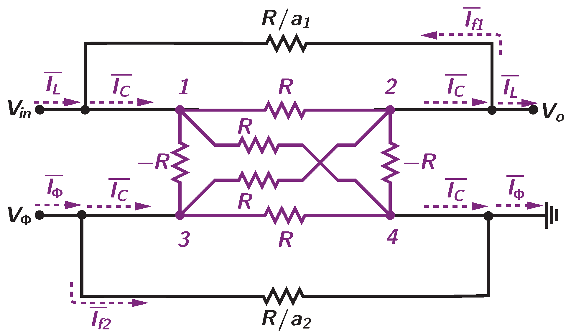
2.5. Maximum Power Transfer Methodologies

In energy harvesting applications, maximum power transfer is essential to maximize the extracted power and deliver the maximum power to the load [28,29,30,31]. The proposed RN model helps with deriving the output resistance of the DCP to achieve maximum power at the load for an input source, V s , with a source resistance R s . Equation (28) does not consider the effect of R s . Thus, the output resistance of the DCP, when including R s , can be expressed as [29]:
R o u t = N + 1 + a 1 1 + a 1 2 R s | | ( 1 + a 1 ) R ( a 1 + a 2 + a 1 a 2 ) N + N R 1 + a 1 .
If the load voltage is unregulated, then the optimum DCP resistance associated with maximum power delivered to a distinct N can be expressed as [29]:
R = ( a 1 + a 2 + a 1 a 2 ) R s R L ,
where ( R s > 0 ). The optimum resistance shown in Equation (30) is independent of N since it is defined as the resistance for the maximum power at the load and not the maximum available power delivered from the source. Note that, for a 1 = 0 , a 2 = 0 , the input impedance R I N = and R o u t = R = T / C . In this case, as R approaches zero, the power delivered to the load increases since the load voltage increases.
For regulated output voltage, the optimum DCP resistance can be expressed as [29]:
R R s N V o ( a 1 + a 2 ) V s ( N + 1 ) V o + ( N + 1 ) V o ( a 1 + a 2 ) ( V s ( N + 1 ) V o ) V s ( N + 1 ) V o ,
where ( R s > 0 ). Equations (30) and (31) reveal key information regarding maximum power transfer methodologies in the DCP circuit. When the output voltage is not regulated, the optimum resistance of the DCP is independent of N, as in Equation (30), and thus, stage modulation can be used to change N such that the input voltage of the DCP is equal to V s / 2 . For regulated output voltage, the optimum resistance of the DCP is a function of N, as in Equation (31). Therefore, both R and N need to be changed iteratively until reaching the optimum set of N o p t , R o p t .

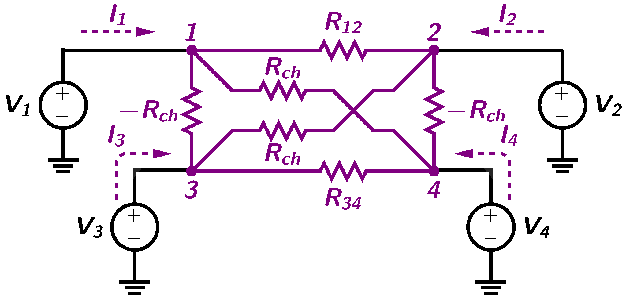
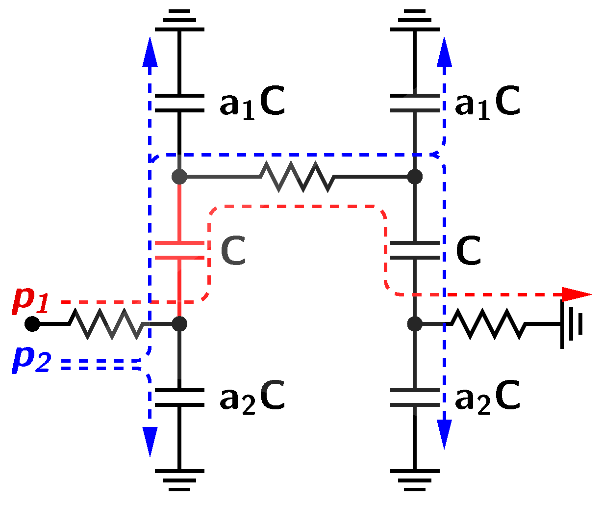
2.6. Generalization of RN Model

The RN-P model demonstrated in Figure 9 provides an accurate description of DCP at low frequencies (SSL) and the beginning of FSL, which is helpful for describing DCP in most applications. However, when the frequency becomes very high in FSL, the RN-P model does not capture the increase of the output resistance and the switching losses. Therefore, to have a complete insight into the behavior of DCP at the whole range of f s , an exact analysis of the RC circuit should be performed to understand the effects of parasitic losses. Thus, we denote this general model as the RN-G model. All details about the RN-G model analysis are included in Appendix C. The final RN-G model is shown in Figure 12, and the derivations are summarized in the following equations:
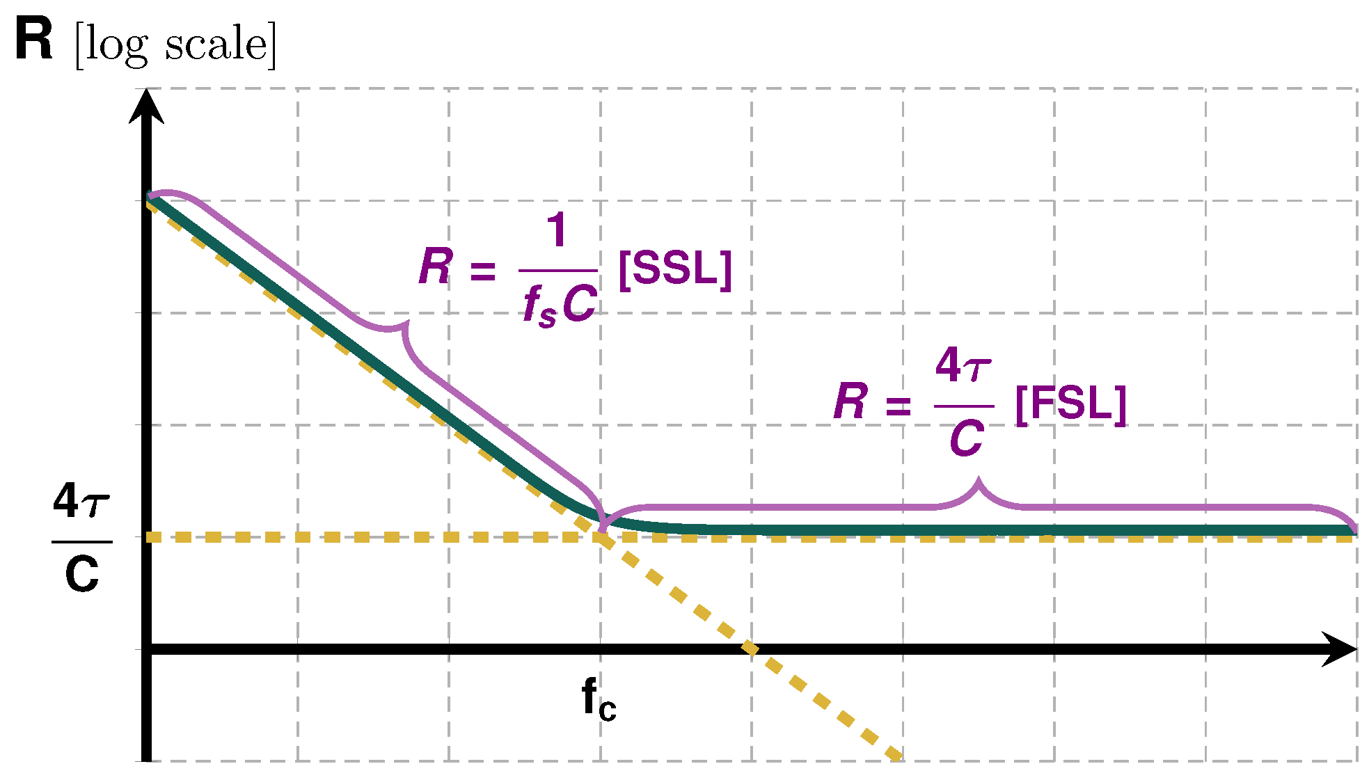
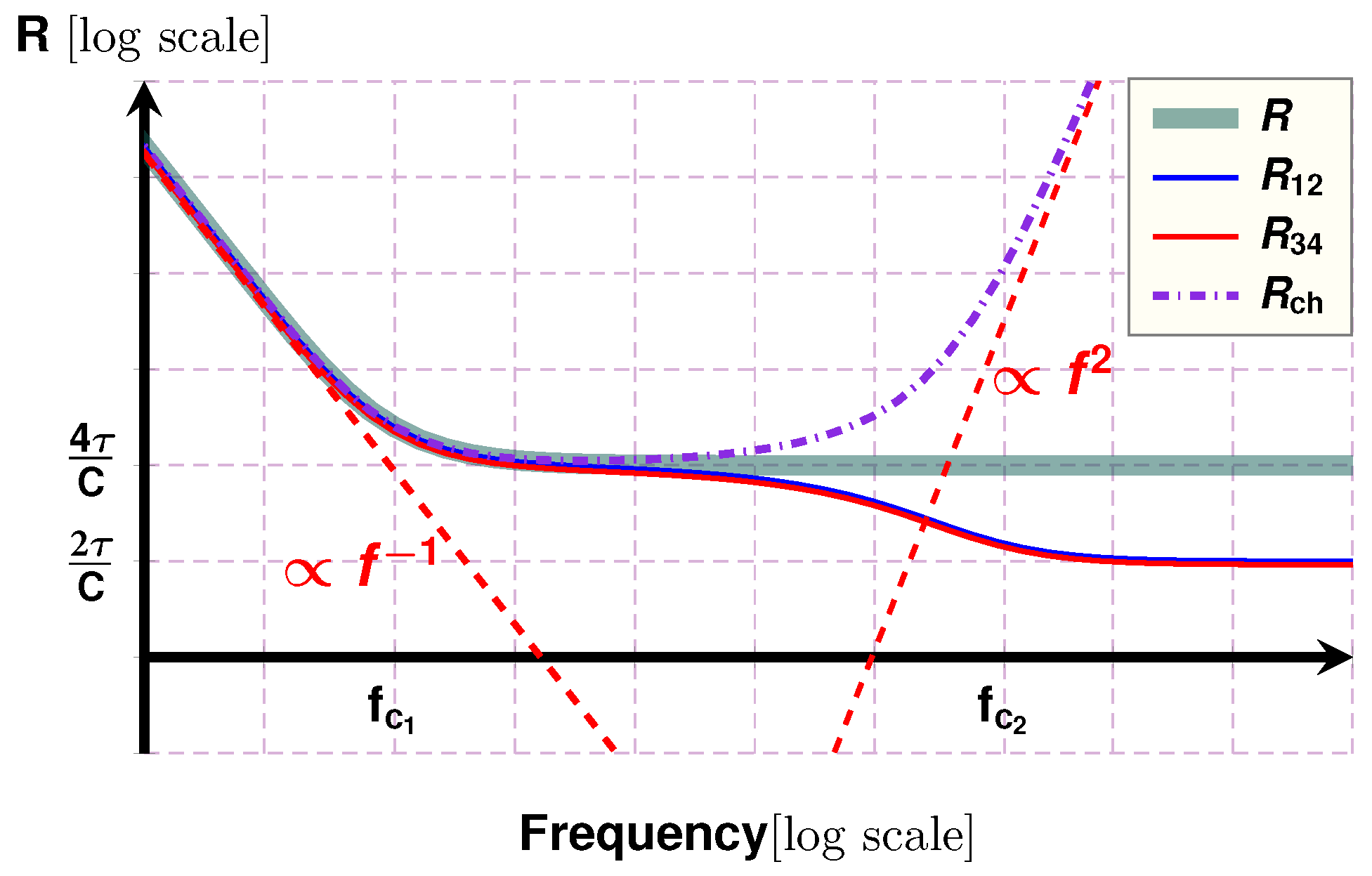
  • The circuit in Figure 8 has two distinct real poles:
    τ 1 2 + a 1 + a 2 2 R o n C , τ 2 a 1 + a 2 2 R o n C .
    Note that τ 2 is much smaller than τ 1 , and therefore, the second corner frequency, f c 2 , is much larger than the first corner frequency, f c 1 ;
  • The resistor between terminals 1 and 2, R 12 , can be expressed as a combination of two parallel resistors R 12 , 1 , and R 12 , 2 :
    R 12 = R 12 , 1 | | R 12 , 2 = 1 G 12 , 1 + G 12 , 2 ,
    where:
    G 12 , 1 = τ 1 ( 1 + a 2 ) R o n C τ 1 τ 2 τ 1 T R o n tanh T 4 τ 1 , G 12 , 2 = ( 1 + a 2 ) R o n C τ 2 τ 1 τ 2 τ 2 T R o n tanh T 4 τ 2 ;
  • Similarly, the resistor between terminals 3 and 4, R 34 , is a combination of two parallel resistors ( R 34 , 1 and R 34 , 2 ):
    R 34 = R 34 , 1 | | R 34 , 2 = 1 G 34 , 1 + G 34 , 2 ,
    where:
    G 34 , 1 = τ 1 ( 1 + a 1 ) R o n C τ 1 τ 2 τ 1 T R o n tanh T 4 τ 1 , G 34 , 2 = ( 1 + a 1 ) R o n C τ 2 τ 1 τ 2 τ 2 T R o n tanh T 4 τ 2 ;
  • The other four resistors, denoted as R c h in the RN-G model, can be calculated as:
    R c h = R 14 = R 23 = R 13 = R 24 = 1 G 1 + G 2 ,
    where:
    G 1 = τ 1 ( τ 1 τ 2 ) C T tanh T 4 τ 1 , G 2 = τ 2 ( τ 1 τ 2 ) C T tanh T 4 τ 2 .
At low-frequency ranges in the RN-G model, G 1 + G 2 C / T , R 12 = T / ( ( 1 + a 1 ) C ) , and R 34 = T / ( ( 1 + a 2 ) C ) , which matches the RN-P model in Figure 10. At high-frequency ranges, R c h = R 14 = R 23 = R 13 = R 24 = , and R 12 R 34 4 R o n .
Figure 12 and Figure 13 exhibit the RN-G schematic and summarize the model equivalent characteristics of a single-stage DCP at low-, mid-, and high-frequency ranges, where R 12 , R 34 , and R c h are plotted. The R graph, as in Equation (13), which includes the effect of R o n , is plotted for reference. At low frequencies, f < 1 / 4 τ 1 , the curve, R, follows the asymptotic lines, R = 1 / ( f s C ) , which demonstrates the equivalent resistance of a single-stage DCP with no parasitic effect. However, the curve, R, becomes equal to 8 R o n at high-frequency ranges where the ON-resistance effects are predominant. The curves R 12 , R 34 , and R c h have a second corner frequency at ( 1 / 4 τ 2 ) due to parasitic effects. At high-frequency ranges, R 12 R 34 4 R o n , and R c h = R 14 = R 32 = R 13 = R 24 increase in proportion to f 2 .
Finally, the time constants estimated in Equation (32) are based on symmetrical charging/discharging paths and assume a time constant of 2 R o n C . This assumption is not valid for our case of DCP. For instance, the charging path for the intermediate stages includes three resistors and two fly capacitors, as illustrated in Figure 14.
Where the first path ( p 1 ) has a time constant:
τ 1 3 2 R o n C ,
and the second time constant is obtained by shortening the fly capacitors and estimating the poles from the admittance formula. Thus:
τ 2 4 ( a 1 + a 2 ) 3 R o n C .
Similar formulas are valid for the discharging phase of the first stage and the charging phase of the last stage. However, for the first stage, and during the charging phase:
τ 1 2 R o n + R s C , τ 2 a 1 + a 2 2 R o n C ,
and for the last stage, during the discharging phase:
τ 1 2 R o n C C L C + C L 2 R o n C , τ 2 a 1 + a 2 2 R o n C .
As a final step, we model each stage based on the average values of τ 1 and τ 2 during the charging and discharging phases.

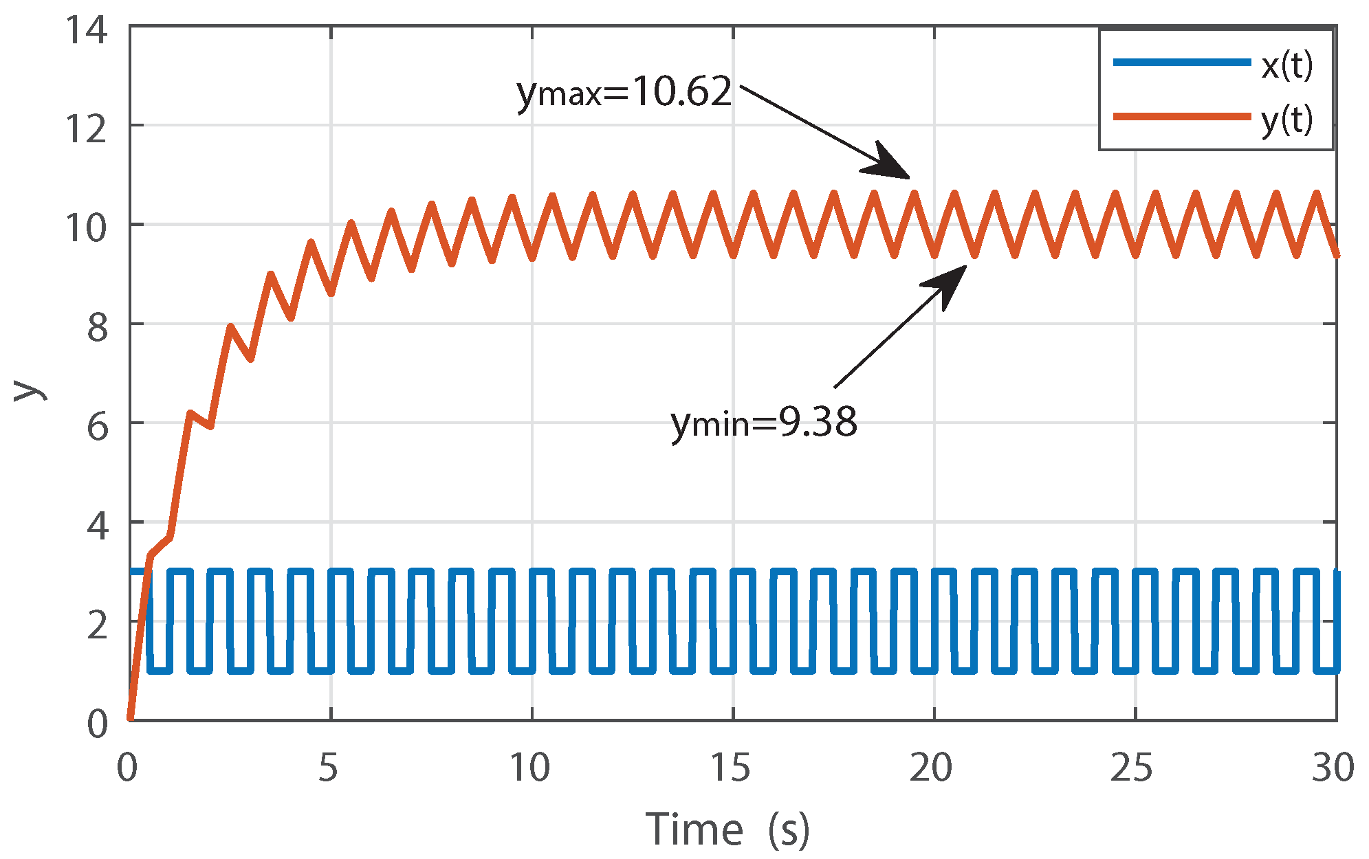
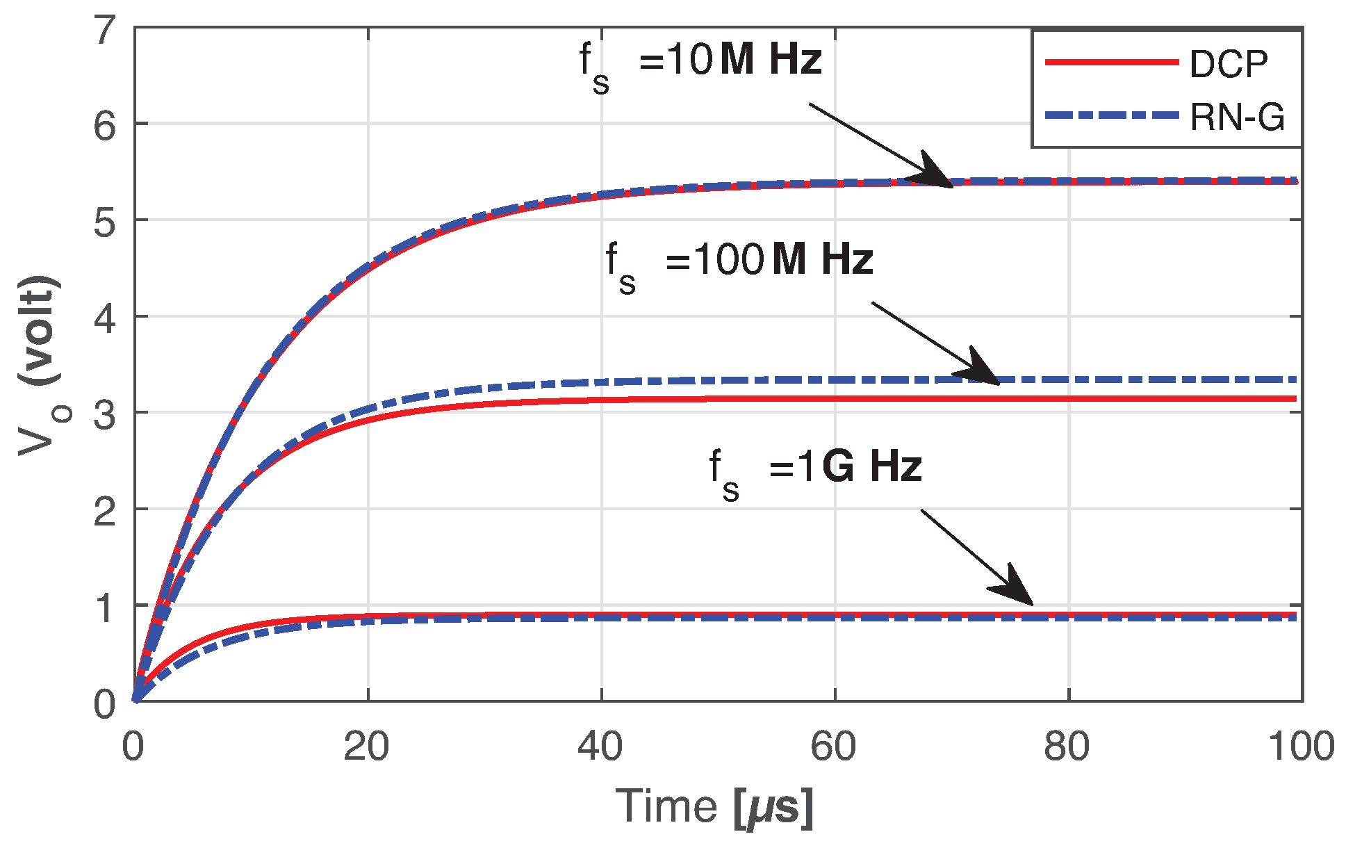
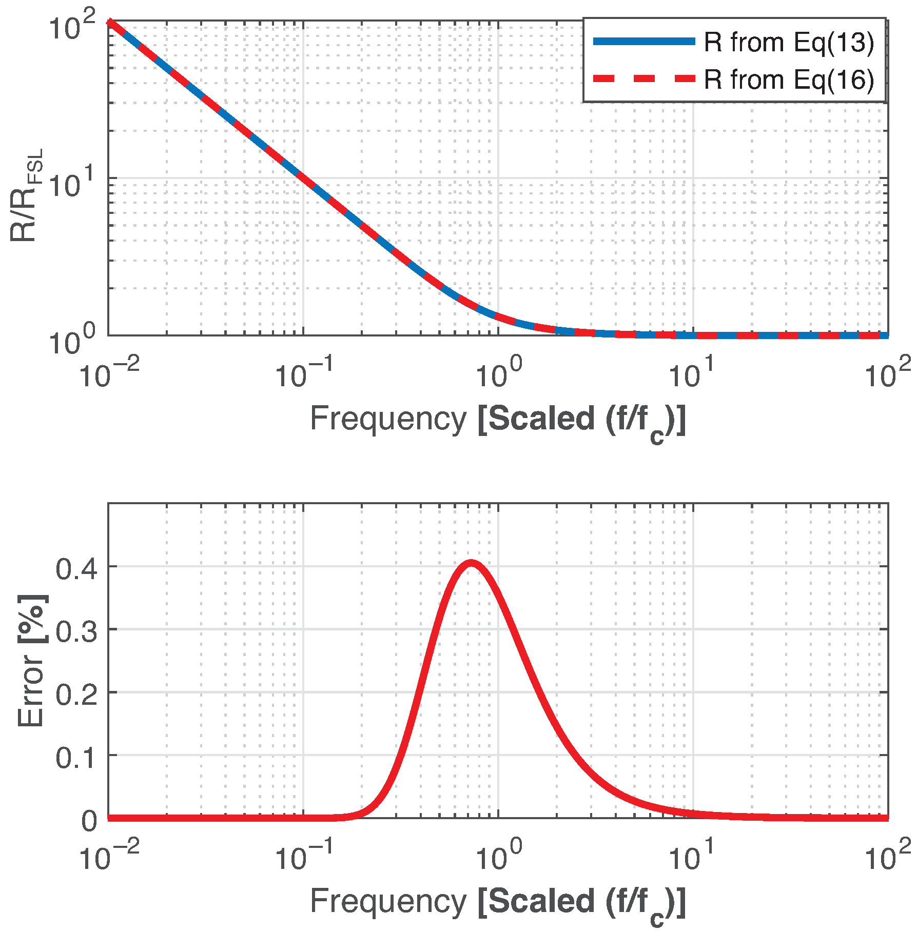
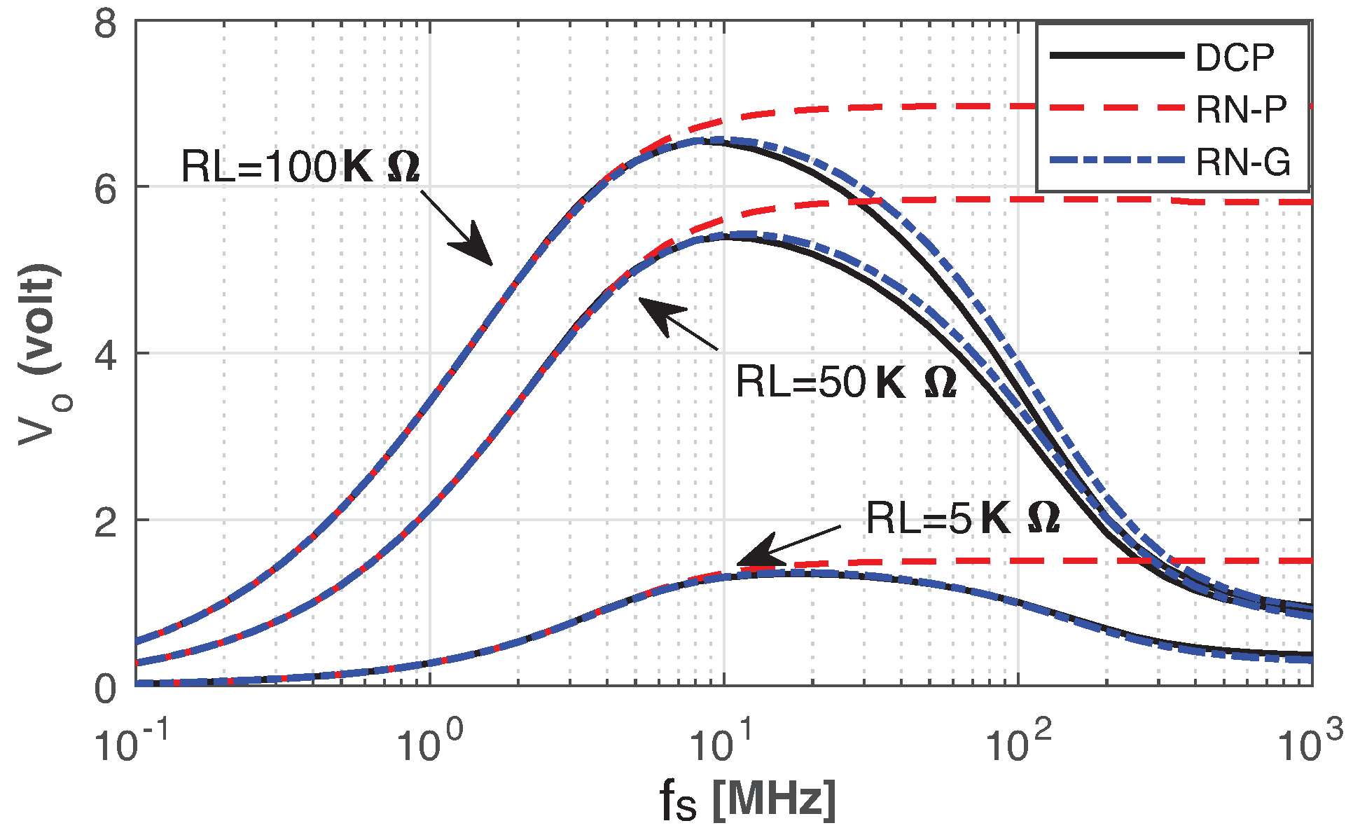
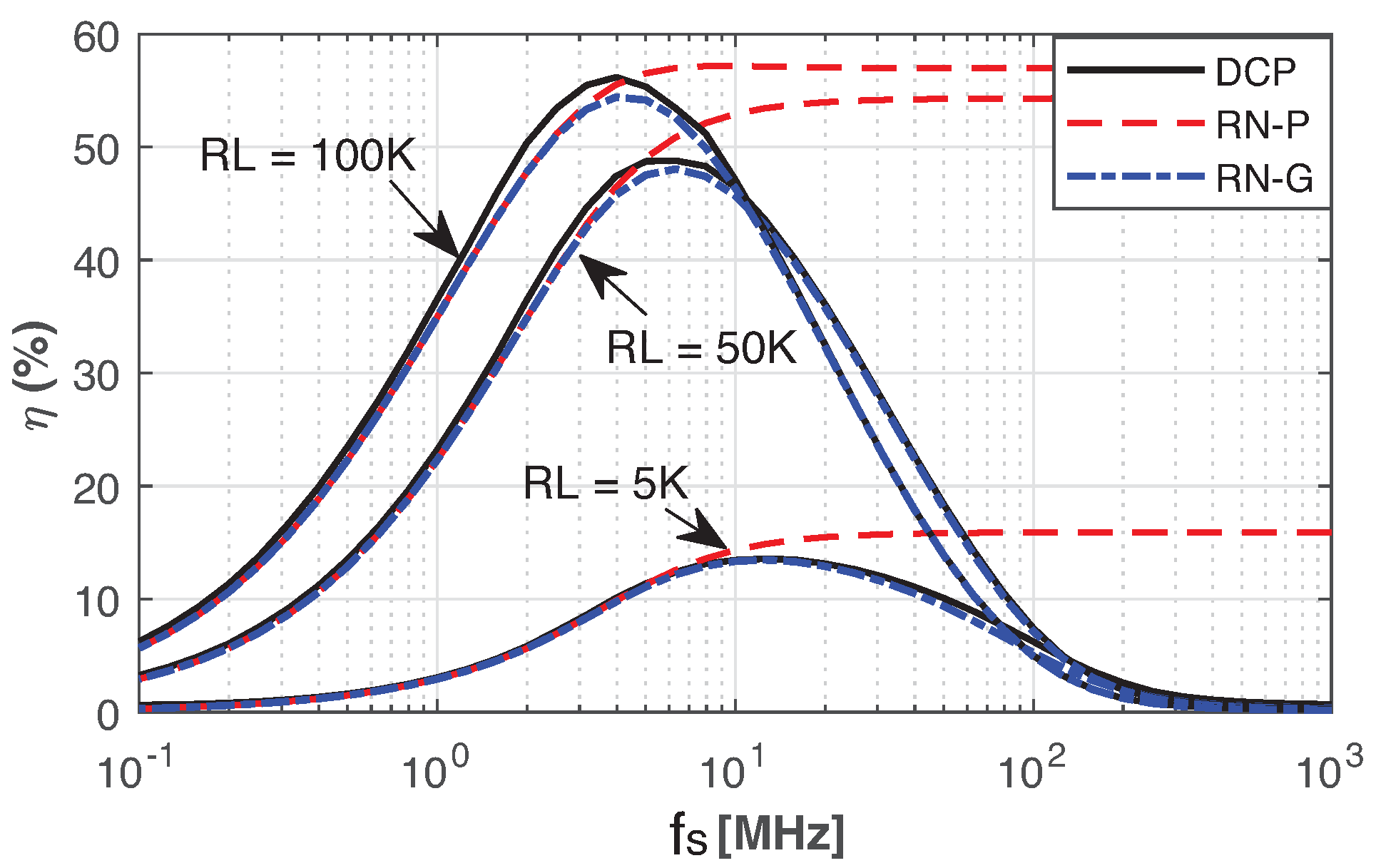
3. Simulation Results

This section provides simulation results using SPICE in Cadence tool to validate the RN model against an actual switching DCP. Three circuits are designed: (i) an 8-stage switching DCP, as in Figure 1; (ii) an 8-stage cascaded RN-P model, as in Figure 11; (iii) an 8-stage RN-G-based model, as in Figure 12. The default design parameters of the circuits are summarized in Table 1.
Figure 15 shows the transient simulation of the output voltage for the switching DCP circuit and the RN-G model at different frequencies. Other parameters are set to default, as in Table 1. As depicted in the figure, the proposed model shows excellent transient and steady-state estimations of the output voltage compared to the switching DCP. For example, at 10 MHz, the error is minimum since the switching frequency is in the mid-range, between ( f c 1 = 6.4 MHz) and ( f c 2 = 256 MHz). In contrast, there is a slight difference as we cone closer to ( f c 2 ), where the DCP shows an output voltage of 3.2 V, while the proposed model predicts 3.4 V. At very high frequencies (1 GHz), the charge pump resistor decreases to the minimum, and the output is less than ( V i n ) due to the extreme effects of the parasitics.
Figure 16 demonstrates the average steady-state output voltage of the switching DCP circuit, RN-G model, and RN-P model at loads of 100-k Ω , 50-k Ω , and 5-k Ω , and different switching frequencies. As shown in Figure 16, the RN-G model accurately predicts the DCP behavior over the whole range of f s since it includes the effects of both the R o n and the parasitic capacitances. In particular, Figure 16 shows the output voltage using the RN-P model, which accounts for the impact of R o n and the parasitic capacitances during SSL and part of the FSL, until f c 1 . The RN-P model accurately predicts the output voltage until f c 1 only, since the RN-P model does not account for the second pole at f c 2 , and the output resistances, R 12 , in Figure 9 stay at τ / c = 6 R o n after f c 1 .
Figure 17 shows the simulation of the power efficiency at loads of 100-k Ω , 50-k Ω and 5-k Ω for the switching DCP, RN-P model, and RN-G model. As indicated in the figure, the proposed RN-G model predicts the efficiency accurately over the entire range of frequencies, with a 2 % error at the maximum efficiency. Moreover, the RN-P model predicts the efficiency accurately until f c 1 . Note that, in practical applications, DCP usually operates at a frequency much less than f c 2 since the VCR of the DCP degrades substantially and has high losses when f s > f c 2 . Therefore, the RN-P model could be used to predict the behavior of the DCP for most applications due to the simple design equations compared to the RN-G model. Finally, both the RN-G and RN-P models provide a fast way to estimate the behavior of DCP approximately 170× faster than the switching DCP circuit when both models and the DCP run on the same CAD tool.
The results shown in Figure 16 and Figure 17 indicate that the proposed RN-G model accurately predicts the output voltage and power efficiency of the DCP over the entire frequency range. Unlike the reported models, the RN-G model accurately predicts the drop of the output voltage in Figure 16, as the frequency increases due to the losses caused by the parasitic capacitances, reflected by the increase in R c h , as was shown in Figure 13. In particular, the proposed model predicts that the output voltage at 1 GHz becomes equal or less than the input at which the DCP is not operating properly. In contrast, the transformer model inaccurately predicts that the VCR of the DCP remains (N + 1) over the entire frequency range, as was explained in Figure 2a. The RC model describes the DCP circuit for low-frequency ranges, and thus does not capture the losses at higher frequencies.

4. Conclusions

We presented a new and simple RN model that accurately describes the electrical characteristics of the DCP. The proposed RN model inherits power conversion properties, as in the transformer model, and exhibits an accurate behavior in the transient and steady-state response, as in the RC model. Unlike the reported models, the RN model describes the behavior of a single-stage DCP, and can be extended to N-stage DCP. The RN model provides a comprehensive insight on various design parameters of the DCP, such as the input/output current, output voltage, load characteristics, power losses, and power efficiency. The RN model provides designers with a simple and effective model to design DCP in a fast and efficient manner for a broad spectrum of applications.

Author Contributions

Conceptualization; methodology; validation; formal analysis; writing—original draft preparation; writing—review and editing, A.S.A. and M.A. All authors have read and agreed to the published version of the manuscript.

Funding

This research received no external funding.

Institutional Review Board Statement

Not applicable.

Informed Consent Statement

Not applicable.

Data Availability Statement

Not applicable.

Conflicts of Interest

The authors declare no conflict of interest.

Abbreviations

The following abbreviations are used in this manuscript:
V i n Input voltage
V Φ Clock high-voltage level
V o Output voltage
V C R Voltage conversion ratio
R p m p Charge pump output resistance
R o n Switches ON-resistance
R o u t Equivalent output resistance
R i j Modeled resistance between i and j terminals
CCharge pump fly capacitor
C p m p Charge pump output capacitance
C L Charge pump load capacitance
C p 1 , C p 2 Top- and bottom-plate capacitance
REquivalent switching resistance
I n ¯ ( t = t 0 ) Average value of I n from ( t 0 ) to ( t o + T )
f c Corner frequency
f s Switching frequency ( = T 1 )
a 1 , a 2 Top and bottom parasitic ratios
τ c , τ d Charging and discharging time constants

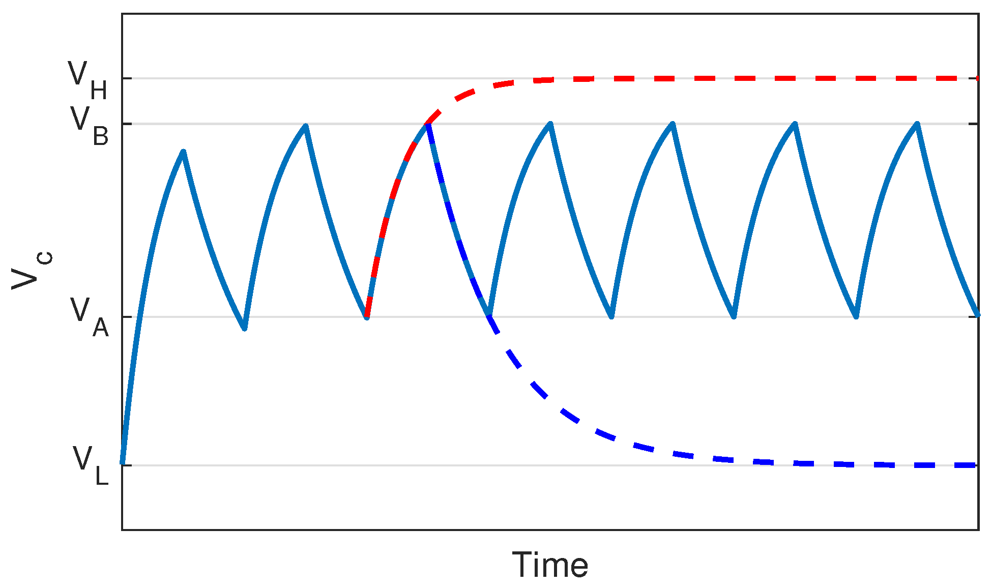
Appendix A. Square Wave Steady-State Response of Single-Pole LTI System

Let us consider a square wave signal, x ( t ) , with an amplitude of ( 1 , + 1 ) , a period (T), and a 50% duty cycle. The signal is an input to a single-pole, linear time-invariant (LTI) system, H ( s ) , where:
H ( s ) = 1 1 + τ s .
The DC gain of H ( s ) is a unity, and x ( t ) has a zero average value; thus, the response of H ( s ) is zero average. If τ < 0 , then H ( s ) is stable, which entails bounded input, resulting in a bounded output.
The output has two phases: rising phase ( Φ 1 ), and falling phase ( Φ 2 ), where in both phases, the curve equation is exponential with the same time constant ( τ = 2 R o n C ). Assuming the output response is confined between (A, B), the output response is:
y = y f + ( y i y f ) e t / τ .
During the first phase, Φ 1 :
y 1 = 1 + ( A 1 ) e t 1 / τ ,
where t 1 is the time relative to the first phase. Thus:
y 1 ( t 1 = 0.5 T ) = B = 1 + ( A 1 ) e T / 2 τ .
During the second phase, Φ 2 :
y 2 = 1 + ( B + 1 ) e t 2 / τ .
Thus:
y 2 ( t 2 = 0.5 T ) = A = 1 + ( B + 1 ) e T / 2 τ .
Solving Equations (A1) and (A2), we obtain:
B = A = tanh T 4 τ .
Therefore, in steady-state, the output is confined between ± tanh T 4 τ . If x ( t ) is a non-zero average, then we can apply the principle of superposition. For instance, if the amplitude of x ( t ) is between ( x m , x M ), with period (T), and 50% duty cycle, then the steady-state output will be shifted by:
y D C = X ¯ × H ( s ) | s = 0 = x m + x M 2 ,
and the steady-state output ripple range is:
x m + x M 2 ± x M x m 2 tanh T 4 τ .
For example, for x ( t ) amplitude of (1, 3), T = 1 s, a 50% duty cycle is introduced to LTI system with transfer function:
H ( s ) = 5 2 s + 1 .
Thus, the steady-state output ripple range is:
1 + 3 2 × 5 1 ± 3 1 2 × 5 × tanh 1 4 ( 2 ) = 10 ± 0.6218 = { 9.3782 , 10.6218 } .
The previous calculation is verified using MATLAB simulation, as shown in Figure A1.
Figure A1. MATLAB Simulation showing the transient and steady-state response of H ( s ) for an input square wave, x ( t ) .
Energies 15 01899 g0a1
In the previous results, each phase in the input is associated with a distinct response at the output:
y 1 = 1 + 2 e t 1 / τ 1 + e t / 2 τ = tanh t 1 4 τ ,
y 2 = + 1 2 e t 2 / τ 1 + e t / 2 τ = tanh t 2 4 τ .
Moreover, it can be proved that:
Y 1 ( τ ) = 0 T / 2 y 1 d t = 2 τ tanh T 4 τ T 2 ,
and:
Y 2 ( τ ) = 0 T / 2 y 2 d t = T 2 2 τ tanh T 4 τ .
The last two equations will help us analyze the circuit in Appendix C.

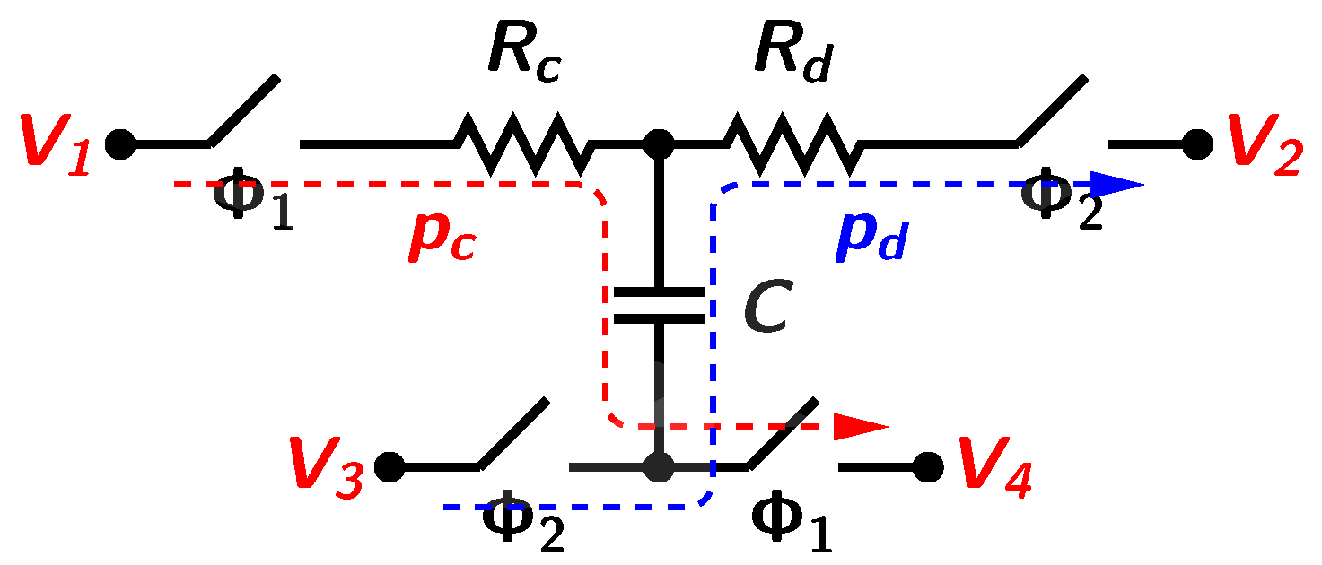
Appendix B. Analysis of Single-Stage CP with Non-Symmetric Charging and Discharging Schemes

Let us consider the simple RC circuit in Figure A2, which has two distinct time constants during the charging and discharging phases: τ c = R c C and τ d = R d C , respectively. All resistances in the charging and discharging paths are lumped into a single resistance, as shown in the figure. Therefore, the voltage across the capacitor, C, at steady-state is shown in Figure A3. During ( Φ 1 ), the voltage across the capacitor, v c , is:
v c ( t 1 ) = V H + ( V H V A ) e t 1 / τ 1 ,
and during ( Φ 2 ):
v c ( t 2 ) = V L + ( V L V B ) e t 2 / τ 2 ,
where V H = V 1 V 4 and V L = V 2 V 3 , at the steady state, v c ( t 1 = 0 ) = v c ( t 2 = T / 2 ) = V A and v c ( t 2 = 0 ) = v c ( t 1 = T / 2 ) = V B , and by solving the two equations, we have:
V B V A V H V L = 1 ( e T / 2 τ c + e T / 2 τ d ) + e T / 2 τ c e T / 2 τ d 1 e T / 2 τ c e T / 2 τ d .
Similar to the same analysis in Section 2 and Section 3, the resistance R:
R = 1 e T / 2 τ c e T / 2 τ d 1 ( e T / 2 τ c + e T / 2 τ d ) + e T / 2 τ c e T / 2 τ d × T C .
Figure A2. Analysis of single-stage DCP with non-symmetric charging and discharging schemes.
Energies 15 01899 g0a2
Figure A3. V c versus time for the circuit in Figure A2.
Energies 15 01899 g0a3

Appendix C. Analysis of Ron and Cp Effects for the RN-G Model

To analyze the circuit in Figure 8, which is equivalent to the circuit shown in Figure A4, we evaluate the linear relationship between V m , V n , and the input square signals V x , V y . By applying Kirchhoff’s voltage law, we obtain:
1 + ( 1 + a 1 ) R o n C s R o n C s R o n C s 1 + ( 1 + a 2 ) R o n C s V m V n = V x V y .
Thus, the characteristic equation:
Δ = ( 1 + ( 1 + a 1 ) R o n C s ) ( 1 + ( 1 + a 2 ) R o n C s ) R o n 2 C 2 s 2 = 1 + ( 2 + a 1 + a 2 ) R o n C s + ( a 1 + a 2 + a 1 a 2 ) R o n 2 C 2 s 2 .
Thus:
H m ( s ) = 1 + ( 1 + a 2 ) R o n C s Δ H mx V x + R o n C s Δ H my V y .
This system has two real, negative poles associated with the following time constants:
τ 1 2 + a 1 + a 2 2 R o n C ,
τ 2 a 1 + a 2 2 R o n C .
Using partial fraction:
H mx ( s ) = ( τ 1 ( 1 + a 2 ) R o n C ) ( τ 1 τ 2 ) ( 1 + τ 1 s ) + ( ( 1 + a 2 ) R o n C ) τ 2 ( τ 1 τ 2 ) ( 1 + τ 2 s )
H my ( s ) = 1 τ 1 τ 2 0.5 1 + τ 1 s 0.5 1 + τ 2 s
The node V m has a DC value of:
V m ¯ = V x ¯ × H mx ( s = 0 ) + V y ¯ × H my ( s = 0 ) = V 1 + V 2 2 .
The steady-state ripple of V m can be evaluated by multiplying the half of the clock peak-to-peak value by the standard square wave unity response y 1 , and we obtain the following components:
  • ( τ 1 ( 1 + a 2 ) R o n C ) τ 1 τ 2 × V 2 V 1 2 × y 1 τ 1 ;
  • ( τ 1 ( 1 + a 2 ) R o n C ) τ 1 τ 2 × V 2 V 1 2 × y 1 τ 2 ;
  • 1 τ 1 τ 2 × V 3 V 4 2 × y 1 τ 1 ;
  • 1 τ 1 τ 2 × V 3 V 4 2 × y 1 τ 2 .
Figure A4. R o n , C p effects analysis.
Energies 15 01899 g0a4
During Φ 1 , the average current, I 1 ¯ , in Figure 8 is:
I 1 ¯ = 1 T 0 0.5 T V 1 V m R o n d t .
Thus:
I 1 ¯ = 1 T R o n ( V 1 T 2 ( V 1 + V 2 ) T 4 ( τ 1 ( 1 + a 2 ) R o n C ) τ 1 τ 2 × V 2 V 1 2 × Y 1 τ 1 ( τ 1 ( 1 + a 2 ) R o n C ) τ 1 τ 2 × V 2 V 1 2 × Y 1 τ 2 + 1 τ 1 τ 2 × V 3 V 4 2 × Y 1 τ 1 1 τ 1 τ 2 × V 3 V 4 2 × Y 1 τ 2 ) .
Thus:
G 12 = 1 R 12 = I 1 ¯ V 1 V 2 | V 3 = V 4 = τ 1 ( τ 1 ( 1 + a 2 ) R o n C ) T R o n ( τ 1 τ 2 ) tanh T 4 τ 1 + τ 2 ( ( 1 + a 2 ) R o n C τ 2 ) T R o n ( τ 1 τ 2 ) tanh T 4 τ 2 .
Thus:
G 14 = 1 R 14 = I 1 ¯ V 1 V 2 | V 3 = V 4 = 1 R o n ( τ 1 τ 2 ) τ 1 T tanh T 4 τ 1 τ 2 T tanh T 4 τ 2
G 13 = 1 R 13 = G 14 = 1 R o n ( τ 1 τ 2 ) τ 1 T tanh T 4 τ 1 τ 2 T tanh T 4 τ 2 .
Performing the same analysis on V y :
G 34 = 1 R 34 = τ 1 ( τ 1 ( 1 + a 1 ) R o n C ) T R o n ( τ 1 τ 2 ) tanh T 4 τ 1 + τ 2 ( ( 1 + a 1 ) R o n C τ 2 ) T R o n ( τ 1 τ 2 ) tanh T 4 τ 2 .
Therefore, the resistance values of the RN-G model are calculated and can be used to estimate the behavior of the DCP circuit.

References

  1. Wong, O.; Wong, H.; Tam, W.; Kok, C. A comparative study of charge pumping circuits for flash memory applications. Microelectron. Reliab. 2012, 52, 670–687. [Google Scholar] [CrossRef]
  2. Mahmoud, A.; Alhawari, M.; Mohammad, B.; Saleh, H.; Ismail, M. A gain-controlled, low-leakage Dickson charge pump for energy-harvesting applications. IEEE Trans. Very Large Scale Integr. Syst. 2019, 27, 1114–1123. [Google Scholar] [CrossRef]
  3. Ballo, A.; Grasso, A.D.; Palumbo, G. A Review of Charge Pump Topologies for the Power Management of IoT Nodes. Electronics 2019, 8, 480. [Google Scholar] [CrossRef] [Green Version]
  4. Chen, P.; Cheng, H.; Lo, C. A Single-Inductor Triple-Source Quad-Mode Energy-Harvesting Interface With Automatic Source Selection and Reversely Polarized Energy Recycling. IEEE J. Solid State Circuits 2019, 54, 2671–2679. [Google Scholar] [CrossRef]
  5. Alhawari, M.; Mohammad, B.; Saleh, H.; Ismail, M. An Efficient Polarity Detection Technique for Thermoelectric Harvester in L-based Converters. IEEE Trans. Circuits Syst. Regul. Pap. 2017, 64, 705–716. [Google Scholar] [CrossRef]
  6. Ma, D.; Bondade, R. Fundamental Charge Pump Topologies and Design Principles. In Reconfigurable Switched-Capacitor Power Converters; Springer: New York, NY, USA, 2013; ISBN 978-1-4614-4187-8. [Google Scholar]
  7. Seeman, M.; Sanders, S. Analysis and Optimization of Switched-Capacitor DC-DC Converters. IEEE Trans. Power Electron. 2008, 23, 841–851. [Google Scholar] [CrossRef]
  8. Ferro, E.; Brea, V.; Lopez, P.; Cabello, D. Dynamic Model of Switched-Capacitor DCDC Converters in the Slow-Switching Limit Including Charge Reusing. IEEE Trans. Power Electron. 2017, 32, 5293–5311. [Google Scholar] [CrossRef]
  9. Pasternak, S.; Kiani, M.; Rentmeister, J.; Stauth, J. Modeling and Performance Limits of Switched-Capacitor DC-DC Converters Capable of Resonant Operation With a Single Inductor. IEEE J. Emerg. Sel. Top. Power Electron. 2017, 5, 1746–1760. [Google Scholar] [CrossRef]
  10. Tanzawa, T. Dickson charge pump circuit design with parasitic resistance in power lines. In Proceeding of the IEEE International Symposium on Circuits and Systems, Taipei, Taiwan, 24–27 May 2009; pp. 1763–1766. [Google Scholar]
  11. Erickson, R.; Maksimovic, D. Fundamentals of Power Electronics; Springer International Publishing: Cham, Switzerland, 2020. [Google Scholar]
  12. Hella, M.M.; Mercier, P. Power Management Integrated Circuits; CRC Press: Cham, Switzerland, 2016. [Google Scholar]
  13. Gregori, S.; Rotunno, R.E. z-Domain analysis of Dickson charge pumps. In Proceeding of the IEEE International Conference on Electronics, Circuits and Systems (ICECS), Monte Carlo, Monaco, 11–14 December 2016; pp. 185–188. [Google Scholar]
  14. Ballo, A.; Bottaro, M.; Grasso, A.D.; Palumbo, G. A General Behavioral Model of Charge Pump DC-DC converters. In Proceeding of the International Conference on Electrical, Communication, and Computer Engineering (ICECCE), Istanbul, Turkey, 12–13 June 2020; pp. 1–4. [Google Scholar]
  15. Ballo, A.; Grasso, A.D.; Palumbo, G.; Tanzawa, T. Charge Pumps for Ultra-Low-Power Applications: Analysis, Design, and New Solutions. IEEE Trans. Circuits Syst. II Express Briefs 2021, 68, 2895–2901. [Google Scholar] [CrossRef]
  16. Ballo, A.; Bottaro, M.; Grasso, A.D.; Palumbo, G. Regulated Charge Pumps: A Comparative Study by Means of Verilog-AMS. Electronics 2020, 9, 998. [Google Scholar] [CrossRef]
  17. Tanzawa, T. On-chip High-Voltage Generator Design; Springer International Publishing: Cham, Switzerland, 2016. [Google Scholar]
  18. Tanzawa, T. A Switch-Resistance-Aware Dickson Charge Pump Model for Optimizing Clock Frequency. IEEE Trans. Circuits Syst. II Express Briefs 2011, 58, 336–340. [Google Scholar] [CrossRef]
  19. Tanzawa, T. A Behavior Model of a Dickson Charge Pump Circuit for Designing a Multiple Charge Pump System Distributed in LSIs. IEEE Trans. Circuits Syst. Express Briefs 2010, 57, 527–530. [Google Scholar] [CrossRef]
  20. Tan, Y.; Ishikuro, H. A Discrete-Time Model for Frequency Modulated Charge Pumps with Synchronized Controller. In Proceeding of the IEEE 63rd International Midwest Symposium on Circuits and Systems (MWSCAS), Springfield, MA, USA, 9–12 August 2020; pp. 929–932. [Google Scholar]
  21. Ma, D.; Bondade, R. Switched-Capacitor Power Converter Design and Modeling in z-Domain. In Reconfigurable Switched-Capacitor Power Converters; Springer: New York, NY, USA, 2013; ISBN 978-1-4614-4187-8. [Google Scholar]
  22. Cabrini, A.; Gobbi, L.; Torelli, G. Theoretical and Experimental Analysis of Dickson Charge Pump Output Resistance. In Proceedings of the 2006 IEEE International Symposium on Circuits and Systems, Island of Kos, Greece, 21–24 May 2006; p. 4. [Google Scholar] [CrossRef]
  23. Tanzawa, T. A Behavior Model of an On-Chip High Voltage Generator for Fast, System-Level Simulation. IEEE Trans. Very Large Scale Integr. Syst. 2012, 20, 2351–2355. [Google Scholar] [CrossRef]
  24. Karagozler, M.E.; Goldstein, S.C.; Ricketts, D.S. Analysis and Modeling of Capacitive Power Transfer in Microsystems. IEEE Trans. Circuits Syst. Regul. Pap. 2012, 59, 1557–1566. [Google Scholar] [CrossRef] [Green Version]
  25. Sommariva, A. Solving the two capacitor paradox through a new asymptotic approach. IEEE Proc. Circuits Devices Syst. 2003, 150, 227. [Google Scholar] [CrossRef]
  26. Tanzawa, T. On the Output Impedance and an Output Current–Power Efficiency Relationship of Dickson Charge Pump Circuits. IEEE Trans. Circuits Syst. II 2018, 65, 1664–1667. [Google Scholar] [CrossRef]
  27. Dickson, J.F. On-chip high-voltage generation in MNOS integrated circuits using an improved voltage multiplier technique. IEEE J. Solid State Circuits 1976, 11, 374–378. [Google Scholar] [CrossRef]
  28. Talkhooncheh, A.; Yu, Y.; Agarwal, A.; Kuo, W.; Chen, K.; Wang, M.; Hoskuldsdottir, G.; Gao, W.; Emami, A. A Biofuel-Cell-Based Energy Harvester With 86% Peak Efficiency and 0.25-V Minimum Input Voltage Using Source-Adaptive MPPT. IEEE J. Solid State Circuits 2021, 56, 715–728. [Google Scholar] [CrossRef]
  29. Aloqlah, A.S.; Alhawari, M. Demystifying Maximum Power Transfer Methodologies for Charge Pumps: An Analytical Approach. Proceeding of the IEEE International Midwest Symposium on Circuits and Systems (MWSCAS), Lansing, MI, USA, 9–11 August 2021; pp. 978–981. [Google Scholar]
  30. Liu, X.; Ravichandran, K.; Sanchez-Sinencio, E. A Switched Capacitor Energy Harvester Based on a Single-Cycle Criterion for MPPT to Eliminate Storage Capacitor. IEEE Trans. Circuits Syst. Regul. Pap. 2018, 65, 793–803. [Google Scholar] [CrossRef]
  31. Liu, X.; Huang, L.; Ravichandran, K.; Sanchez-Sinencio, E. A Highly Efficient Reconfigurable Charge Pump Energy Harvester With Wide Harvesting Range and Two-Dimensional MPPT for Internet of Things. IEEE J. Solid State Circuits 2016, 51, 1302–1312. [Google Scholar] [CrossRef]
Figure 1. Circuit diagram of N-stage DCP.
Energies 15 01899 g001
Figure 2. Various models of DCP: (a) Transformer model [15,16]; (b) RC model [17].
Energies 15 01899 g002
Figure 3. Circuit diagram of a single-stage DCP connected to a load.
Energies 15 01899 g003
Figure 4. Single-stage DCP modeling.
Energies 15 01899 g004
Figure 5. The proposed RN model for single-stage DCP during SSL.
Energies 15 01899 g005
Figure 6. The equivalent resistance R with frequency for single-stage DCP when accounting for the switch ON-resistance.
Energies 15 01899 g006
Figure 7. Equivalent resistance approximation from Equations (16) and (13).
Energies 15 01899 g007
Figure 8. Single-stage DCP, including parasitic capacitors.
Energies 15 01899 g008
Figure 9. The RN-P model includes the effect of C p 1 and C p 2 .
Energies 15 01899 g009
Figure 10. Analysis of the RN-P model, including C p 1 and C p 2 .
Energies 15 01899 g010
Figure 11. RN-P model representation of N-stage DCP using cascaded resistive networks.
Energies 15 01899 g011
Figure 12. The RN-G model.
Energies 15 01899 g012
Figure 13. RN-G model characteristics summary for the case when τ a v g = 2 R o n C , showing the behavior of various resistors, including R as a reference.
Energies 15 01899 g013
Figure 14. Charging and discharging paths between two consequent intermediate stages in DCP.
Energies 15 01899 g014
Figure 15. Time-domain SPICE simulation of the output voltage at different frequencies for the switching DCP and the RN-G.
Energies 15 01899 g015
Figure 16. SPICE simulation of the output voltage at different switching frequencies and loads for the switching DCP circuit, RN-P model, and RN-G model.
Energies 15 01899 g016
Figure 17. SPICE simulation of the power efficiency vs. f s at different loads for the switching DCP circuit, RN-P, and RN-G models.
Energies 15 01899 g017
Table 1. Simulation Parameters.
ParameterValue
N8
f s 10 MHz
C50 pF
C L 500 pF
a 1 5%
a 2 5%
R o n 500 Ω
R L 50 k Ω
V i n 1 volt
D u t y C y c l e 50%
Publisher’s Note: MDPI stays neutral with regard to jurisdictional claims in published maps and institutional affiliations.

