Article

Design, Control and Testing of a Modular Multilevel Converter with a Single Cell per Arm in Grid-Forming and Grid-Following Operations for Scaled-Down Experimental Platforms

by
Jaume Girona-Badia
1,*,
Oriol Gomis-Bellmunt
1,
Tomàs Lledó-Ponsati
1,
Macià Capó-Lliteras
1,
Carlos Collados-Rodriguez
1,
Nicolaos Antonio Cutululis
2,
Oscar Saborío-Romano
2,
Daniel Montesinos-Miracle
1,
Marc Pagès
3,
Daniel Heredero-Peris
1 and
Eduardo Prieto-Araujo
1
1
CITCEA-UPC, Department of Electrical Engineering, Universitat Politècnica de Catalunya, Av. Diagonal 647, 08028 Barcelona, Spain
2
Department of Wind Energy, Technical University of Denmark, Frederiksborgvej 399, 115, S29, 4000 Roskilde, Denmark
3
TeknoCEA, C/Roca Umbert, nº 16, Baixos G., L’Hospitalet de Llobregat, 08907 Barcelona, Spain
*
Author to whom correspondence should be addressed.
Energies 2022, 15(5), 1819; https://doi.org/10.3390/en15051819
Submission received: 24 November 2021 / Revised: 22 February 2022 / Accepted: 24 February 2022 / Published: 1 March 2022
(This article belongs to the Special Issue Design, Modeling and Control of Power Converters)

Abstract

:
Modular multilevel converters (MMC) can be used in several applications, especially (but not only) in high-voltage direct current (HVDC) and STATCOM. In order to develop experimental scaled-down test benches for lab validation, several projects have developed MMCs with a limited number of cells, but they need to use pulse width modulation (PWM) techniques to achieve acceptable power quality (because nearest level modulation (NLM), common in HVDC applications with hundreds of levels, cannot achieve sufficient power quality unless the number of cells is high enough). The present paper proposes a new concept which is based on designing arms with a single cell. This allows to have the simplest possible converter that maintains the structure of an MMC. While all the inner controllers of large-scale HVDC MMCs are included, the only remarkable difference is that PWM is used and NLM cannot be implemented. As this is also a limitation for other low voltage MMC, the proposed concept is suggested for scaled-down low voltage applications. The paper includes the design and construction of the converter, the definition and implementation of the converter controllers, and the converter testing, with detailed dynamic simulations and an experimental setup.

1. Introduction

Modern power systems are increasingly populated by high-voltage direct current (HVDC) and flexible alternating-current transmission systems (FACTS) [1]. HVDC technology is mainly used for bulk power transmission over long distances (approximately longer than 600–800 km for overhead lines or 100 km for underground or submarine cables [2]), interconnection of non-synchronous power systems (with or without the same nominal frequency) and connection of remote renewable power plants (such as remote offshore wind power plants) [2]. FACTS equipment is used in several applications to increase the AC power system flexibility providing an enhanced control of its AC bus voltages and lines currents and powers. Both for FACTS and HVDC applications, voltage source converter (VSC) technology, based on fast-switching semiconductors, such as IGBT, is preferred over line commutated converter (LCC) technology based on thyristors, because of the capacity of forming a grid (or black-starting it), requiring less (or none) filtering and reactive power compensation equipment and allowing independent active and reactive power control.
Among the different possible VSC technologies, modular multilevel converters (MMC) are achieving high efficiencies (comparable to LCC), while presenting all VSC functionalities in a modular structure. Therefore, MMC is the selected technology for most recent VSC-based HVDC projects worldwide. As far as FACTS are concerned, MMCs are being used in modern STATCOM equipment (including STATCOM applications with storage).
MMC modeling and control has been extensively addressed in several works [3,4], based on an energy-based control approach. Energy control approach allows to have independent control of AC and DC power and therefore an additional degree of freedom can be used storing (limited) energy in the cells of the MMC. Several projects have developed scaled experimental platforms [3,5] to experimentally validate the proposed concepts.
The present work proposes an MMC concept using a single cell per arm. This allows to maintain the MMC structure (and associated inner and energy controllers) with the minimum number of semiconductors and cells, enabling conduction of several studies without requiring more complex systems. The only controllers that cannot be tested are related to the sorting algorithms associated to nearest level modulation (NLM) techniques typically applied in high-voltage MMCs, due to the single-level implementation. Regarding this last issue, it is important to remark that other scaled MMCs with low number of cells share this same problem and need as well to implement pulse width modulation (PWM) techniques in some (or all) the cells to operate the converter. Therefore, it can be stated that the one cell per arm concept can be used to perform the same studies as similar converters with higher number of cells per arm, since, in all cases, PWM is required anyway.
To summarize, the proposed converter is a simple and low-cost converter structure that can include all the relevant controllers existing in an MMC.
The rest of the paper is structured as follows. Section 2 introduces the converter concept, the specifications and the converter design. The control is analyzed in Section 3, presenting both the theoretical foundations and the practical implementation for grid-forming and grid-following modes. The experimental and simulation validations is discussed in Section 4, where the converter is tested in different conditions. Section 5 includes the discussion. Finally, the conclusions are summarized in Section 6.

2. MMC with One Cell per Arm

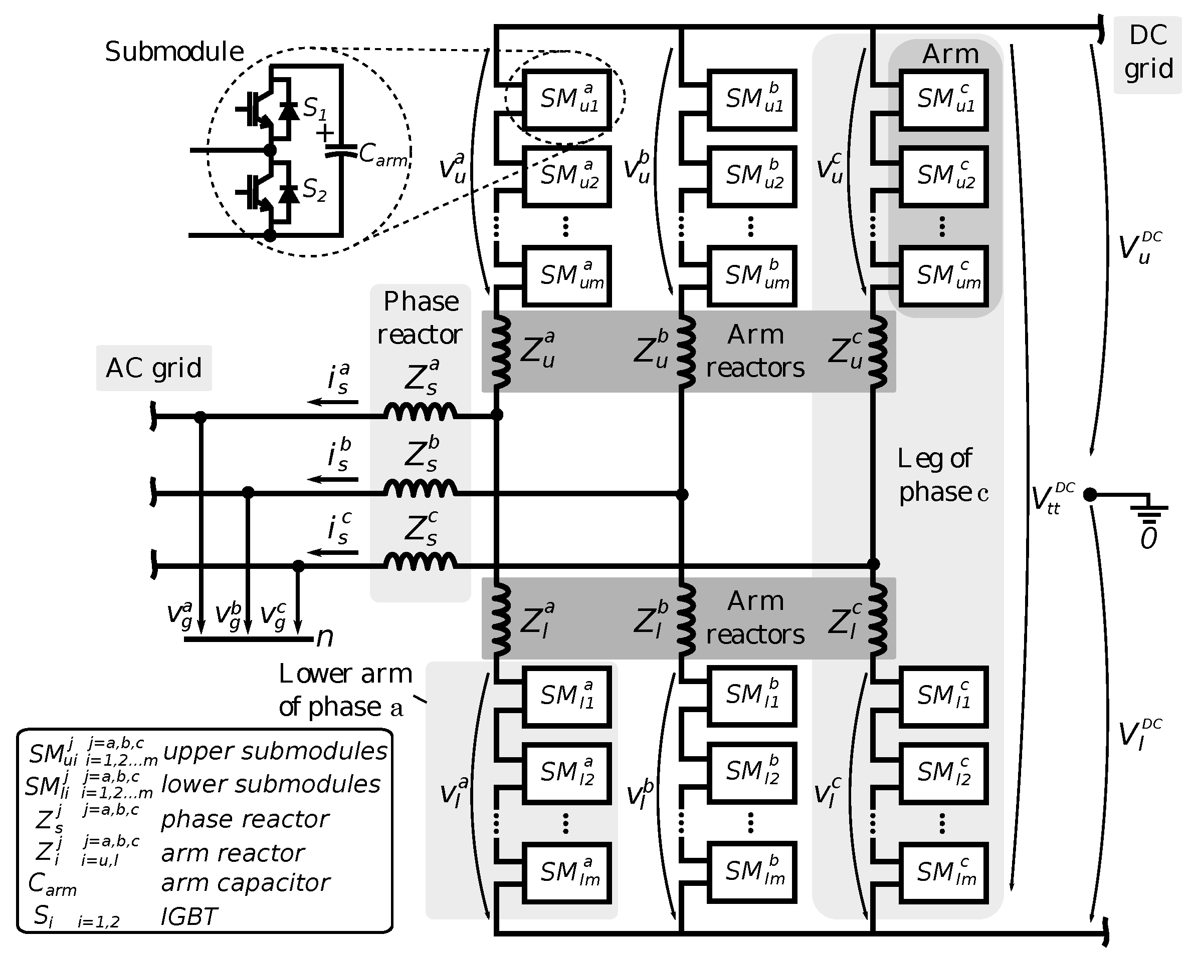
2.1. Converter Concept

Several manufacturers are developing and installing modular multilevel converters (see Figure 1) for several purposes, especially for VSC-HVDC transmission and STATCOM applications. When the number of cells is sufficiently high (which is the case for high-voltage applications, due to the high number of cells required) the preferred modulation technique is nearest level modulation (NLM), which basically modulates voltages in a “staircase” approach, dramatically reducing the switching frequency and the associated losses. For research and testing purposes, several research projects have developed scaled MMC experimental platforms at low- or medium-voltage levels, where the number of cells per arm is significantly reduced [3,5,6,7,8,9,10,11,12,13,14,15,16,17,18,19,20]. While some of the converters’ cells can be operated using an NLM technique, in order to obtain acceptable power quality, some of the cells need to be operated with pulse width modulation (PWM). An example of this is shown in Figure 2, where a voltage signal is modulated with converters with 1, 2, 7 and 11 cells per arm. In the left column, only NLM is applied. As this is not sufficient to achieve good power quality in all conditions (including disturbances and faults), PWM in at least one level is implemented as shown in the right column. This limits the feasibility of accurate replication of MMC modulation in scaled low-/medium-voltage setup, as real high-voltage MMCs with hundreds of cells per levels can operate only in NLM. Following this reasoning, the concept proposed in this paper assumes that the modulation cannot be replicated and it proposes to develop a converter with only one cell per arm, operated in PWM. The converter keeps the basic MMC structure and includes the inherent energy storage capacity in the arms capacitors, controlling the arm energies, as it happens in large MMC converters. The converter also includes the superposition of AC and DC currents and voltages in the arms, and the obtained waveforms are equivalent to those of large MMCs. The only significant difference is that NLM is not applied, but, as mentioned above, the same is true for scaled MMCs with several cells per arm, as have been developed in previous studies.
Figure 3 shows an scheme of the proposed converter topology, in its half-bridge and full-bridge cell versions. Each converter arm is composed of a single cell and an arm inductor. A transformer is used to couple the converter to the grid.

2.2. Specifications

The converter can be designed for different possible specifications. In this paper, the specifications oriented for an MMC scaled laboratory setup can be summarized as follows:
  • The MMC converter (one cell per arm) includes inner energy controllers, circulating current and relevant controls;
  • The converter can be used with half or full bridge cells;
  • The converter will be installed in a cabinet including isolation transformers, converter reactors, filters, circuit breakers, measurements and protections;
  • The converter rated power is 10 kVA and has to control independently P and Q in rectifier/inverter mode;
  • The converter needs to be able to operate in grid-forming and grid-following modes;
  • DC voltage shall be in the range from 450 V to 800 V and the supplied AC voltage is of 400 V (3-ph L-L RMS);
  • The converter shall be able to operate at +/−10% of rated AC voltage supply and withstand AC faults.;
  • The converter shall be able to operate at the frequencies between 40 and 60 Hz.

2.3. Converter Design

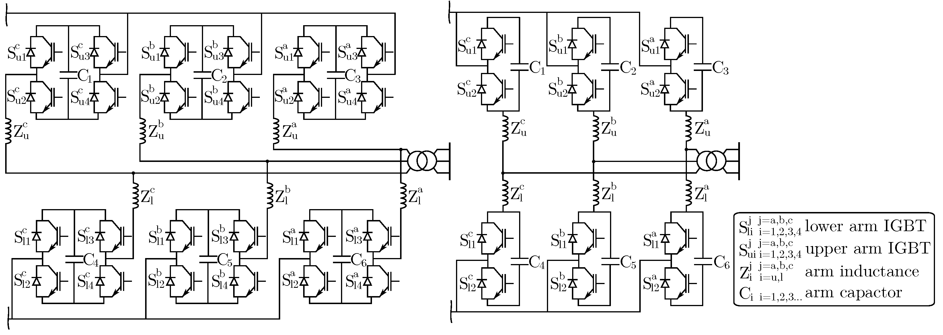
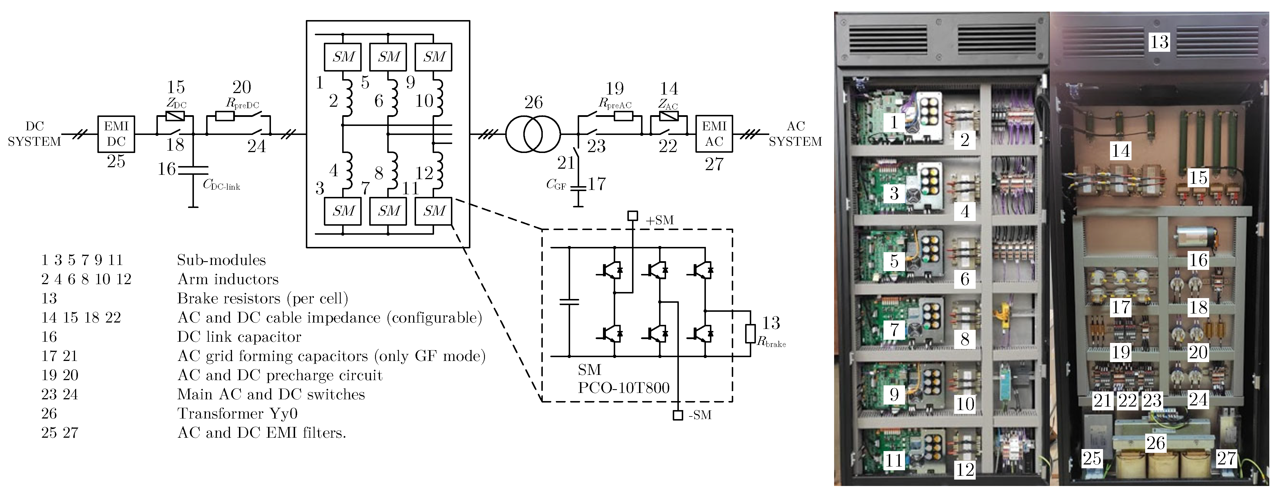
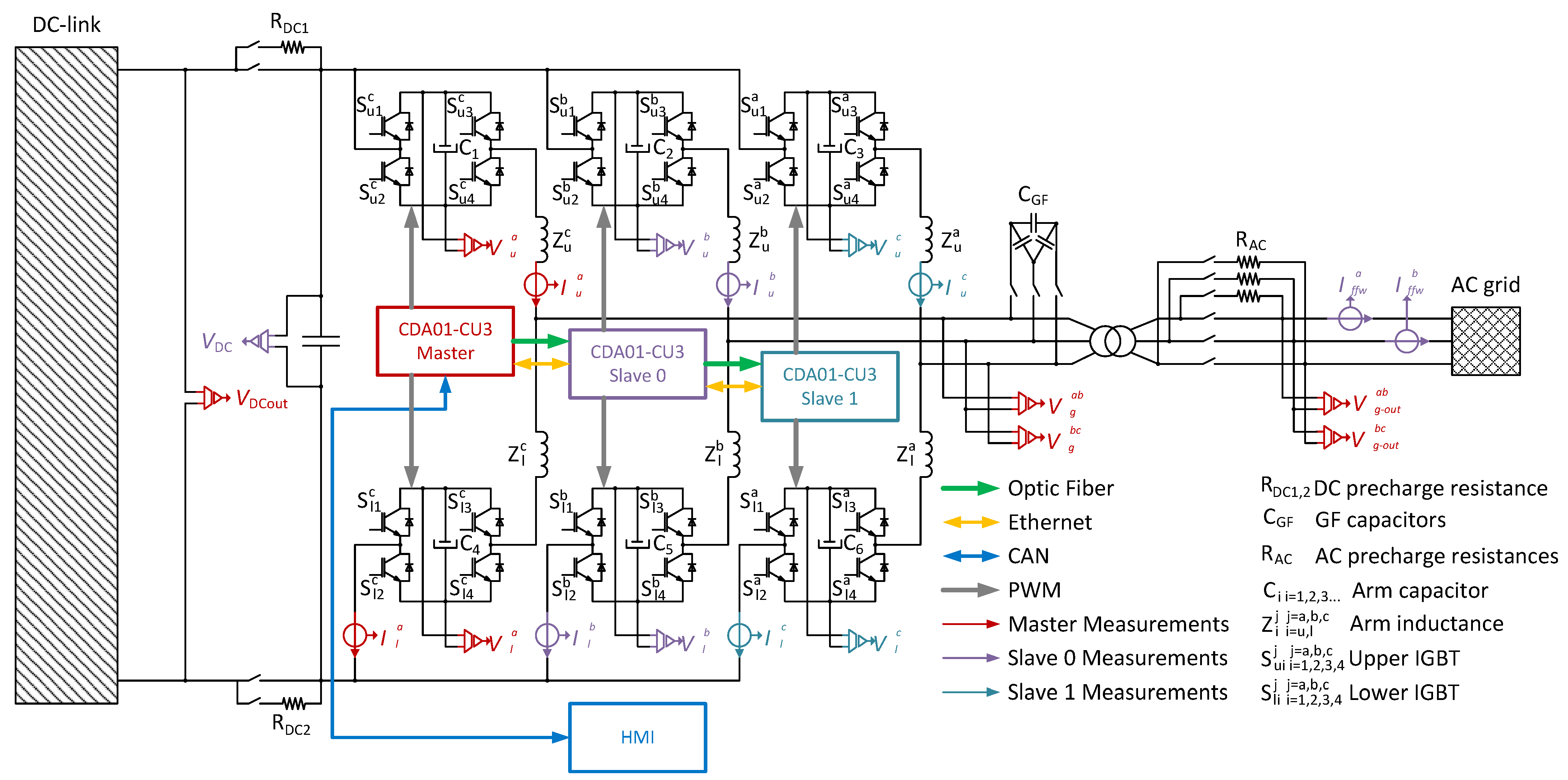
2.3.1. Converter Layout and Power Modules

Figure 4 shows the single-line diagram of the analyzed converter. The different elements are labeled for easy identification of their position in the cabinet. The MMC power converter is based on the three-phase teknoCEA PCO-10T800 inverter module [21] and the CDA01-CU3 teknoCEA control board [22]. Each cell (1, 3, 5, 7, 9 and 11) is implemented with 1 PCO-10T800. One CDA01-CU3 is used to control every two PCO-10T800. The PCO-10T800 is a power electronics platform designed as a three-phase inverter with sufficient adaptability to implement other topologies. Consequently, the equipment includes more current and voltage measurements than necessary for a three-phase inverter. Additionally, it includes several digital outputs to control the necessary switchgear associated. Operating as a three-phase inverter, the PCO-10T800 is rated for 10 kVA, connected to a 400 VRMS grid and DC-link voltage between 650 and 800 V. The power converter is based on Si IGBTs with a maximum switching frequency of 20 kHz, based on a SkiiP 23AC12T4v1 IGBT4 Trench module from Semikron. The CDA01-CU3 control board is a general purpose control board based on a Texas Intruments F28M35 microcontroller. The CDA01-CU3 control board has a direct interface connection with two PCO-10T800.
As shown in Figure 4 the three legs of each PCO-10T800 are used. Two of them are used to create the full-/half-bridge cell and the third one is used to control the power dissipation in the brake resistance, which is distributed per arm. Together with the power converters, the inductances, capacitors and all the necessary AC/DC switchgear are installed in the cabinet. Impedances at both the AC side and the DC side can be added to emulate grid equivalent impedances.

2.3.2. Arm Inductance Sizing and Selection

The arm inductance has been sized to limit the short-circuit current of the converter for AC faults, DC faults and possible direct connection between upper and lower arms that can occur during switching. (This overlap will be minimized by means of the modulation strategy implemented, but the inductance ensures that there is no problem if this happens). Considering the above premises, the inductance of the MMC arm has been selected as 5.1 mH, which corresponds to an equivalent short-circuit reactance of 0.15 pu (association of two parallel arms with reactance of 0.3 pu). A switching frequency of 10 kHz is selected as it is the minimum frequency that ensures the expected ripple according to the designed inductance, so converter losses are minimized. Figure 5 shows an example of the arm currents simulated with a switched model, where it can be noticed that the ripple is limited to 6.25%. Arm inductances have been selected bearing in mind only their DC and grid frequency current components (considering specifications between 40 and 60 Hz). The core is made of laminated steel and the winding of solid copper. The inductors are rated for a DC current of 8.5 A and an AC component of 12.55 ARMS.

2.3.3. Cell Capacitor Sizing and Selection

The cell capacitance has to be chosen considering the trade off between voltage ripple in the capacitor cells (increases with smaller capacitances) and converter volume and cost (increases with higher capacitances). The cell capacitance has been designed analyzing the voltage ripple variation for different DC voltages and capacitance values. The smallest capacitance, C = 1.02 mF, which secures a limited voltage ripple, has been chosen. The capacitance obtained has been further validated using a typical ratio, ρ e p = E / P n o m = C V 2 / 2 P n o m , of total stored energy per nominal power which should be larger than 30 kJ/MW [1]. The total stored energy is 61.96 kJ/MW at 450 V (min voltage—worst case).
Simulations and experiments have validated that this capacitor value ensures a correct maximum voltage cell ripple of 10 % in the worst case possible (in the case of low DC voltage, see Figure 5).
The cell capacitor is formed by the series connection of two blocks of three parallel, connected 680 µF electrolytic capacitors with a nominal voltage of 450 V. The total capacitance is 1020 µF with a 900 V of nominal voltage. Two 47 k Ω resistors are used to balance capacitor voltages.

2.3.4. Converter Control Architecture

Figure 6 shows a schematic view of the MMC converter together with the control: human–machine interface (HMI) and three control boards. The control boards are highlighted in different colors. The measurements of the MMC are depicted in the same color as the control board performing the measurement. The MMC control algorithms are programmed in the Master CDA01-CU3. The two slave control boards send the current and voltage measurements to the master control board, and receive from the master the modulation index for the upper and lower arm. All this information is shared using a precision time protocol (PTP) Ethernet interface. The PTP Ethernet interface provides sufficient transmission speed for the measurements sampled at switching frequency and modulation index. The three control boards are synchronized between them using optic fiber. The system is controlled with an external HMI, connected with a CAN interface.

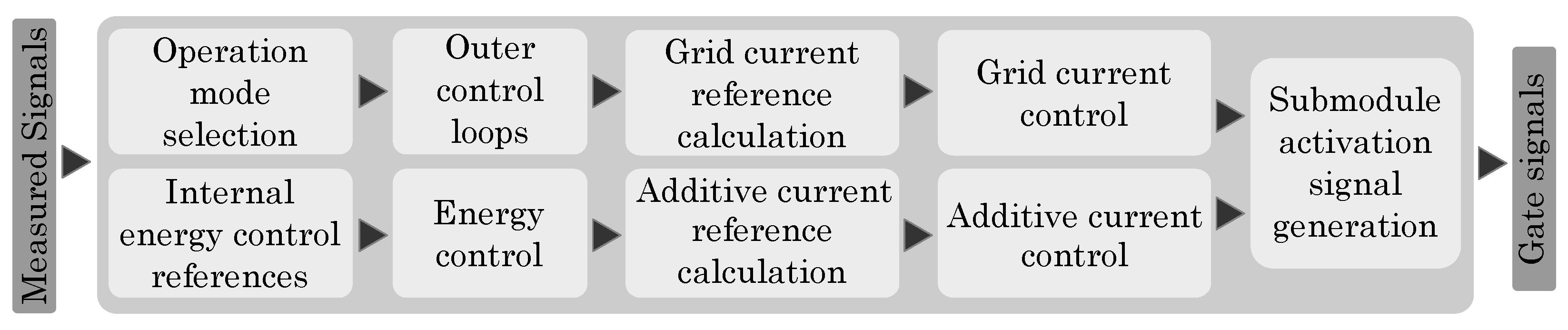
3. Control Structure

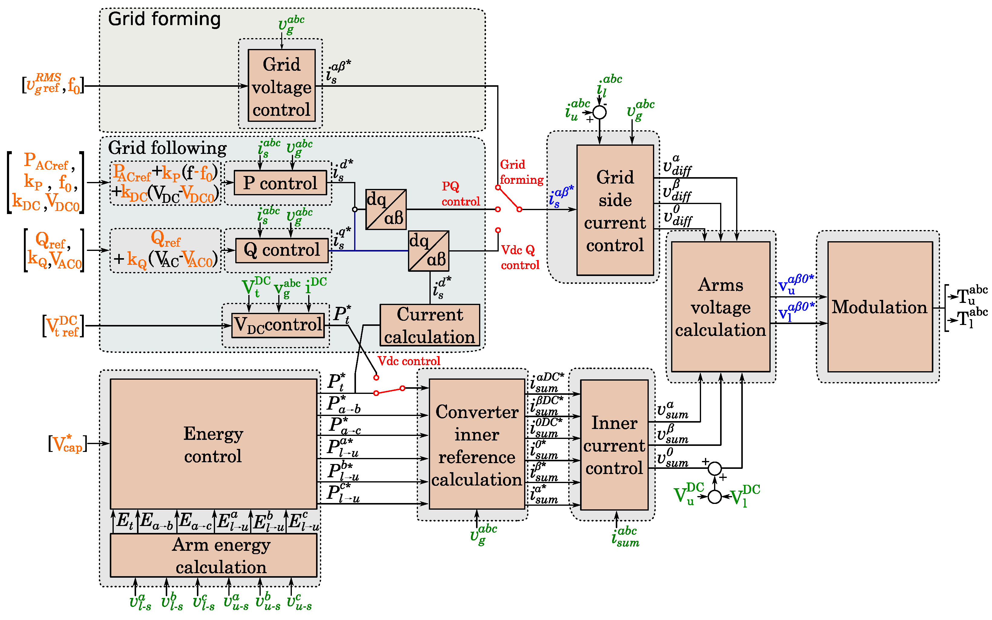
3.1. Overall Control Structure

The MMC can operate in two control modes: grid forming and grid following. Their description is detailed below:
  • Grid-following mode: This converter control strategy relies on an existing AC network to implement its controllers. They require a network orientation structure, typically called phase locked loop (PLL), which measures the AC grid voltage, extracting the voltage and angle (and frequency) of the network. The control options considered are the following:
    -
    P Q control: It regulates the active and reactive power exchanged by the converter. This control needs a regulated DC link voltage to operate;
    -
    The V d c -Q control: It regulates the DC link voltage and the reactive power exchanged;
    -
    Supporting controllers: Additional loops to support network AC frequency, AC voltage or a DC distributed voltage droop control could also be included, as supplementary controllers.
  • Grid-forming mode: It does not rely on an existing network. The control forms a grid and imposes voltage and angle at the point of connection to the AC network.

3.2. Operating Principle and Modeling

Once the upper level control strategies have been defined, the basic operating principle of the MMC is explained. The suggested MMC structure has a single cell per arm, which can be controlled to behave as a controllable voltage source (fed from a capacitor energy storage device). Then, these synthesized arm voltage sources can be used to control the AC and DC current components flowing through the converter. These currents references will be defined both to implement the selected converter control mode and to maintain the converter internal energy balance. To represent and understand the converter behavior, the MMC circuit equations can be obtained per each phase: j ( j = a , b , c )
V u D C u u j v g j v n = R a i u j + L a d i u j d t + R s i s j + L s d i s j d t
V l D C + v l j v g j v n = R a i l j L A d i l j d t + R s i s j + L s d i s j d t
where R a and L a are the resistance and inductance of the arm inductor; R s and L s correspond to the phase inductor; V u D C and V l D C are the voltages of the upper and the lower halves of the HVDC link; v g j is the AC grid voltage, v u j and v l j are the voltages applied by the upper and the lower arms, respectively; i u j and i l j are the currents flowing through the upper and lower arms, respectively; and i s j is the AC grid current. Moreover, the following typical variable and parameter changes are applied [4]:
v d i f f j 1 2 ( v u j + v l j ) v s u m j v u j + v l j i s u m j 1 2 ( i u j + i l j ) R R s + R a 2 L L s + L a 2 and v u j = v d i f f j + 1 2 v s u m j v l j = v d i f f j + 1 2 v s u m j i u j = 1 2 i s j + i s u m j i l j = 1 2 i s j + i s u m j
where v d i f f j and v s u m j are the differential and the additive voltages applied by the converter, respectively, and i s u m j is the additive (inner) current, which is common to the upper and lower arms. Adding and subtracting (1) and (2), applying the defined variable and parameter changes (3) [4], as follows:
v d i f f a b c v g a b c + ( V o f f D C v n ) [ 1 1 1 ] T = R i s a b c + L d i s a b c d t
v s u m a b c V t D C [ 1 1 1 ] T = 2 R a i s u m a b c 2 L a d i s u m a b c d t
where R, R a , L and L a are 3 × 3 diagonal matrices with R, R a , L and L a terms at the diagonal, respectively, and V o f f D C is half the imbalance between the voltage of positive and the negative DC poles (typically close to zero). These two equations are key to define a complete control structure of the converter. Based on them, a current control strategy can be established, which will set the foundations for the upper layer controllers, defined in the next section.

3.3. Control Implementation

In this section, a simple design methodology for MMC controllers is suggested. First, a high level overview of the control structure is shown in Figure 7, detailing the different stages and possible operational modes.
The control strategy must ensure the following objectives:
  • Implement the required control operation mode (grid following or grid forming);
  • Control the different degrees of freedom of the MMC by means of specific current components;
  • Control the currents flowing through the converter, by means of inner current controllers;
  • Balance continuously the energy stored in the converter arms, avoiding large deviations.
To meet these objectives, the following control parts should be designed:
  • Current controllers: Grid and additive current regulators able to track AC and DC current references. Controllers should be able to track AC and DC currents in the low ms range (∼1 ms). These controllers are implemented in the stationary α β 0 reference frame.
  • Energy controllers: Design of the energy regulators to balance the energy stored in the converter arms. Energy controllers are designed to reject disturbances (power imbalances during operation) with a limited deviation (10%) and in a defined time (∼100 ms).
  • Outer loops: Implement the defined control mode (grid following, grid forming and additional loops (additional control loops as frequency supporting structures or DC droop controllers can be implemented)) based on its associated controllers. Typically, outer loops are defined to respond slower than the inner current controllers (∼100 ms). The DC voltage and the power controls are designed as explained in [23] and [4], respectively.
  • Reference calculation blocks: Grid and additive current reference calculation strategies defined by the outer level controllers.
In summary, Figure 8 condenses the explained control structure in a single diagram. The different control blocks are designed based on defined design criteria. The selectors included in red enable the operation in different operation modes. In the following section, the actual implementation of the different control structures in the converter control boards is detailed.

3.4. Control Boards Synchronization and Communication

The synchronization and communications between different control boards is a critical point in the MMC control structure. The architecture of the experimental setup is based on three teknoCEA CDA01-CU3 control boards, as explained in Section 2.3.4. A centralized control is implemented: the Master board sends the calculated duty cycles at Slave0 and Slave1 control boards, and it receives the feedback measurements needed for the control.

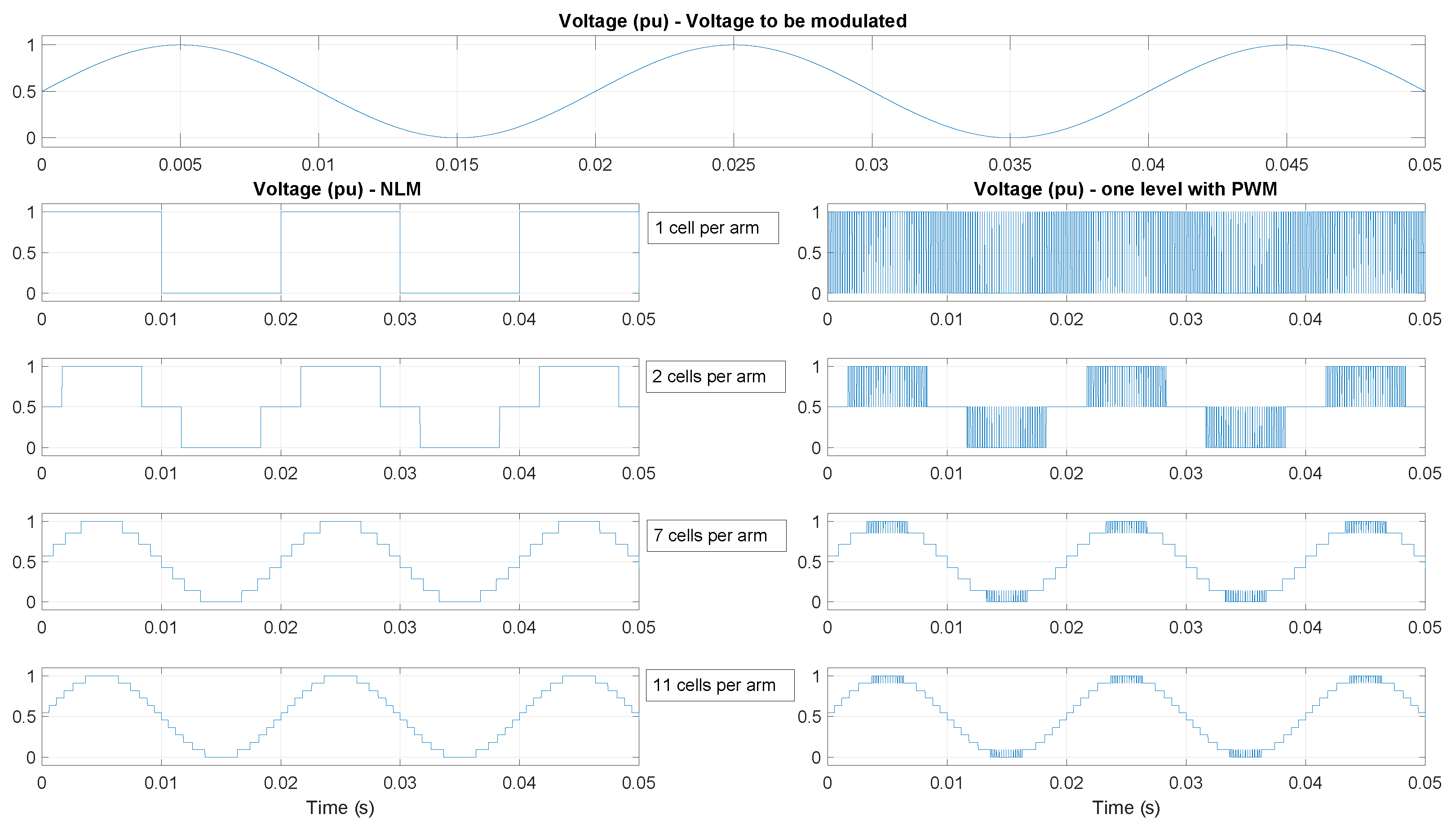
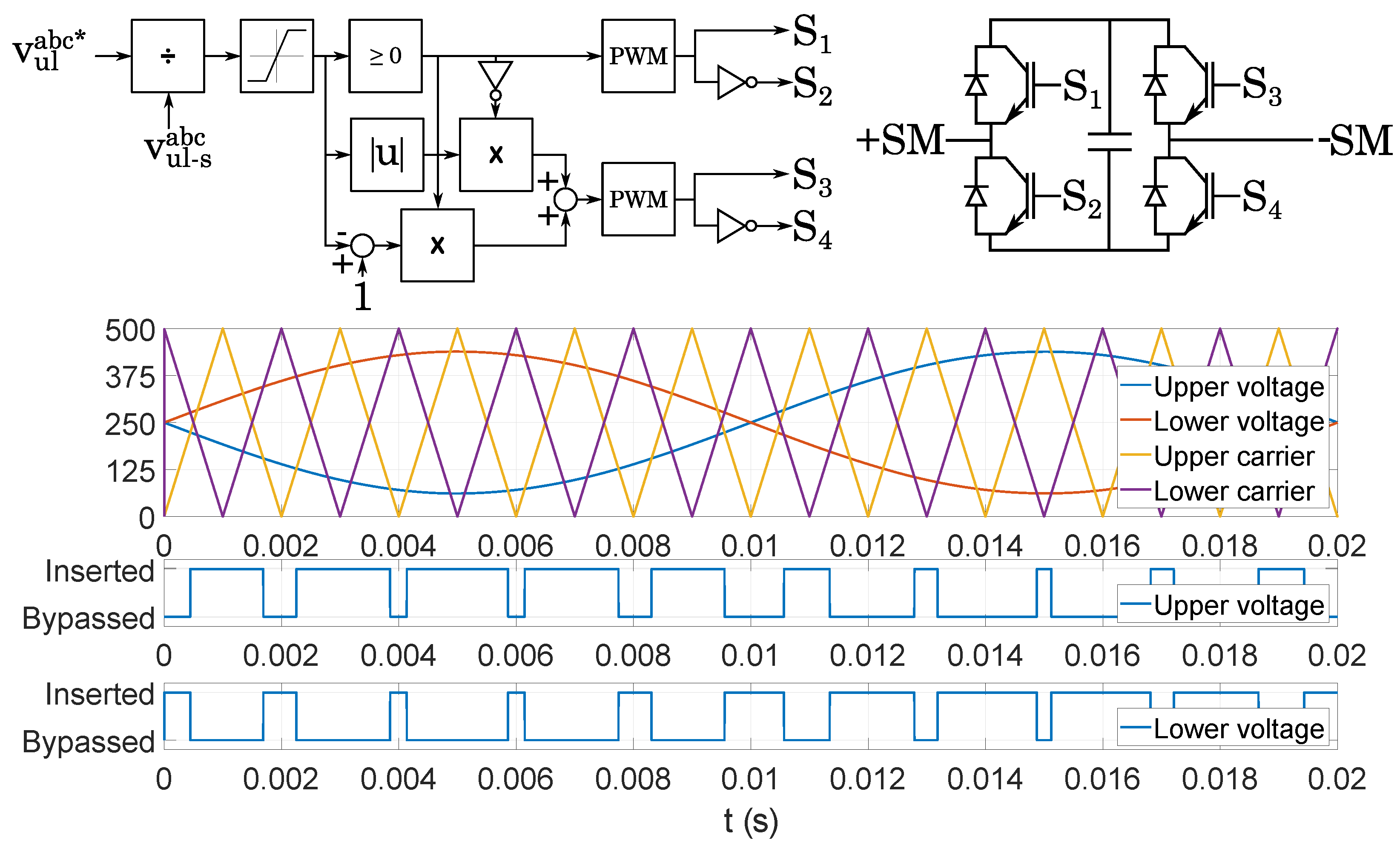
3.5. Cell Modulation

The proposed converter structure presents the possibility of connecting the positive and negative pole of the DC bus through the arm inductances depending on the switches states. Whenever this happens, arm inductances will limit the current and ensure the safe operation of the converter. As shown in Figure 9, the modulation technique has been designed with two carriers phase-shifted π rad to have anti-symmetric switching of the upper and lower arms. This is ensured in steady-state conditions, but when the converter is experiencing energy balancing transients, the switching of the upper and lower arms can lead to a direct connection. In this case, arm inductances secure the safe operation of the system, limiting the current inside the converter.

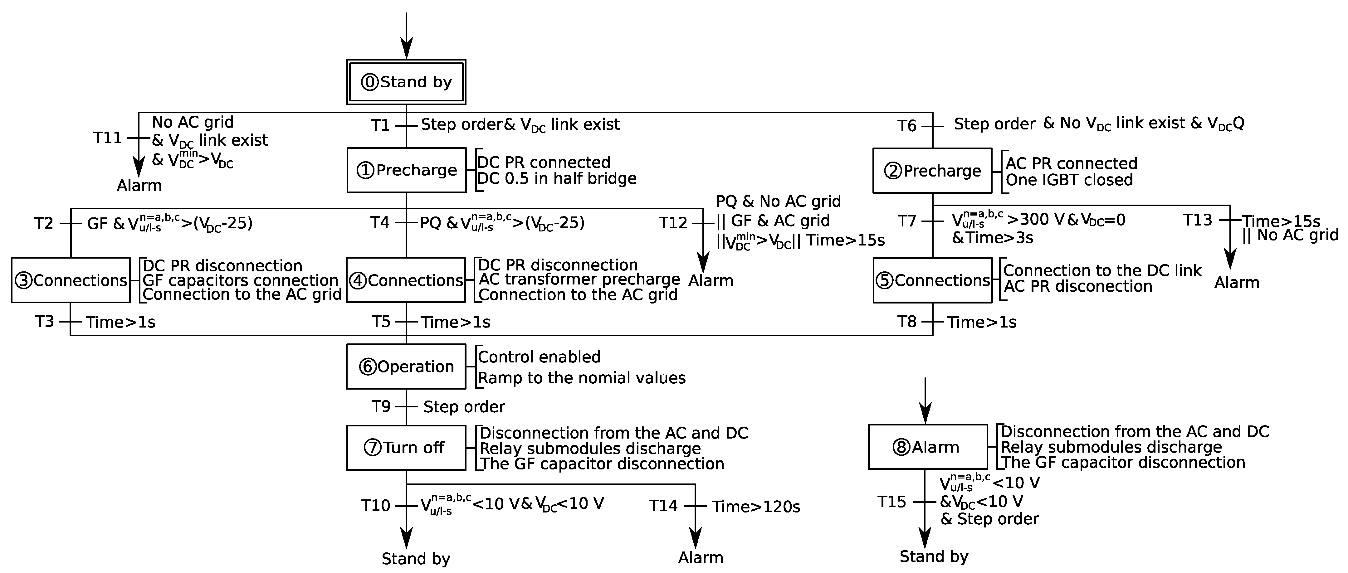
3.6. Start-Up and Shut-Down Sequences

In Figure 10 the start-up sequence is presented using GRAFCET approach, considering the different required sequences for the different system operation modes (grid-following PQ or VdcQ or grid forming). From the stand-by 🄋, a step order received as a communication signal begins the start-up sequence (T1 or T6). If the DC link has the right voltage (T1), it will be precharged from the DC side ①. If the DC link is discharged (T6), the precharge will be conducted from the AC grid ②. In the case that the precharge is carried out from the DC side ①, the DC preload resistances (PR) are connected. When the internal capacitors are charged approximately to the DC link voltage, the sequences passes to the next stage (③ or ④, depending on GF or PQ modes). If the grid-forming mode was set, the DC precharge resistance is disconnected, the grid-forming capacitors are connected, and the converter is connected to the AC grid ③. If the converter was set to PQ, the grid-forming capacitors are not needed, and the transformer must be energized ④. Then the converter is ready to start the operation ⑥. If the precharge is done from the AC grid, the converter must be set in VdcQ mode ②. In the precharge stage, the AC preload resistances are connected, and one IGBT is closed to let a half-bridge configuration. When the internal capacitors are charged to the phase-to-phase peak voltage, and there is no DC link, the converter passes to the next stage (⑤, after T7). In the connection stage ⑤, the converter is connected to the DC link, and the AC resistances are disconnected. Finally, the converter is ready for operation ⑥. When the converter is in the operation stage, the controls are enabled, and the converter control the capacitor voltage to the reference value. If there is a stop order (T9), then the converter disconnects from the AC grid, and the DC link and the cell relays are connected ⑦. When the converter is discharged the converter pass to stand by mode 🄋. In any of the stages of the sequence, if the alarm signal is activated, then the sequence moves to alarm state ⑧, where the converter is blocked.

4. Experimental and Simulation Results

4.1. Dynamic Simulation Model

The simulation models have been developed in PLECS [24] and it includes all the elements and IGBTs of the converter and the transformer. Discrete time controllers—identical to the physical ones in the converter—have been implemented in the simulations. The solver used is Radau (stiff) with variable step. The maximum step size has been set to 0.1 ms.

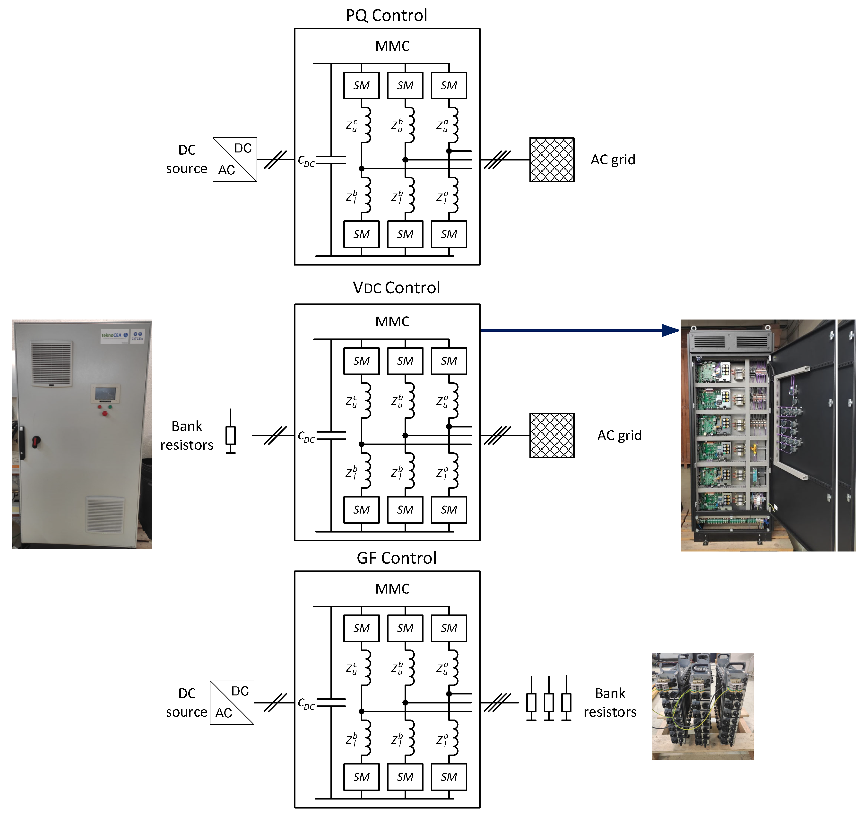
4.2. Experimental Setup Description

The setup scheme used to validate the MMC depends on the functional converter mode (PQ, VDC, GF). Figure 11 depicts the configurations to validate the different modes and the corresponding equipment used in the laboratory set-up. The DC source at the left side, MMC on the right side, and the configurable bank resistors at the bottom right side can be observed. PQ mode is validated by connecting the DC voltage source on the DC MMC converter side to emulate the DC link, and the grid is connected to the MMC AC side. However, VDC mode is validated connecting the MMC converter to the AC grid, and the configurable bank resistors are connected on the DC MMC side. Finally, the grid-forming mode (GF) is validated connecting the DC voltage source on the DC MMC converter side and the configurable bank resistors on the AC MMC side.
The following subsection include the experimental and simulation results conducted to validate the proposed concept.

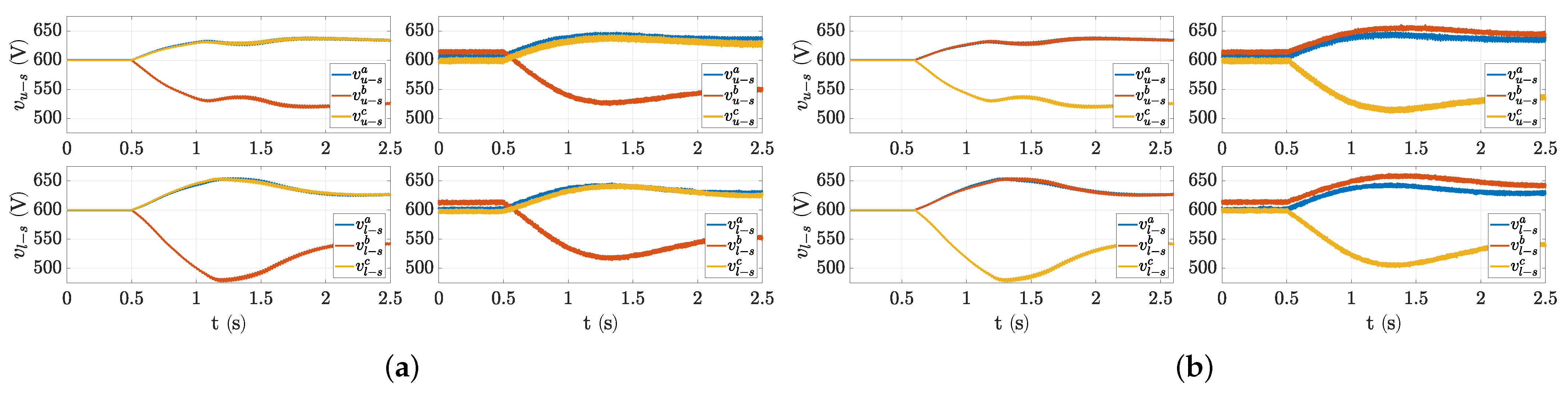
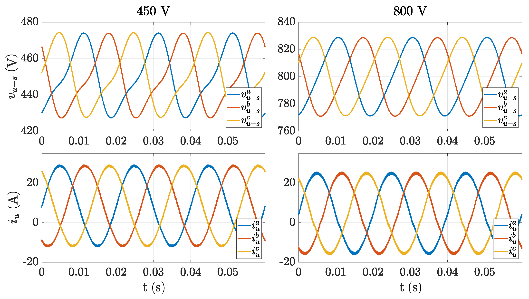
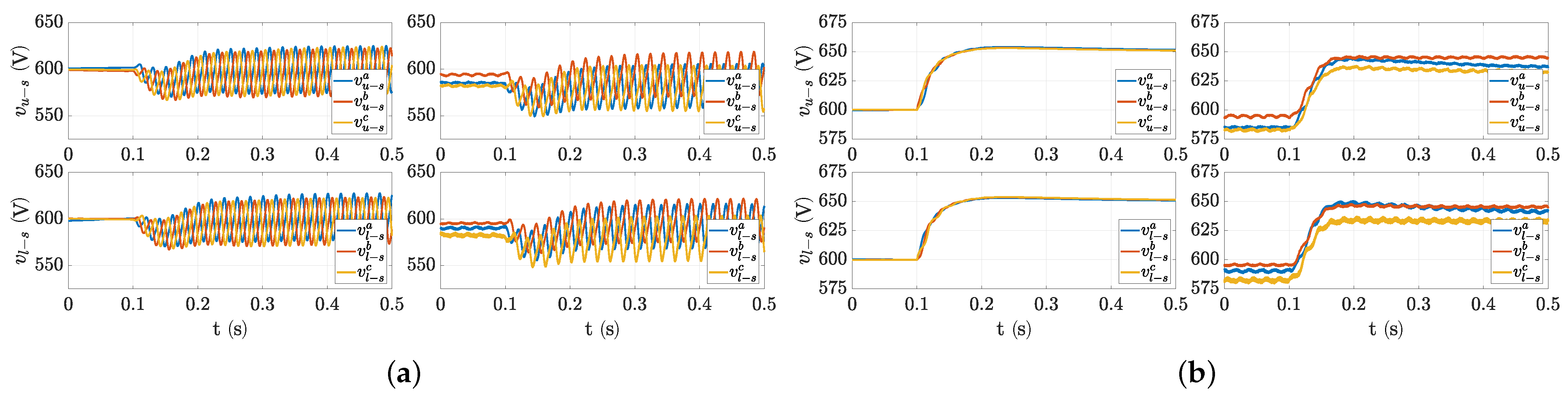
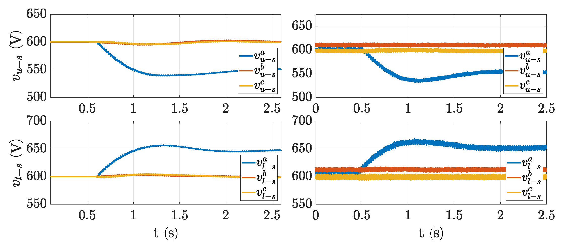
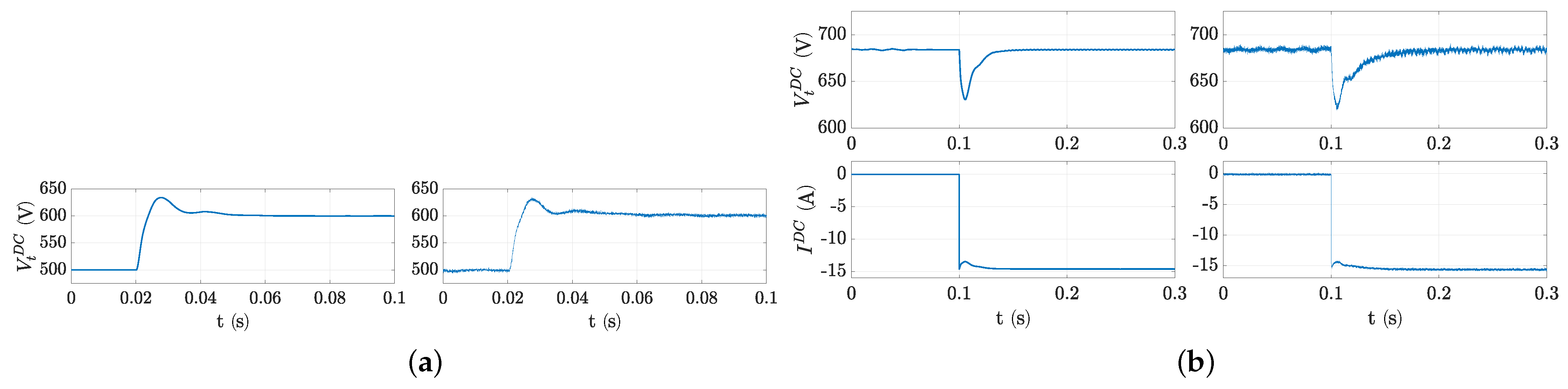
4.3. Validation of Cell Energy Controllers

Different tests have been considered to validate the internal energy control. The power set point has been changed from 0 to 1 pu Figure 12 shows experimental and simulation results of the evolution of the arm lower and upper cells voltages for two example cases. The DC voltage set-point has been changed from 600 to 650 V and the energy difference between phases has been changed from 0 to 120 J. Figure 13 shows experimental and simulation results for two example cases.The phase A energy difference between upper and lower arms has been changed from 0 to 60 J. Figure 14 shows experimental and simulation results.

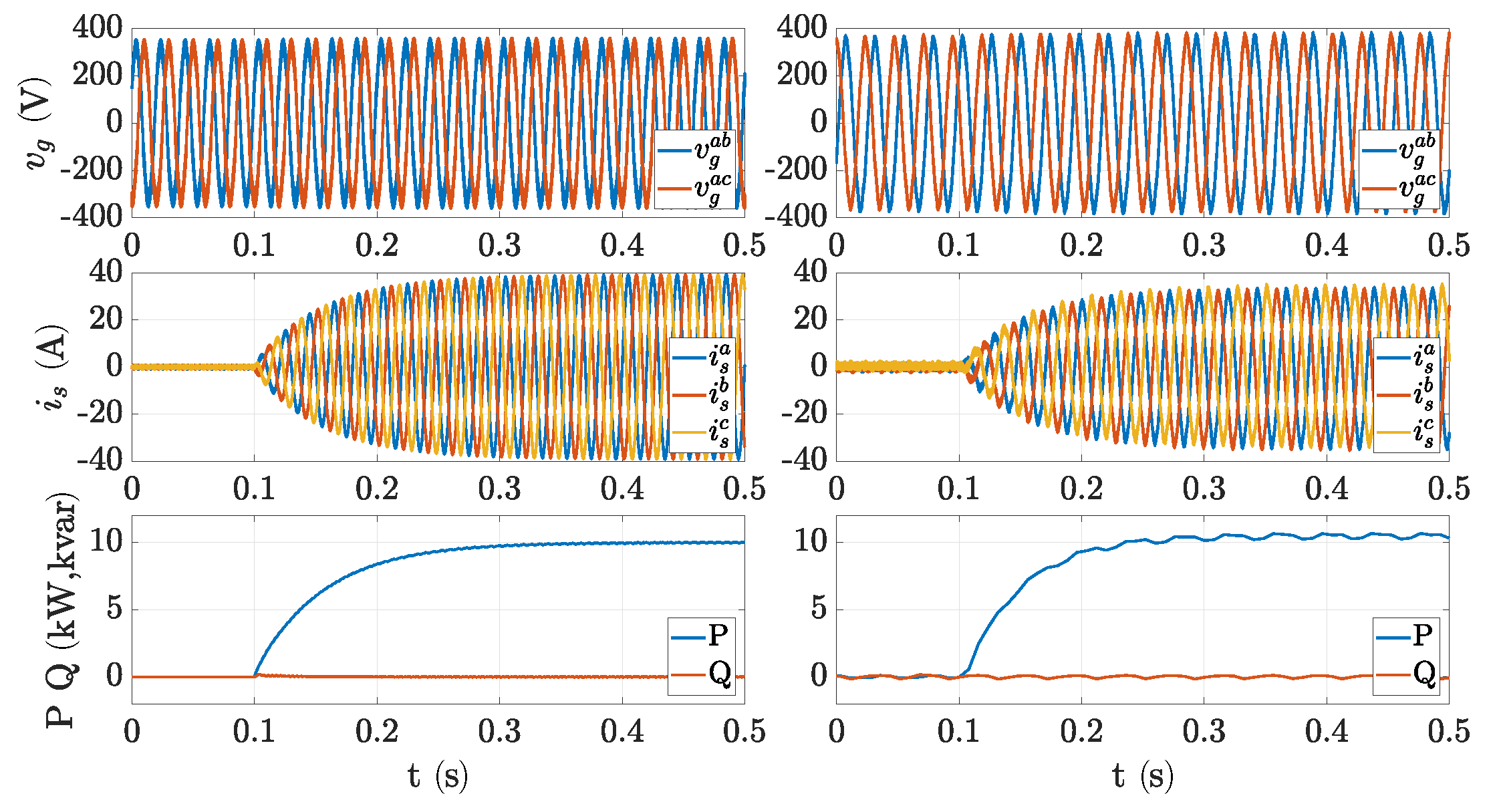
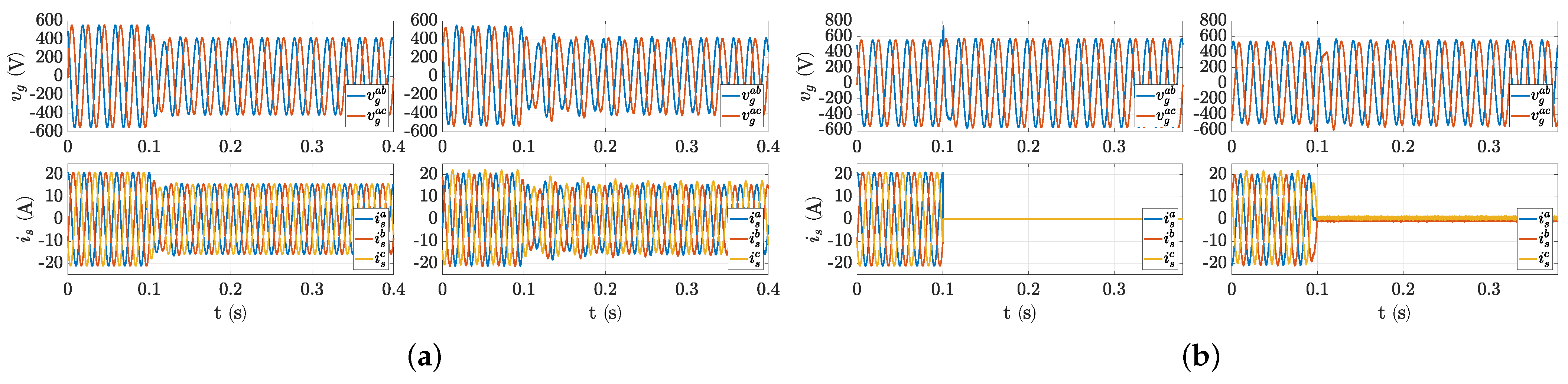
4.4. Validation of MMC Converter Grid-Following PQ, VdcQ and Grid-Forming Control

Reference tracking of the active and reactive power controllers has been tested. Both control loops have been designed to have a first-order response with a time constant of 50 ms. As an example, Figure 15 shows experimental and simulation results of a step change from 0 to the maximum active power (10 kW).
The Vdc control has been tested in grid-following mode, analyzing the Vdc reference tracking and the rejection of power disturbances in the DC side. Figure 16 shown experimental and simulation results of a DC voltage reference change and the response to a sudden connection of DC resistors in the DC side (10 kW).
Grid forming control has been validated, by testing changes in the reference of the AC voltage or frequency reference and also the response to sudden changes in the load (Figure 17 shows experimental and simulation results).

5. Discussion

The results presented above show that the proposed converter can include all the relevant controllers existing in an MMC, such as the energy control (which allows AC and DC power to be uncoupled) and the arm voltage control (which enables the balancing between arms ), as shown in Section 4.3. In addition, it can have the same outer controls as shown in Section 4.4. The control that cannot be applied is the NLM, which also cannot be applied in the other converters presented in the literature [3,5,6,7,8,9,10,11,12,13,14,15,16,17,18,19,20].
The proposed converter is the simpler and lowest cost converter structure that can include all the relevant controllers existing in an MMC. It is simpler since it only has one submodule per arm. Then, it does not need to balance the energy inside the arm and reduces the communications needed. Furthermore, having only one submodule per arm is cheaper since fewer power electronics are needed. A comparison between the proposed converter, MMC, other prototypes presented in the literature and the two-level VSC is carried on in Table 1 and in Figure 18.

6. Conclusions

The paper has proposed a new MMC concept, based on arms with a single cell. The proposed converters allow the formulation of the simplest possible converter that maintains the fundamental structure of an MMC. The converter includes all the inner controllers of large scale HVDC MMCs, except for the converter modulation, where PWM is used instead of NLM, which is commonly used in high-voltage applications with a sufficiently large number of cells. The paper has included the design and construction of the converter and has elaborated on how the different design decisions have been made. The converter controllers have been presented also discussing on aspects related to the practical implementation, including measurements and communications. Finally, the paper has presented some of tests conducted with dynamic simulations and experimentally to test different converter functionalities.

Author Contributions

Conceptualization, J.G.-B., O.G.-B. and E.P.-A.; methodology, J.G.-B., O.G.-B. and T.L.-P.; software, J.G.-B., T.L.-P. and M.C.-L.; validation, J.G.-B., T.L.-P., M.C.-L., C.C.-R., N.A.C. and O.S.-R.; investigation, J.G.-B., T.L.-P., M.C.-L. and C.C.-R.; resources, M.P.; writing—original draft preparation, J.G.-B., O.G.-B., T.L.-P., M.C.-L. and C.C.-R.; writing—review and editing, J.G.-B., O.G.-B., T.L.-P., M.C.-L. and C.C.-R.; supervision, O.G.-B., T.L.-P., N.A.C., O.S.-R., D.M.-M., D.H.-P. and E.P.-A.; project administration, O.G.-B., T.L.-P., N.A.C. and O.S.-R.; funding acquisition, O.G.-B. and N.A.C. All authors have read and agreed to the published version of the manuscript.

Funding

This work was supported in part by FEDER/Ministerio de Ciencia, Innovación y Universidades—Agencia Estatal de Investigación, Project RTI2018-095429-B-I00 and in part by FI-AGAUR Research Fellowship Program, Generalitat de Catalunya. E. Prieto is a Serra Húnter lecturer. The work of Oriol Gomis-Bellmunt is supported by ICREA Academia. Part of the development was funded by DTU Wind Energy, Technical University of Denmark.

Institutional Review Board Statement

Not applicable.

Informed Consent Statement

Not applicable.

Data Availability Statement

Not applicable.

Conflicts of Interest

The authors declare no conflict of interest.

Abbreviations

The following abbreviations are used in this manuscript:
MMCmodular multilevel converters
HVDChigh-voltage direct current
STATCOMstatic synchronous compensator
NLMnearest level modulation
PWMpulse width modulation
FACTSflexible alternating current transmission system
VSCvoltage source converter
ACalternating current
DCdirect current
LCCline commutated converter
IGBTinsulated gate bipolar transistor
HMIhuman–machine interface
PTPprecision time protocol
CANcontroller area network
PLLphase locked loop
PRpreload resistances
GFgrid forming
SMsubmodule

References

  1. Sharifabadi, S.; Harnefors, L.; Nee, H.; Norrga, S.; Teodorrescu, R. Design, Control, and Application of Modular Multilevel Converters for HVDC Transmission Systems; Wiley: Hoboken, NJ, USA, 2016; 412p. [Google Scholar]
  2. Van Hertem, D.; Gomis-Bellmunt, O.; Liang, J. HVDC Grids: For Offshore and Supergrid of the Future; Wiley: Hoboken, NJ, USA, 2016; pp. 3–24. [Google Scholar] [CrossRef]
  3. Zhang, H.; Belhaouane, M.M.; Colas, F.; Kadri, R.; Gruson, F.; Guillaud, X. On Comprehensive Description and Analysis of MMC Control Design: Simulation and Experimental Study. IEEE Trans. Power Deliv. 2021, 36, 244–253. [Google Scholar] [CrossRef]
  4. Prieto-Araujo, E.; Junyent-Ferré, A.; Collados-Rodríguez, C.; Clariana-Colet, G.; Gomis-Bellmunt, O. Control design of Modular Multilevel Converters in normal and AC fault conditions for HVDC grids. Electr. Power Syst. Res. 2017, 152, 424–437. [Google Scholar] [CrossRef] [Green Version]
  5. Judge, P.D.; Chaffey, G.; Merlin, M.M.; Clemow, P.R.; Green, T.C. Dimensioning and modulation index selection for the hybrid modular multilevel converter. IEEE Trans. Power Electron. 2018, 33, 3837–3851. [Google Scholar] [CrossRef] [Green Version]
  6. Li, Z.; Wang, P.; Chu, Z.; Zhu, H.; Luo, Y.; Li, Y. An inner current suppressing method for modular multilevel converters. IEEE Trans. Power Electron. 2013, 28, 4873–4879. [Google Scholar] [CrossRef]
  7. Hagiwara, M.; Akagi, H. Control and Experiment of Pulsewidth-Modulated Modular Multilevel Converters. IEEE Trans. Power Electron. 2009, 24, 1737–1746. [Google Scholar] [CrossRef]
  8. Zhong, Y.; Roscoe, N.; Holliday, D.; Lim, T.C.; Finney, S.J. High-Efficiency mosfet-Based MMC Design for LVDC Distribution Systems. IEEE Trans. Ind. Appl. 2018, 54, 321–334. [Google Scholar] [CrossRef]
  9. Ilves, K.; Antonopoulos, A.; Norrga, S.; Nee, H.P. A new modulation method for the modular multilevel converter allowing fundamental switching frequency. IEEE Trans. Power Electron. 2012, 27, 3482–3494. [Google Scholar] [CrossRef]
  10. Peftitsis, D.; Tolstoy, G.; Antonopoulos, A.; Rabkowski, J.; Lim, J.K.; Bakowski, M.; Ängquist, L.; Nee, H.P. High-power modular multilevel converters with SiC JFETs. IEEE Trans. Power Electron. 2012, 27, 28–36. [Google Scholar] [CrossRef] [Green Version]
  11. Moranchel, M.; Sanchez, F.M.; Bueno, E.J.; Rodriguez, F.J.; Sanz, I. Six-level modular multilevel converter prototype with centralized hardware platform controller. In Proceedings of the IECON 2015—41st Annual Conference of the IEEE Industrial Electronics Society, Yokohama, Japan, 9–12 November 2015; pp. 3863–3868. [Google Scholar] [CrossRef]
  12. Quraan, M.; Tricoli, P.; D’Arco, S.; Piegari, L. Efficiency Assessment of Modular Multilevel Converters for Battery Electric Vehicles. IEEE Trans. Power Electron. 2017, 32, 2041–2051. [Google Scholar] [CrossRef]
  13. Yang, L.; Li, Y.; Li, Z.; Wang, P.; Xu, S.; Gou, R. Loss Optimization of MMC by Second-Order Harmonic Circulating Current Injection. IEEE Trans. Power Electron. 2018, 33, 5739–5753. [Google Scholar] [CrossRef]
  14. Zhang, Y.; Wang, H.; Wang, Z.; Blaabjerg, F.; Saeedifard, M. System-level power loss evaluation of modular multilevel converters. In Proceedings of the 2019 IEEE Energy Conversion Congress and Exposition, ECCE 2019, Baltimore, MD, USA, 29 September–3 October 2019; pp. 6797–6804. [Google Scholar] [CrossRef]
  15. Taffese, A.A.; De Jong, E.; D’Arco, S.; Tedeschi, E. Online Parameter Adjustment Method for Arm Voltage Estimation of the Modular Multilevel Converter. IEEE Trans. Power Electron. 2019, 34, 12491–12503. [Google Scholar] [CrossRef]
  16. Liu, Z.; Li, K.; Sun, Y.; Wang, J.; Wang, Z.; Sun, K.; Wang, M. A Steady-State Analysis Method for Modular Multilevel Converters Connected to Permanent Magnet Synchronous Generator-Based Wind Energy Conversion Systems. Energies 2018, 11, 461. [Google Scholar] [CrossRef] [Green Version]
  17. Cheng, Q.; Wang, C.; Wang, J. Analysis on Displacement Angle of Phase-Shifted Carrier PWM for Modular Multilevel Converter. Energies 2020, 13, 6743. [Google Scholar] [CrossRef]
  18. Wang, S.; Alsokhiry, F.S.; Adam, G.P. Impact of Submodule Faults on the Performance of Modular Multilevel Converters. Energies 2020, 13, 4089. [Google Scholar] [CrossRef]
  19. Wu, W.; Wu, X.; Yin, J.; Jing, L.; Wang, S.; Li, J. Characteristic Analysis and Fault-Tolerant Control of Circulating Current for Modular Multilevel Converters under Sub-Module Faults. Energies 2017, 10, 1827. [Google Scholar] [CrossRef] [Green Version]
  20. Ma, Y.; Lin, H.; Wang, Z.; Ze, Z. Modified State-of-Charge Balancing Control of Modular Multilevel Converter with Integrated Battery Energy Storage System. Energies 2019, 12, 96. [Google Scholar] [CrossRef] [Green Version]
  21. TeknoCEA. PCO-10T800 Brochure. 2015. Available online: https://www.teknocea.cat/file/95a1828740ccf46486c48efd0c0442827d5f8c7e/MAS_BRO_PCO-10T800v3_R1_2015_09_03.pdf (accessed on 17 December 2020).
  22. TeknoCEA. CDA01-CU3 Brochure. 2015. Available online: https://teknocea.cat (accessed on 17 December 2020).
  23. Sánchez-Sánchez, E.; Prieto-Araujo, E.; Junyent-Ferré, A.; Gomis-Bellmunt, O. Analysis of MMC Energy-Based Control Structures for VSC-HVDC Links. IEEE J. Emerg. Sel. Top. Power Electron. 2018, 6, 1065–1076. [Google Scholar] [CrossRef] [Green Version]
  24. Alimeling, J.H.; Hammer, W.P. PLECS-piece-wise linear electrical circuit simulation for Simulink. In Proceedings of the IEEE 1999 International Conference on Power Electronics and Drive Systems, PEDS’99 (Cat. No.99TH8475), Hong Kong, China, 27–29 July 1999; Volume 1, pp. 355–360. [Google Scholar] [CrossRef]
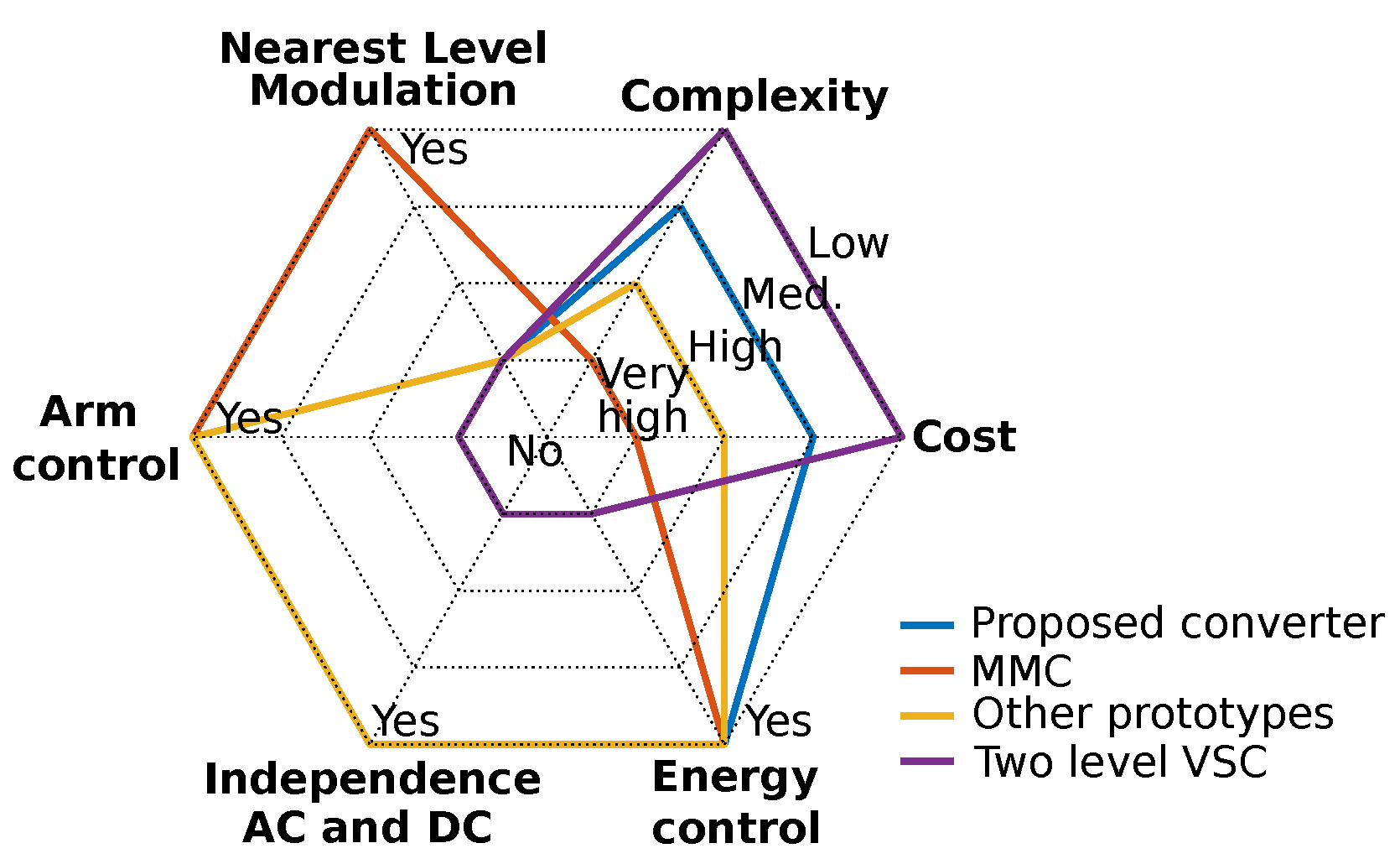
Figure 1. Typical modular multilevel converter scheme.
Energies 15 01819 g001
Figure 2. Example of NLM modulation and hybrid NLM-PWN modulation (PWM in only one cell per arm).
Energies 15 01819 g002
Figure 3. Scheme of the proposed modular multilevel converter with one cell per arm (half-bridge and full-bridge versions).
Energies 15 01819 g003
Figure 4. Single-line diagram of the converter and image of the assembled system. Front view (left) and rear view (right).
Energies 15 01819 g004
Figure 5. Cell voltages and arm currents.
Energies 15 01819 g005
Figure 6. Overall scheme of the converter measurements, driving signals and communications.
Energies 15 01819 g006
Figure 7. Overall MMC control structure.
Energies 15 01819 g007
Figure 8. General converter control scheme including grid-forming and grid-following control modes.
Energies 15 01819 g008
Figure 9. Modulation logic implemented and example results.
Energies 15 01819 g009
Figure 10. Start-up sequence GRAFCET.
Energies 15 01819 g010
Figure 11. General setup employed for testing the converter.
Energies 15 01819 g011
Figure 12. Simulation (left) and experimental (right) results, (a) showing capacitors (arm) voltage during a step change is applied to P from 0 to 1 pu (b) showing capacitors (arm cells) voltage during a step from 600 V to 650 V in the arms capacitors voltage.
Energies 15 01819 g012
Figure 13. Simulation (left) and experimental (right) results, showing capacitors (arm cells) voltage during a step from 0 J (normal operation) to 120 J is applied to the energy difference between phase A and phase B (a) and between phase A and C (b).
Energies 15 01819 g013
Figure 14. Simulation (left) and experimental (right) results, showing capacitors (arm cells) voltage during a step from 0 J (normal op.) to 60 J is applied to the energy difference between the upper and lower arms of phase A.
Energies 15 01819 g014
Figure 15. Simulation (left) and experimental (right) results, showing AC grid voltages, currents and powers for a step in P from 0 to 10 kW.
Energies 15 01819 g015
Figure 16. Simulation (left) and experimental (right) results, (a) showing the DC link voltage during a step change from 500 V to 600 V. (b) showing the DC voltage and current when a R equivalent to rated power (10 kW) is connected.
Energies 15 01819 g016
Figure 17. Simulation (left) and experimental (right) results, (a) showing AC grid voltage and current when a step change from 400 V to 300 V. (b) showing AC grid voltage and current when a resistance equivalent to the rated power (10 kW) is disconnected from the AC grid.
Energies 15 01819 g017
Figure 18. Spider plot comparison between the proposed converter, MMC, other prototypes and the two-level VSC.
Energies 15 01819 g018
Table 1. Comparison between different converters.
Proposed ConverterMMCOther Prototypes Presented [3,5,6,7,8,9,10,11,12,13,14,15,16,17,18,19,20]Two-Level VSC
ComplexityMediumVery highHighLow
CostMediumVery highHighLow
Energy controlYesYesYesNo
Independence between AC and DC powerYesYesYesNo
Arm voltage controlYesYesYesNo
Nearest Level ModulationNoYesNoNo
Publisher’s Note: MDPI stays neutral with regard to jurisdictional claims in published maps and institutional affiliations.

