Abstract
Light-emitting diodes based on quantum dots as an active emission can be considered as a promising next generation for application in displays and lighting. We report a theoretical investigation of green emission at 550 nm of microcavity inorganic–organic light-emitting devices based on Zn (Te, Se) alloy quantum dots as an active layer. Distributed Bragg Reflector (DBR) has been applied as a bottom mirror. The realization of high-quality DBR consisting of both high and low refractive index structures is investigated. The structures applied for high refractive index layers are (ZrO2, SiNx, ZnS), while those applied for low index layers are (Zr, SiO2, CaF2). DBR of ZnS/CaF2 consisting of three pairs with a high refractive index step of ( = 0.95) revealed a broad stop bandwidth (178 nm) and achieved a high reflectivity of 0.914.
1. Introduction
Quantum dots (QDs) have a unique property that originates almost individually due to the size regime in which they exist. The unique optical properties of quantum dots take place because of the quantum confinement effect [1]. The current study focused on wide bandgap II-VI semiconductors quantum dots because of their fundamental structural, electrical, and distinguished optical properties [2].
Zn (Te, Se) ternary alloy QDs are considered one of the essential types of II–VI semiconductors that possess favorable optical properties, as they displayed tunable and narrow-band photoluminescence (PL) emission [3,4].
Zn (Te, Se) is considered a good candidate for Cd-free and green emission materials with a long lifetime. The existence of the green band emission of Zn (Te, Se) partially results from the combination of ZnTe QDs and Te isoelectronic centers in ZnSe. The fact that ZnTe quantum dots as a partial source of green emission was confirmed by the power-dependent PL spectra. In addition, a long lifetime of the PL emission arises from the alignment of the type-II band between ZnSe and ZnTe [5]. The electrons from the conduction band in ZnSe and holes from the valence band in ZnTe were involved in the recombination process, leading to a smaller energy bandgap than that of either of ZnTe or ZnSe.
The energy of the bandgap of an alloyed system such as Zn (Te, Se), which consists of materials with considerably numerous chemical features and lattice constants, exhibited a significant negative deviation from the mean of the bandgap mole fraction weighted. Therefore, the Zn (Te, Se) system is named a highly mismatched semiconductor alloy [6]. The band gaps of this alloy possess much smaller energies than their constituents of unalloyed materials. The band gaps of ZnTe and ZnSe, are, respectively, 2.25 and 2.72 [7], while the minimal energy of the bandgap of the Zn (Te, Se) alloy is considered to be 2.03 eV at Zn (Te0.63Se0.37) [8]. Thus, the green emission of Zn (Te1−xSex) QDs can be realized by controlling their particle size and composition [3].
It is worth mentioning the importance of semiconductor nanocrystals generated from their unique size-dependent optical and electrical properties, which can be utilized in constructing optoelectronic devices [9]. Therefore, semiconductor nanostructures are promising for application as a pure source of monochrome light-emitting diodes [10]. Light-emitting devices based on organic and inorganic structures with electrically excited quantum dots have experienced a large development. This type of configuration becomes competitive to the organic light-emitting devices for the application in displays because of their unique outstanding features of simple solution processability, tunable emission color with high saturation, and high brightness [11,12].
This paper demonstrates the realization of bottom green emission of QD-organic light emitting devices (QD-OLED) by using Distributed Bragg Reflector (DBR) as an optical reflector. The DBR is characterized by having a periodic structure with alternating dielectric layers. Therefore, it can be utilized to afford a high degree of reflection in a certain range of wavelengths by manipulating the thickness and differences in the refractive indexes of the dielectric layers [13]. DBR mirrors have high reflectivity and a small intrinsic absorption coefficient. The high reflectivity of light comes from the constructive interference between the incident light and the reflected light due to Fresnel reflection. The utilization of high-purity dielectric material leads to the production of highly efficient DBR mirrors. It suppresses absorption and controls the thickness of layers during fabrication, leading to obtaining the desired reflection wavelength [14]. According to these features, DBRs can be used in photovoltaic devices [15], vertical-cavity surface-emitting lasers (VCSELs) [16], light-emitting diodes (LEDs) [17], and solar cell actuators [18]. Furthermore, DBR is sensitive toward electric, magnetic, mechanic, and chemical stimuli, giving various characters to be used in different applications [19].
Kitabayashi and co-workers fabricated OLED with ZnS/CaF2 DBR with different pairs and evaluated their reflectance [20]. High-efficiency white OLED with ZrO2/Zr DBR investigated by Yonghua et al. [17]. In addition, Zhang and co-workers fabricated green OLEDs with ZrO2/Zr DBR by atomic layer deposition, and it was found that the ZrO2/Zr DBR structure significantly improves the light purity of green OLEDs without interfering with intrinsic electroluminescence properties [21].
In this work, we have attempted theoretically to compare the performance of green QD-OLED based on different types of DBRs. We have chosen the materials of DBRs with different index contrast to show the effect of this parameter on the performance of the devices. In addition, different pair numbers of DBRs were used to demonstrate the effect of this parameter on the performance of the devices. DBRs have been used as a bottom mirror for light-emitting devices based on organic and inorganic QD structures with green emission to investigate their microcavity effects on device performance. Zn (Te, Se) alloy QD with green emission at a wavelength of 550 nm has been applied as an active layer. The schematic structure of the designed device of QD-OLED with multilayered film at the bottom side are shown in Figure 1a. As shown in the figure, we used indium tin oxide (ITO)/DBR as a reflector anode. N,N′-Di(1-naphthyl)-N,N′-diphenyl-(1,1′-biphenyl)-4,4′-diamine (NPB) was used as the hole transport layer and ZnTeSe alloy QD as an emissive layer. Bis[2-(2-hydroxyphenyl)-pyridine]-beryllium (Bepp2) was used as the electron transport layer. Finally, Lithium quniolate (Liq) was used as an electron injection layer and Al as a cathode.
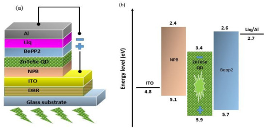
Figure 1.
(a) Schematic structure of device, (b) energy level diagram.
The investigation of light-emitting devices with green emission is very important for many applications, one of them that can be used as a source of illumination for oxygen saturation measurements in blood. Additionally, the green color has an important application in non-pharmacological therapy. Recent investigations proved that green light acts as a potential therapy in patients with episodic or chronic migraines with no side effects. It amended the number of headache days/months and improved the quality of life in both episodic and chronic migraine. In addition, the green light provides an additional therapy for the prevention of episodic and chronic migraine [22].
The energy-level diagram of the device is shown in Figure 1b. According to the energy-level diagram, the emission zone is confined to the QD layer due to good energy-level alignments at interfaces of adjacent layers.
2. Theoretical Analysis
2.1. Distributed Bragg Reflector
The most common OLED microcavity architectures incorporate two similar metal mirrors with variant thicknesses; one of them is fractional reflective. Another design includes one mirror with extreme reflection consisting of a dense dielectric distributed Bragg reflector (DBR) and other metal mirrors with low work function [17].
DBRs have tremendous relevance and acceptance in optoelectronic and photonic devices due to their high reflectance and wavelength selectivity compared to metallic mirrors [19]. DBR mirror contained alternating high and low refractive index layers of semiconductor compounds. The thickness of each of the layers is one-quarter wavelength (/4). The reflectivity of DBR is determined by the refractive index contrast and a number of periods [23].
A DBR mirror optical principle is based on successive Fresnel reflection at normal incidence at interfaces between two alternating layers with high and low refractive indices and respectively: . When each layer’s quarter wavelength (/4) optical thickness is maintained, the path difference between reflections from successive interfaces equals half of the wavelength (/2), or 180° out of phase. Despite the reflections (r) at successive interfaces having alternating signs, the 180° compensation phase shift can be obtained through the differences in path length, and all the reflected components interfere constructively. In this case, the cumulative reflection can be enhanced by changing the design. The transmission matrix theory has been used in calculating the reflectance spectrum of a DBR [24].
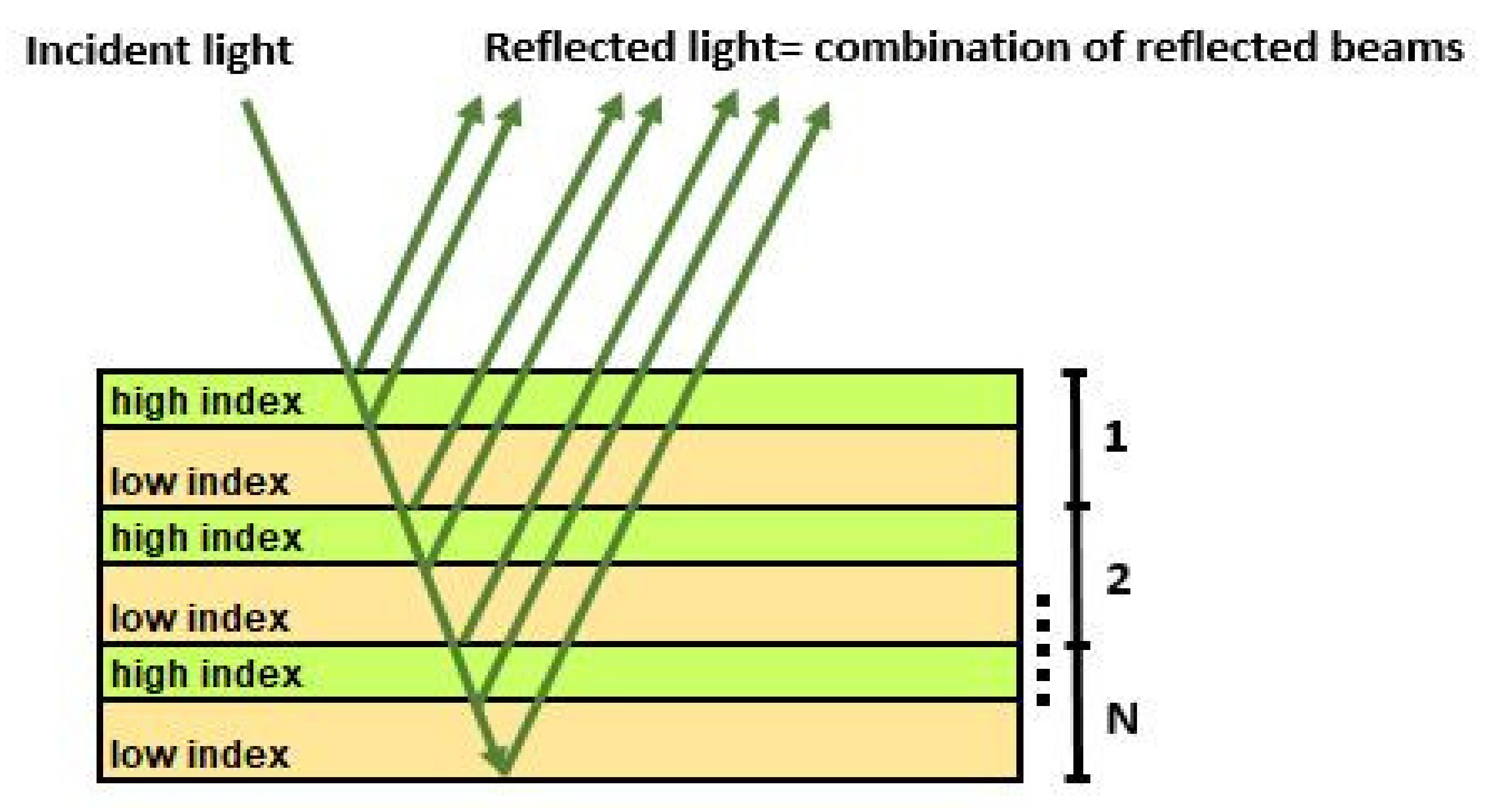
Reflected light from multiple films is due to the interference from the numerous lights reflected from each of the different surfaces. The interference of light reflected and transmitted by other contact surfaces of multiple film layers is depicted in the scheme shown in Figure 2 [25]. The structure is designed so that all reflected components from the interfaces interfere effectively, leading to a strong reflection. The range of wavelengths that are reflected is termed a photonic stopband. The stopband is controlled mainly by the index contrast of the two materials [19] that can be calculated by [24]:
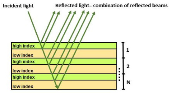
Figure 2.
Reflectance of DBR structure.
is proportional to the Bragg wavelength and is sensitively affected by the index contrast ( = ). Thus, the elevation in is very desirable in DBR fabrication for both a high peak reflectance and a wide stopband width.
2.2. Cavity Emission Characteristics
Based on the concept of interfaces, the most straightforward formula for the emission of light from the thin-film structure, including an emissive layer, can be developed into a method that explains the transmission of a Fabry–Perot resonator structure [26]. In this study, the microcavity was designed as shown in Figure 3 of a top mirror composed of (Bepp2, Liq, and Al) and a bottom mirror is consisting of (NPB, ITO, and DBR), with using ZnTeSe alloy QD as an active emission layer. The theoretical spectrum for external emission normal to the plane of the layers of the device can be calculated based on classical optics by the following equation [27]:
where Rt and Rb are the reflectivities of the top and bottom mirrors, respectively, L is the optical thickness of the cavity, is the free space emission intensity at wavelength and is the optical thickness between the emitting sublayer and top mirror. is the internal observation angle from the surface normal to the microcavity; and are the phase changes upon reflection to the effective reflectivities of and . According to Equation (3), the resonance condition to maximize luminance from a cavity is given by [26]:
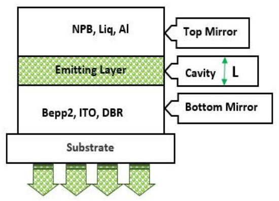
Figure 3.
Microcavity structure used for an optical analysis.
A measure of the quality of the resonance of the cavity is given by the finesse [28]. Finesse is described as the number of light oscillations between two mirrors at the free space wavelength (λ) before its energy decays by a factor of e−2π. A higher finesse exists as a result of a higher average number of times a photon is reflected back and forth within the cavity [29]. The finesse can be written in terms of reflectivity as follows [30]:
A cavity quality factor Q, which is defined as the reciprocal of the energy loss per cycle per energy stored in the cavity and may also be interpreted as the number of oscillations observed before decay below , can be expressed as [31]:
Cavity photon lifetime is a time constant that represents the rate at which photons are lost from the cavity and is given by [32],
where c is the speed of light.
Multilayer Calculation
The transfer matrix method (TMM) has been applied to calculate the reflection spectra for our devices; this method inherently included a standing wave enhancement effect and a multi-reflection with the optical cavity [33]. The electric fields, together with the magnetic field inside and outside multilayer structures, have been calculated using TMM, giving us the transmittance and reflectance of this kind of structure.
For homogeneous and isotropic multilayer structures, each layer is represented by a 2 × 2 matrix Mj of the form:
where μj is the optical admittance of j layer and δj is the phase change of the electromagnetic radiation traversing on the j layer and can be written as follows:
where nj is the refractive index of j layer, dj is the physical thickness of j layer and is the incidence angle at j layer; herein, a quarter wavelength is considered as the thickness of each layer to obtain the highest reflection [34].
The matrix relation defining the electric field (B) and magnetic field (C) of the multilayer structure adopted from [35] is as follows:
Using Equation (10) and considering the admittance introduced by the interfaces, which is indistinguishable from the reflectance, this idea has been applied for the reflectance calculation through the assembly of thin films. Then, the transmittance has been deduced from the reflectance R through T = 1 − R [36]. The reflectance R, transmittance T and the phase change on reflection Ψ are given by
where μ0 and μsub represent the optical admittance of the emission layer and substrate layer, respectively. Mathcad software has been used to compute the data needed for the calculations.
2.3. Quantum Dot Emission
In this work, we have investigated the effect of various structures of DBR bottom mirrors on the performance of emission at 550 nm wavelength. We have adopted an emission profile based on the published experimental results for ZnTeSe quantum dots for internal emission. The emission peak wavelength of the ZnTeSe alloy QD varied in the range from 530 to 579 nm by controlling the particle size in the range from 3.8 to 6.0 nm [3], the PL emission peak wavelength for of Zn(Te1−xSex) QDs with x = 0.24 ± 0.04 QDs with various diameters of 4.0, 4.2, 4.9 and 6.0 nm are 535, 540, 557 and 576 nm, respectively. The dependence of the emission peaks on the size of the quantum dots is presented in Figure 4. From these experimental data, an empirical fitting equation has been reproduced to express the relation between the diameter of QD (d) and the position of the emission peak wavelength P(d):
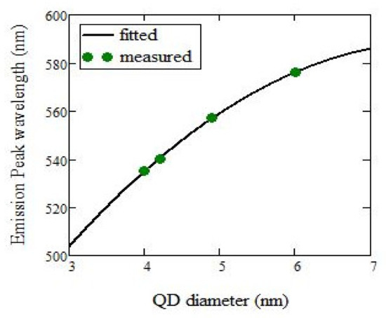
Figure 4.
Emission peak positions against QD size.
The QDs spontaneous emission, Eint(λ), is reproduced by adopting simulation using Gaussian distribution function, as follows:
where P is the position center of the peak and v was given by:
where Δλ is the full width at half maximum (FWHM) of QD emission. The FWHM of QD emission was assumed to be 30 nm [7]. According to Equation (14), the emission at 550 nm wavelength of ZnTeSe alloy QD is compatible with quantum dots with a diameter of 4.6 nm.
The refractive index and band gap of QD are the main properties that are changed by the size of QD. The refractive index of QD is calculated as follows [37,38]:
where is the refractive index of bulk material, the refractive index of bulk ZnTe and ZnSe at 550 nm are 3.1 and 2.7, respectively [39]. The calculated refractive index of ZnTeSe QD with diameter 4.6 nm for the emission at 550 nm is 2.748.
The shift of the optical band gap of QD due to quantum confinement has a quantitative form. According to an early effective mass model calculation by Brus, the magnitude of this confinement energy can be modeled as a particle in a box, as seen in Equation (18) [1].
where me is the effective mass of the electron, mh is the effective mass of the hole, is the reduced mass of the exciton system, and a is the radius of the quantum dot. For Zn (Te0.76Se0.24), me is 0.11 m0 and mh is 0.64 m0 (where m0 denotes the electron rest mass) [3]. The calculated optical band gap of Zn (Te, Se) alloy QD at 550 nm emission is approximately 2.5 eV, and this value is within the origin of the green band.
3. Results and Discussion
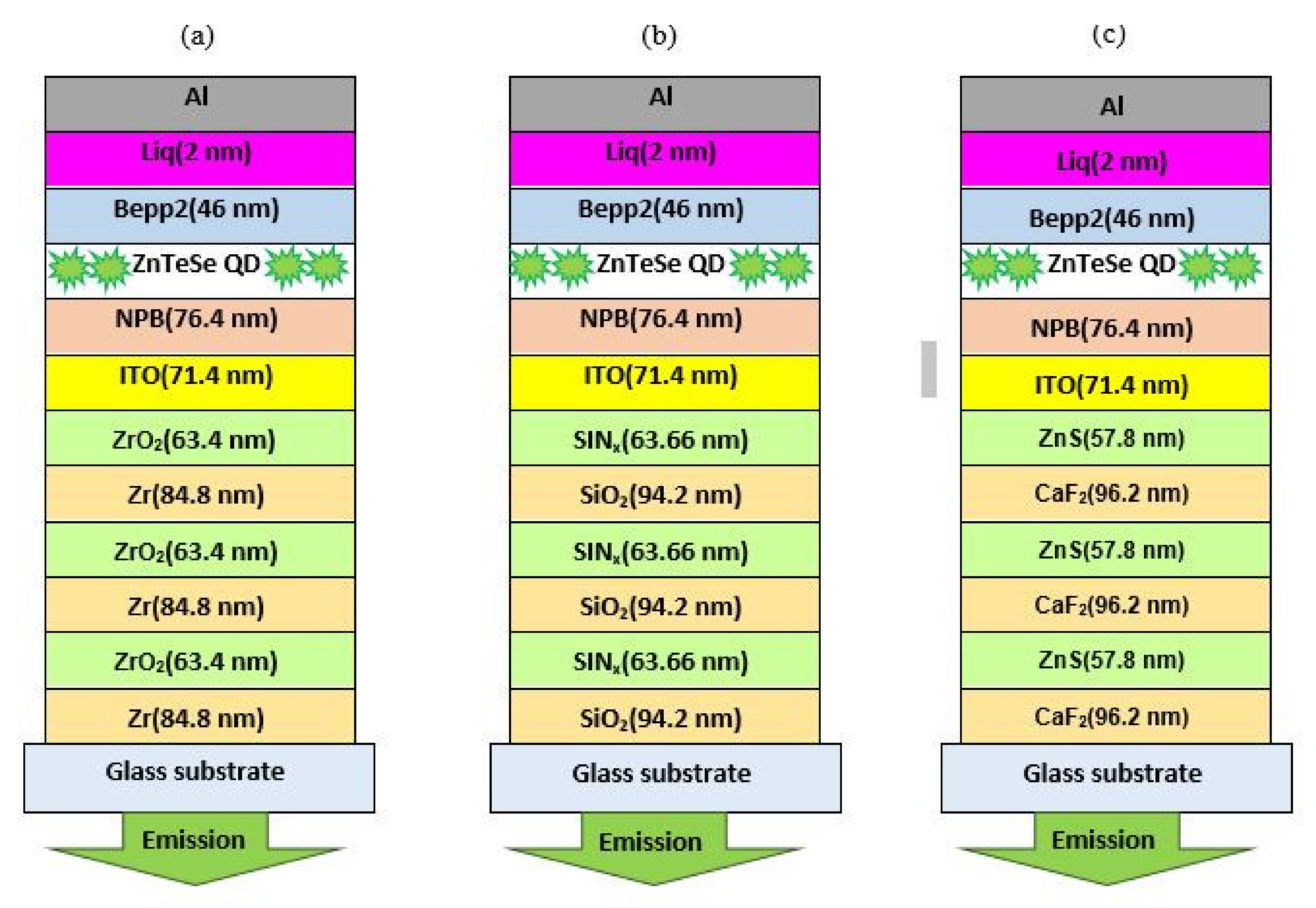
This study focuses on the use of a DBR as a bottom mirror; three DBRs labeled DBR1(ZrO2/Zr), DBR2 (SiNx/SiO2), and DBR3 (ZnS/CaF2) have been applied as bottom mirrors. (Zr, SiO2, CaF2) played as low refractive index materials, while (ZrO2, SiNx, ZnS) were used as high refractive index materials. Schematic-layer structures of ZnTeSe QD-OLED with three periods of DBR1, DBR2, and DBR3 are shown in Figure 5a–c, respectively. The thicknesses of all layers are also displayed in Figure 5. For designing the thickness of each layer in the DBRs, we have applied L = . According to the Bragg wavelength of 550 nm, and by using the refractive indices shown in Table 1, the thickness of multilayer films can be deduced as follows: the thicknesses of the ZrO2 and Zr of DBR1 are:
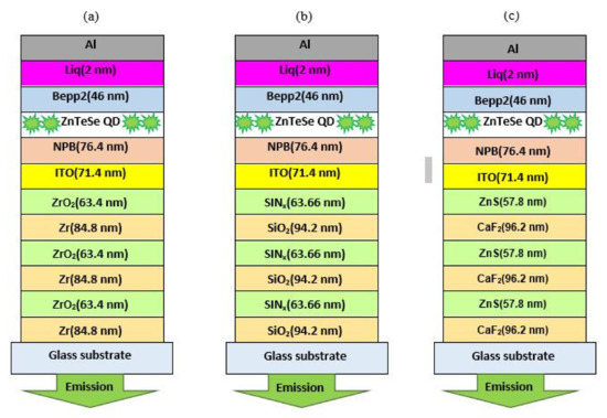
Figure 5.
Schematic layer structure of three devices at 550 nm based on (a) DBR1 (b) DBR2 (c) DBR3.

Table 1.
Refractive indexes of multilayer films at 550 nm.
The thicknesses of the SiNx and SiO2 of DBR2 are:
The thicknesses of the ZnS and CaF2 of DBR3 are:
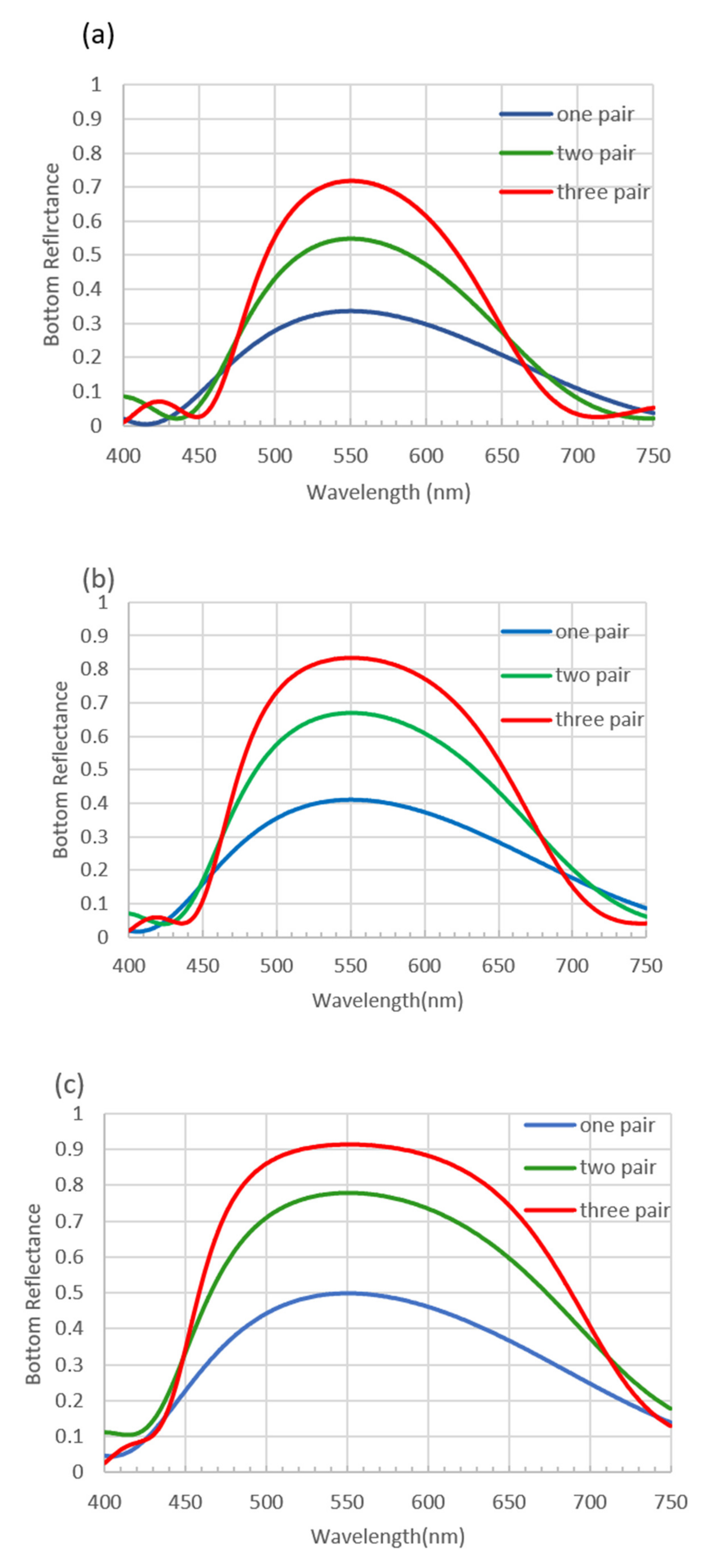
Three structures were designed with a variation of a number of periods of DBR from one to three. The reflectivities calculated by the transfer matrix model and their reflectance are displayed in Figure 6. The refractive index at 550 nm for ITO is 1.9251 + i0.0021684 [43], Al is 0.6 + i5.2745 [44], and the refractive index of organic materials is assumed to be 1.8. The main parameters that affect the performance of DBR are the number of periods (N) and index contrast (Δn). Therefore, the comparison of the performance of devices with emission at 550 nm based on different DBRs by changing (N) and (Δn) is estimated and tabulated in Table 2.
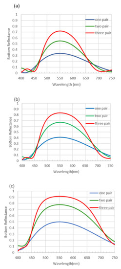
Figure 6.
Reflectance spectra by the number of pairs for devices based on (a) DBR1 (b) DBR2 (c) DBR3.
Table 2.
Comparison of the main characteristics for devices based on different designs of DBRs at 550 nm.
The main feature for the effect of variation of DBR periods can be observed in Figure 6. Clearly, the calculated reflectance seems to achieve higher values with the increasing number of DBR periods. In addition, the maximum reflectivity increased for DBR based on ZnS/CaF2, which has the highest (Δn) relative to DBRs consisting of ZrO2/Zr and SiNx/SiO2.
It is worth mentioning that the reflectivity of DBR3 with a number of periods equal to 2 is larger than that for the DBR1 with n = 3; this is because of the large differences between the values of index contrast. The values of for DBR1 and DBR3 are 0.55 and 0.95, respectively. Consequently, by using DBR3 consisting of ZnS/CaF2, we can obtain high reflectance and a wide stopband by applying a small number of periods. The decreasing number of periods has many scientific and economic benefits, such as avoiding scattering losses and saving time and materials.
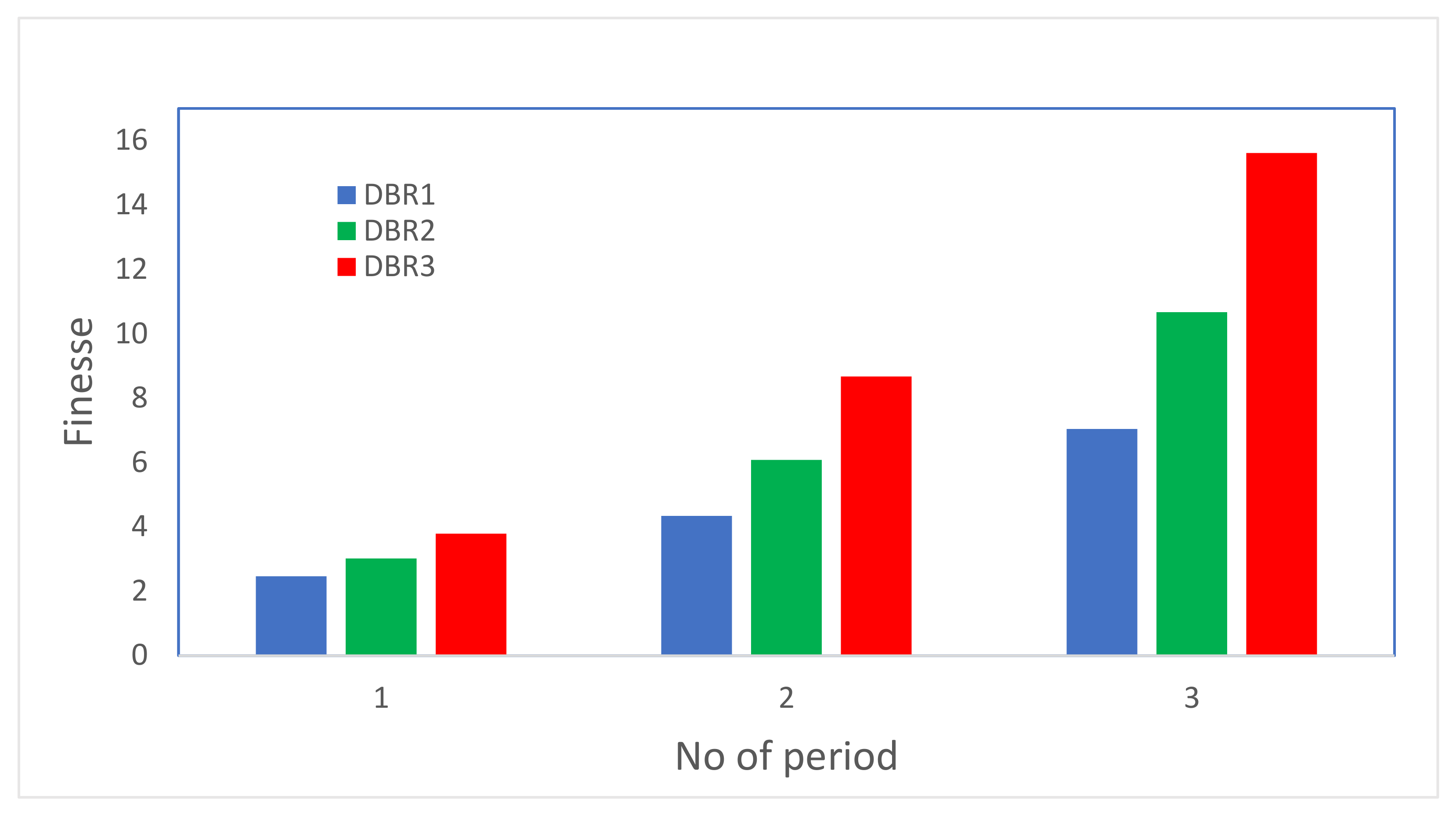
The calculated finesses of DBR structures with a varying number of periods are presented in Table 2. Figure 7 shows the finesse as a function of a number of DBR periods for three configurations applied in this work; the finesse increases with an increasing number of periods for the three devices with various DBR structures; additionally, the highest finesse (15.613) was found for DBR3 with three periods due it is the highest reflectivity of (0.914).
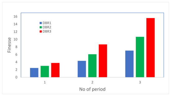
Figure 7.
Calculated finesse versus number of DBR periods for devices based on (DBR1, DBR2, and DBR3).
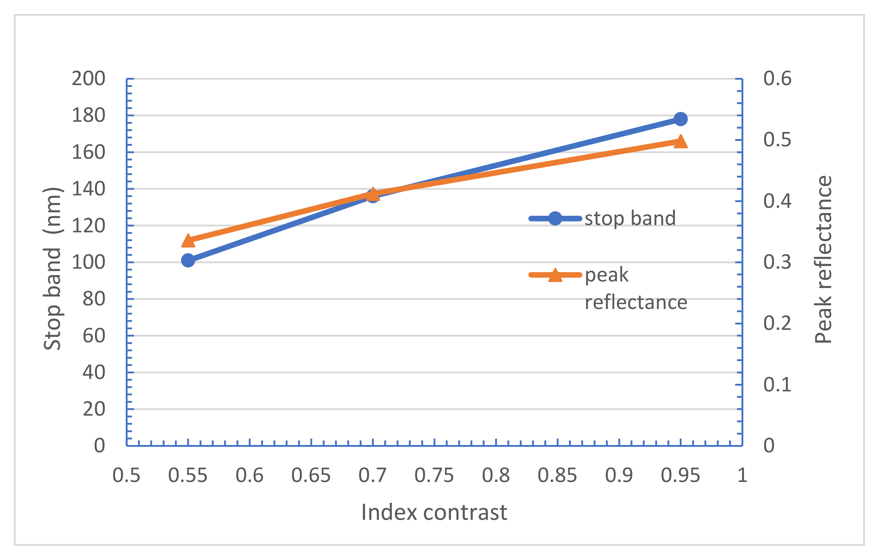
The graph of stopband against index contrast is shown in Figure 8. Obviously, the increase in index contrast leads to an increase in the stopband width, reaching 178. CaF2 clearly exhibits a smaller refractive index than ZnS, leading to a high index contrast (Δn = 0.95) compared to SiNx/SiO2 (Δn = 0.7) and ZrO2/Zr (Δn = 0.55), as reported in Table 2. The enhancement of the stopband width of DBR3 arises from the highest refractive index contrast between high and low refractive index materials (Δn = 0.95).
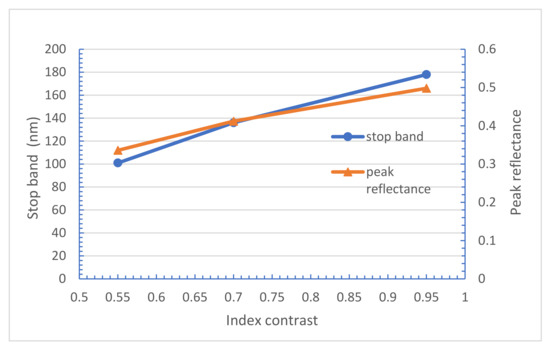
Figure 8.
Plots of stopband width and bottom mirror peak reflectance versus refractive index contrast.
The characteristics of the multimode cavity of the device with emissions at 550 nm based on three periods of DBR are discussed. We have investigated different devices based on the three types of DBR with varying cavity modes through changing the cavity length. The cavity lengths of several resonance modes are given by Equation (3); by varying mode index (m = 1, m = 2 and m = 3), the cavity length can be adjusted for resonance mode. Table 3 summarizes the main characteristic parameters of the device with emission at 550 nm for three cavity modes. Clearly, the highest cavity enhancement factor and photon lifetime is obtained for the device with mode index m = 3 and attributed to the increase in the cavity length at this mode.
Table 3.
Cavity characteristics of the device with three periods of DBR3 at 550 nm.
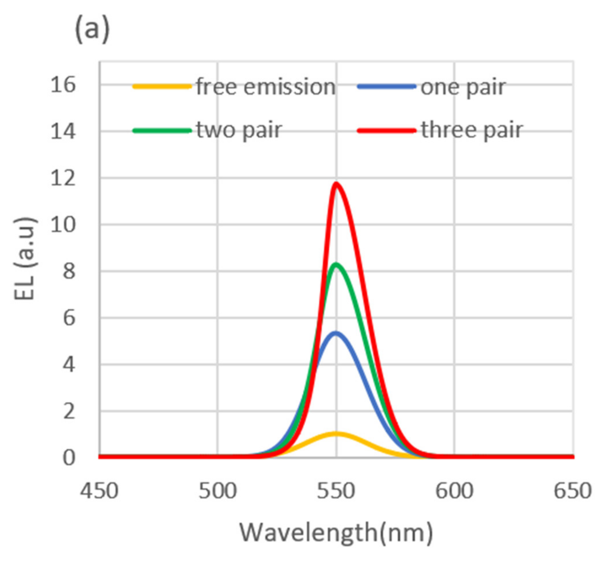
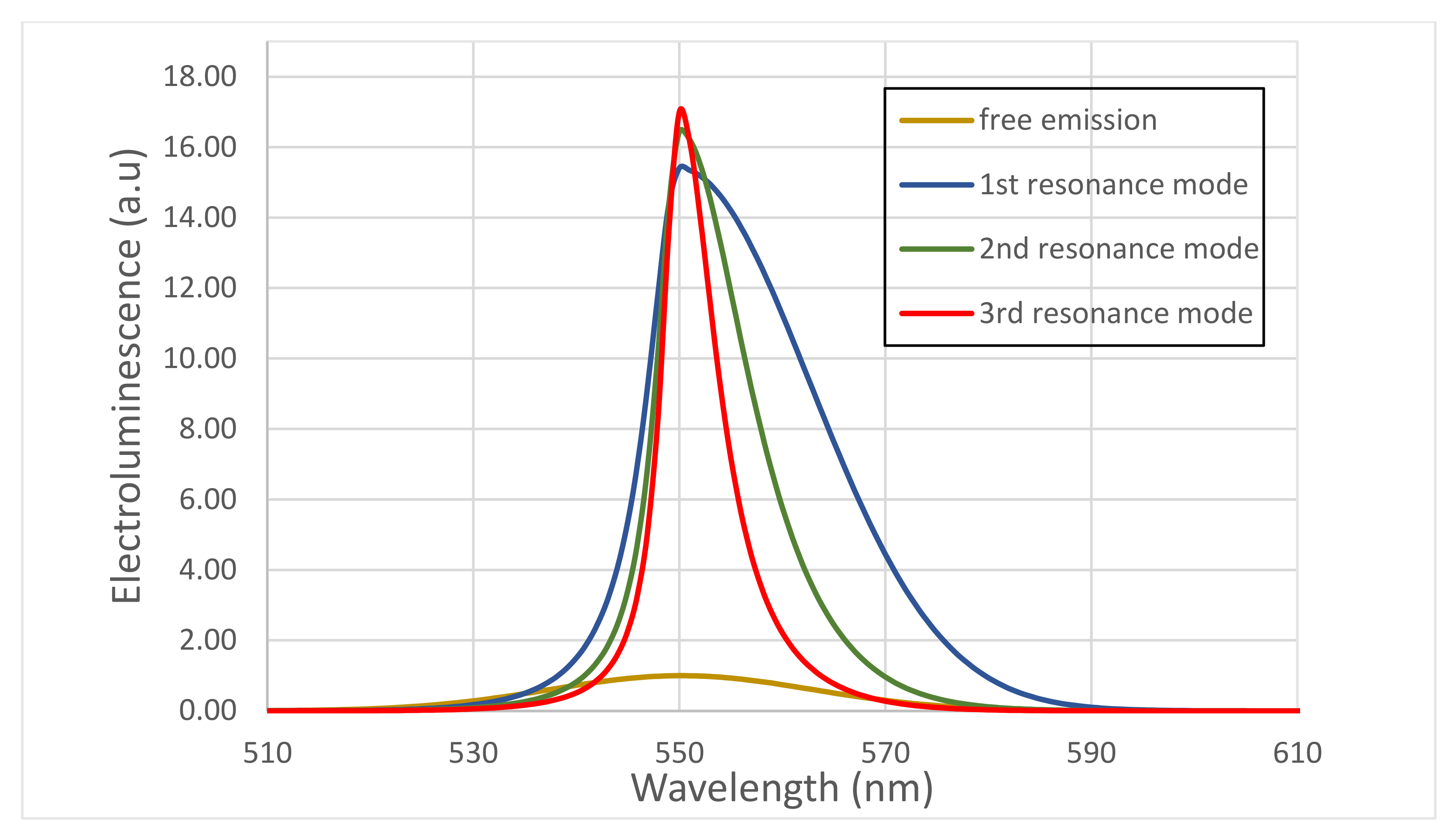
The external emission intensity spectrum of the devices was simulated using Equation (2) with an increasing number of periods of DBR1, DBR2, and DBR3. The obtained intensities of the emission peaks are presented in Table 2. The emission spectra of all devices with different structures of DBR are shown in Figure 9a–c. Clearly, the number of periods causes a pronounced effect on the emission characteristics. The emission spectrum’s full width at half maximum (FWHM) decreases, and the peak intensity increases at the resonance wavelength as the number of periods increases. The improvement in the output light intensity of devices with increasing period number is ascribed to the increase in reflectivity. It is worth mentioning that the performance of the device based on DBR3 consisting of ZnS/CaF2 revealed better performance relative to other devices. Consequently, we selected the device based on DBR3 consisting of ZnS/CaF2 to investigate the effect of resonance mode on the emission spectra. Furthermore, ZnS/CaF2 possesses low absorption and a high index of contrast for emission at 550 nm. In addition, future fabrication of ZnS/CaF2 can be carried out on the substrate at room temperature, which benefits consuming time and avoiding damage to soft materials. The electroluminescence spectra of the device with three cavity modes are shown in Figure 10. Increasing the mode index of the cavity leads to a pronounced improvement in emission intensity. The increase in emission intensity is attributed to the increase in cavity length. Furthermore, the increase in cavity mode leads to the enhancement of the central wavelength at the expense of the other wavelengths and consequently causes a pronounced decrease in the line width.

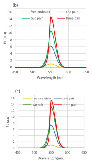
Figure 9.
Electroluminance spectra for devices based on (a) DBR1 (b) DBR2 (c) DBR3.

Figure 10.
Electroluminescence spectra of device based on DBR3 at three-resonance mode.
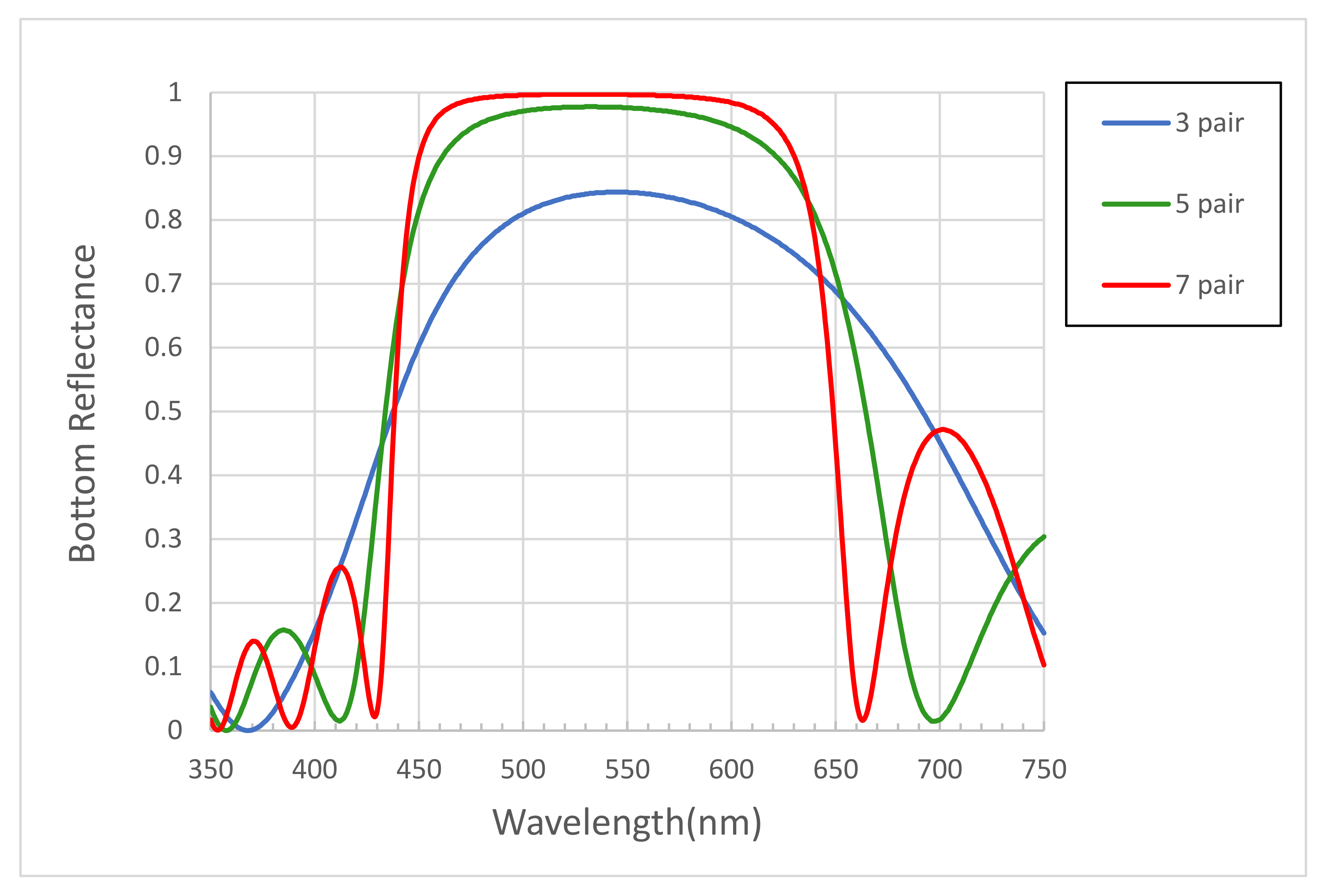
To verify the validity of the methodology (TMM) that we used in this work, we applied this method to calculate the bottom reflectance of the device fabricated by Kitabayashi et al. [20]. In this calculation, we have considered the same values of layer thickness in the published work. Figure 11 shows the calculated bottom reflectance spectra of the device fabricated by Kitabayashi et al. [20] with 3, 5, and 7 pairs of ZnS/CaF2 DBR. The comparison between the calculated bottom reflectance and the measured values at a wavelength of 550 nm of the device fabricated by Kitabayashi et al. [20] is shown in Table 4. The results indicated that the calculated bottom reflectances are compatible with the measured experimental results.

Figure 11.
Calculated bottom reflection spectra of the device fabricated by Kitabayashi et al. [20].
Table 4.
The measured and calculated bottom reflectance at 550 nm of the device fabricated by Kitabayashi et al. [20] with different pairs of ZnS/CaF2 DBR.
4. Conclusions
The external emissions of microcavity light-emitting devices based on Zn (Te, Se) alloy quantum dots as an active layer and organic structures as electron and hole-transporting layers were investigated. The mirrors of the microcavity consist of one mirror with extreme reflection, consisting of a dense dielectric distributed Bragg reflector (DBR), and other metal mirrors with low work functions. The emission characteristics based on the variation in the number of periods of DBR and cavity length were investigated. The increase in the number of periods of DBR or refractive index contrast causes a pronounced increase in reflectivity, which in turn improves the eternal emission of the light-emitting devices. Additionally, the increase in the mode index of the cavity with adjusting cavity length leads to a pronounced improvement in emission intensity.
Author Contributions
Conceptualization, I.E.S., A.S.S. and S.W.; methodology, I.E.S. and S.W.; software, I.E.S. and A.S.S.; formal analysis, I.E.S., A.S.S., S.M. and S.W.; investigation, I.E.S., A.S.S., S.M. and S.W.; data curation, I.E.S., A.S.S., S.M. and S.W.; writing—original draft preparation, I.E.S.; writing—review and editing, I.E.S., A.S.S., S.M. and S.W.; supervision, A.S.S. and S.W.; project administration, S.M.; funding acquisition, S.M. All authors have read and agreed to the published version of the manuscript.
Funding
The authors acknowledge the support and funding of Research Center for Advanced Material Science (RCAMS) at King Khalid University through Grant No. RCAMS/KKU/009-21. Authors acknowledge the support provided by King Abdullah City for Atomic and Renewable Energy (K.A.CARE) under K.A.CARE-King Abdulaziz University Collaboration Program.
Informed Consent Statement
Not applicable.
Data Availability Statement
All data generated or analyzed during this study are included in this article.
Conflicts of Interest
The authors declare no conflict of interest.
References
- Melville, J.; Kapelewski, M. Optical Properties of Quantum Dots; UC Berkeley College of Chemistry: Berkeley, CA, USA, 2015; pp. 2–3. [Google Scholar]
- Ibrahim, A.; El-Sayed, N.; Kaid, M.; Ashour, A. Structural and electrical properties of evaporated ZnTe thin films. Vacuum 2004, 75, 189–194. [Google Scholar] [CrossRef]
- Tsukuda, S.; Kita, M.; Omata, T. Zn (Te1 − xSex) quantum dots synthesized through a facile route and their band-edge and surface state driven visible-light emission. J. Lumin. 2021, 231, 117829. [Google Scholar] [CrossRef]
- Wageh, S. Ternary ZnS: Te nanoparticles capped with 3-mercaptopropionic acid prepared in aqueous media. J. Mater. Sci. Mater. Electron. 2016, 27, 10877–10887. [Google Scholar] [CrossRef]
- Chang, L.; Cheng, J.; Hsu, C.; Chao, H.; Li, W.; Chang, Y.; Chen, K.; Chen, Y.; Laing, C.-T. Isoelectronic centers and type-II quantum dots: Mechanisms for the green band emission in ZnSeTe alloy. J. Appl. Phys. 2009, 105, 113511. [Google Scholar] [CrossRef]
- Asano, H.; Arai, K.; Kita, M.; Omata, T. Synthesis of colloidal Zn (Te, Se) alloy quantum dots. Mater. Res. Express. 2017, 4, 106501. [Google Scholar] [CrossRef] [Green Version]
- Asano, H.; Tsukuda, S.; Kita, M.; Fujimoto, S.; Omata, T. Colloidal Zn (Te, Se)/ZnS core/shell quantum dots exhibiting narrow-band and green photoluminescence. ACS Omega 2018, 3, 6703–6709. [Google Scholar] [CrossRef] [PubMed] [Green Version]
- Asano, H.; Omata, T. Design of cadmium-free colloidal II–VI semiconductor quantum dots exhibiting RGB emission. AIP Adv. 2017, 7, 045309. [Google Scholar] [CrossRef] [Green Version]
- Patra, S.K.; Bhushan, B.; Priyam, A. Water-soluble, luminescent ZnTe quantum dots: Supersaturation-controlled synthesis and self-assembly into nanoballs, nanonecklaces and nanowires. Dalton Trans. 2016, 45, 3918–3926. [Google Scholar] [CrossRef] [PubMed]
- Adachi, S. Optical Constants of Crystalline and Amorphous Semiconductors. In Numerical Data and Graphical Information; Kluwer Academic Publishers: Boston, MA, USA, 1999. [Google Scholar]
- Zhang, H.; Su, Q.; Chen, S. Quantum-dot and organic hybrid tandem light-emitting diodes with multi-functionality of full-color-tunability and white-light-emission. Nat. Commun. 2020, 11, 1–8. [Google Scholar] [CrossRef] [PubMed]
- Wageh, S. Light emitting devices based on CdSe nanoparticles capped with mercaptoacetic acid. IEEE J. Quantum Electron. 2014, 50, 1–8. [Google Scholar] [CrossRef]
- Prontera, C.T.; Pugliese, M.; Giannuzzi, R.; Carallo, S.; Esposito, M.; Gigli, G.; Maiorano, V. Flexible distributed Bragg reflectors as optical outcouplers for OLEDs based on a polymeric anode. J. Inf. Disp. 2021, 22, 39–47. [Google Scholar] [CrossRef]
- Assafli, H.T.; Abdulhadi, A.H.; Nassir, W.Y. Design High Efficient Reflectivity of Distributed Bragg Reflectors. Iraqi J. Laser 2016, 15, 15–20. [Google Scholar]
- Dong, W.J.; Lo, N.-T.; Jung, G.H.; Ham, J.; Lee, J.-L. Efficiency enhancement and angle-dependent color change in see-through organic photovoltaics using distributed Bragg reflectors. Appl. Phys. Lett. 2016, 108, 103902. [Google Scholar] [CrossRef]
- Delbeke, D.; Bockstaele, R.; Bienstman, P.; Baets, R.; Benisty, H. High-efficiency semiconductor resonant-cavity light-emitting diodes: A review. IEEE J. Sel. Top. Quantum Electron. 2002, 8, 189–206. [Google Scholar] [CrossRef]
- Wu, Y.; Yang, J.; Wang, S.; Ling, Z.; Zhang, H.; Wei, B. High-performance white organic light-emitting diodes using distributed Bragg reflector by atomic layer deposition. Appl. Sci. 2019, 9, 1415. [Google Scholar] [CrossRef] [Green Version]
- Tan, X.; Tu, Y.; Deng, C.; von Czarnowski, A.; Yan, W.; Ye, M.; Yi, Y. Enhancement of light trapping for ultrathin crystalline silicon solar cells. Opt. Commun. 2018, 426, 584–588. [Google Scholar] [CrossRef]
- Lohithakshan, L.C.; Geetha, V.; Kannan, P. Single polymer-variable index for the design and fabrication of variable stop band distributed Bragg reflectors. Opt. Mater. 2020, 110, 110509. [Google Scholar] [CrossRef]
- Kitabayashi, T.; Asashita, T.; Satoh, N.; Kiba, T.; Kawamura, M.; Abe, Y.; Kim, K.H. Fabrication and characterization of microcavity organic light-emitting diode with CaF2/ZnS distributed Bragg reflector. Thin Solid Films 2020, 699, 137912. [Google Scholar] [CrossRef]
- Zhang, J.; Zhang, H.; Zheng, Y.; Wei, M.; Ding, H.; Wei, B.; Zhang, Z. Super color purity green organic light-emitting diodes with ZrO2/zircone nanolaminates as a distributed Bragg reflector deposited by atomic layer deposition. Nanotechnology 2016, 28, 044002. [Google Scholar] [CrossRef]
- Martin, L.F.; Patwardhan, A.M.; Jain, S.V.; Salloum, M.M.; Freeman, J.; Khanna, R.; Gannala, P.; Goel, V.; Jones-MacFarland, F.N.; Killgore, W.D. Evaluation of green light exposure on headache frequency and quality of life in migraine patients: A preliminary one-way cross-over clinical trial. Cephalalgia 2021, 41, 135–147. [Google Scholar] [CrossRef] [PubMed]
- Manaf, N.A.A.; Alias, M.S.; Mithani, S.M.; Maulud, M.F.; Yahya, M.R.; Mat, A.F.A. Design and optimization of distributed Bragg reflector for 1310nm vertical cavity surface emitting lasers. In Proceedings of the 2008 IEEE International Conference on Semiconductor Electronics ICSE, Johor Bahru, Malaysia, 25–27 November 2008; pp. 254–258. [Google Scholar]
- Zhang, C.; ElAfandy, R.; Han, J. Distributed Bragg reflectors for GaN-based vertical-cavity surface-emitting lasers. Appl. Sci. 2019, 9, 1593. [Google Scholar] [CrossRef] [Green Version]
- Sharhan, A.A. Transfer Matrix Mathematical Method for Evaluation the DBR Mirror for Light Emitting Diode and Laser. J. Phys. Conf. Ser. 2020, 1535, 1–7. [Google Scholar] [CrossRef]
- Poitras, D.; Kuo, C.-C.; Py, C. Design of high-contrast OLEDs with microcavity effect. Opt. Express 2008, 16, 8003–8015. [Google Scholar] [CrossRef] [PubMed]
- Chen, S.; Deng, L.; Xie, J.; Peng, L.; Xie, L.; Fan, Q.; Huang, W. Recent developments in top-emitting organic light-emitting diodes. Adv. Mater. 2010, 22, 5227–5239. [Google Scholar] [CrossRef]
- Varu, H. The Optical Modelling and Design of Fabry Perot Interferometer Sensors for Ultrasound Detection. Ph.D. Thesis, University College London, London, UK, 2014. [Google Scholar]
- Tadayon, M.A.; Baylor, M.-E.; Ashkenazi, S. High quality factor polymeric Fabry-Perot resonators utilizing a polymer waveguide. Opt. Express 2014, 22, 5904–5912. [Google Scholar] [CrossRef] [PubMed]
- Thomschke, M.; Nitsche, R.; Furno, M.; Leo, K. Optimized efficiency and angular emission characteristics of white top-emitting organic electroluminescent diodes. Appl. Phys. Lett. 2009, 94, 59. [Google Scholar] [CrossRef]
- Hadjaj, F.; Belghachi, A.; Halmaoui, A.; Belhadj, M.; Mazouz, H. Study of a Fabry-Perot resonator. Int. J. Phys. Math. Sci. 2013, 7, 1713–1717. [Google Scholar]
- Darrow, M.C. Finesse Measurement in Fabry-Perot Interferometers. Macalester J. Phys. Astron. 2014, 2, 3. [Google Scholar]
- Gryshchenko, S.; Demin, A.; Lysak, V. Quantum efficiency and reflection in resonant cavity photodetector with anomalous dispersion mirror. In Proceedings of the 2008 4th International Conference on Advanced Optoelectronics and Lasers IEEE, Alushta, Ukraine, 29 September–4 October 2008; pp. 229–232. [Google Scholar]
- Coldren, L.A.; Corzine, S.W. Diode Lasers and Photonic Integrated Circuits; John Wiley & Sons Inc: New York, NY, USA, 1995. [Google Scholar]
- Yahia, K.Z. Simulation of multilayer layer antireflection coating for visible and near IR region on silicon substrate using MATLAB program. Al-Nahrain J. Sci. 2009, 12, 97–103. [Google Scholar]
- Born, M.; Wolf, E. Principles of Optics: Electromagnetic Theory of Propagation, Interference and Diffraction of Light; Elsevier: Amsterdam, The Netherlands, 2013. [Google Scholar]
- Shaaban, I.E.; Samra, A.S.; Yousif, B.; Alghamdi, N.; El-Sherbiny, S.; Wageh, S. Cavity Design and Optimization of Hybrid Quantum Dot Organic Light Emitting Devices for Blue Light Emission. J. Nanoelectron. Optoelectron. 2020, 15, 1364–1373. [Google Scholar] [CrossRef]
- Wang, L.-W.; Zunger, A. Pseudopotential calculations of nanoscale CdSe quantum dots. Phys. Rev. B 1996, 53, 9579. [Google Scholar] [CrossRef] [Green Version]
- Li, H. Refractive index of ZnS, ZnSe, and ZnTe and its wavelength and temperature derivatives. J. Phys. Chem. Ref. Data 1984, 13, 103–150. [Google Scholar] [CrossRef]
- Wood, D.L.; Nassau, K. Refractive index of cubic zirconia stabilized with yttria. Appl. Opt. 1982, 21, 2978–2981. [Google Scholar] [CrossRef] [PubMed]
- Rodríguez-de Marcos, L.V.; Larruquert, J.I.; Méndez, J.A.; Aznárez, J.A. Self-consistent optical constants of SiO2 and Ta2O5 films. Opt. Mater. Express 2016, 6, 3622–3637. [Google Scholar] [CrossRef]
- Duttagupta, S.; Ma, F.; Hoex, B.; Mueller, T.; Aberle, A.G. Optimised antireflection coatings using silicon nitride on textured silicon surfaces based on measurements and multidimensional modelling. Energy Procedia 2012, 15, 78–83. [Google Scholar] [CrossRef] [Green Version]
- Cheng, F.; Su, P.-H.; Choi, J.; Gwo, S.; Li, X.; Shih, C.-K. Epitaxial growth of atomically smooth aluminum on silicon and its intrinsic optical properties. ACS Nano 2016, 10, 9852–9860. [Google Scholar] [CrossRef] [PubMed]
- Moerland, R.J.; Hoogenboom, J.P. Subnanometer-accuracy optical distance ruler based on fluorescence quenching by transparent conductors. Optica 2016, 3, 112–117. [Google Scholar] [CrossRef]


Publisher’s Note: MDPI stays neutral with regard to jurisdictional claims in published maps and institutional affiliations. |
© 2022 by the authors. Licensee MDPI, Basel, Switzerland. This article is an open access article distributed under the terms and conditions of the Creative Commons Attribution (CC BY) license (https://creativecommons.org/licenses/by/4.0/).