Article

ZVS Realization of H-Bridge Low-Voltage High-Current Converter via Phase-Shift and Saturable Control

1
School of Electrical and Mechanical Engineering, Zhongshan Polytechnic, Zhongshan 528404, China
2
School of Mechanical & Automotive Engineering, South China University of Technology, Guangzhou 510641, China
3
School of Engineering, Deakin University, Melbourne 3125, Australia
4
Zhongshan Baolijin Electronics Co., Ltd., Zhongshan 528451, China
*
Author to whom correspondence should be addressed.
Energies 2022, 15(24), 9488; https://doi.org/10.3390/en15249488
Submission received: 14 November 2022 / Revised: 9 December 2022 / Accepted: 12 December 2022 / Published: 14 December 2022

Abstract

:
A zero-voltage switching (ZVS) H-bridge phase-shifted low-voltage high-current converter with saturable inductors is proposed in this paper. The introduction of saturable inductors solves the short circuit problem caused by high-frequency on–off of the power tube, and effectively inhibits high-frequency voltage oscillation and voltage spikes of the rectifier tube. In addition, when the current flowing through the saturable inductor does not change rapidly, it exhibits a low impedance and consumes very little power. The detailed design process of main parameters in the converter is presented to provide design reference for power supply workers. To verify the effectiveness of design, a 3 kW(15 V/200 A) prototype converter is built. This low-voltage high-current prototype has around 90% efficiency, and can suppress high-frequency voltage oscillation and voltage spikes, avoiding the short circuit problem of power tube, all of which are verified by experimentation.

1. Introduction

The full-bridge (also named as H-bridge) zero-voltage switching PWM (FB-ZVS PWM) converter [1,2,3,4,5,6,7] uses the leakage inductance of the transformer and the parasitic capacitance of the power tube to achieve zero-voltage switching [8,9,10], which greatly reduces the switching loss and has been widely used in high power DC–DC converters [11,12,13,14,15,16,17,18]. However, in the bridge converter, high-frequency on–off of the power tube causes serious interference signals, which can cause short circuit problems of power tubes in the same bridge arm [19]. When the rectifier tube is in the reverse recovery state, it will generate high-frequency voltage oscillations and voltage spikes, which exacerbate voltage stresses as well as reverse recovery power loss, and cause serious EMI problems [14,20,21,22].
In order to solve the short circuit problem caused by the high-frequency voltage oscillation and voltage spikes, many methods have been proposed. For example, some have adopted the RC absorption circuit in the converter [23]. When the switch is turned off, the energy accumulated in the parasitic inductor charges the absorption capacitor to suppress the voltage surge. However, parameter design of RC absorption circuit is difficult, and inappropriate parameter design will increase the power loss of the circuit, and it cannot achieve the expected ripple suppression. Some have used the RCD absorption circuit in the converter [9,23]. When the switching voltage rises to the voltage of the absorption capacitor, the absorption diode is turned on, so the switch is embedded by the diode. However, the diode of the RCD absorption circuit has large power loss and RCD absorption circuit is not suitable for the absorption of diode reverse voltage spike, because it may exacerbate the diode reverse recovery current. Some have employed the Zener clamp circuit [24,25], which adds the Zener diode at the primary or secondary side. The voltage of the Zener diode aggravates the clamped below the maximum voltage when the current rises. However, the rapid conduction of Zener diode will exacerbate EMI problem. Some researchers proposed the chaotic spread spectrum technique [20,26]. It utilizes the wide spectrum characteristics of chaotic signals to distribute the energy to a wider continuous frequency band, so as to achieve EMI suppression. Some scholars put forward that the understanding of the DCM resonance mechanism is the key to fulfilling ZVS and ZCS simultaneously [27]. Some researchers proposed the new modulation strategy without introducing an auxiliary circuit [28]. However, these methods generally are complex and lack of practicability. Some researchers introduce an auxiliary current source network to realize the zero-voltage turn-on of the lagging bridge arm, but it is complex [29]. Some proposed FFM modulation-based soft-switched isolated SRC to reduce the conduction losses by blocking the reverse current [30]. Figure 1 shows the methods used in resolving voltage oscillation and voltage spike problems.
In this paper, a ZVS H-bridge phase-shifted low-voltage high-current converter with saturable inductors (ZVS-HBPS-LVHC-SI) is proposed. Its overall topology is similar to FB-ZVS PWM, but compared with FB-ZVS PWM, the proposed method adds saturable inductors before the rectifier diode at the secondary side and saturable inductors to the drive circuit. In this way, circuit performance can be improved without changing the circuit structure. Saturable inductors are used to inhibit the turn-off voltage spike of the power tubes as well as diodes, and reduce the influence of resonance on the driving waveform, which resolve the short circuit problem of the bridge arm. Finally, a detailed saturable inductor design is provided and a 3 KW (15 V/200 A) ZVS H-bridge phase-shifted low-voltage high-current converter is built to verify the effectiveness of the design.

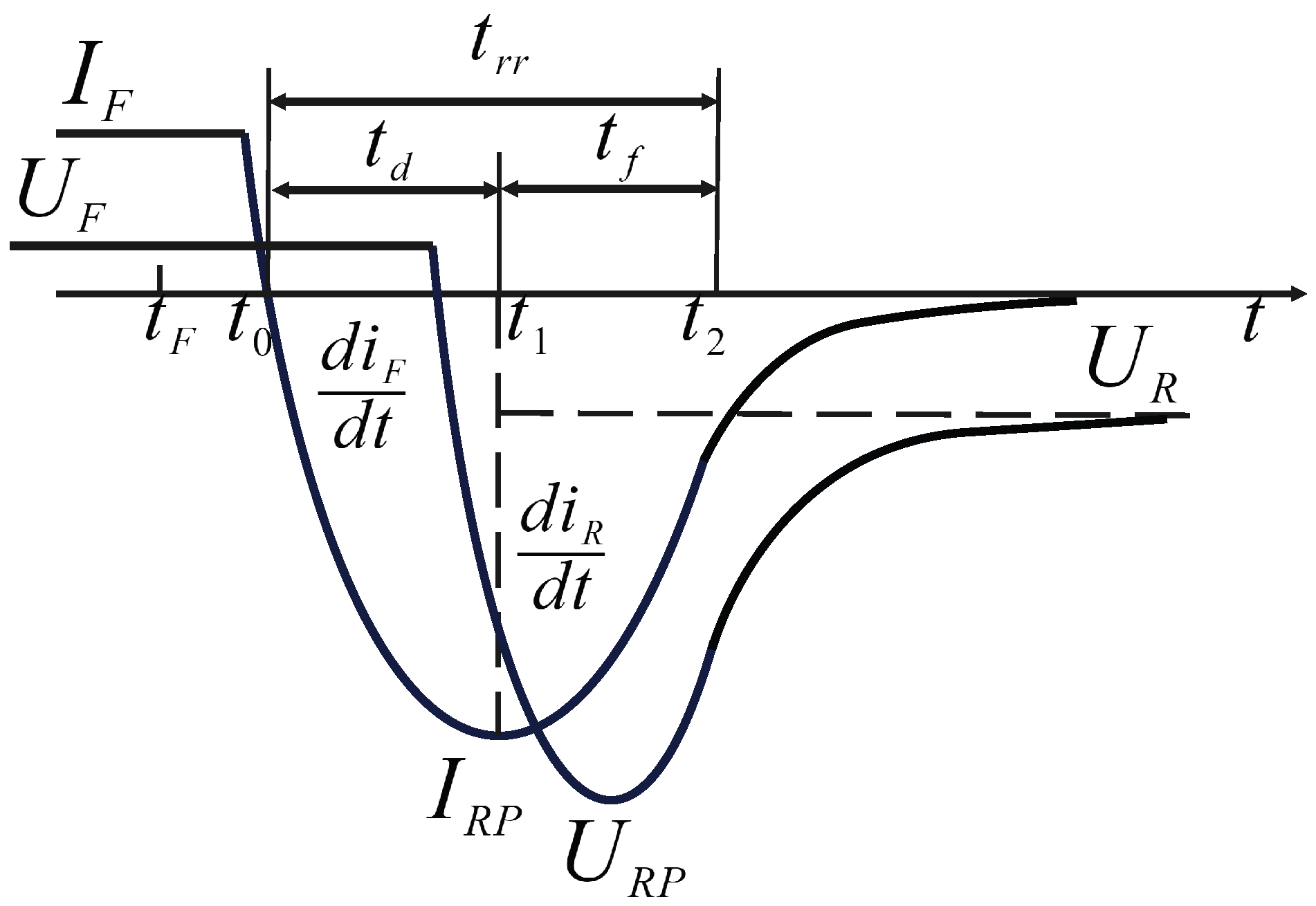
2. Voltage Spikes Generation and Suppression

2.1. Voltage Spike Generation Mechanism

Due to the existence of junction capacitance, the rectifier tube must experience a transient process when it switches state among zero bias, forward bias and reverse bias. It takes the rectifier tube a certain amount of time to restore the reverse blocking ability when the reverse voltage is suddenly applied to it. The dynamic reverse recovery characteristics of the rectifier tube are shown in Figure 2, where I F is the forward conduction current, and t rr is the reverse recovery time of the rectifier tube.
After t 1 , the rapid decline in reverse current results in a high value of d i R d t . Then, due to the influence of inductance, reverse voltage spike U RP is generated. The spike may reach more than three times the voltage at the secondary side.

2.2. Voltage Spike Suppression with Saturable Inductors

In order to better understand the mechanism of voltage spike suppression with saturable inductors, secondary circuit of ZVS-HBPS-LVHC-SI is used to illustrate. Figure 3 shows the secondary circuit of ZVS-HBPS-LVHC-SI, where both L s 1 and L s 2 are saturable inductors and reach their saturation regions when the reverse current rises. Figure 4 shows working modes of the secondary circuit. When rectifier tube D S 1 and D S 1 convert from one state to another, they will experience reverse recovery state and then generate high-frequency voltage oscillation and voltage spikes, which lead to voltage stress increase, reverse recovery power loss, and serious EMI problems.
To resolve this problem, saturable inductors are introduced as shown in Figure 3. Saturable inductors are the inductors with high rectangular hysteresis loop, high initial permeability and obvious magnetic saturation point. When the current is small, saturable inductor is equivalent to open circuit and the inductor is not saturated. When the current is large, saturable inductor is equivalent to a short circuit and the inductor is saturated. When the external voltage is applied, the initial current inside the inductor increases slowly at first. Only when the current in the inductor reaches a certain value do inductors L s 1 and L s 2 become saturated immediately.
Figure 5 is the reverse recovery current waveform of the rectifier tube after adding saturable inductors. When current rises rapidly, the inductors become saturated immediately and have high impedance, so the upward trend of reverse current becomes flat and the peak current I RP as well as peak voltage U RP are reduced. In addition, the reverse recovery time of the rectifier tube after adding saturable inductors is approximately π t rr .
Saturable inductors can inhibit current growth and thus can suppress voltage spike effectively. In addition, saturable inductors have low power loss because they only have high impedance when current changes rapidly, and the impedance is kept low.

3. Parameters Design in the Converter

3.1. Design of the Circuit

The main circuit of ZVS-HBPS-LVHC-SI is shown in Figure 6. Q 1 and Q 3 are the leading-bridge power tubes. Q 2 and Q 4 are the lagging-bridge power tubes. These four power tubes make up the H-bridge inverter circuit. C b is the DC-blocking capacitor. L r is the leakage inductance of transformer T. D 5 and D 6 are the clamping diodes of the leading-bridge circuit. D c , R c and C c constitute up the RCD circuits of the lagging-bridge arm. L s 1 and L s 2 are saturable inductors at the secondary side. D s 1 and D s 2 are rectifier diodes at the secondary side. D s 3 is the freewheeling diode at the secondary side. In Figure 6, inductors in the dotted box are saturable inductors. Compared with the traditional ZVS circuit, ZVS-HBPS-LVHC-SI has a similar structure but adds saturable inductors L s 1 and L s 2 to inhibit high-frequency voltage oscillation and voltage spikes. When current rises, the saturable inductors will have high impedance, which slows the rising of current and consequently suppresses voltage.

3.2. Design of Drive Circuit

In order to avoid misleading power tubes in the same bridge arm caused by interference signal, this paper designs a drive circuit that can effectively suppress the voltage amplitude of the interference signal, as shown in Figure 7.
In Figure 7, capacitors C 4 and C 5 are equivalent to voltage sources to achieve rapid turn-off together with the transistor Q 5 and Q 6 . L 1 and L 2 are saturable inductors. The drive circuit outputs the PWM signal to Q 1 , Q 2 , Q 3 , Q 4 when receiving the control signal. Compared with the drive circuit of traditional FB-ZVS PWM, saturable inductors L 1 and L 2 are used before the output drive signal to reduce high-frequency interference signal peak, which causes the short-circuit problem of the power tubes. Its mechanism is the same as diode peak suppression. Both of them make use of the characteristics of the saturable inductor to inhibit current growth.

3.3. Detailed Design of High-Frequency Transformer

The minimum input value of the three-phase AC voltage U acmin is calculated as follows,
U acmin = 380 1 10 % = 342 V
Therefore, the DC bus voltage is about 483V. Calculated with the bus voltage change rate of 10 % , the minimum bus output voltage U dcmin is expressed as follows,
U dcmin = 483 1 10 % = 435 V
Ignoring the voltage drop of diodes and setting the largest voltage drop on the DC blocking capacitor as 5 % of the bus voltage, the input voltage in the primary side is calculated as
U Tpri = U dcmin 1 5 %
Insert ( 2 ) into ( 3 ) ,
U Tpri = 435 × 1 5 % = 413 V
To calculate the output voltage U Tsec required for the secondary side of the transformer, the duty cycle loss, the voltage drop of the rectifier diode at the secondary side and the voltage drop of the output filtering inductor should be considered. The ideal output voltage of the power supply U o is 15 V. The maximum effective duty ratio D max is 0.85. The tube voltage drop U r is 0.7 V and U L is 0.3 V. Output voltage U Tsec is calculated as
U Tsec = U o + U r + U L D max = 15 + 0.7 + 0.3 0.85 = 18.8 V
From ( 4 ) and ( 5 ) , the transformer ratio K is calculated as follows,
K = U Tpri U Tsec = 413 18.8 = 22
The switching period T is 10 μ s calculated with 100 kHz switching frequency, and the maximum duty ratio Δ max is 45 % . Considering the shielding electromagnetic interference and volume of the transformer, PQ40 magnetic core is selected in this paper. According to the TDK magnetic core parameter manual, the effective magnetic flux area A e is 201 mm 2 and the maximum magnetic flux density B is 3000 Gs. Therefore, the number of turns of the transformer at the primary side is calculated as
N pri = U dcmin T Δ max 2 B A e = 413 × 10 × 0.45 × 10 6 2 × 3000 × 201 × 10 10 = 16
Since the transformer ratio k is 22 and the number of turns of the secondary side transformer is minimum 1 turn, the number of turns of the primary side transformer is at least 22 turns. Therefore, the transformer magnetic core can reserve 30% magnetic flux. The decrease of magnetic flux density can greatly reduce the iron loss of the magnetic core and temperature rise of the working transformer.

3.4. Detailed Design of Saturable Inductors

Saturable inductors have large inductance when the rectifier tube is in the reverse recovery state. To eliminate the impact of minority carrier’s reverse recovery, its volt-second characteristics must meet the following,
2 V s t s = N Δ B A e
In ( 8 ) , V s is the voltage of the transformer’s secondary side. t s is the recombination time of minority carrier in rectifier tubes’ reverse recovery state. n is the number of turns of the depressor. B is the range of magnetic density. A e is the effective magnetic core area.
According to ( 8 ) , the number of turns of the saturable inductors N is calculated as follows:
N = 2 V s t s Δ B A e
After adding the saturable inductors, the reverse recovery time of the rectifier tube is about π t rr , where t rr is the reverse recovery time of the rectifier tube without saturable inductors. The number of turns of the saturable inductors N must satisfy
N = 2 V s I F π t rr Δ B A e F cu J W
The VITROVAC 6025Z, a cobalt-based amorphous magnetic core, is selected as the magnetic core of the saturable inductor. It has the characteristics of high permeability, low core loss and high rectangular ratio B s / B r . Its saturation magnetic induction intensity B s is 0.8∼1.2 T, and its coercivity H C is less than 1 A/m. Small coercivity, small area of hysteresis loop and low core iron loss make it suitable for converters with large output currents.

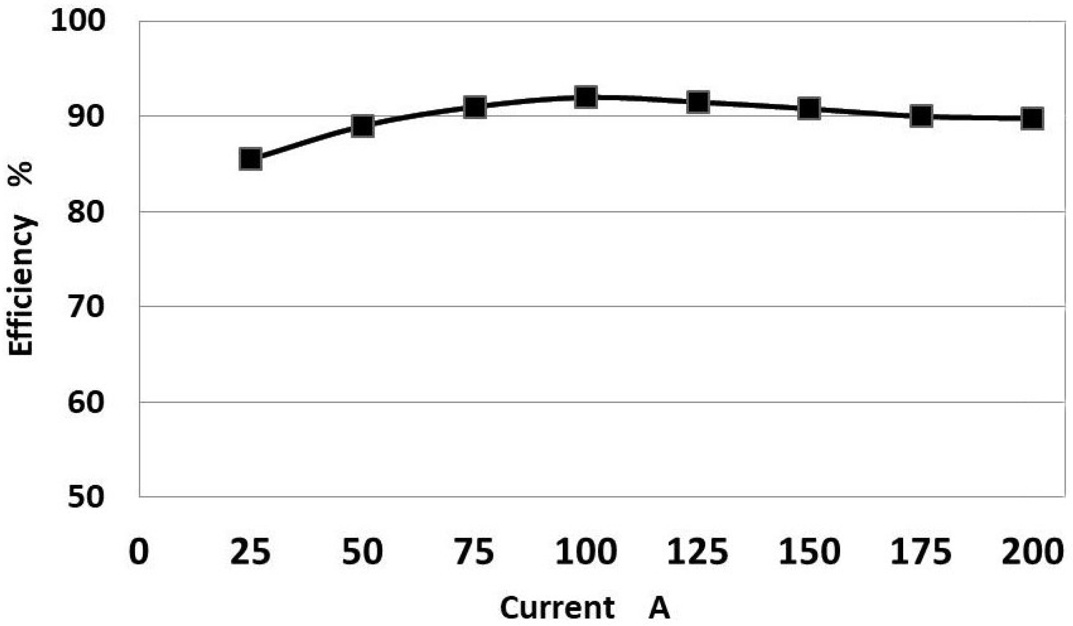
4. Efficiency Analysis

As a result of the introduction of saturable inductors and realization of zero voltage switch, reverse conduction losses of diodes P D R and switching on-off losses of power tubes P Q S are reduced greatly compared with FB-ZVS PWM without saturable inductors. Therefore, the power loss P l o s s of the ZVS-HBPS-LVHC-SI mainly comes from the power tube conduction loss P Q C , control loss of power tubes P Q G , diode conduction loss P D C and transformer loss P T . These are the power losses that inevitably occur when components work. The power loss P l o s s can be calculated as follows:
P l o s s = P Q C + P Q G + P D C + P T
V o u t is the output voltage of the ZVS-HBPS-LVHC-SI, and the output power P o u t of the ZVS-HBPS-LVHC-SI can be calculated as follows:
P o u t = V o u t 2 R L
Table 1 is the main power loss of the ZVS-HBPS-LVHC-SI [31].
The efficiency η of the ZVS-HBPS-LVHC-SI can be calculated as follows:
η = P o u t P l o s s + P o u t × 100 %

5. Experimental Verification

In order to verify the performance of the improved circuit, a 3 kW(15 V/200 A) ZVS-HBPS-LVHC-SI is designed. The prototype parameters are shown in Table 2. In addition, an application field of the ZVS-HBPS-LVHC-SI is electroplating power supply, which is always high-power-consuming and with low efficiency. The power design and component parameter design of the prototype are carried out according to the electroplating power supply standard, which can prove that the introduction of saturable inductance reduces the power consumption and improves the efficiency.
The prototype and experimental environment are shown in Figure 8.
Figure 9 presents the efficiency curve of the converter. As the power increases, at half load, the efficiency of the power supply reaches 91 % . When the current is 200 A, due to the increase of conduction loss, the efficiency of circuit declines, but it is still approximately 90 % .
Figure 10a shows the driving voltage waveform without saturable inductors. Figure 10b shows the driving voltage waveform with saturable inductors. Figure 11a shows the voltage waveform of the rectifier tube without adding saturable inductors when V in = 200 VAC. Figure 11b shows the voltage waveform of the rectifier tube after adding saturable inductors. In Figure 10a, the high-frequency on–off switch brings serious EMI problems to the drive signal. In Figure 11a, the peak value is more than twice the normal value. After adding saturable inductors, as shown in Figure 10b and Figure 11b, interference and voltage spikes are effectively suppressed.
Figure 12 shows voltage and current waveforms of the switch after adding saturable inductors. Figure 12a shows switch waveforms when circuit is at full load, and Figure 12b shows switch waveforms when circuit is at 75% load.

6. Conclusions

The high-frequency on-off of the power tube causes high-frequency voltage oscillations, voltage spikes and serious EMI problems, which are the main reasons for short circuit problem of the bridge arm and the spike of the secondary rectifier tube.
In this paper, a ZVS H-bridge phase-shifted low-voltage high-current converter with saturable inductors (ZVS-HBPS-LVHC-SI) is designed. It can effectively inhibit the high-frequency oscillations, improves the electromagnetic compatibility of the converter, and resolves the short circuit problem of the bridge arm by inhibiting interference of the main circuit to the drive circuit.
The circuit analysis and the calculation of the main parameters of the power supply are detailed. To verify the feasibility, a 3 KW (15 V/200 A) low-voltage high-current power supply prototype is designed. This low-voltage high-current prototype has high efficiency around 90%. After adding saturable inductors, high-frequency voltage oscillation and voltage spikes are suppressed well and short circuit problem of power tube can be avoided, which are verified well by experimental waveforms. Compared with other methods, the ZVS-HBPS-LVHC-SI only uses saturable inductors to achieve voltage suppression with simple parameter design. In addition, the introduction of saturable inductors helps to improve the efficiency of the circuit because it reduces the power loss of diodes and power tubes. The proposed design can provide practical references for large power switching power supply workers.

Author Contributions

Conceptualization, P.X.; software, P.X.; validation, P.X.; formal analysis, P.X.; writing—original draft preparation, X.L.; writing—review and editing, S.S.Y.; funding acquisition, L.P. All authors have read and agreed to the published version of the manuscript.

Funding

This research was funded by [National Natural Science Foundation of China] grant numbers [62003091], [Guangdong Youth Innovative Talent Project] grant numbers [2017GkQNCX086], [Science and Technology Projects of Zhongshan, Guangdong Province] grant numbers [2017B1121] and [Major Science and Technology Projects of Zhongshan Polytechnic] grant number [2017KQ01].

Data Availability Statement

Not applicable.

Conflicts of Interest

The authors declare no conflict of interest.

References

  1. Zhang, H.; Isobe, T. An Improved Charge-Based Method Extended to Estimating Appropriate Dead Time for Zero-Voltage-Switching Analysis in Dual-Active-Bridge Converter. Energies 2022, 15, 671. [Google Scholar] [CrossRef]
  2. Zha, D.; Wang, Q.; Cheng, M.; Deng, F.; Buja, G. Regulation Performance of Multiple DC Electric Springs Controlled by Distributed Cooperative System. Energies 2019, 12, 3422. [Google Scholar] [CrossRef] [Green Version]
  3. Wang, Q.; Niu, S. A Novel DC-Coil-Free Hybrid-Excited Machine with Consequent-Pole PM Rotor. Energies 2018, 11, 700. [Google Scholar] [CrossRef] [Green Version]
  4. Sun, T.; Liu, H.; Peng, G.; Tang, P.; Zhang, X. Modeling of ZVS PWM FB DC/DC Converter Based on Equivalent Switching Circuit Model. In Proceedings of the Intelligent Control and Automation, Dalian, China, 21–23 June 2006. [Google Scholar]
  5. Khodabakhsh, J.; Moschopoulos, G. A Study of T-Type and ZVS-PWM Full-Bridge Converters for Switch-Mode Power Supplies. IEEE Trans. Power Electron. 2019, 35, 7145–7159. [Google Scholar] [CrossRef]
  6. Adam, A.; Hou, S.; Chen, J. ZVS Operation Range Analysis and Deadband Conditions of A dual H-bridge Bidirectional DC-DC Converter with Phase Shift Control. In Proceedings of the 2019 IEEE International Conference on Environment and Electrical Engineering and 2019 IEEE Industrial and Commercial Power Systems Europe (EEEIC/I&CPS Europe), Genova, Italy, 11–14 June 2019. [Google Scholar]
  7. Wang, Y.; Zhang, Y.; Wang, Y.; Zhu, L.; Guan, Y.; Chen, S.Z.; Zhang, G.; Yang, L. A Dual-Active-Bridge With Half-Bridge Submodules DC Solid-State Transformer for DC Distribution Networks. IEEE J. Emerg. Sel. Top. Power Electron. 2021, 9, 1891–1904. [Google Scholar] [CrossRef]
  8. Zhang, G.; Zeng, J.; Yu, S.S.; Xiao, W.; Zhang, B.; Chen, S.Z.; Zhang, Y. Control Design and Performance Analysis of a Double-Switched LLC Resonant Rectifier for Unity Power Factor and Soft-Switching. IEEE Access 2020, 8, 44511–44521. [Google Scholar] [CrossRef]
  9. Xue, J.; Xin, Z.; Chen, J.; Wang, H.; Blaabjerg, F. An Improved di/dt -RCD Detection for Short-Circuit Protection of SiC mosfet. IEEE Trans. Power Electron. 2020, 36, 12–17. [Google Scholar] [CrossRef]
  10. Zheng, W.; Hu, C.; Zhao, B.; Su, X.B.; Wang, G.; Hou, X.W.; Gu, B. A Two-Stage DC/DC Isolated High-Voltage Converter with Zero-Voltage Switching and Zero-Current Switching Applied in Electronic Power Conditioners. Energies 2022, 15, 6378. [Google Scholar] [CrossRef]
  11. Kan, R.V.; Agostini, E. Hybrid T-Type ZVS Pulsewidth Modulation DC-DC Converter. IEEE Trans. Ind. Electron. 2021, 68, 9420–9432. [Google Scholar] [CrossRef]
  12. Mishima, T.; Koji, Y. Zero Voltage Soft-Switching Phase-Shift PWM Controlled Three-Level DC-DC Converter for Railway Auxiliary Electric Power Unit. In Proceedings of the 2019 IEEE Applied Power Electronics Conference and Exposition (APEC), Anaheim, CA, USA, 17–21 March 2019. [Google Scholar]
  13. Saeed, J. A ZVS-ZCS phase shift full bridge DC-DC converter with secondary-side control for battery charging applications. Int. J. Circuit Theory Appl. 2018, 46, 1407–1415. [Google Scholar] [CrossRef]
  14. Zhang, G.; Li, Z.; Zhang, B.; Halang, W.A. Power electronics converters: Past, present and future. Renew. Sustain. Energy Rev. 2018, 81, 2028–2044. [Google Scholar] [CrossRef]
  15. Zhang, G.; Chen, J.; Zhang, B.; Zhang, Y. A critical topology review of power electronic transformers: In view of efficiency. Chin. J. Electr. Eng. 2018, 4, 90–95. [Google Scholar] [CrossRef]
  16. Huang, W.; Zhang, S.; Yan, R.H. Novel Spread Spectrum Communication Theory and the Anti-jamming Applications. In Proceedings of the 2021 6th International Conference on Inventive Computation Technologies (ICICT), Coimbatore, India, 20–22 January 2021. [Google Scholar]
  17. Wang, Y.; Wang, Y.; Chen, S.Z.; Zhang, G.; Zhang, Y. A Simplified Minimum DC-Link Voltage Control Strategy for Shunt Active Power Filters. Energies 2018, 11, 2407. [Google Scholar] [CrossRef] [Green Version]
  18. Zhang, G.; Ou, Z.; Qu, L. A Fractional-Order Element (FOE)-Based Approach to Wireless Power Transmission for Frequency Reduction and Output Power Quality Improvement. Electronics 2019, 8, 1029. [Google Scholar] [CrossRef] [Green Version]
  19. Hong, J.; Deng, X.; Zhang, G.; Huang, Z.; Li, X.; Zhang, Y. Sneak Circuit Identification of An Improved Boost Converter with Soft-Switching Realization. IEEE J. Emerg. Sel. Top. Power Electron. 2018, 7, 2394–2402. [Google Scholar] [CrossRef]
  20. Wei, S.; Wen, W. High-Frequency Oscillation of the Active-Bridge-Transformer-Based DC/DC Converter. Energies 2022, 15, 3311. [Google Scholar] [CrossRef]
  21. Li, R.; Xu, D.; Feng, B.; Mino, K.; Umida, H. Efficiency and EMI Analysis for a ZVS-SVM Controlled Three-Phase Boost PFC Converter. In Proceedings of the APEC 07 - Twenty-Second Annual IEEE Applied Power Electronics Conference and Exposition, Anaheim, CA, USA, 25 February–1 March 2007. [Google Scholar]
  22. Zeng, J.; Zhang, G.; Yu, S.S.; Zhang, B.; Zhang, Y. LLC resonant converter topologies and industrial applications—A review. Chin. J. Electr. Eng. 2020, 6, 73–84. [Google Scholar] [CrossRef]
  23. Hren, A.; Korelic, J.; Milanovic, M. RC-RCD clamp circuit for ringing losses reduction in a flyback converter. IEEE Trans. Circuits Syst. II Express Briefs 2006, 53, 369–373. [Google Scholar] [CrossRef]
  24. Qin, W.; Wu, X.; Zhang, J. Current-Feed Single-Switch Forward Resonant DC Transformer (DCX) With Secondary Diode-Clamping. IEEE Trans. Ind. Electron. 2017, 64, 7790–7799. [Google Scholar] [CrossRef]
  25. Song, H.; Zhang, Y.; Gao, J.; Zhang, Y.; Feng, X. Clamping-diode Circuit for Marine Controlled-source Electromagnetic Transmitters. J. Power Electron. A Publ. Korean Inst. Power Electron. 2018, 18, 395–406. [Google Scholar]
  26. Boriskov, P.; Velichko, A.; Shilovsky, N.; Belyaev, M. Bifurcation and Entropy Analysis of a Chaotic Spike Oscillator Circuit Based on the S-Switch. Entropy 2022, 24, 11693. [Google Scholar] [CrossRef] [PubMed]
  27. Kumar, R.; Wu, C.C.; Liu, C.Y.; Hsiao, Y.L.; Chieng, W.H.; Chang, E.Y. Discontinuous Current Mode Modeling and Zero Current Switching of Flyback Converter. Energies 2021, 14, 5996. [Google Scholar] [CrossRef]
  28. Liu, H.; Wang, Y.; Wheeler, P.; Zhou, X.; Zhu, K. A Voltage Spike Suppression Strategy Based on De-Re-Coupling Idea for the Three-Phase High-Frequency Isolated Matrix-Type Inverter. IEEE Trans. Power Electron. 2022, 37, 9024–9034. [Google Scholar] [CrossRef]
  29. Zhao, Y.; Xiao, Q.; Zhang, Z.; Zhao, X.; Lin, D. Research on ZVS Phase-Shifted Full-Bridge Broadband Inverter Based on Auxiliary Current Source. Energies 2022, 15, 8661. [Google Scholar] [CrossRef]
  30. Khan, D.; Hu, P.; Waseem, M.; Yasir Ali Khan, M.; Tahir, M.; Annuk, A. Practical Evaluation of Loss Reduction in Isolated Series Resonant Converter with Fixed Frequency Modulation. Energies 2022, 15, 5802. [Google Scholar] [CrossRef]
  31. Mahafzah, K.A.; Obeidat, M.A.; Al-Shetwi, A.Q.; Ustun, T.S. A Novel Synchronized Multiple Output DC-DC Converter Based on Hybrid Flyback-Cuk Topologies. Batteries 2022, 8, 93. [Google Scholar] [CrossRef]
Figure 1. The methods used in resolving voltage oscillation and voltage spikes problems.
Energies 15 09488 g001
Figure 2. Reverse recovery voltage and current waveform of the rectifier tube.
Energies 15 09488 g002
Figure 3. The secondary circuit of ZVS-HBPS-LVHC-SI.
Energies 15 09488 g003
Figure 4. Working modes of the secondary circuit. (a) Stage I; (b) Stage II.
Energies 15 09488 g004
Figure 5. Reverse recovery current waveform of rectifier tube with saturable inductors.
Energies 15 09488 g005
Figure 6. Main circuit structure of ZVS-HBPS-LVHC-SI.
Energies 15 09488 g006
Figure 7. Structure of the drive circuit.
Energies 15 09488 g007
Figure 8. The prototype and experimental environment.
Energies 15 09488 g008
Figure 9. Efficiency curve.
Energies 15 09488 g009
Figure 10. Voltage waveforms of the drive signal. (a) Without saturable inductors; (b) With saturable inductors.
Energies 15 09488 g010
Figure 11. Voltage waveforms of the rectifier tube. (a) Without saturable inductors; (b) With saturable inductors.
Energies 15 09488 g011
Figure 12. Voltage and current waveforms of the switch after adding saturable inductors. (a) Waveforms at full load; (b) Waveforms at 75% load.
Energies 15 09488 g012
Table 1. The power loss of the ZVS-HBPS-LVHC-SI.
Losses TypeEquationConditions
P Q C i = 1 4 I Q i r m s 2 R Q i I Q i r m s : the average current through Q i
R Q i : the DC resistance of Q i
P Q G 4 Q g V g f Q g : switch gate charge D i or D s
V g : voltage needed to charge the gate
f: switching frequency
P D C i = 1 6 I D i r m s 2 R D i + 5 I D S r m s 2 R D s I D i r m s or I D s r m s : the average current through D i or D s
R D i or R D s :the DC resistance of D i or D s
P T π 4 K f α B β + I T r m s 2 R T α , β , K : Constants related to magnetic materials
I T r m s : the average current through the transformer
R T : the DC resistance of the transformer
Table 2. The prototype parameters.
DeviceParameter
Three-phase AC input voltage U in 380 ( ± 10 % ) U ac
Control chipUCC2895
Power cubeSPP17N80C3 (800 V, 17 A, 0.29 ω )
Output rectifier tubeMBRP400100CT
Main transformer ferrite corePQ40/40Z (TDK)
Publisher’s Note: MDPI stays neutral with regard to jurisdictional claims in published maps and institutional affiliations.

